WO2015102107A1 - Substrat de câblage empilé et dispositif d'inspection comprenant ce dernier - Google Patents
Substrat de câblage empilé et dispositif d'inspection comprenant ce dernier Download PDFInfo
- Publication number
- WO2015102107A1 WO2015102107A1 PCT/JP2015/050011 JP2015050011W WO2015102107A1 WO 2015102107 A1 WO2015102107 A1 WO 2015102107A1 JP 2015050011 W JP2015050011 W JP 2015050011W WO 2015102107 A1 WO2015102107 A1 WO 2015102107A1
- Authority
- WO
- WIPO (PCT)
- Prior art keywords
- via conductor
- wiring board
- ceramic
- laminate
- dummy
- Prior art date
Links
Images


Classifications
-
- G—PHYSICS
- G01—MEASURING; TESTING
- G01R—MEASURING ELECTRIC VARIABLES; MEASURING MAGNETIC VARIABLES
- G01R31/00—Arrangements for testing electric properties; Arrangements for locating electric faults; Arrangements for electrical testing characterised by what is being tested not provided for elsewhere
- G01R31/28—Testing of electronic circuits, e.g. by signal tracer
- G01R31/2851—Testing of integrated circuits [IC]
- G01R31/2886—Features relating to contacting the IC under test, e.g. probe heads; chucks
-
- G—PHYSICS
- G01—MEASURING; TESTING
- G01R—MEASURING ELECTRIC VARIABLES; MEASURING MAGNETIC VARIABLES
- G01R1/00—Details of instruments or arrangements of the types included in groups G01R5/00 - G01R13/00 and G01R31/00
- G01R1/02—General constructional details
- G01R1/06—Measuring leads; Measuring probes
- G01R1/067—Measuring probes
- G01R1/073—Multiple probes
- G01R1/07307—Multiple probes with individual probe elements, e.g. needles, cantilever beams or bump contacts, fixed in relation to each other, e.g. bed of nails fixture or probe card
- G01R1/07314—Multiple probes with individual probe elements, e.g. needles, cantilever beams or bump contacts, fixed in relation to each other, e.g. bed of nails fixture or probe card the body of the probe being perpendicular to test object, e.g. bed of nails or probe with bump contacts on a rigid support
- G01R1/07328—Multiple probes with individual probe elements, e.g. needles, cantilever beams or bump contacts, fixed in relation to each other, e.g. bed of nails fixture or probe card the body of the probe being perpendicular to test object, e.g. bed of nails or probe with bump contacts on a rigid support for testing printed circuit boards
- G01R1/07335—Multiple probes with individual probe elements, e.g. needles, cantilever beams or bump contacts, fixed in relation to each other, e.g. bed of nails fixture or probe card the body of the probe being perpendicular to test object, e.g. bed of nails or probe with bump contacts on a rigid support for testing printed circuit boards for double-sided contacting or for testing boards with surface-mounted devices (SMD's)
-
- G—PHYSICS
- G01—MEASURING; TESTING
- G01R—MEASURING ELECTRIC VARIABLES; MEASURING MAGNETIC VARIABLES
- G01R1/00—Details of instruments or arrangements of the types included in groups G01R5/00 - G01R13/00 and G01R31/00
- G01R1/02—General constructional details
- G01R1/06—Measuring leads; Measuring probes
- G01R1/067—Measuring probes
- G01R1/073—Multiple probes
- G01R1/07307—Multiple probes with individual probe elements, e.g. needles, cantilever beams or bump contacts, fixed in relation to each other, e.g. bed of nails fixture or probe card
- G01R1/07364—Multiple probes with individual probe elements, e.g. needles, cantilever beams or bump contacts, fixed in relation to each other, e.g. bed of nails fixture or probe card with provisions for altering position, number or connection of probe tips; Adapting to differences in pitch
- G01R1/07378—Multiple probes with individual probe elements, e.g. needles, cantilever beams or bump contacts, fixed in relation to each other, e.g. bed of nails fixture or probe card with provisions for altering position, number or connection of probe tips; Adapting to differences in pitch using an intermediate adapter, e.g. space transformers
-
- H—ELECTRICITY
- H05—ELECTRIC TECHNIQUES NOT OTHERWISE PROVIDED FOR
- H05K—PRINTED CIRCUITS; CASINGS OR CONSTRUCTIONAL DETAILS OF ELECTRIC APPARATUS; MANUFACTURE OF ASSEMBLAGES OF ELECTRICAL COMPONENTS
- H05K1/00—Printed circuits
- H05K1/02—Details
- H05K1/0266—Marks, test patterns or identification means
- H05K1/0268—Marks, test patterns or identification means for electrical inspection or testing
-
- H—ELECTRICITY
- H05—ELECTRIC TECHNIQUES NOT OTHERWISE PROVIDED FOR
- H05K—PRINTED CIRCUITS; CASINGS OR CONSTRUCTIONAL DETAILS OF ELECTRIC APPARATUS; MANUFACTURE OF ASSEMBLAGES OF ELECTRICAL COMPONENTS
- H05K1/00—Printed circuits
- H05K1/02—Details
- H05K1/0271—Arrangements for reducing stress or warp in rigid printed circuit boards, e.g. caused by loads, vibrations or differences in thermal expansion
-
- H—ELECTRICITY
- H05—ELECTRIC TECHNIQUES NOT OTHERWISE PROVIDED FOR
- H05K—PRINTED CIRCUITS; CASINGS OR CONSTRUCTIONAL DETAILS OF ELECTRIC APPARATUS; MANUFACTURE OF ASSEMBLAGES OF ELECTRICAL COMPONENTS
- H05K1/00—Printed circuits
- H05K1/02—Details
- H05K1/0296—Conductive pattern lay-out details not covered by sub groups H05K1/02 - H05K1/0295
- H05K1/0298—Multilayer circuits
-
- H—ELECTRICITY
- H05—ELECTRIC TECHNIQUES NOT OTHERWISE PROVIDED FOR
- H05K—PRINTED CIRCUITS; CASINGS OR CONSTRUCTIONAL DETAILS OF ELECTRIC APPARATUS; MANUFACTURE OF ASSEMBLAGES OF ELECTRICAL COMPONENTS
- H05K1/00—Printed circuits
- H05K1/02—Details
- H05K1/03—Use of materials for the substrate
- H05K1/0306—Inorganic insulating substrates, e.g. ceramic, glass
-
- H—ELECTRICITY
- H05—ELECTRIC TECHNIQUES NOT OTHERWISE PROVIDED FOR
- H05K—PRINTED CIRCUITS; CASINGS OR CONSTRUCTIONAL DETAILS OF ELECTRIC APPARATUS; MANUFACTURE OF ASSEMBLAGES OF ELECTRICAL COMPONENTS
- H05K1/00—Printed circuits
- H05K1/02—Details
- H05K1/03—Use of materials for the substrate
- H05K1/0313—Organic insulating material
-
- H—ELECTRICITY
- H05—ELECTRIC TECHNIQUES NOT OTHERWISE PROVIDED FOR
- H05K—PRINTED CIRCUITS; CASINGS OR CONSTRUCTIONAL DETAILS OF ELECTRIC APPARATUS; MANUFACTURE OF ASSEMBLAGES OF ELECTRICAL COMPONENTS
- H05K1/00—Printed circuits
- H05K1/02—Details
- H05K1/11—Printed elements for providing electric connections to or between printed circuits
- H05K1/115—Via connections; Lands around holes or via connections
-
- G—PHYSICS
- G01—MEASURING; TESTING
- G01R—MEASURING ELECTRIC VARIABLES; MEASURING MAGNETIC VARIABLES
- G01R3/00—Apparatus or processes specially adapted for the manufacture or maintenance of measuring instruments, e.g. of probe tips
-
- H—ELECTRICITY
- H05—ELECTRIC TECHNIQUES NOT OTHERWISE PROVIDED FOR
- H05K—PRINTED CIRCUITS; CASINGS OR CONSTRUCTIONAL DETAILS OF ELECTRIC APPARATUS; MANUFACTURE OF ASSEMBLAGES OF ELECTRICAL COMPONENTS
- H05K2201/00—Indexing scheme relating to printed circuits covered by H05K1/00
- H05K2201/09—Shape and layout
- H05K2201/09209—Shape and layout details of conductors
- H05K2201/09654—Shape and layout details of conductors covering at least two types of conductors provided for in H05K2201/09218 - H05K2201/095
- H05K2201/09781—Dummy conductors, i.e. not used for normal transport of current; Dummy electrodes of components
-
- H—ELECTRICITY
- H05—ELECTRIC TECHNIQUES NOT OTHERWISE PROVIDED FOR
- H05K—PRINTED CIRCUITS; CASINGS OR CONSTRUCTIONAL DETAILS OF ELECTRIC APPARATUS; MANUFACTURE OF ASSEMBLAGES OF ELECTRICAL COMPONENTS
- H05K3/00—Apparatus or processes for manufacturing printed circuits
- H05K3/46—Manufacturing multilayer circuits
- H05K3/4602—Manufacturing multilayer circuits characterized by a special circuit board as base or central core whereon additional circuit layers are built or additional circuit boards are laminated
- H05K3/4605—Manufacturing multilayer circuits characterized by a special circuit board as base or central core whereon additional circuit layers are built or additional circuit boards are laminated made from inorganic insulating material
Definitions
- the present invention relates to a multilayer wiring board composed of a ceramic layer and a resin insulating layer, and an inspection apparatus including the multilayer wiring board.
- probe cards In which probe pins are formed on a ceramic multilayer substrate are widely used.
- the number of terminals and the pitch of terminals have been reduced, so that some layers of a ceramic multilayer substrate can be easily formed with polyimide or the like.
- a laminated wiring board replaced with a resin insulating layer is used.
- a plurality of surface electrodes 103 connected to the probe pins are formed on the upper surface of the multilayer wiring substrate 100 at a narrow pitch.
- a plurality of back surface electrodes 104 are formed on the lower surface of the multilayer wiring substrate 100 so as to correspond to the front surface electrodes 103 and are respectively connected to the corresponding front surface electrodes 103. Each back electrode 104 is provided for connection to an external mounting substrate.
- a rewiring structure is formed inside the resin laminate 102 and the ceramic laminate 101 so that the pitch between the adjacent back surface electrodes 104 is wider than the pitch between the adjacent front surface electrodes 103.
- the resin laminate 102 closer to the surface electrode 103 it is necessary to make the wiring formed in the inside thin and to reduce the distance between adjacent wirings. It is composed of a resin insulating layer 102a made of polyimide or the like that can form an appropriate wiring.
- the ceramic laminate 101 that has a relatively large space for wiring formation is composed of the ceramic layer 101a having higher rigidity than the resin insulating layer 102a and having a linear expansion coefficient close to that of an inspection medium such as an IC wafer. ing.
- the conventional multilayer wiring substrate 100 is formed by a laminated structure of the ceramic laminate 101 and the resin laminate 102, for example, when the resin laminate 102 is formed on the ceramic laminate 101, the resin laminate 102 is formed. Due to the curing shrinkage, residual stress is generated inside the multilayer wiring substrate 100.
- the present invention has been made in view of the above-described problems.
- a multilayer wiring board in which a resin laminate is laminated on a ceramic laminate, the interface peeling between the resin laminate and the ceramic laminate is reduced, and It aims at reducing the curvature of a wiring board.
- the multilayer wiring board of the present invention includes a ceramic laminate in which a plurality of ceramic layers are laminated and a plurality of resin insulating layers, and is laminated on the ceramic laminate.
- a resin laminate, and a dummy conductor for relaxing the shrinkage stress of the resin laminate is provided in the resin laminate.
- the dummy conductor for relaxing the shrinkage stress of the resin laminate since the dummy conductor for relaxing the shrinkage stress of the resin laminate is provided in the resin laminate, the dummy conductor suppresses the shrinkage against the shrinkage of the resin laminate when the resin laminate is formed on the ceramic laminate. Will work. If it does so, since the stress which acts on the interface of a ceramic laminated body and a resin laminated body will decrease, the interface peeling of a resin laminated body and a ceramic laminated body can be reduced.
- the dummy conductor is disposed at a peripheral portion of the resin laminate in a plan view.
- the stress caused by the shrinkage of the resin laminate is higher at the peripheral edge than at the center, and peeling at this interface may occur with the peripheral edge of the interface as the starting point.
- the dummy conductor is arranged at the peripheral edge of the resin laminate in plan view, that is, at a position close to the base point of interface peeling between the semi-rack laminate and the resin laminate. In this way, since the stress acting on the base point can be efficiently relaxed, it is easy to reduce the interface peeling between the resin laminate and the ceramic laminate and to reduce the warpage of the multilayer wiring board.
- the dummy conductor may be a dummy via conductor.
- a plurality of the dummy via conductors may be provided, and at least a pair of the dummy conductors among the plurality of dummy conductors may be arranged at a point-symmetrical position with respect to the center of the resin laminate in a plan view.
- the resin laminate When the resin laminate is cured and shrunk, the resin laminate tends to shrink from the periphery toward the center when viewed in a plan view, for example.
- the amount of shrinkage suppression of the portion where each dummy via conductor of the resin laminate is arranged With respect to the center, the amount of shrinkage suppression is greater than the portion of the resin laminate that is opposite to the location where each dummy via conductor is disposed. If it does so, the unbalance of the shrinkage
- the resin laminate may have a rectangular shape in plan view, and the dummy via conductors may be disposed at each of the four corners of the resin laminate in plan view.
- the shrinkage stress acts most strongly at the four corners when the resin laminate shrinks, and therefore, the interface peeling between the resin laminate and the ceramic laminate is the four corners. This is likely to occur with the part as a base point. Therefore, by disposing dummy via conductors at the four corners of the resin laminate, the shrinkage stress acting on the four corners can be relieved, so that peeling of the resin laminate from the ceramic laminate can be reduced. Further, since each dummy via conductor is disposed at a point-symmetrical position with respect to the center of the resin laminate in plan view, warpage of the laminated wiring board can be reduced.
- an in-plane conductor formed in the resin laminate may be further provided, and the dummy via conductor may be connected to the in-plane conductor.
- the adhesion force of the dummy via conductor to the resin laminate is improved by the in-plane conductor, and therefore the shrinkage of the resin laminate by the dummy via conductor is smaller than when the dummy via conductor is not connected to the in-plane conductor. Stress relaxation effect is improved.
- another dummy via conductor different from the dummy via conductor may be further provided, and the other dummy via conductor may be connected to the in-plane conductor.
- the effect of reducing the shrinkage stress of the resin laminate is further improved.
- a first via conductor provided in the ceramic laminate and a second via conductor provided in the resin laminate are further provided, and end faces of the first via conductor and the second via conductor are connected to each other. May be.
- a connection portion between the first via conductor and the second via conductor which is higher than the adhesion strength between the resin laminate and the ceramic laminate, is formed at the interface between the resin laminate and the ceramic laminate.
- the adhesion strength of the interface between the ceramic laminate and the ceramic laminate is reinforced by the connecting portion.
- the second via conductor in the resin laminate functions as a support that prevents the resin laminate from contracting. Interfacial peeling of the ceramic laminate can be reduced.
- connection portion between the first via conductor and the second via conductor may be disposed on a peripheral portion of the resin laminate in plan view.
- the peripheral edge of the interface between the resin laminate and the ceramic laminate, where the shrinkage stress of the resin laminate acts strongly is reinforced by the connection portion between the first via conductor and the second via conductor, the resin laminate And interfacial peeling between the ceramic laminates can be further reduced.
- the predetermined dummy via conductor is connected to an end surface of the second via conductor opposite to the end surface connected to the first via conductor, whereby the first via conductor, the second via conductor, and the The predetermined dummy conductors may be arranged at positions where they overlap in plan view.
- the dummy via conductor for reducing the shrinkage stress of the resin laminate is supported by the first via conductor formed in the ceramic laminate, the dummy via conductor and the second via conductor are laminated with the resin laminate. It can function as a support that prevents the body from contracting.
- the end face of the first via conductor opposite to the end face connected to the second via conductor may be connected to an electrode pad provided in the ceramic laminate. If it does in this way, since the curvature of a ceramic laminated body can be reduced with an electrode pad, the curvature of a laminated wiring board can be reduced.
- the volume of the dummy conductor may be larger than the volume of the second via conductor. This improves the shrinkage stress relaxation effect of the resin laminate by the dummy via conductor as compared with the case where the dummy via conductor has the same volume as that of the second via conductor. Therefore, the interface between the resin laminate and the ceramic laminate is improved. The increase in the resistance value of the in-plane conductor due to the peeling, the warpage of the laminated wiring board, and the flatness of the resin laminate can be reduced.
- the area of the resin laminate in plan view may be smaller than the area of the ceramic laminate in plan view.
- the shrinkage stress acting on the peripheral edge of the interface which is the base point of the interface peeling between the resin laminate and the semi-rack laminate, increases as the area of the resin laminate in plan view increases. Therefore, by making the area of the resin laminate in plan view smaller than that of the ceramic laminate, the interface between the resin laminate and ceramic laminate is compared to the case where the areas of both laminates are made equal in plan view. Peeling can be reduced.
- both end faces of the dummy via conductor may be connected to an electrode pad provided in the resin laminate.
- the electrode pad improves the adhesion force of the dummy via conductor to the resin laminate, and therefore the shrinkage stress of the resin laminate due to the dummy via conductor is smaller than when the dummy via conductor is not connected to the electrode pad. Mitigation effect is improved.
- each of the plurality of ceramic layers may be formed of a ceramic green sheet whose main component is ceramic containing borosilicate glass.
- a low temperature co-fired ceramic LTCC
- Ag of a low resistance conductor can be used for wiring electrodes such as in-plane conductors formed in the ceramic laminate.
- the ceramic laminate may further include a shrinkage suppression layer that suppresses shrinkage during firing of the ceramic layer.
- a shrinkage suppression layer that suppresses shrinkage during firing of the ceramic layer.
- a wiring structure in the ceramic laminate and the resin laminate is formed so that a pitch between adjacent lower surface side connection electrodes is wider than a pitch between adjacent upper surface side connection electrodes. May be.
- the interface peeling between the resin laminated body and the ceramic laminated body, the warpage of the laminated wiring board, and the wiring in the resin laminated body caused by the warpage of the resin laminated body Each increase in the resistance value can be reduced.
- this laminated wiring board may be used in an inspection apparatus for inspecting a semiconductor.
- the laminated wiring board can be used as a probe card by connecting, for example, probe pins to each of the upper surface side connection electrodes.
- the dummy conductor for relaxing the shrinkage stress of the resin laminate is provided in the resin laminate, when the resin laminate is formed on the ceramic laminate, the dummy conductor causes the resin laminate to shrink. On the other hand, it acts to suppress contraction. If it does so, since the stress which acts on the interface of a ceramic laminated body and a resin laminated body will decrease, the interface peeling of a resin laminated body and a ceramic laminated body can be reduced.
- FIG. 1 is a cross-sectional view of a multilayer wiring board according to a first embodiment of the present invention. It is sectional drawing of the laminated wiring board concerning 2nd Embodiment of this invention. It is sectional drawing of the laminated wiring board concerning 3rd Embodiment of this invention. It is sectional drawing of the laminated wiring board concerning 4th Embodiment of this invention. It is sectional drawing of the laminated wiring board concerning 5th Embodiment of this invention.
- FIG. 6 is a plan view of the multilayer wiring board of FIG. 5. FIG. 6 is a diagram showing a modification of the arrangement configuration of dummy via conductors in FIG. 5. It is sectional drawing of the laminated wiring board concerning 6th Embodiment of this invention.
- FIG. 1 is a cross-sectional view of the multilayer wiring board 1. In FIG. 1, only the part related to the present invention is shown, and the other parts are not shown.
- the multilayer wiring board 1 is formed by laminating a ceramic laminate 2 in which a plurality of ceramic layers 2a are laminated and a plurality of resin insulating layers 3a to 3d. And a resin laminate 3 laminated on the body 2.
- a plurality of upper surface side connection electrodes 4 are formed on the upper surface of the uppermost resin insulation layer 3 a of the resin laminate 3 that is the upper surface of the multilayer wiring substrate 1.
- a plurality of lower surface side connection electrodes 5 provided corresponding to each upper surface side connection electrode 4 and connected to the corresponding upper surface side connection electrode 4 are provided on the lower surface of the ceramic laminate 2 which is the lower surface of the multilayer wiring board 1. It is formed.
- a plurality of upper surface side connection electrodes 4 are formed between the two upper surface side connection electrodes 4 in FIG. 1, and between the two lower surface side connection electrodes 5, an illustration is omitted.
- a plurality of lower surface side connection electrodes 5 are formed.
- the corresponding upper surface side connection electrode 4 and lower surface side connection electrode 5 are connected to the plurality of via conductors 6a to 6d, 8 and the plurality of in-plane conductors 7a to 7 formed inside the resin laminate 3 and the ceramic laminate. It is connected by an internal wiring composed of 7d.
- the pitch between the adjacent lower surface side connection electrodes 5 is set wider than the pitch between the adjacent upper surface side connection electrodes 4, and each of the corresponding upper surface side connection electrodes 4 and lower surface side connection electrodes 5 is connected to each other.
- a rewiring structure is formed in the ceramic laminate 2 and the resin laminate 3 by the internal wiring.
- a ceramic green sheet made of a low temperature co-fired ceramic (LTCC) mainly composed of a ceramic (for example, alumina) containing borosilicate glass is used. It can.
- LTCC low temperature co-fired ceramic
- HTCC high-temperature fired ceramic
- the ceramic laminate 2 may have a configuration in which a shrinkage suppression layer that suppresses shrinkage during firing of each ceramic layer 2a is disposed between adjacent ceramic layers 2a.
- a shrinkage suppression layer that suppresses shrinkage during firing of each ceramic layer 2a is disposed between adjacent ceramic layers 2a.
- a ceramic material that does not shrink at the firing temperature of each ceramic layer 2a can be used. If it does in this way, since the curvature of the ceramic laminated body 2 after baking will reduce, the curvature of the multilayer wiring board 1 will reduce in connection with this.
- Each lower surface side connection electrode 5 formed on the lower surface of the ceramic laminate 2 is formed by a printing technique using a conductive paste containing a metal such as Ag, Al, or Cu. At this time, Ni / Au plating may be further applied to the surface of each lower surface side connection electrode 5.
- the in-plane conductor 7d formed on the upper surface of the ceramic laminate 2 and the in-plane conductor (not shown) formed therein include a metal such as Ag, Al, or Cu on the main surface of each ceramic layer 2a. Each of them is formed by a printing technique using the contained conductive paste.
- the in-plane conductor 7d and the in-plane conductor (not shown) are formed of Ag.
- the via conductor 8 formed inside the ceramic laminate 2 in FIG. 1 is composed of a continuous body of via elements formed in each ceramic layer 2a, and each via element is, for example, a laser on the ceramic layer 2a.
- Each of the through-holes formed using, for example, is formed by filling a conductive paste containing any of Ag, Al, Cu, or the like using a printing technique.
- the resin insulation layers 3a to 3d forming the resin laminate 3 are each formed of a thermosetting resin such as polyimide or glass epoxy resin.
- the Young's modulus of each ceramic layer 2a is about 220 GPa, whereas each of the resin insulation layers 3a to 3d formed of polyimide is 1 to 5 GPa, and each of the resin insulation layers 3a to 3d Young's modulus is smaller than each ceramic layer 2a.
- the in-plane conductors 7a to 7c and the via conductors 6a to 6d formed in the resin laminate 3 Any of metals such as Cu, Ag, and Al can be used.
- the in-plane conductors 7a to 7c are respectively formed on the main surfaces of the predetermined resin insulating layers 3a to 3d.
- the ceramic laminate 2 is prepared in advance, and then the resin laminate 3 is laminated on the ceramic laminate 2.
- the resin laminate 3 on the ceramic laminate 2 is cured, a residual stress is generated in the laminated wiring board 1 due to curing shrinkage of the resin laminate 3, and the interface between the ceramic laminate 2 and the resin laminate 3 is generated. Peeling or warping of the laminated wiring board 1 occurs.
- Interfacial peeling between the ceramic laminate 2 and the resin laminate 3 occurs because of the adhesion strength at the interface between the adjacent ceramic layers 2a, the adhesion strength at the interfaces between the adjacent resin insulating layers 3a to 3d, and the adjacent ceramic layers 2a and the resin. This is because, among the adhesion strengths at the interface of the insulating layer 3d, the adhesion strength at the interface between the ceramic layer 2a made of a different material and the resin insulation layer 3d is the lowest. Further, at the interface between the ceramic layer 2a and the resin insulating layer 3d, the residual stress acts more strongly at the peripheral portion than at the central portion. Therefore, interface peeling between the ceramic laminate 2 and the resin laminate 3 often occurs with the peripheral edge of the interface as a base point.
- a plurality of dummy electrode pads that are not related to the wiring in the multilayer wiring board 1 are formed in the non-formation regions of the in-plane conductors 7a to 7c and the via conductors 6a to 6d in the resin multilayer body 3, respectively.
- 9 (corresponding to the “dummy conductor” of the present invention) is provided as an electrode for reducing the shrinkage stress when the resin laminate 3 is cured.
- the dummy electrode pads 9 are respectively disposed on the peripheral edge of the resin laminate 3 in plan view, which is a region where the residual stress is high in the resin laminate 3.
- positioning location of each above-mentioned dummy electrode pad 9 is an example, and if it is an empty space in the resin laminated body 3, it can change suitably. Further, the number of arrangements can be changed as appropriate.
- the inspection apparatus includes the above-described laminated wiring board 1 and a plurality of probe pins connected to the upper surface side connection electrodes 4 formed on the upper surface of the laminated wiring board 1, for example, a semiconductor element before dicing
- a probe card used in a wafer test such as (for example, LSI).
- this probe card determines the quality of the electrical characteristics of the LSI chip by applying the tip of the probe pin on the bonding pad of the LSI chip.
- the ceramic laminate 2 is prepared.
- the ceramic laminate 2 is formed by laminating the ceramic layers 2a prepared individually in a predetermined order, and pressing and firing the laminated layers.
- each via element body of the via conductor 8 formed in each ceramic layer 2a is formed, for example, by forming a via hole in the ceramic layer 2a by laser processing, and using Cu, Ag, Al of the via hole using a printing technique.
- Each is formed by filling a conductive paste containing any metal.
- the other via conductors excluding the via body are formed in the same manner.
- the in-plane conductor 7d formed on the main surface of each ceramic layer 2a is formed by a printing technique using a conductive paste containing any one metal of Cu, Ag, and Al (Ag in this embodiment). be able to.
- the resin laminate 3 can be formed by a build-up method or thin film lamination.
- an in-plane conductor 7c and a via conductor 6d are formed by laminating a resin insulating layer 3d with a copper foil on the upper surface of the prepared ceramic laminate 2.
- glass epoxy resin, polyimide, or the like can be used as a material for forming the resin insulating layer 3d.
- the in-plane conductor 7c can be obtained by patterning a copper foil by etching.
- the via conductor 6d is formed, for example, by forming a via hole in the resin insulating layer 3d by laser processing and performing via fill plating with a metal such as Cu, Ag, or Al on the via hole.
- the laminated wiring board 1 is obtained by repeating the lamination, via conductor formation, and in-plane conductor formation of the resin insulating layers 3a to 3c with copper foil for each layer.
- the dummy electrode pad 9 is also formed together with the in-plane conductor 7a.
- each upper surface side connection electrode 4 can be formed by the same method as each of the in-plane conductors 7a to 7c.
- the resin insulating layer 3d is formed on the prepared ceramic laminate 2 by applying polyimide or the like.
- an in-plane conductor 7c is formed after the via conductor 6d is formed by photolithography.
- a Ti film as a base electrode is formed on the resin insulating layer 3d by sputtering or the like, and a Cu film is formed on the Ti film by sputtering or the like. And it can form by forming a Cu film
- the multilayer wiring board 1 is obtained by repeatedly applying polyimide, forming via conductors, and forming in-plane conductors for the resin insulating layers 3a to 3c for each layer.
- the dummy electrode pad 9 is also formed together with the in-plane conductor 7a.
- Each upper surface side connection electrode 4 can be formed by a method similar to that for each of the in-plane conductors 7a to 7c.
- a Ni / Au film may be formed on each upper surface side connection electrode 4 and each lower surface side connection electrode 5 by electrolysis or electroless plating.
- the upper surface side connection electrodes 4 and the in-plane conductors 7a to 7c are surfaces formed on the ceramic laminate 2 by using a printing technique.
- the inner conductor for example, the in-plane conductor 7d
- the dummy electrode pad 9 for reducing the shrinkage stress of the resin laminate 3 is provided in the resin laminate 3, the resin laminate 3 is formed on the ceramic laminate 2. At this time, the dummy electrode pad 9 functions to suppress the contraction of the resin laminate 3. If it does so, since the stress which acts on the interface of the ceramic laminated body 2 and the resin laminated body 3 reduces, the interface peeling of the resin laminated body 3 and the ceramic laminated body 2 can be reduced.
- the stress acting on the interface between the ceramic laminate 2 and the resin laminate 3 is reduced, the warp of the multilayer wiring board 1 is reduced. Further, since the flatness of the in-plane conductors 7a to 7c formed in the resin laminate 1 is improved by reducing the warpage of the multilayer wiring board 1, the in-plane conductors 7a to 7c are curved. The increase in resistance value can be reduced.
- the residual stress generated by the curing shrinkage of the resin laminate 3 is higher at the peripheral portion than at the central portion at the interface between the ceramic laminate 2 and the resin laminate 3, and at this interface. Separation often occurs with the periphery of the interface as a base point. Accordingly, the dummy electrode pad 9 is arranged at the peripheral edge of the resin laminate 3 in a plan view, that is, by being arranged at a position close to the base point of the interface peeling between the semi-rack laminate 2 and the resin laminate 3, it acts on the base point. Since stress can be relaxed efficiently, reduction of interface peeling between the resin laminate 3 and the ceramic laminate 2 and reduction of warpage of the multilayer wiring board 1 are facilitated.
- each ceramic layer 2a is formed of a low-temperature co-fired ceramic (ceramic green sheet) whose main component is a ceramic containing borosilicate glass, and therefore, an in-plane conductor formed in the ceramic laminate 2 A low-resistance conductor such as Ag can be used for the wiring electrodes.
- the ceramic laminate 2 and the resin laminate 3 are arranged so that the pitch between the adjacent lower surface side connection electrodes 5 is wider than the pitch of the adjacent upper surface side connection electrodes 4.
- a rewiring structure is formed in the inside.
- the upper surface side connection electrodes 4 arranged at a narrow pitch are formed on the resin laminate 3 side where fine wiring can be easily formed.
- the multilayer wiring board 1 is suitable as a board used for a probe card for performing an electrical inspection of a recent semiconductor element in which terminals have a narrow pitch.
- FIG. 2 is a cross-sectional view of the laminated wiring board 1a. In FIG. 2, only the portion related to the present invention is shown, and the other portions are not shown.
- the laminated wiring board 1a according to this embodiment differs from the laminated wiring board 1 of the first embodiment described with reference to FIG. 1 in that the shrinkage provided in the resin laminate 3 is shown in FIG. That is, the plurality of dummy conductors for stress relaxation are composed of dummy electrode pads 9 and dummy via conductors 10a. Since other configurations are the same as those of the multilayer wiring board 1 of the first embodiment, the description thereof is omitted by giving the same reference numerals.
- a dummy via conductor 10a is provided in the resin insulating layer 3b at a position overlapping with the dummy electrode pad 9 in a plan view, and the upper end surface of the dummy via conductor 10a is connected to the dummy electrode pad 9.
- the dummy electrode pad 9 improves the fixing force of the dummy via conductor 10a to the resin laminate 3, so that the dummy via conductor 10a is connected to the dummy electrode pad. Compared with the case where there is not, the contraction stress relaxation effect of the resin laminated body 3 by the dummy via conductor 10a improves.
- the dummy conductor does not necessarily need to be configured by the dummy electrode pad 9 and the dummy via conductor 10a, and may be configured by only the dummy via conductor 10a.
- the lower end surface of the dummy via conductor 10a may be connected to another electrode pad. In this case, the adhering force of the dummy via conductor 10a to the resin laminate 3 is increased.
- FIG. 3 is a cross-sectional view of the multilayer wiring board 1b. In FIG. 3, only the part related to the present invention is shown, and the other parts are not shown.
- the laminated wiring board 1b according to this embodiment differs from the laminated wiring board 1a of the second embodiment described with reference to FIG. 2 in that it is formed on the upper surface of the resin insulating layer 3c as shown in FIG.
- the in-plane conductor 7b1 extends toward the dummy via conductor 10a, and the lower end surface of the dummy via conductor 10a is connected to the in-plane conductor 7b1. Since other configurations are the same as those of the multilayer wiring board 1a of the second embodiment, the description thereof is omitted by giving the same reference numerals.
- the adhesion force of the dummy via conductor 10a to the resin laminate 3 is improved by the in-plane conductor 7b1, so the dummy via conductor 10a becomes the in-plane conductor 7b1.
- the relaxation effect of the shrinkage stress of the resin laminate 3 by the dummy via conductor 10a is improved.
- FIG. 4 is a cross-sectional view of the multilayer wiring board 1c. In FIG. 4, only the parts related to the present invention are shown, and the other parts are not shown.
- the laminated wiring board 1c according to this embodiment differs from the laminated wiring board 1b of the third embodiment described with reference to FIG. 3 in that the resin insulation of the lowermost layer of the resin laminate 3 is shown in FIG.
- the via conductor 6d formed in the layer 3d and the end faces of the via conductor 8 formed in the ceramic laminate 2 are connected to each other, and the dummy conductor arrangement portion constituted by the dummy electrode pad 9 and the dummy via conductor 10a Is different. Since other configurations are the same as those of the multilayer wiring board 1b of the third embodiment, the description thereof is omitted by giving the same reference numerals.
- the via conductor 6d formed in the lowermost resin insulation layer 3d of the resin laminate 3 and the via conductor 6c formed in the resin insulation layer 3c on the via conductor 6d are formed in the ceramic laminate 2.
- the via conductors 8 are arranged at positions where they overlap with each other in plan view, and the end surfaces of the via conductor 8 of the ceramic laminate 2 and the via conductor 6d of the lowermost resin insulating layer 3d are connected to each other.
- the via conductor 6c of the resin insulating layer 3c and the via conductor 6d of the resin insulating layer 3d are connected via the in-plane conductor 7c.
- a dummy conductor composed of the dummy electrode pad 9 and the dummy via conductor 10a is connected to the in-plane conductor 7b1 formed on the upper surface of the resin insulating layer 3c, which connects the via conductor 6c and the via conductor 6b in the resin laminate 3. Is connected.
- the via conductor 8 formed in the ceramic laminate 2 in this embodiment corresponds to the “first via conductor” of the present invention, and the via conductor 6 d in the resin laminate 3 connected to the upper end surface of the via conductor 8.
- the via conductor 8 of the ceramic laminate 2 may be referred to as a first via conductor 8
- the via conductor 6d of the resin laminate 3 may be referred to as a second via conductor 6d.
- veer conductor 8 of the ceramic laminated body 2 and resin laminated body which are higher than the adhesive strength of the resin laminated body 3 and the ceramic laminated body 2 in the interface of the resin laminated body 3 and the ceramic laminated body 2 Since the connection portion of the third second via conductor 6d is formed, the adhesion strength at the interface between the resin laminate 3 and the ceramic laminate 2 is reinforced by the connection portion. Further, the first via conductor 8 and the second via conductor 6d are firmly connected, so that the second via conductor 6d in the resin laminate 3 functions as a support that prevents the resin laminate 2 from contracting. Therefore, interface peeling between the resin laminate 3 and the ceramic laminate 2 can be reduced.
- connection part of the 1st via conductor 8 and the 2nd via conductor 6d is arrange
- the resin laminated body to which the shrinkage stress of the resin laminated body 3 acts strongly 3 and the peripheral portion of the interface between the ceramic laminate 2 are reinforced by the connection portion between the first via conductor 8 and the second via conductor 6d. Therefore, interface peeling between the resin laminate 3 and the ceramic laminate 2 can be reduced by the connection portion.
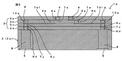
- FIGS. 5 is a cross-sectional view of the multilayer wiring board 1d
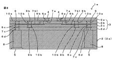
- FIG. 6 is a plan view of the multilayer wiring board 1d. In FIGS. 5 and 6, only the portion related to the present invention is shown, and the other portions are not shown.
- the laminated wiring board 1d according to this embodiment differs from the laminated wiring board 1c of the fourth embodiment described with reference to FIG. 4 in that the first via conductor 8 of the ceramic laminated body 2 is shown in FIG. A second via conductor 6d of the resin laminate 3, a via conductor 6c formed in the resin insulating layer 3c on the resin insulating layer 3d on which the second via conductor 6d is formed, and a dummy via conductor 10a. In other words, they are arranged at positions where they are superposed in plan view.
- Other configurations are the same as those of the laminated wiring board 1c of the fourth embodiment, and therefore, the description thereof is omitted by giving the same reference numerals.
- the dummy via conductor 10a is connected to the first via conductor 6b via the in-plane conductor 7b1, via conductor 6c, and in-plane conductor 7c disposed between the dummy via conductor 10a and the second via conductor 6d. It is connected to the end face (upper end face) opposite to the end face (lower end face) connected to the via conductor 8.
- the resin laminate 3 has a rectangular shape in plan view, and dummy via conductors 10a are disposed at the four corners of the rectangular resin laminate 3, respectively.
- Such an arrangement configuration of the dummy via conductors 10a can be said to be that the pair of dummy via conductors 10a arranged on the same diagonal line are arranged at point-symmetrical positions with respect to the center of the resin laminate 3 in plan view.
- FIG. 6 shows a plurality of other via conductors 11 formed inside the ceramic laminate 2 (not shown in FIG. 5).
- the other via conductors 11 and the first via conductors 8 are Each is connected to the corresponding lower surface side connection electrode 5.
- the dummy via conductor 10a is disposed at a position where it overlaps with each of the first via conductor 8 and the second via conductor 6d in plan view, and is connected to the first via conductor 8 at the end faces.
- the two via conductors 6d are connected via the via conductors 6c and the like.
- the resin laminate 3 tends to shrink from the periphery toward the center when viewed in a plan view, for example.
- the dummy via conductor 10a is disposed only in one of the four corners of the resin laminate 3 in a plan view, around the place where the dummy via conductor 10a is disposed in the resin laminate 3. While the shrinkage stress relaxation amount is large, the shrinkage stress relaxation amount around the remaining corners is small. As a result, an unbalance of the amount of relaxation of the shrinkage stress occurs in the resin laminate 3 and the warp of the laminated wiring board 1 may occur.
- the pair of dummy via conductors 10a positioned on the same diagonal line of the resin laminate 3 having a rectangular shape in plan view can be It will be arranged at a point-symmetrical position with respect to the center. Then, since the balance of the shrinkage suppression amount by each dummy via conductor 10a is improved in the resin laminate 3, the warp of the laminated wiring board 1d can be reduced.
- the shrinkage stress acts most strongly at the four corners when the resin laminate 3 contracts, and therefore the resin laminate 3 and the ceramic laminate 2.
- the interfacial peeling is likely to occur with the four corners as base points. Therefore, by disposing the dummy via conductors 10a at the four corners of the resin laminate 3, the shrinkage stress acting on the four corners is reduced, so that the interface peeling between the resin laminate 3 and the ceramic laminate 2 can be reduced. .
- FIG. 7 is a view showing a modification of the arrangement configuration of the dummy via conductors 10a, and corresponds to FIG.
- the dummy via conductors 10a are arranged only at the four corners of the rectangular resin laminate 3 in plan view.
- the dummy via conductors 10a may be arranged side by side at predetermined intervals along each side. In this way, since the dummy via conductors 10a can relieve the shrinkage stress at the time of curing shrinkage in substantially the entire region of the peripheral edge that is the base point of the interface peeling between the resin laminate 3 and the ceramic laminate 2, The effect of reducing interfacial peeling is further improved.
- the dummy via conductors 10a are arranged in a balanced manner (point-symmetric arrangement) at the peripheral edge of the resin laminate 3, it is possible to reduce the warpage of the laminated wiring board 1d.
- FIG. 8 is a cross-sectional view of the multilayer wiring board 1e. Moreover, in FIG. 8, only the part relevant to this invention is shown in figure, and the other part is abbreviate
- the laminated wiring board 1e according to this embodiment differs from the laminated wiring board 1d of the fifth embodiment described with reference to FIG. 5 in that the first via conductor 8 of the ceramic laminated body 2 is shown in FIG.
- another dummy via conductor 10b different from the dummy via conductor 10a arranged at a position overlapping in plan view is further provided. Since other configurations are the same as those of the multilayer wiring board 1d of the fifth embodiment, the description thereof is omitted by attaching the same reference numerals.
- another dummy via conductor 10b is further connected to the in-plane conductor 7b1 to which the lower end surface of the dummy via conductor 10a is connected.
- one dummy via conductor 10b is provided above and below the in-plane conductor 7b1, and both dummy via conductors 10b are arranged at positions where they overlap in plan view.
- both dummy via conductors 10b are connected to the dummy electrode pad 9b at the end surface opposite to the end surface connected to the in-plane conductor 7b1, and the dummy conductors are respectively constituted by the dummy via conductor 10b and the dummy electrode pad 9b.
- FIG. 9 is a cross-sectional view of the laminated wiring board 1f. In FIG. 9, only the part related to the present invention is shown, and the other parts are not shown.
- the laminated wiring board 1f according to this embodiment differs from the laminated wiring board 1d of the fifth embodiment described with reference to FIG. 5 in that, as shown in FIG. 9, the volume of the dummy via conductor 10a is a resin laminated body. 3 is larger than the via conductors 6a to 6d formed in the circuit board. Since other configurations are the same as those of the multilayer wiring board 1d of the fifth embodiment, the description thereof is omitted by giving the same reference numerals.
- the effect of reducing the shrinkage stress of the resin laminate 3 by the dummy via conductor 10a is improved. Therefore, the in-plane conductors 7a, 7b1, and 7b1 in the resin laminate 3 are caused by the peeling of the interface between the resin laminate 3 and the ceramic laminate 2, the warpage of the laminated wiring board 1f, and the flatness of the resin laminate 3. Each increase in the resistance value of 7c can be reduced.
- FIG. 10 is a cross-sectional view of the laminated wiring board 1g. In FIG. 10, only the parts related to the present invention are shown, and the other parts are not shown.
- the laminated wiring board 1g according to this embodiment is different from the laminated wiring board 1d of the fifth embodiment described with reference to FIG. 5 in that the area in plan view of the resin laminate 3 is as shown in FIG. It is smaller than the ceramic laminate 2. Since other configurations are the same as those of the multilayer wiring board 1d of the fifth embodiment, the description thereof is omitted by attaching the same reference numerals.
- the shrinkage stress acting on the peripheral edge of the interface which is the base point of the interface peeling between the resin laminate 3 and the semi-rack laminate 2 increases as the area of the resin laminate 3 in plan view increases. Get higher. Therefore, by making the area of the resin laminate 3 in plan view smaller than that of the ceramic laminate 2, the resin laminate 3 and the ceramic laminate 2 can be made to have the same area in plan view. Interfacial peeling between the laminate 3 and the ceramic laminate 2 can be reduced.
- FIG. 11 is a cross-sectional view of the laminated wiring board 1h. Moreover, in FIG. 11, only the part relevant to this invention is shown in figure, and the other part is abbreviate
- the laminated wiring board 1h according to this embodiment differs from the laminated wiring board 1d of the fifth embodiment described with reference to FIG. 5 in that the second via conductor 6d of the resin laminate 3 is shown in FIG.
- the lower end surface of the via conductor 8a (corresponding to the “first via conductor” of the present invention, hereinafter referred to as the first via conductor 8a) of the ceramic laminate 2 connected at the end surfaces to each other is ceramic. It is connected to the electrode pad 12 provided in the laminated body 2. Since other configurations are the same as those of the multilayer wiring board 1d of the fifth embodiment, the description thereof is omitted by giving the same reference numerals.
- the first via conductor 8 of the fifth embodiment shown in FIG. 5 is formed through the ceramic laminate 2, but in this embodiment, the length of the first via conductor 8a is short,
- the electrode pad 12 is connected to the lower end surface which is the end surface opposite to the end surface connected to the second via conductor 6d of the first via conductor 8a. Further, the electrode pad 12 and the lower surface side connection electrode 5 are arranged between the electrode pad 12 and the lower surface side connection electrode 5 by another via conductor 8b disposed at a position overlapping with the first via conductor 8a in plan view. Is connected.
- the electrode pad 12 improves the adhesion of the first via conductors 8a and 8b to the ceramic laminate 2, so that the first via conductor 8 penetrates the ceramic laminate 2 as shown in FIG. Compared with the case where it was formed, the curvature of the ceramic laminated body 2 can be reduced more.
- each multilayer wiring board 1, 1 a to 1 h is configured by the ceramic laminate 2 and the resin laminate 3 laminated on the upper surface of the ceramic laminate 2.
- the resin laminate 3 may be arranged on both the upper and lower surfaces of the ceramic laminate 2. In this way, the shrinkage stress of the resin laminate 3 on the upper surface side of the ceramic laminate 2 is offset by the shrinkage stress of the resin laminate 3 on the lower surface side, so that the warpage of the multilayer wiring board can be reduced.
- a laminated wiring board may be formed by combining the configurations of the above-described embodiments.
- the present invention can be applied to various laminated wiring boards in which a resin laminate is laminated on a ceramic laminate.
Landscapes
- Engineering & Computer Science (AREA)
- Microelectronics & Electronic Packaging (AREA)
- Physics & Mathematics (AREA)
- General Physics & Mathematics (AREA)
- Inorganic Chemistry (AREA)
- General Engineering & Computer Science (AREA)
- Chemical & Material Sciences (AREA)
- Ceramic Engineering (AREA)
- Computer Hardware Design (AREA)
- Power Engineering (AREA)
- Production Of Multi-Layered Print Wiring Board (AREA)
- Testing Or Measuring Of Semiconductors Or The Like (AREA)
- Structure Of Printed Boards (AREA)
Abstract
L'invention concerne un substrat de câblage empilé qui est obtenu par empilement d'un corps empilé en résine sur un corps empilé en céramique, ledit substrat de câblage empilé présentant un décollement réduit au niveau d'une interface entre le corps empilé en résine et le corps empilé en céramique et un gauchissement réduit du substrat de câblage empilé. Le substrat de câblage empilé (1) comprend : un corps empilé en céramique (2) obtenu par empilement d'une pluralité de couches de céramique (2a) ; et un corps empilé en résine (3) qui est obtenu par empilement d'une pluralité de couches isolantes en résine (3a à 3d) et qui est empilé sur le corps empilé en céramique (2). Dans le corps empilé en résine (3), sont formés des plots d'électrode factices (9) destinés à atténuer la contrainte due au retrait du corps empilé en résine. Par conséquent, les plots d'électrode factices (9) servent à empêcher le rétrécissement du corps empilé en résine (3) et, donc, la contrainte exercée au niveau de l'interface entre le corps empilé en céramique (2) et le corps empilé en résine (3) est réduite. Il s'ensuit que le décollement au niveau de l'interface entre le corps empilé en résine (3) et le corps empilé en céramique (2) ainsi que le gauchissement du substrat de câblage empilé peuvent être réduits.
Priority Applications (2)
| Application Number | Priority Date | Filing Date | Title |
|---|---|---|---|
| JP2015555889A JPWO2015102107A1 (ja) | 2014-01-06 | 2015-01-05 | 積層配線基板およびこれを備える検査装置 |
| US15/202,220 US20160313393A1 (en) | 2014-01-06 | 2016-07-05 | Multilayer circuit board and tester including the same |
Applications Claiming Priority (2)
| Application Number | Priority Date | Filing Date | Title |
|---|---|---|---|
| JP2014000088 | 2014-01-06 | ||
| JP2014-000088 | 2014-01-06 |
Related Child Applications (1)
| Application Number | Title | Priority Date | Filing Date |
|---|---|---|---|
| US15/202,220 Continuation US20160313393A1 (en) | 2014-01-06 | 2016-07-05 | Multilayer circuit board and tester including the same |
Publications (1)
| Publication Number | Publication Date |
|---|---|
| WO2015102107A1 true WO2015102107A1 (fr) | 2015-07-09 |
Family
ID=53493446
Family Applications (1)
| Application Number | Title | Priority Date | Filing Date |
|---|---|---|---|
| PCT/JP2015/050011 WO2015102107A1 (fr) | 2014-01-06 | 2015-01-05 | Substrat de câblage empilé et dispositif d'inspection comprenant ce dernier |
Country Status (3)
| Country | Link |
|---|---|
| US (1) | US20160313393A1 (fr) |
| JP (1) | JPWO2015102107A1 (fr) |
| WO (1) | WO2015102107A1 (fr) |
Cited By (3)
| Publication number | Priority date | Publication date | Assignee | Title |
|---|---|---|---|---|
| JPWO2015108051A1 (ja) * | 2014-01-17 | 2017-03-23 | 株式会社村田製作所 | 積層配線基板およびこれを備える検査装置 |
| JP2018190971A (ja) * | 2017-04-27 | 2018-11-29 | 京セラ株式会社 | 回路基板、プローブカードおよび回路基板用樹脂シートならびに回路基板の製造方法。 |
| JP2019079835A (ja) * | 2017-10-20 | 2019-05-23 | 日本特殊陶業株式会社 | セラミック基板 |
Families Citing this family (4)
| Publication number | Priority date | Publication date | Assignee | Title |
|---|---|---|---|---|
| TWI642335B (zh) * | 2017-12-11 | 2018-11-21 | 欣興電子股份有限公司 | 電路板及其製造方法 |
| US20200116755A1 (en) * | 2018-10-15 | 2020-04-16 | AIS Technology, Inc. | Test interface system and method of manufacture thereof |
| US11333683B2 (en) * | 2019-12-24 | 2022-05-17 | Teradyne, Inc. | Transposed via arrangement in probe card for automated test equipment |
| JP7334616B2 (ja) * | 2019-12-26 | 2023-08-29 | 住友大阪セメント株式会社 | 光導波路素子、光変調器、光変調モジュール、及び光送信装置 |
Citations (6)
| Publication number | Priority date | Publication date | Assignee | Title |
|---|---|---|---|---|
| JPH03280492A (ja) * | 1990-03-28 | 1991-12-11 | Fujitsu Ltd | 多層絶縁膜の形成方法 |
| JPH05102662A (ja) * | 1991-10-07 | 1993-04-23 | Fujitsu Ltd | 薄膜多層回路基板 |
| JPH09181445A (ja) * | 1995-12-26 | 1997-07-11 | Toppan Printing Co Ltd | プリント配線板の製造方法 |
| WO2009069398A1 (fr) * | 2007-11-30 | 2009-06-04 | Murata Manufacturing Co., Ltd. | Substrat multicouche composite en céramique, procédé de fabrication du substrat multicouche composite en céramique et composant électronique |
| JP2011108960A (ja) * | 2009-11-20 | 2011-06-02 | Kyocera Corp | 配線基板およびプローブカードならびに電子装置 |
| JP2011187830A (ja) * | 2010-03-10 | 2011-09-22 | Tdk Corp | 電子部品内蔵基板及びその製造方法 |
Family Cites Families (10)
| Publication number | Priority date | Publication date | Assignee | Title |
|---|---|---|---|---|
| US5700549A (en) * | 1996-06-24 | 1997-12-23 | International Business Machines Corporation | Structure to reduce stress in multilayer ceramic substrates |
| JP2001077543A (ja) * | 1999-09-03 | 2001-03-23 | Fujitsu Ltd | 多層配線基板 |
| JP3891766B2 (ja) * | 2000-07-27 | 2007-03-14 | 凸版印刷株式会社 | 多層フレキシブル配線基板の製造方法およびそれにより作製される多層フレキシブル配線基板 |
| JP2002319767A (ja) * | 2001-04-23 | 2002-10-31 | Toppan Printing Co Ltd | 多層プリント基板 |
| JP4239530B2 (ja) * | 2002-09-04 | 2009-03-18 | 株式会社村田製作所 | 多層セラミック基板 |
| JP4222979B2 (ja) * | 2004-07-28 | 2009-02-12 | Necエレクトロニクス株式会社 | 半導体装置 |
| JP4764731B2 (ja) * | 2006-01-30 | 2011-09-07 | 富士通株式会社 | 多層構造のプリント配線基板 |
| JP5203045B2 (ja) * | 2008-05-28 | 2013-06-05 | 日本特殊陶業株式会社 | 多層配線基板の中間製品、多層配線基板の製造方法 |
| CN202014413U (zh) * | 2008-07-14 | 2011-10-19 | 株式会社村田制作所 | 多层陶瓷基板 |
| JP2013172137A (ja) * | 2012-02-23 | 2013-09-02 | Kyocer Slc Technologies Corp | 配線基板およびそれを用いたプローブカード |
-
2015
- 2015-01-05 WO PCT/JP2015/050011 patent/WO2015102107A1/fr active Application Filing
- 2015-01-05 JP JP2015555889A patent/JPWO2015102107A1/ja active Pending
-
2016
- 2016-07-05 US US15/202,220 patent/US20160313393A1/en not_active Abandoned
Patent Citations (6)
| Publication number | Priority date | Publication date | Assignee | Title |
|---|---|---|---|---|
| JPH03280492A (ja) * | 1990-03-28 | 1991-12-11 | Fujitsu Ltd | 多層絶縁膜の形成方法 |
| JPH05102662A (ja) * | 1991-10-07 | 1993-04-23 | Fujitsu Ltd | 薄膜多層回路基板 |
| JPH09181445A (ja) * | 1995-12-26 | 1997-07-11 | Toppan Printing Co Ltd | プリント配線板の製造方法 |
| WO2009069398A1 (fr) * | 2007-11-30 | 2009-06-04 | Murata Manufacturing Co., Ltd. | Substrat multicouche composite en céramique, procédé de fabrication du substrat multicouche composite en céramique et composant électronique |
| JP2011108960A (ja) * | 2009-11-20 | 2011-06-02 | Kyocera Corp | 配線基板およびプローブカードならびに電子装置 |
| JP2011187830A (ja) * | 2010-03-10 | 2011-09-22 | Tdk Corp | 電子部品内蔵基板及びその製造方法 |
Cited By (4)
| Publication number | Priority date | Publication date | Assignee | Title |
|---|---|---|---|---|
| JPWO2015108051A1 (ja) * | 2014-01-17 | 2017-03-23 | 株式会社村田製作所 | 積層配線基板およびこれを備える検査装置 |
| JP2018190971A (ja) * | 2017-04-27 | 2018-11-29 | 京セラ株式会社 | 回路基板、プローブカードおよび回路基板用樹脂シートならびに回路基板の製造方法。 |
| JP7071201B2 (ja) | 2017-04-27 | 2022-05-18 | 京セラ株式会社 | 回路基板、プローブカードおよび回路基板の製造方法 |
| JP2019079835A (ja) * | 2017-10-20 | 2019-05-23 | 日本特殊陶業株式会社 | セラミック基板 |
Also Published As
| Publication number | Publication date |
|---|---|
| US20160313393A1 (en) | 2016-10-27 |
| JPWO2015102107A1 (ja) | 2017-03-23 |
Similar Documents
| Publication | Publication Date | Title |
|---|---|---|
| JP6304263B2 (ja) | 積層配線基板およびこれを備える検査装置 | |
| WO2015102107A1 (fr) | Substrat de câblage empilé et dispositif d'inspection comprenant ce dernier | |
| JP3904541B2 (ja) | 半導体装置内蔵基板の製造方法 | |
| JP6342120B2 (ja) | 超薄埋設ダイモジュール及びその製造方法 | |
| US8212365B2 (en) | Printed wiring board and manufacturing method thereof | |
| CN109074947B (zh) | 电子部件 | |
| JP2013243345A5 (fr) | ||
| US7923302B2 (en) | Method for manufacturing a semiconductor package | |
| WO2007049458A1 (fr) | Composant electronique empile, dispositif electronique et procede pour fabriquer le composant electronique empile | |
| WO2015151809A1 (fr) | Carte de câblage stratifiée et carte sonde la comprenant | |
| JP6531845B2 (ja) | 多層配線基板およびこれを備えるプローブカード | |
| JP6508416B2 (ja) | プローブカード用積層配線基板およびこれを備えるプローブカード | |
| US9326378B2 (en) | Thin-film wiring substrate and substrate for probe card | |
| JP6589990B2 (ja) | プローブカード用積層配線基板およびこれを備えるプローブカード | |
| JP4324732B2 (ja) | 半導体装置の製造方法 | |
| JP4480710B2 (ja) | 半導体装置内蔵基板 | |
| JP6500987B2 (ja) | 積層配線基板およびこれを備えるプローブカード | |
| JP2011009694A (ja) | 配線基板およびプローブカードならびに電子装置 | |
| JP2010038899A (ja) | セラミックプローブカードの製造方法 | |
| JP6418918B2 (ja) | プローブカード用回路基板およびそれを備えたプローブカード | |
| WO2016114170A1 (fr) | Carte de sondage et carte de câblage multicouche dont ladite carte de sondage est munie | |
| JPH11274372A (ja) | 半導体装置及びその半導体パッケージ | |
| JP7438656B2 (ja) | 集合基板 | |
| JP6887862B2 (ja) | 有機回路基板、回路基板およびプローブカード | |
| JP5089660B2 (ja) | 半導体装置内蔵基板の製造方法 |
Legal Events
| Date | Code | Title | Description |
|---|---|---|---|
| 121 | Ep: the epo has been informed by wipo that ep was designated in this application |
Ref document number: 15733212 Country of ref document: EP Kind code of ref document: A1 |
|
| ENP | Entry into the national phase |
Ref document number: 2015555889 Country of ref document: JP Kind code of ref document: A |
|
| NENP | Non-entry into the national phase |
Ref country code: DE |
|
| 122 | Ep: pct application non-entry in european phase |
Ref document number: 15733212 Country of ref document: EP Kind code of ref document: A1 |