WO2015037252A1 - 発振回路、それを用いた半導体集積回路装置および回転角検出装置 - Google Patents
発振回路、それを用いた半導体集積回路装置および回転角検出装置 Download PDFInfo
- Publication number
- WO2015037252A1 WO2015037252A1 PCT/JP2014/052389 JP2014052389W WO2015037252A1 WO 2015037252 A1 WO2015037252 A1 WO 2015037252A1 JP 2014052389 W JP2014052389 W JP 2014052389W WO 2015037252 A1 WO2015037252 A1 WO 2015037252A1
- Authority
- WO
- WIPO (PCT)
- Prior art keywords
- terminal
- capacitor
- circuit
- oscillation
- output
- Prior art date
- Legal status (The legal status is an assumption and is not a legal conclusion. Google has not performed a legal analysis and makes no representation as to the accuracy of the status listed.)
- Ceased
Links
Images


Classifications
-
- G—PHYSICS
- G01—MEASURING; TESTING
- G01C—MEASURING DISTANCES, LEVELS OR BEARINGS; SURVEYING; NAVIGATION; GYROSCOPIC INSTRUMENTS; PHOTOGRAMMETRY OR VIDEOGRAMMETRY
- G01C19/00—Gyroscopes; Turn-sensitive devices using vibrating masses; Turn-sensitive devices without moving masses; Measuring angular rate using gyroscopic effects
- G01C19/56—Turn-sensitive devices using vibrating masses, e.g. vibratory angular rate sensors based on Coriolis forces
- G01C19/5776—Signal processing not specific to any of the devices covered by groups G01C19/5607 - G01C19/5719
-
- H—ELECTRICITY
- H03—ELECTRONIC CIRCUITRY
- H03K—PULSE TECHNIQUE
- H03K3/00—Circuits for generating electric pulses; Monostable, bistable or multistable circuits
- H03K3/02—Generators characterised by the type of circuit or by the means used for producing pulses
- H03K3/023—Generators characterised by the type of circuit or by the means used for producing pulses by the use of differential amplifiers or comparators, with internal or external positive feedback
- H03K3/0231—Astable circuits
-
- H—ELECTRICITY
- H03—ELECTRONIC CIRCUITRY
- H03K—PULSE TECHNIQUE
- H03K4/00—Generating pulses having essentially a finite slope or stepped portions
- H03K4/06—Generating pulses having essentially a finite slope or stepped portions having triangular shape
Definitions
- the oscillation circuit of (1) above is Based on the first timing (D), the terminal voltage of the first capacitor (C1) is pulled down or pulled up in the second direction, and the terminal voltage of the second capacitor (C3) is pulled in the first direction. Up or down.
- the oscillation circuit of (2) above is A third capacitor (C2) that is charged and driven by current and whose terminal voltage changes linearly in the first direction; A fourth capacitor (C4) which is driven to discharge by current together with the charge driving of the third capacitor and whose terminal voltage linearly changes in the second direction; Comprising The oscillation output is inverted based on the second timing (C, C ′) at which the terminal voltages of the third and fourth capacitors (C2, C4) intersect.
- a second short circuit (M12) A third capacitor (C2) having first and second terminals, the first terminal being connected to a reference potential; A third constant current source (M9) provided between the second terminal (N2) of the third capacitor (C2) and the first power supply terminal (VD1); A third short circuit (M11) for short-circuiting between the second terminal (N2) of the third capacitor (C2) and the reference potential based on the second control signal; A fourth capacitor (C4) having first and second terminals, the first terminal being connected to a reference potential; A fourth constant current source (M15) provided between the second terminal (N4) of the fourth capacitor (C4) and the reference potential; A fourth short circuit (M13) for short-circuiting between the second terminal (N4) of the fourth capacitor (C4) and the first power supply terminal (VD1) based on the first control signal; A first comparator (CMP1, CMP3) for comparing the second terminal potential of the first capacitor (C1) and the second terminal potential of the second capacitor (C3); A second comparator (CMP2, CMP4)
- Example 1 is an oscillation circuit that forms an oscillation period by using a capacitor charging time with a constant current, and suppresses fluctuations in the oscillation period due to temperature fluctuations, and is relatively several tens of MHz (about 20 MHz to 60 MHz). It is an object of the present invention to provide an oscillation circuit that can ensure the oscillation frequency accuracy even in a high frequency region.
- FIG. 1 is a circuit diagram illustrating a configuration of the oscillation circuit according to the first embodiment.
- FIG. 2 is a waveform diagram illustrating the operation of the oscillation circuit according to the first embodiment.
- the oscillation circuit 10A according to the first embodiment includes a constant current generation circuit 1, a comparison reference voltage generation circuit 2, and an oscillation circuit core unit OSC1.
- the constant current generation circuit 1 includes a PMOS transistor M1, an operational amplifier (differential amplifier) A1, and a resistor R1. In the PMOS transistor M1, its drain terminal is connected to GND via the resistor R1, and its source terminal is connected to the power supply terminal VCC.
- the logic circuit L1 has a set signal input terminal S, a reset signal input terminal R, an output terminal Q, and an inverted output terminal QB. The logic circuit L1 outputs a high level signal to the output terminal Q during a period from when the rising edge is input to the set signal input terminal S to when the rising edge is input to the reset signal input terminal R, and is reset.
- a low level signal is output to the output terminal Q.
- the logic circuit L1 outputs a signal having a polarity obtained by inverting the signal output from the output terminal Q to the inverting output terminal QB.
- the non-inverting input terminal (+) is connected to the connection point (node N1) between the capacitor C1 and the drain terminal of the PMOS transistor M3, the inverting input terminal ( ⁇ ) is output to the output terminal VR, and the output is output to the logic circuit L1.
- each of the capacitor C1 and the capacitor C2 is connected to the GND.
- the present invention is not limited to this.
- the capacitor C1 and the capacitor C2 may be connected to the power supply terminal VCC instead of the GND.
- connection order of the inverting input ( ⁇ ) and the non-inverting input (+) of the comparators CMP1 and CMP2, and the signal polarity of the set signal input terminal S and the reset signal input terminal R of the logic circuit L1 are also configured for convenience of explanation.
- the present invention is not limited to this configuration as long as an operation function described below can be obtained.
- the current value of the current I1 is a constant current that does not depend on the voltage applied to the power supply terminal VCC, as is apparent from the equation (1). Since the PMOS transistor M2 in the comparison reference voltage generation circuit 2 is in a current mirror relationship with the PMOS transistor M1 in the constant current generation circuit 1, the drain current I2 of the PMOS transistor M2 is also a constant current. Therefore, the potential drop of the resistor R2 is also a constant voltage. That is, a constant comparison reference voltage is output to the output terminal VR.
- ⁇ is a mirror ratio between the PMOS transistor M1 and the PMOS transistor M2.
- the PMOS transistor M3 and the PMOS transistor M4 also have a current mirror relationship with the PMOS transistor M1 in the constant current generation circuit 1, so that they function as a constant current source.
- ⁇ is a mirror ratio of the PMOS transistor M1, the PMOS transistor M3, and the PMOS transistor M4.
- the NMOS transistor M6 transitions to the ON state, short-circuits both terminals of the capacitor C2, and the capacitor C2 is discharged.
- the potential of the terminal (node N2) of the capacitor C2 that has been charged by the drain current I4 of the PMOS transistor M4 until just before is lowered toward GND (0 V) as shown in FIG. become.
- the output of the comparator CMP1 is inverted to the high level, the high level is output to the inversion output terminal QB of the logic circuit L1, thereby maintaining the on state of the NMOS transistor M6.
- the potential of the terminal of the capacitor C2 (node N2) is substantially fixed at GND.
- the output of the comparator CMP1 and the output of the logic circuit L1 are inverted after the potential of the terminal (node N1) of the capacitor C1 reaches the comparison reference voltage (V R ).
- V R comparison reference voltage
- td1 A certain finite delay time is required.
- the response of the logic circuit L1 generally composed of a CMOS logic gate or the like is sufficiently faster than the response of the comparator CMP1, so that most of the delay time (td1) occupies the response time of the comparator CMP1.
- the comparator CMP2 has the same circuit configuration as the comparator CMP1. Also, it is assumed that the PMOS transistor constants are set such that the drain currents I3 and I4 of the PMOS transistor M3 and the PMOS transistor M4 are the same current. By doing so, the delay similar to that on the comparator CMP1 side until the output of the comparator CMP2 and the output of the logic circuit L1 are inverted after the potential of the terminal (node N2) of the capacitor C2 reaches the comparison reference voltage (V R ). Time (td2) is required.
- the NMOS transistor M5 transitions to the OFF state in response to the inversion of the output terminal Q of the logic circuit L1 to the low level, and the drain current I3 of the PMOS transistor M3 again causes the capacitor Charging of C1 is started.
- the state is equivalent to the state of timing A. Thereafter, the operations of charging the capacitor C1 and shorting the capacitor C2, and shorting the capacitor C1 and charging the capacitor C2 as described above are repeated alternately. Become.
- the oscillation period (T) is changed from the comparator CMP1 output inversion on the capacitor C1 side to the next comparator CMP1 output inversion, or the capacitor C2. This corresponds to the period from the inversion of the comparator CMP2 output to the next comparator CMP2 output inversion.
- the charging period (Tc2) of the capacitor C2 + the delay time (td2) represents the half period of the oscillation period (T), and the charging period (Tc1) of the capacitor C1.
- the remaining half cycle is formed by the + delay time (td1), and the discharge time due to the short circuit of the capacitor C1 and the capacitor C2 by the NMOS transistor M5 and the NMOS transistor M6 does not affect the oscillation cycle (T).
- the capacitors C1 and C2 have the same capacitance, the PMOS transistor M3 and the PMOS transistor M4 are set to the same constant, and the comparators CMP1 and CMP2 are configured by the same circuit, the capacitors The charging period (Tc1) of C1 and the charging period (Tc2) of the capacitor C2 are substantially equal, and the delay time (td1) related to the output inversion of the comparator CMP1 and the delay time (td2) related to the output inversion of the comparator CMP2 are almost the same.
- the capacitance value of the capacitor C1 (and capacitor C2) is C
- T C C ⁇ V R / I 3 (4)
- the time component related to the discharge can be prevented from affecting the oscillation cycle, and therefore, even in a relatively high frequency region. Oscillation cycle fluctuations with respect to parameter fluctuations such as temperature fluctuations can be suppressed, and an oscillation circuit superior in ensuring oscillation frequency accuracy can be obtained.
- an oscillation pulse with a duty of approximately 50% can be obtained.
- the duty of the oscillation pulse refers to the ratio of the high level period of the oscillation pulse to the oscillation period (T).
- the oscillation period can be obtained without depending on the voltage of the reference voltage input terminal VREF, for example, some reference voltage output such as a band gap circuit configured on the same semiconductor substrate is used. Even in this case, even if the reference voltage output varies or varies due to temperature, the influence can be canceled, so that an oscillation circuit suitable for ensuring the oscillation frequency accuracy can be obtained.
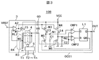
- FIG. 3 is a circuit diagram showing a configuration of an oscillation circuit according to the first modification.
- the oscillation circuit 10B according to the first modification is obtained by replacing the constant current generation circuit 1 and the comparison reference voltage generation circuit 2 of the oscillation circuit 10A according to the first embodiment with a bias circuit 3. That is, the oscillation circuit core part of the oscillation circuit 10B has the same configuration as the oscillation circuit core part OCS1 of the oscillation circuit 10A. However, the bias output terminal G0 to which the gate terminals of the PMOS transistor M3 and the PMOS transistor M4 are connected and the output terminal VR for sending the comparison reference voltage VR are both provided by the bias circuit 3.
- the bias circuit 3 includes a ladder resistor RL2, a PMOS transistor M7, an operational amplifier A2, an analog switch circuit 4, and a decoder circuit 5.
- the bias circuit 3 has functions of a constant current generation circuit and a reference voltage generation circuit.
- the ladder resistor RL2, the analog switch circuit 4, and the decoder circuit 5 constitute a trimming circuit that adjusts the reference voltage value. That is, the bias circuit 3 has a reference voltage trimming function.
- the ladder resistor RL2 is configured such that a plurality of unit resistors are connected in series and one end of the lowest unit resistor is connected to the GND so that a divided voltage output can be taken out from an arbitrary connection point of each unit resistor.
- the analog switch circuit 4 selectively sends each divided output of the ladder resistor RL2 to the output terminal VR.
- the decoder circuit 5 controls on / off of each switch in the analog switch circuit 4 in accordance with the n-bit frequency trimming signal input terminals T1 to Tn and the input signals of the frequency trimming signal input terminals T1 to Tn.
- the current I5 is a constant current that does not depend on the voltage applied to the power supply terminal VCC, like the current I1 of the first embodiment.
- any one of the switches in the analog switch circuit 4 is selectively turned on to the output terminal VR by the input signals of the frequency trimming signal input terminals T1 to Tn, and the output of the ladder resistor RL2 to which the selected switch is connected. Pressure output is delivered.
- the voltage sent to the output terminal VR becomes a comparison reference voltage for the comparators CMP1 and CMP2, and determines the charging time (T C ) of the capacitors C1 and C2.
- the oscillation operation of this modification uses the charging time of the capacitor C1 and the capacitor C2 by the PMOS transistor M3 and the PMOS transistor M4.
- the outline of the operation is shown in the waveform diagram of FIG. It is the same as that.
- T C The charging time (T C ) of the capacitor C1 is expressed by the equation (4).
- ⁇ represents the mirror ratio between the PMOS transistor M7 and the PMOS transistor M3.
- the oscillation period (T) is calculated by assuming that the response delay time of the comparators CMP1 and CMP2 is td.
- an oscillation circuit that can adjust the oscillation frequency can be obtained.
- the functions related to the frequency trimming input signal terminals T1 to Tn shown in the present embodiment are not limited to the configuration of the present embodiment, and are provided in, for example, the comparison reference voltage generation circuit 2 in the first embodiment of FIG. Is also possible.
- the resistor R2 may be configured in the form of a ladder resistor.
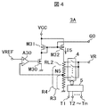
- FIG. 4 is a diagram illustrating a configuration of a bias circuit according to the second modification. Also, the configuration of the bias circuit 3 is not limited to the configuration shown in FIG. 3, and may be configured as shown in FIG. 4, for example.
- the PMOS transistor M32 its source terminal is connected to the power supply terminal VCC, and its gate terminal is connected to the gate terminal of the PMOS transistor M31 to form a current mirror with the PMOS transistor M31.
- the ladder resistor RL2 a plurality of unit resistors are connected in series, one end of the uppermost unit resistor is connected to the drain terminal of the PMOS transistor M32, and one end of the lowermost unit resistor is connected to the GND.
- the partial pressure output can be taken out from the point.
- the analog switch circuit 4 selectively sends each divided output of the ladder resistor to the output terminal VR.
- the decoder circuit 5 controls on / off of each switch in the analog switch circuit 4 in accordance with the n-bit frequency trimming signal input terminals T1 to Tn and the input signals of the frequency trimming signal input terminals T1 to Tn.
- the non-inverting input terminal (+) is connected to the reference voltage input terminal VREF
- the inverting input terminal ( ⁇ ) is an arbitrary divided output of the ladder resistor and the resistance value viewed from GND is R 3
- the output terminal is connected to the point (node N5) to the gate terminal of the NMOS transistor M30.
- FIG. 5 is a circuit diagram illustrating a configuration of the oscillation circuit according to the second embodiment.
- FIG. 6 is a waveform diagram showing the operation of the oscillation circuit.
- the oscillation circuit 10C includes a power supply terminal VD1, a constant current bias source IB0, and an oscillation circuit core unit OSC2.
- the oscillation circuit core unit OSC2 includes a PMOS transistor M16, a PMOS transistor M17, and an NMOS transistor M18.
- the source terminal is connected to the power supply terminal VD1
- the drain terminal is connected to the constant current bias source IB0
- the gate terminal and the drain terminal are short-circuited.
- the PMOS transistor M17 its source terminal is connected to the power supply terminal VD1
- its gate terminal is connected to the gate terminal of the PMOS transistor M16.
- the oscillation circuit core unit OSC2 includes PMOS transistors M8 and M9, NMOS transistors M14 and M15, and capacitors C1, C2, C3, and C4.
- PMOS transistor M8 and M9 In the PMOS transistor M8, its drain terminal is connected to the capacitor C1, its source terminal is connected to the power supply terminal VD1, and its gate terminal is connected to the gate terminal of the PMOS transistor M16.
- PMOS transistor M9 In the PMOS transistor M9, its drain terminal is connected to the capacitor C2, its source terminal is connected to the power supply terminal VD1, and its gate terminal is connected to the gate terminal of the PMOS transistor M16.
- NMOS transistor M14 In the NMOS transistor M14, its drain terminal is connected to the capacitor C3, its source terminal is connected to GND, and its gate terminal is connected to the gate terminal of the NMOS transistor M18.
- NMOS transistor M15 In the NMOS transistor M15, its drain terminal is connected to the capacitor C4, its source terminal is connected to GND, and its gate terminal is connected to the gate terminal of the NMOS transistor M18.
- the oscillation circuit core unit OSC2 includes NMOS transistors M10 and M11, PMOS transistors M12 and M13, a logic circuit L1, a comparator CMP1, and a comparator CMP2.
- NMOS transistor M10 its drain terminal is connected to the drain terminal of the PMOS transistor M8, its source terminal is connected to GND, and its gate terminal is connected to the output terminal Q of the logic circuit L1.
- NMOS transistor M11 its drain terminal is connected to the drain terminal of the PMOS transistor M9, its source terminal is connected to GND, and its gate terminal is connected to the inverting output terminal QB of the logic circuit L1.
- the non-inverting input terminal (+) is connected to the connection point (node N1) between the drain terminal of the PMOS transistor M8 and the capacitor C1
- the inverting input terminal ( ⁇ ) is connected to the drain terminal of the NMOS transistor M14 and the capacitor C3.
- the non-inverting input terminal (+) is connected to the connection point (node N2) between the drain terminal of the PMOS transistor M9 and the capacitor C2, and the inverting input terminal ( ⁇ ) is connected to the drain terminal of the NMOS transistor M15 and the capacitor C4.
- the reset signal input terminal R of the logic circuit L1 is connected to the reset signal input terminal R of the logic circuit L1.
- the output terminal Q of the logic circuit L1 is connected to the oscillation output terminal OUT.
- the oscillation output may be taken out from the output terminal QB of the logic circuit L1.
- a signal output from the output terminal Q is referred to as a first control signal
- a signal output from the output terminal QB is referred to as a second control signal.
- FIG. 6A shows the potentials of the terminals of the capacitors C1 and C3 (nodes N1 and N3)
- FIG. 6B shows the potential of the terminals of the capacitors C2 and C4 (nodes N2 and N4)
- FIG. 6C shows the potential of the comparator CMP1.
- D is the output voltage of the comparator CMP2
- e is the voltage at the output terminal Q (oscillation output terminal OUT) of the logic circuit L1
- (f) is the inverted output of the logic circuit L1.
- the voltage at the terminal QB is shown.
- V D1 a constant voltage
- IB0 the current I6 flowing through the PMOS transistor M16 by the constant current bias source IB0
- the currents I8 and I9 flowing in the PMOS transistor M8 and the PMOS transistor M9, which are in a current mirror relationship with the PMOS transistor M16 are constant currents.
- the current I7 flowing through the PMOS transistor M17 that is in a current mirror relationship with the PMOS transistor M16 is a constant current.
- the NMOS transistor M10 and the NMOS transistor M11 have a current driving capability that is sufficiently larger than the currents I8 and I9 from the PMOS transistor M8 and the PMOS transistor M9. It is assumed that the terminal (node N1) and the terminal of the capacitor C2 (node N2) are short-circuited to GND, and the potential of these terminals (nodes N1 and N2) can be pulled down to almost GND.
- the PMOS transistor M12 and the PMOS transistor M13 also have a current driving capability that is sufficiently larger than the currents I10 and I11 in the NMOS transistor M14 and NMOS transistor M15.
- capacitors C1, C2, C3, and C4 are set to have the same capacitance value C, and currents I8, I9, I10, and I11 are set to have the same current value. To do.
- both the NMOS transistor M10 and the PMOS transistor M12 are in the ON state, so that the potential of the terminal of the capacitor C1 (node N1) is almost GND (0 V) and the terminal potential of the capacitor C3. Is substantially fixed at V D1 .
- the capacitor C1 starts to be charged with the current I8, and its terminal voltage rises linearly toward V D1 .
- the discharge by the current I10 is started from that time, and the potential of the terminal (node N1) decreases linearly toward GND (0V).
- “decreasing linearly” means that the decrease time between the predetermined potentials is substantially constant.
- charging is a bias application in the direction in which the potential difference between both terminals of the capacitor is expanded, and discharging is only a bias application in a direction in which the potential difference between both terminals of the capacitor is reduced.
- the relationship between the capacitor and the charge / discharge operation of each capacitor is not limited to the description of this embodiment. For example, if one end of the capacitor C1 is connected to the power supply terminal VD1 instead of GND, the capacitor C1 is “discharged” by the current I8, and the terminal voltage rises linearly toward V D1. .
- the NMOS transistor M11 which is a short circuit of the capacitor C2 has its gate terminal transitioned to the high level and turned on, and the PMOS transistor M13 which is a short circuit of the capacitor C4 is The gate terminal transitions to the low level and also transitions to the on state. Therefore, after timing C, the terminal of the capacitor C2 (node N2) is pulled down to GND, and the terminal of the capacitor C4 (node N4) is pulled up to V D1 .
- the potential of the terminal of the capacitor C1 (node N1) and the potential of the terminal of the capacitor C3 (node N3) Since the time required to transition to 1/2 voltage of V D1 is equal, the potential of the terminal of the capacitor C1 (node N1) and the potential of the terminal of the capacitor C3 (node N3) are respectively set to 1/2 voltage of V D1. It will cross when it reaches.
- the non-inverting input terminal (+) side of the comparator CMP1 is lower than the inverting input terminal ( ⁇ ) side. For this reason, the output of the comparator CMP1 outputs a low level.
- the comparator CMP1 passes through the response delay time (td1 ′) of the comparator CMP1 from the time when the potential of the terminal of the capacitor C1 (node N1) and the potential of the terminal of the capacitor C3 (node N3) cross, that is, the same potential. The output is inverted to the high level. This corresponds to the state of timing D in FIG.
- the potentials of the terminals are substantially fixed to GND and V D1 by the respective short-circuit circuits of the NMOS transistor M11 and the PMOS transistor M13.
- the capacitor C2 starts to be charged with the current I9, and the potential of the terminal of the capacitor C2 (node N2) goes from GND (0V) to V D1 .
- the capacitor C4 starts discharging with the current I11, and the potential of the terminal of the capacitor C4 (node N4) decreases linearly from V D1 to GND (0 V). If the current I9 and the current I11 have the same current value, the terminals of the capacitors C2 and C4 (nodes N2 and N4) with a voltage of 1/2 of V D1 as in the case of the capacitors C1 and C3 after the timing C. Will cross each other.
- the comparator CMP2 receives the response delay time (td2) as in the case of the comparator CMP1. After that, the output is inverted to High level. This corresponds to the timing C ′ in FIG.
- (C) Timing C ′ At this timing C ′, when the output of the comparator CMP2 is inverted to the high level and the inverted output terminal QB side of the logic circuit L1 transitions to the high level and the output terminal Q side transitions to the low level, the NMOS transistor M10 and the PMOS transistor M12 are turned off. After the transition to the state, charging of the capacitor C1 and discharging of the capacitor C3 by the currents I8 and I10 are started again.
- the NMOS transistor M11 and the PMOS transistor M13 are turned on, the capacitor C2 terminal (node N2) is pulled down to GND, and the capacitor C4 terminal (node N4) is pulled up to V D1 , thereby the terminal of the capacitor C2 ( The potential of the terminal of the capacitor C4 (node N4) with respect to the potential of the node N2) rises rapidly, and the output of the comparator CMP2 returns to the low level.
- This state is equivalent to the state at the timing C described above, and the operation described above is repeated thereafter.
- the oscillation output terminal OUT is taken out from the output terminal Q of the logic circuit L1, and the period from the inversion of the comparator CMP1 output (or the comparator CMP2 output) to the high level until the inversion to the next high level is the oscillation period (T ).
- the High period and Low period of the output terminal Q are formed by the time related to charging / discharging of the capacitor C1 / capacitor C3 and the time related to charging / discharging of the capacitor C2 / capacitor C4, respectively.
- the time width can be set, and therefore, an oscillation pulse of approximately 50% duty can be obtained.
- the response delay times (td ′) of the comparators CMP1 and CMP2 in order for each comparator output to invert to the high level, the terminal potential on the non-inverting input terminal (+) side must be on the inverting input terminal ( ⁇ ) side. It is necessary to exceed the terminal potential, and the larger the potential difference between them, the shorter the response delay time until output inversion.
- the potential of the terminal (node N1) of the capacitor C1 that is rising due to charging (or the potential of the terminal of the capacitor C2 (node N2)) and the terminal of the capacitor C3 that is falling due to discharging (node N3) Since the configuration is such that the potential (or the potential of the terminal of the capacitor C4 (node N4)) is compared, the input potential difference is more compared to the case where the comparison is made with a constant comparison reference voltage (V R ) as in the first embodiment. It can be expanded early, and the response delay time (td ′) can be shortened.
- td which is a component related to the response delay time of the comparator in the expressions (6) and (10) representing the oscillation period (T) described in the first embodiment and the first modification, is compressed, and the comparator changes due to parameter fluctuations such as temperature fluctuations. Even if the response delay time fluctuates, since the ratio of td in the oscillation period (T) can be reduced, the fluctuation of the oscillation frequency can be suppressed as compared with the first embodiment.
- the response delay time of the comparator can be shortened, it is possible to obtain an oscillation circuit that is superior in ensuring the oscillation frequency accuracy.
- the PMOS transistors M8 and M9 and the NMOS transistors M14 and M15 constituting the constant current sources for driving the capacitors C1 and C2 to charge and driving the capacitors C3 and C4 to discharge are all connected to the capacitor terminals (nodes N1, N2, N3, N3,. Because of the configuration directly connected to N4), when any of the NMOS transistors M10 and M11 and the PMOS transistors M12 and M13 constituting the short circuit switch is turned on, the output current of the constant current source is in the on state. Bypass to the short-circuit switch side. Since this is a reactive current, it is originally advantageous to cut it off from the viewpoint of current consumption. However, if a configuration that cuts off this is used, the following problems occur.
- a cut-off switch is provided between the drain terminal of the PMOS transistor M8 and the terminal (node N1) of the capacitor C1, and the NMOS transistor is a short-circuit switch.
- the cutoff switch is turned off when M10 is turned on. This can be easily realized by providing a PMOS transistor as the cutoff switch and directly connecting the gate terminal to the gate terminal of the NMOS transistor M10.
- the NMOS transistor M10 is turned off and at the same time the cutoff switch is turned on. At that moment, the charge charged in the parasitic capacitance is changed. Distribution to the capacitor C1 side (so-called charge sharing occurs) changes the potential of the terminal (node N1) of the capacitor C1. As a result, the detection timing by the comparator CMP1 varies, and the oscillation period varies.
- the present embodiment and other embodiments also employ a configuration capable of suppressing oscillation frequency fluctuations due to the charge share as a configuration in which a constant current source is directly connected to each capacitor.
- the terminal voltages of the charge drive side capacitor and the discharge drive side capacitor that are driven simultaneously are compared with each other to be compared with a constant comparison reference voltage (V R ).
- V R a constant comparison reference voltage
- the comparator detection timing period must be the same in order to obtain the same oscillation period, so whether the voltage amplitude itself during charge (or discharge) drive should be doubled after doubling the capacitor drive current
- the comparison reference voltage (V R ) is used as the voltage (or GND voltage) of the power supply terminal VD1, and the voltage change width within the comparator detection timing cycle is doubled.
- V R a constant comparison reference voltage
- Modification 3 provides an oscillation circuit that can adjust the oscillation frequency and is more advantageous for ensuring the oscillation frequency accuracy.
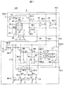
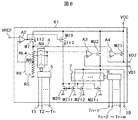
- FIG. 7 is a circuit diagram showing a configuration of an oscillation circuit according to the third modification.
- the oscillation circuit core unit OSC3 of the oscillation circuit 10D according to Modification 3 has the same configuration as that of the oscillation circuit core unit OSC2 of the oscillation circuit 10C of Example 2 except for the logic circuit L2, the comparator CMP3, and the comparator CMP4.
- the oscillation circuit 10 ⁇ / b> D has a bias circuit 6. The difference between the oscillation circuit 10D and the oscillation circuit 10C will be described below.
- the bias circuit 6 has a power supply terminal VCC, a reference voltage input terminal VREF, and output terminals IB, VD1, and VD2.
- the inverting input terminal ( ⁇ ) is connected to the connection point (node N1) between the drain terminal of the PMOS transistor M8 and the capacitor C1, and the non-inverting input terminal (+) is connected to the drain terminal of the NMOS transistor M14 and the capacitor C3.
- the inverting input terminal ( ⁇ ) is connected to the connection point (node N2) between the drain terminal of the PMOS transistor M9 and the capacitor C2, and the non-inverting input terminal (+) is connected to the drain terminal of the NMOS transistor M15 and the capacitor C4.
- the output terminal Q of the logic circuit L2 is connected to the oscillation output terminal OUT. The oscillation output may be taken out from the output terminal QB of the logic circuit L2.
- the bias circuit 6 includes a ladder resistor RL4, a PMOS transistor M7, an operational amplifier A2, an analog switch circuit 4, a decoder circuit 5, a PMOS transistor M19, an NMOS transistor M20, an NMOS transistor M21, an operational amplifier A3, and a PMOS.
- the transistor M22, the operational amplifier A4, and the PMOS transistor M23 are included.
- the bias circuit 6 has the functions of a constant current generation circuit and a reference voltage generation circuit, like the bias circuit 3.
- the ladder resistor RL4, the analog switch circuit 4, and the decoder circuit 5 constitute a trimming circuit that adjusts the reference voltage value. That is, the bias circuit 6 has a reference voltage trimming function.
- the ladder resistor RL4 a plurality of unit resistors are connected in series and one end of the lowermost unit resistor is connected to the GND so that a divided voltage output can be taken out from an arbitrary connection point of each unit resistor.
- the PMOS transistor M7 its drain terminal is connected to one end (node N8) of the uppermost unit resistor of the ladder resistor RL4, and its source terminal is connected to the power supply terminal VCC.
- the inverting input terminal ( ⁇ ) is the reference voltage input terminal VREF
- the non-inverting input terminal (+) is an arbitrary divided output of the ladder resistor RL4, and the resistance value viewed from GND is R 5 .
- the output terminal is connected to the connection point (node N6) to the gate terminal of the PMOS transistor M7.
- the operational amplifiers A2, A3, and A4 operate between the potential of the power supply terminal VCC and GND.
- the analog switch circuit 4 selectively outputs each divided voltage output of the ladder resistor RL4.
- the decoder circuit 5 controls on / off of each switch in the analog switch circuit 4 according to the input signals of the n-bit frequency trimming signal input terminals T1 to Tn and the frequency trimming signal input terminals T1 to Tn. .
- the source terminal is connected to the power supply terminal VCC and the gate terminal is connected to the output terminal of the operational amplifier A2, and the PMOS transistor M7 and the current mirror are in a relationship.
- NMOS transistor M20 In the NMOS transistor M20, its drain terminal is connected to the drain terminal of the PMOS transistor M19, its source terminal is connected to GND, and its gate terminal is short-circuited to the drain terminal.
- the drain terminal In the NMOS transistor M21, the drain terminal is connected to the output terminal IB, the source terminal is connected to GND, the gate terminal is connected to the gate terminal of the NMOS transistor M20, and the NMOS transistor M20 has a current mirror relationship.
- operational amplifier A3 In the operational amplifier A3, its inverting input terminal ( ⁇ ) is connected to the output of the analog switch circuit 4, and its non-inverting input terminal (+) is connected to the output terminal VD1.
- the PMOS transistor M22 its source terminal is connected to the power supply terminal VCC, its drain terminal is connected to the output terminal VD1, and its gate terminal is connected to the output terminal of the operational amplifier A3.
- the inverting input terminal ( ⁇ ) is connected to the connection point between the drain terminal of the PMOS transistor M7 and the uppermost unit resistor of the ladder resistor RL4, and the non-inverting input terminal (+) is connected to the output terminal VD2.
- the PMOS transistor M23 its source terminal is connected to the power supply terminal VCC, its drain terminal is connected to the output terminal VD2, and its gate terminal is connected to the output terminal of the operational amplifier A4.
- the logic circuit L2 includes a NAND gate G1, a NAND gate G2, an inverter G3, and an inverter G4.
- NAND gate G1 one of its input terminals is connected to the set signal input terminal S, and its output terminal is connected to the input terminal of the inverter G3.
- NAND gate G2 one of its input terminals is connected to the reset signal input terminal R, the other input terminal is connected to the output terminal of the NAND gate G1, and its output terminal is connected to the other input terminal of the NAND gate G1.
- the inverter G4 has its input terminal connected to the output terminal of the inverter G3, the output terminal of the inverter G3 is the inverted output terminal QB, and the output terminal of the inverter G4 is the output terminal Q.
- the logic circuit L2 outputs a high level signal to the output terminal Q during a period from when the falling edge is input to the set signal input terminal S to when the falling edge is input to the reset signal input terminal R.
- the logic circuit L2 outputs a low level signal to the output terminal Q during a period from when the falling edge is input to the reset signal input terminal R to when the falling edge is input to the set signal input terminal S.
- a signal having a polarity obtained by inverting the signal output of the output terminal Q is output to the inverted output terminal QB.
- a signal output from the output terminal Q is referred to as a first control signal
- a signal output from the output terminal QB is referred to as a second control signal.
- the source terminals of the PMOS transistors M8, M9, M12, M13, M16, and M17 are connected to the output terminal VD1 of the bias circuit 6, and the power supplies of the comparators CMP3 and CMP4 and the logic circuit L2 are output.
- the configuration is given from the terminal VD2. Providing two power sources in this way is not necessarily an essential matter, but its unique effect will be described in the following description of the operation.
- the charge / discharge time (T C ′) is expressed in a form that does not include the components of voltage (V D1 ) and constant current (I 6 ), but this is the voltage (V D1 ).
- the constant current (I 6 ) are in a constant proportional relationship as shown in the equation (14), and when it fluctuates with a component that does not depend on the proportional relationship, such as the above-described voltage fluctuation, discharge time (T C ') also it would lead to variation.
- the fluctuation of the charge / discharge time (T C ′) leads to the fluctuation of the oscillation period (T).
- T oscillation period
- Each of the output terminals VD1 of the bias circuit 6 according to the present modification is connected to the power supply terminal VD1 of the oscillation circuit 10C according to the second embodiment, and the output terminal IB of the bias circuit 6 is replaced with the constant current bias source IB0 to replace the PMOS transistor
- An oscillation circuit may be configured by connecting to the drain terminal of M16.
- the current mirror ratio with the NMOS transistor M20 may be effectively changed by changing the selection number of the collector terminals of the NMOS transistors M211 to M21i according to the input signals of the frequency trimming signal input terminals Tn + 1 to Tn + m.
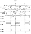
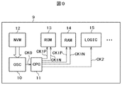
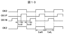
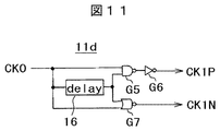
- FIG. 10 is a timing chart of the clock pulse generation circuit according to the third embodiment.
- the two-phase clock signals CK1P and CK1N have a delay time (tcd) on the rising side with respect to the oscillation output signal CK0 as described above.
- a two-phase clock signal is formed without overlapping the periods.
- the access control of the RAM module 14 is performed using the two-phase clock signals CLK1P and CLK1N, for example, the high-level period of the two-phase clock signal CK1P is set to the data line precharge in the RAM module 14. It is possible to perform read control such that the high-level period of the two-phase clock signal CK1N is allocated to the activation of the data read sense amplifier and the latch control of the sense amplifier output data.
Landscapes
- Engineering & Computer Science (AREA)
- Signal Processing (AREA)
- Physics & Mathematics (AREA)
- General Physics & Mathematics (AREA)
- Radar, Positioning & Navigation (AREA)
- Remote Sensing (AREA)
- Gyroscopes (AREA)
- Inductance-Capacitance Distribution Constants And Capacitance-Resistance Oscillators (AREA)
Applications Claiming Priority (2)
| Application Number | Priority Date | Filing Date | Title |
|---|---|---|---|
| JP2013187544A JP6153828B2 (ja) | 2013-09-10 | 2013-09-10 | 発振回路、それを用いた半導体集積回路装置および回転角検出装置 |
| JP2013-187544 | 2013-09-10 |
Publications (1)
| Publication Number | Publication Date |
|---|---|
| WO2015037252A1 true WO2015037252A1 (ja) | 2015-03-19 |
Family
ID=52665381
Family Applications (1)
| Application Number | Title | Priority Date | Filing Date |
|---|---|---|---|
| PCT/JP2014/052389 Ceased WO2015037252A1 (ja) | 2013-09-10 | 2014-02-03 | 発振回路、それを用いた半導体集積回路装置および回転角検出装置 |
Country Status (2)
| Country | Link |
|---|---|
| JP (1) | JP6153828B2 (enExample) |
| WO (1) | WO2015037252A1 (enExample) |
Cited By (9)
| Publication number | Priority date | Publication date | Assignee | Title |
|---|---|---|---|---|
| CN113258903A (zh) * | 2021-04-27 | 2021-08-13 | 瑞萨集成电路设计(北京)有限公司 | 振荡器及其工作方法 |
| CN114388017A (zh) * | 2021-12-29 | 2022-04-22 | 中天弘宇集成电路有限责任公司 | 振荡电路及存储器 |
| CN116366062A (zh) * | 2022-11-23 | 2023-06-30 | 重庆开山流体机械有限公司 | 磁浮位移信号转化检测控制电路及控制方法 |
| US11703905B1 (en) | 2022-04-26 | 2023-07-18 | Changxin Memory Technologies, Inc. | Clock generation circuit, equidistant four-phase signal generation method, and memory |
| US20230318580A1 (en) * | 2021-03-18 | 2023-10-05 | Seiko Epson Corporation | Semiconductor integrated circuit |
| WO2023206658A1 (zh) * | 2022-04-26 | 2023-11-02 | 长鑫存储技术有限公司 | 信号产生器和存储器 |
| US12231129B2 (en) | 2022-04-26 | 2025-02-18 | Changxin Memory Technologies, Inc. | Signal generator and memory |
| US12254941B2 (en) | 2022-04-26 | 2025-03-18 | Changxin Memory Technologies, Inc. | Test circuit, test method and memory |
| US12254943B2 (en) | 2022-04-26 | 2025-03-18 | Changxin Memory Technologies, Inc. | Signal detection system for duty cycle testing and memory detection method |
Families Citing this family (5)
| Publication number | Priority date | Publication date | Assignee | Title |
|---|---|---|---|---|
| JP6552908B2 (ja) * | 2015-08-07 | 2019-07-31 | 株式会社東芝 | 発振器 |
| JP6602274B2 (ja) * | 2016-08-08 | 2019-11-06 | 日立オートモティブシステムズ株式会社 | 慣性検出装置 |
| JP6869813B2 (ja) * | 2017-05-31 | 2021-05-12 | エイブリック株式会社 | 弛張型発振器、および弛張型発振器を備えた無線機器 |
| JP6666380B2 (ja) * | 2018-05-01 | 2020-03-13 | ファナック株式会社 | アブソリュート型エンコーダ |
| JP2022139692A (ja) * | 2021-03-12 | 2022-09-26 | オムロン株式会社 | 距離センサ |
Citations (2)
| Publication number | Priority date | Publication date | Assignee | Title |
|---|---|---|---|---|
| JP2011087064A (ja) * | 2009-10-14 | 2011-04-28 | Sharp Corp | 検知装置及びそれを内蔵した電子機器 |
| JP2013528981A (ja) * | 2010-04-06 | 2013-07-11 | サンディスク テクノロジィース インコーポレイテッド | Pllを使用する較正済み弛張発振器 |
Family Cites Families (8)
| Publication number | Priority date | Publication date | Assignee | Title |
|---|---|---|---|---|
| JPH0738388A (ja) * | 1993-07-16 | 1995-02-07 | Toshiba Corp | クロック発生回路 |
| EP0735677B1 (en) * | 1995-03-31 | 1999-12-22 | Co.Ri.M.Me. Consorzio Per La Ricerca Sulla Microelettronica Nel Mezzogiorno | Oscillator circuit having oscillation frequency independent from the supply voltage value |
| US5990753A (en) * | 1996-01-29 | 1999-11-23 | Stmicroelectronics, Inc. | Precision oscillator circuit having a controllable duty cycle and related methods |
| JP2002135086A (ja) * | 2000-10-27 | 2002-05-10 | Asahi Kasei Microsystems Kk | 発振器 |
| JP2007243922A (ja) * | 2006-02-09 | 2007-09-20 | Matsushita Electric Ind Co Ltd | 発振回路 |
| JP5120154B2 (ja) * | 2007-11-01 | 2013-01-16 | 株式会社デンソー | 信号形成回路 |
| JP2009232059A (ja) * | 2008-03-21 | 2009-10-08 | Denso Corp | 三角波発振回路 |
| JP2011259167A (ja) * | 2010-06-08 | 2011-12-22 | On Semiconductor Trading Ltd | 三角波発生回路 |
-
2013
- 2013-09-10 JP JP2013187544A patent/JP6153828B2/ja active Active
-
2014
- 2014-02-03 WO PCT/JP2014/052389 patent/WO2015037252A1/ja not_active Ceased
Patent Citations (2)
| Publication number | Priority date | Publication date | Assignee | Title |
|---|---|---|---|---|
| JP2011087064A (ja) * | 2009-10-14 | 2011-04-28 | Sharp Corp | 検知装置及びそれを内蔵した電子機器 |
| JP2013528981A (ja) * | 2010-04-06 | 2013-07-11 | サンディスク テクノロジィース インコーポレイテッド | Pllを使用する較正済み弛張発振器 |
Cited By (11)
| Publication number | Priority date | Publication date | Assignee | Title |
|---|---|---|---|---|
| US20230318580A1 (en) * | 2021-03-18 | 2023-10-05 | Seiko Epson Corporation | Semiconductor integrated circuit |
| US12119821B2 (en) * | 2021-03-18 | 2024-10-15 | Seiko Epson Corporation | Semiconductor integrated circuit |
| CN113258903A (zh) * | 2021-04-27 | 2021-08-13 | 瑞萨集成电路设计(北京)有限公司 | 振荡器及其工作方法 |
| CN113258903B (zh) * | 2021-04-27 | 2024-03-22 | 瑞萨集成电路设计(北京)有限公司 | 振荡器及其工作方法 |
| CN114388017A (zh) * | 2021-12-29 | 2022-04-22 | 中天弘宇集成电路有限责任公司 | 振荡电路及存储器 |
| US11703905B1 (en) | 2022-04-26 | 2023-07-18 | Changxin Memory Technologies, Inc. | Clock generation circuit, equidistant four-phase signal generation method, and memory |
| WO2023206658A1 (zh) * | 2022-04-26 | 2023-11-02 | 长鑫存储技术有限公司 | 信号产生器和存储器 |
| US12231129B2 (en) | 2022-04-26 | 2025-02-18 | Changxin Memory Technologies, Inc. | Signal generator and memory |
| US12254941B2 (en) | 2022-04-26 | 2025-03-18 | Changxin Memory Technologies, Inc. | Test circuit, test method and memory |
| US12254943B2 (en) | 2022-04-26 | 2025-03-18 | Changxin Memory Technologies, Inc. | Signal detection system for duty cycle testing and memory detection method |
| CN116366062A (zh) * | 2022-11-23 | 2023-06-30 | 重庆开山流体机械有限公司 | 磁浮位移信号转化检测控制电路及控制方法 |
Also Published As
| Publication number | Publication date |
|---|---|
| JP6153828B2 (ja) | 2017-06-28 |
| JP2015056692A (ja) | 2015-03-23 |
Similar Documents
| Publication | Publication Date | Title |
|---|---|---|
| JP6153828B2 (ja) | 発振回路、それを用いた半導体集積回路装置および回転角検出装置 | |
| US8115559B2 (en) | Oscillator for providing a constant oscillation signal, and a signal processing device including the oscillator | |
| US8610509B2 (en) | Flexible low current oscillator for multiphase operations | |
| US9112485B2 (en) | Comparator with transition threshold tracking capability | |
| US7102452B1 (en) | Temperature-compensated RC oscillator | |
| US20070145922A1 (en) | Semiconductor integrated circuit | |
| JP2011135349A (ja) | 発振装置 | |
| CN102739240A (zh) | 恒流产生电路以及包括其的微处理器 | |
| JP2004280923A (ja) | 内部電源回路 | |
| JP2011223375A (ja) | 発振回路 | |
| US6084386A (en) | Voltage generation circuit capable of supplying stable power supply voltage to load operating in response to timing signal | |
| TWI773214B (zh) | 振盪電路以及半導體積體電路 | |
| JP4947703B2 (ja) | チャージポンプ回路 | |
| JP2009070239A (ja) | 電圧供給回路 | |
| US20050258911A1 (en) | Ring oscillation circuit | |
| JP2004208152A (ja) | 遅延回路 | |
| JP4817960B2 (ja) | オシレータ回路及び半導体記憶装置 | |
| JP3136012U (ja) | 発振器 | |
| JP7614617B2 (ja) | センサインターフェース回路及びセンサモジュール | |
| JP6385176B2 (ja) | アナログ電子時計 | |
| JP2004048690A (ja) | リング発振器 | |
| CN114244277A (zh) | 一种精确控制占空比的集成振荡器 | |
| US8643439B2 (en) | Oscillation circuit of semiconductor apparatus | |
| JP2005259222A (ja) | 電源電圧発生回路及び電源電圧発生回路を含む半導体装置 | |
| JP2024047400A (ja) | クロック発生装置および駆動装置 |
Legal Events
| Date | Code | Title | Description |
|---|---|---|---|
| 121 | Ep: the epo has been informed by wipo that ep was designated in this application |
Ref document number: 14843919 Country of ref document: EP Kind code of ref document: A1 |
|
| NENP | Non-entry into the national phase |
Ref country code: DE |
|
| 122 | Ep: pct application non-entry in european phase |
Ref document number: 14843919 Country of ref document: EP Kind code of ref document: A1 |