WO2014167876A1 - 窒化物半導体装置 - Google Patents
窒化物半導体装置 Download PDFInfo
- Publication number
- WO2014167876A1 WO2014167876A1 PCT/JP2014/051694 JP2014051694W WO2014167876A1 WO 2014167876 A1 WO2014167876 A1 WO 2014167876A1 JP 2014051694 W JP2014051694 W JP 2014051694W WO 2014167876 A1 WO2014167876 A1 WO 2014167876A1
- Authority
- WO
- WIPO (PCT)
- Prior art keywords
- metal layer
- layer
- nitride semiconductor
- columnar structure
- average size
- Prior art date
- Legal status (The legal status is an assumption and is not a legal conclusion. Google has not performed a legal analysis and makes no representation as to the accuracy of the status listed.)
- Ceased
Links
Images






Classifications
-
- H—ELECTRICITY
- H10—SEMICONDUCTOR DEVICES; ELECTRIC SOLID-STATE DEVICES NOT OTHERWISE PROVIDED FOR
- H10D—INORGANIC ELECTRIC SEMICONDUCTOR DEVICES
- H10D62/00—Semiconductor bodies, or regions thereof, of devices having potential barriers
- H10D62/80—Semiconductor bodies, or regions thereof, of devices having potential barriers characterised by the materials
- H10D62/85—Semiconductor bodies, or regions thereof, of devices having potential barriers characterised by the materials being Group III-V materials, e.g. GaAs
- H10D62/8503—Nitride Group III-V materials, e.g. AlN or GaN
-
- H—ELECTRICITY
- H10—SEMICONDUCTOR DEVICES; ELECTRIC SOLID-STATE DEVICES NOT OTHERWISE PROVIDED FOR
- H10D—INORGANIC ELECTRIC SEMICONDUCTOR DEVICES
- H10D30/00—Field-effect transistors [FET]
- H10D30/01—Manufacture or treatment
- H10D30/015—Manufacture or treatment of FETs having heterojunction interface channels or heterojunction gate electrodes, e.g. HEMT
-
- H—ELECTRICITY
- H10—SEMICONDUCTOR DEVICES; ELECTRIC SOLID-STATE DEVICES NOT OTHERWISE PROVIDED FOR
- H10D—INORGANIC ELECTRIC SEMICONDUCTOR DEVICES
- H10D30/00—Field-effect transistors [FET]
- H10D30/40—FETs having zero-dimensional [0D], one-dimensional [1D] or two-dimensional [2D] charge carrier gas channels
- H10D30/47—FETs having zero-dimensional [0D], one-dimensional [1D] or two-dimensional [2D] charge carrier gas channels having two-dimensional [2D] charge carrier gas channels, e.g. nanoribbon FETs or high electron mobility transistors [HEMT]
-
- H—ELECTRICITY
- H10—SEMICONDUCTOR DEVICES; ELECTRIC SOLID-STATE DEVICES NOT OTHERWISE PROVIDED FOR
- H10D—INORGANIC ELECTRIC SEMICONDUCTOR DEVICES
- H10D30/00—Field-effect transistors [FET]
- H10D30/40—FETs having zero-dimensional [0D], one-dimensional [1D] or two-dimensional [2D] charge carrier gas channels
- H10D30/47—FETs having zero-dimensional [0D], one-dimensional [1D] or two-dimensional [2D] charge carrier gas channels having two-dimensional [2D] charge carrier gas channels, e.g. nanoribbon FETs or high electron mobility transistors [HEMT]
- H10D30/471—High electron mobility transistors [HEMT] or high hole mobility transistors [HHMT]
- H10D30/475—High electron mobility transistors [HEMT] or high hole mobility transistors [HHMT] having wider bandgap layer formed on top of lower bandgap active layer, e.g. undoped barrier HEMTs such as i-AlGaN/GaN HEMTs
-
- H—ELECTRICITY
- H10—SEMICONDUCTOR DEVICES; ELECTRIC SOLID-STATE DEVICES NOT OTHERWISE PROVIDED FOR
- H10D—INORGANIC ELECTRIC SEMICONDUCTOR DEVICES
- H10D30/00—Field-effect transistors [FET]
- H10D30/60—Insulated-gate field-effect transistors [IGFET]
- H10D30/67—Thin-film transistors [TFT]
- H10D30/6729—Thin-film transistors [TFT] characterised by the electrodes
- H10D30/6737—Thin-film transistors [TFT] characterised by the electrodes characterised by the electrode materials
- H10D30/6738—Schottky barrier electrodes
-
- H—ELECTRICITY
- H10—SEMICONDUCTOR DEVICES; ELECTRIC SOLID-STATE DEVICES NOT OTHERWISE PROVIDED FOR
- H10D—INORGANIC ELECTRIC SEMICONDUCTOR DEVICES
- H10D30/00—Field-effect transistors [FET]
- H10D30/60—Insulated-gate field-effect transistors [IGFET]
- H10D30/67—Thin-film transistors [TFT]
- H10D30/674—Thin-film transistors [TFT] characterised by the active materials
- H10D30/675—Group III-V materials, Group II-VI materials, Group IV-VI materials, selenium or tellurium
-
- H—ELECTRICITY
- H10—SEMICONDUCTOR DEVICES; ELECTRIC SOLID-STATE DEVICES NOT OTHERWISE PROVIDED FOR
- H10D—INORGANIC ELECTRIC SEMICONDUCTOR DEVICES
- H10D62/00—Semiconductor bodies, or regions thereof, of devices having potential barriers
- H10D62/80—Semiconductor bodies, or regions thereof, of devices having potential barriers characterised by the materials
- H10D62/85—Semiconductor bodies, or regions thereof, of devices having potential barriers characterised by the materials being Group III-V materials, e.g. GaAs
-
- H—ELECTRICITY
- H10—SEMICONDUCTOR DEVICES; ELECTRIC SOLID-STATE DEVICES NOT OTHERWISE PROVIDED FOR
- H10D—INORGANIC ELECTRIC SEMICONDUCTOR DEVICES
- H10D64/00—Electrodes of devices having potential barriers
- H10D64/60—Electrodes characterised by their materials
- H10D64/64—Electrodes comprising a Schottky barrier to a semiconductor
-
- H—ELECTRICITY
- H10—SEMICONDUCTOR DEVICES; ELECTRIC SOLID-STATE DEVICES NOT OTHERWISE PROVIDED FOR
- H10D—INORGANIC ELECTRIC SEMICONDUCTOR DEVICES
- H10D64/00—Electrodes of devices having potential barriers
- H10D64/20—Electrodes characterised by their shapes, relative sizes or dispositions
- H10D64/23—Electrodes carrying the current to be rectified, amplified, oscillated or switched, e.g. sources, drains, anodes or cathodes
- H10D64/251—Source or drain electrodes for field-effect devices
- H10D64/256—Source or drain electrodes for field-effect devices for lateral devices wherein the source or drain electrodes are recessed in semiconductor bodies
-
- H—ELECTRICITY
- H10—SEMICONDUCTOR DEVICES; ELECTRIC SOLID-STATE DEVICES NOT OTHERWISE PROVIDED FOR
- H10D—INORGANIC ELECTRIC SEMICONDUCTOR DEVICES
- H10D64/00—Electrodes of devices having potential barriers
- H10D64/20—Electrodes characterised by their shapes, relative sizes or dispositions
- H10D64/27—Electrodes not carrying the current to be rectified, amplified, oscillated or switched, e.g. gates
- H10D64/311—Gate electrodes for field-effect devices
- H10D64/411—Gate electrodes for field-effect devices for FETs
Definitions
- the present invention relates to a nitride semiconductor device.
- a nitride semiconductor device there is one having a heterojunction of GaN / AlGaN as described in JP-A-2006-196664 (Patent Document 1).
- a Ni layer or a Ti X W 1-X N layer having a sufficiently high Schottky barrier is formed on a compound semiconductor layer made of GaN, and the Ni layer or Ti X W 1 A gate electrode is formed by forming a low resistance metal layer on the -XN layer.
- the Ti X W 1-X N layer is useful as a material for forming a Schottky barrier, and is formed on the Ti X W 1-X N layer. It is described that the leakage current to the gate electrode is suppressed because it becomes a diffusion barrier that suppresses diffusion of the metal of the resistance metal layer into the GaN-based compound semiconductor layer.
- the leakage current to the gate electrode is somewhat suppressed, but it is not sufficient. Even if the annealing conditions and film thickness are devised, the leakage current to the gate electrode can be sufficiently reduced. There was a problem that could not be.
- an object of the present invention is to provide a nitride semiconductor device that can sufficiently reduce the leakage current to the gate electrode.
- the inventors of the present invention have used a metal material having a fine columnar structure as a metal material that forms the gate electrode, thereby providing a gate leakage current. We discovered a phenomenon that greatly reduces the current and greatly improves the gate leakage current failure rate.
- the fine columnar structure of the metal material forming the gate electrode is involved in the gate leakage current is unknown, it is bonded to the nitride semiconductor multilayer body and includes a plurality of pillar portions.
- a first metal layer having a columnar structure; and a second metal layer stacked on the first metal layer and having a fine columnar structure including a plurality of column parts, wherein the thickness of the column part of the second metal layer According to an experiment by the present inventors, when the gate electrode is configured such that the average size in the direction is larger than the average size in the thickness direction of the column portion of the first metal layer, the gate leakage current is significantly reduced. found.
- the inventor forms the first metal layer and the second metal layer with a specific material, and the average size in the thickness direction of the plurality of column portions of the fine columnar structure of these metal layers is in a specific range. It was found for the first time by experiments that the gate leakage current was further improved.
- the present invention was created based on the discovery by the present inventors that such a fine columnar structure of the gate electrode is significantly involved in the gate leakage current.
- the nitride semiconductor device of the present invention is A substrate, A nitride semiconductor multilayer body formed on the substrate and having a heterointerface; Formed on the nitride semiconductor laminate, and comprising an electrode metal layer;
- the electrode metal layer is A first metal layer bonded to the nitride semiconductor laminate and having a fine columnar structure including a plurality of columns;
- a second metal layer that is laminated on the first metal layer and has a fine columnar structure including a plurality of column parts;
- the average size in the thickness direction of the column portion of the second metal layer is larger than the average size in the thickness direction of the column portion of the first metal layer.
- the fine columnar structure of the first metal layer is made of tungsten nitride, and the average size in the thickness direction of the column portion of the first metal is 5 nm or more and 25 nm or less.
- the average size in the thickness direction of the column portion of the second metal layer is not less than 30 nm and not more than 150 nm.
- the second metal layer is made of tungsten.
- the second metal layer is composed of a tungsten layer and a titanium nitride layer.
- the first metal layer having a fine columnar structure including a plurality of column portions and laminated on the first metal layer is bonded to the nitride semiconductor multilayer body.
- FIG. 1 is a cross-sectional view of the nitride semiconductor device according to the first embodiment of the present invention.
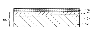
- FIG. 2 is a process cross-sectional view for explaining the method for manufacturing the nitride semiconductor device.
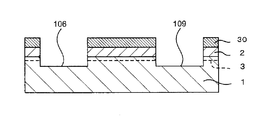
- FIG. 3 is a process cross-sectional view subsequent to FIG.
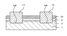
- FIG. 4 is a process cross-sectional view subsequent to FIG.
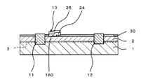
- FIG. 5 is a process cross-sectional view subsequent to FIG.
- FIG. 6 is a process cross-sectional view subsequent to FIG.
- FIG. 7 is a process cross-sectional view subsequent to FIG.
- FIG. 8 is a view showing a scanning electron microscope image showing a cross-sectional structure of the gate electrode of the nitride semiconductor device.
- FIG. 9 is a diagram showing a line analysis result of the scanning electron microscope image shown in FIG.
- FIG. 10 is a view showing a scanning electron microscope image showing a cross-sectional structure of a gate electrode of a nitride semiconductor device as a comparative example.
- FIG. 11 is a diagram showing a line analysis result of the scanning electron microscope image shown in FIG.
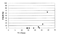
- FIG. 12 is a diagram showing the relationship between the average size in the thickness direction of the column portion of the fine columnar structure of the first metal layer of the nitride semiconductor device and the gate leakage current failure rate.
- FIG. 13 is a diagram showing the relationship between the average size in the thickness direction of the column portion of the fine columnar structure of the second metal layer of the nitride semiconductor device and the gate leakage current failure rate.
- FIG. 10 is a view showing a scanning electron microscope image showing a cross-sectional structure of a gate electrode of a nitride semiconductor device as a comparative example.
- FIG. 11 is a
- FIG. 14 is a view showing a scanning electron microscope image showing a cross-sectional structure of the gate electrode of the nitride semiconductor device according to the second embodiment of the present invention.
- FIG. 15 is a diagram showing the relationship between the average size in the thickness direction of the column portion of the fine columnar structure of the second metal layer of the nitride semiconductor device and the gate leakage current failure rate.
- FIG. 1 shows a cross-sectional view of a GaN-based HFET (Hetero-junction Field Effect Transistor) according to a first embodiment of the present invention.
- GaN-based HFET Hetero-junction Field Effect Transistor
- the nitride semiconductor device includes a Si substrate 10, an undoped AlGaN buffer layer 15 formed on the Si substrate 10, and a nitride semiconductor stacked layer formed on the undoped AlGaN buffer layer 15. And a body 20.
- the nitride semiconductor stacked body 20 includes an undoped GaN layer 1 and an undoped AlGaN layer 2.
- a 2DEG layer (two-dimensional electron gas layer) 3 is generated near the interface between the undoped GaN layer 1 and the undoped AlGaN layer 2.
- the GaN layer 1 may be replaced with an AlGaN layer having a composition having a smaller band gap than the AlGaN layer 2. Further, a layer having a thickness of about 1 nm made of GaN, for example, may be provided on the AlGaN layer 2 as a cap layer.
- the nitride semiconductor layer 20 is formed of two semiconductor layers, but is not limited to this, and may be formed of three nitride semiconductor layers.
- the nitride semiconductor device includes a source electrode 11 and a drain electrode 12. Further, the source electrode 11 and the drain electrode 12 are formed on the AlGaN layer 2 with a space therebetween. The source electrode 11 and the drain electrode 12 are formed in recesses 106 and 109 that penetrate the AlGaN layer 2 and the 2DEG layer 3 and reach the GaN layer 1.
- a gate electrode 13 is formed on the AlGaN layer 2 and on the source electrode side between the source electrode 11 and the drain electrode 12.
- the source electrode 11 and the drain electrode 12 are ohmic electrodes, and the gate electrode 13 is a Schottky electrode.
- the source electrode 11, the drain electrode 12, the gate electrode 13, and the active region constitute an HFET.
- the gate electrode 13 is an example of a metal electrode layer.
- the active region is a region of the nitride semiconductor stacked body 20 (GaN layer 1, AlGaN layer 2) in which carriers flow between the source electrode 11 and the drain electrode 12 by a voltage applied to the gate electrode 13. It is.
- an insulating film 30 made of SiO 2 is formed on the AlGaN layer 2.
- An interlayer insulating film 40 made of polyimide is formed on the insulating film 30 so as to cover the source electrode 11, the drain electrode 12, and the gate electrode 13.
- vias 41 as contact portions are formed in regions on the source electrode 11, the drain electrode 12 and the gate electrode 13 (the vias on the source electrode 11 and the gate electrode 13 are not shown in FIG. 1). Respectively.
- the via 41 is filled with a part of the drain electrode pad 42 and connected to the drain electrode pad 42.
- the material of the insulating film 30 is not limited to SiO 2 but may be SiN or Al 2 O 3 .
- the insulating film 30 may have a multilayer structure of a SiN film whose stoichiometry is broken on the surface of the semiconductor layer to suppress current collapse and a SiO 2 film or SiN film for surface protection.
- the material of the interlayer insulating film 40 is not limited to polyimide, but is a SiO 2 film manufactured by p-CVD (plasma chemical vapor deposition), SOG (Spin On Glass: coated glass), BPSG (boron / phosphorus / silicate / It may be an insulating material such as glass.
- current collapse is a phenomenon in which the on-resistance of a transistor in a high-voltage operation becomes higher than the on-resistance of the transistor in a low-voltage operation.
- the channel layer is controlled by applying a voltage to the gate electrode 13, and the HFET having the source electrode 11, the drain electrode 12, and the gate electrode 13 is turned on / off.
- the HFET when a negative voltage is applied to the gate electrode 13, a depletion layer is formed in the GaN layer 1 below the gate electrode 13, and the HFET is turned off.
- the HFET 13 when the voltage of the gate electrode 13 is zero, the HFET 13 is a normally-on type transistor in which the depletion layer disappears in the lower GaN layer 1 and is turned on.
- the Si substrate 10 and the AlGaN buffer layer 15 are not shown in order to make the drawings easy to see, and the sizes and intervals of the gate electrode 13, the source electrode 11, and the drain electrode 12 are changed. .
- an AlGaN buffer layer 15, a GaN layer 101, and an AlGaN layer 102 are sequentially formed on the Si substrate 10 by using an MOCVD (Metal-Organic-Chemical-Vapor-Deposition) method.
- MOCVD Metal-Organic-Chemical-Vapor-Deposition
- the thickness of the GaN layer 101 is 1 ⁇ m, for example, and the thickness of the AlGaN layer 102 is 30 nm, for example.
- the GaN layer 101 and the AlGaN layer 102 constitute a nitride semiconductor stacked body 120.
- an insulating film 130 (for example, SiO 2 ) is formed on the AlGaN layer 102 to a thickness of 200 nm by, for example, a plasma CVD (Chemical Vapor Deposition) method.
- the 2DEG layer 103 is formed in the vicinity of the heterointerface between the GaN layer 101 and the AlGaN layer 102.
- a portion where an ohmic electrode is to be formed is removed by dry etching.
- recesses 106 and 109 deeper than the 2DEG layer 103 are formed from the upper surface of the insulating film 130 to a part of the upper side of the GaN layer 101.
- the depths of the recesses 106 and 109 may be equal to or greater than the depth from the surface of the AlGaN layer 102 to the 2DEG layer 103, for example, 50 nm.
- the self-bias potential Vdc of an RIE (reactive ion etching) apparatus is set to 180 V or more and 240 V or less.
- O 2 plasma treatment cleaning with HCl / H 2 O 2 and cleaning with BHF (buffered hydrofluoric acid) or 1% HF (hydrofluoric acid) are sequentially performed on the surfaces of the recesses 106 and 109 against.
- annealing is performed (for example, 500 to 850 ° C.) in order to reduce etching damage due to dry etching.
- Ti / Al / TiN is laminated on the insulating film 30 and the recesses 106 and 109 by sputtering to form a laminated metal film 107 to be an ohmic electrode.
- the TiN layer is a cap layer for protecting the Ti / Al layer from a subsequent process.
- a small amount for example, 5 sccm
- the flow rate of oxygen flowing into the chamber is set so that Ti oxide is not generated.
- the pattern of the source electrode 11 and the drain electrode 12 is formed by using normal photolithography and dry etching.
- An ohmic contact is obtained between the 2DEG layer 3 and the source electrode 11 and drain electrode 12 by annealing the substrate on which the source electrode 11 and drain 12 are formed, for example, at 400 ° C. or more and 500 ° C. or less for 10 minutes or more. It is done.
- a mask is formed on a photoresist (not shown) by photolithography, and then the gate electrode 13 of the insulating film 30 is formed between the source electrode 11 and the drain electrode 12 by etching. A region 160 to be formed is removed to form a recess 160.
- a gate metal film is formed on the photoresist and the concave portion 160 by sputtering with a film thickness ranging from 150 nm to 250 nm, and then the gate electrode 13 protruding on the insulating film 30 is formed by lift-off.
- the gate electrode 13 has a first metal layer 24 having a fine columnar structure including a plurality of pillars A (shown in FIG. 8) and a fine columnar structure including a plurality of pillars B (shown in FIG. 8).
- the second metal layer 25 is laminated on the first metal layer 24.
- the junction between the first metal layer 24 and the AlGaN layer 2 is a Schottky junction.
- W tungsten nitride is used as the first metal layer 24, and W is used as the second metal layer 25.
- the column parts A and B of the fine columnar structure of the first and second metal layers 24 and 25 extend in a direction substantially parallel to the layer thickness direction.
- the columnar portion A of the fine columnar structure of the first metal layer 24 has a lower end bonded to the upper surface of the AlGaN layer 2 and an upper end bonded to the temporary surface of the second metal layer 25.
- the column part B of the fine columnar structure of the second metal layer 25 has its lower end joined to the upper surface of the first metal layer 24.
- the gate electrode 13 may be any material as long as the junction between the first metal layer 24 and the AlGaN layer 2 is a Schottky junction.
- the first metal layer 24 may be made of Ti nitride
- a thin film such as a SiN film whose stoichiometry is broken may be formed between the first metal layer 24 and the AlGaN layer 2, and the first metal layer 24 and the AlGaN layer 2 may be bonded to each other through this thin film.
- an interlayer insulating film 40 is formed on the insulating film 30. Then, dry etching using a fluorine-based gas is performed on the region of the interlayer insulating film 40 on the gate electrode 13. Thereby, as shown in FIG. 7, the interlayer insulating film 40 in which the via 51 is formed is obtained. A part of the gate electrode pad 52 in the via 51 is connected to the gate electrode 13. Similarly, for the source electrode 11 and the drain electrode 12, vias 41 (source electrodes) are formed in regions on the source electrode 11 (shown in FIG. 1) and the drain electrode 12 (shown in FIG. 1) of the interlayer insulating film 40 by dry etching. 11 is not shown, but the via 41 on the drain electrode 12 is formed as shown in FIG. 1, and the via 41 is filled with an electrode pad material, thereby nitriding as shown in FIG. A semiconductor device is formed.
- the gate electrode 13 was fabricated by setting the film forming conditions of the W nitride film used for the first metal layer 24 of the gate electrode 13 and the W film used for the second metal layer 25 as follows.
- FIG. 8 shows an example of a cross-sectional structure of the gate electrode 13 manufactured by the above manufacturing method.
- Ar flow rate 45-110sccm N 2 flow rate: 135-180sccm Chamber pressure: 35-83 mTorr DC output: 1000-1600W Deposition temperature: 300 ° C (W film)
- the average size in the thickness direction of the column part A of the fine columnar structure of the W nitride film produced under the above conditions was 23.2 nm.
- the average size in the thickness direction of the column part B of the fine columnar structure of the W film was 34.4 nm.
- the gate leakage current in the off state when 0V was applied to the drain electrode 12, 0V to the source electrode 111, and -20V to the gate electrode 13 was 0.7 nA. .
- the defect rate when the defect was 2.0 nA or more was 0.6%.
- a GaN-based HFET having a gate electrode 1013 as shown in FIG. 10 was formed.
- a W nitride film having an average size in the thickness direction of the column portion C of the fine columnar structure is 24.0 nm is used as the first metal layer 1024, and the thickness direction of the column portion D of the fine columnar structure is used.
- a W film having an average size of 22.5 nm was used as the second metal layer 1025.
- the gate leakage current was 1.6 nA, and the gate leakage current failure rate was 93%.
- the substrate of the target nitride semiconductor device is cleaved so that the cross section of the gate electrode is exposed, and the cleaved portion is observed using a scanning electron microscope as shown in FIGS.
- FIGS. 9 and 11 A line analysis image of secondary electrons as shown in FIGS. 9 and 11 is obtained.
- the average of the half width of the convex portion of the line analysis image within the scanning range is determined as the target nitride.
- the average size in the thickness direction of the column portion of the fine columnar structure of the semiconductor device was used.
- FIG. 12 shows the relationship between the average size in the thickness direction of the column portion A of the fine columnar structure of the first metal layer 24 of the gate electrode 13 of the GaN-based HFET and the gate leakage current defect rate.
- FIG. 13 shows the relationship between the average size in the thickness direction of the column portion B of the fine columnar structure of the second metal layer 25 of the gate electrode 13 of the GaN-based HFET and the gate leakage current defect rate.
- the gate leakage current failure rate is less than 5%. This is considered to be because when the average size in the thickness direction of the columnar portion A exceeds 25 nm, the internal stress of the first metal layer 24 increases and the leakage at the interface with the AlGaN layer 2 increases. .
- the average size in the thickness direction of the column part A of the first metal layer 24 fine columnar structure is less than 5 nm, the columnar structure is no longer a fine columnar structure, and the internal stress with the second metal layer 25 increases. Thereby, the adhesiveness between the 1st metal layer 24 and the 2nd metal layer 25 falls, and the 2nd metal layer 25 becomes easy to raise
- the W nitride film used as the first metal layer 24 has a fine columnar structure when the DC output is reduced in the range of 1000 to 1600 W and the N 2 / Ar flow rate ratio is increased. There was a tendency that the average size of the column part A in the thickness direction was small. In particular, by reducing the total flow rate of N 2 and Ar, there was an effect in forming a fine columnar structure in which the average size in the thickness direction of the column A was small. In the pressure range of 35-83 mTorr in the chamber, lowering the total flow rate of N 2 and Ar and lowering the pressure in the chamber was effective in reducing the average size in the direction of the thickness of the fine columnar structure. This is presumably because the scattering of sputtered particles decreases and the growth rate of the columnar structure increases when the pressure in the chamber decreases.
- the gate leakage current failure rate is less than 1%.
- the average size in the thickness direction of the columnar portion B of the fine columnar structure of the second metal layer 25 is less than 30 nm, the average size in the thickness direction of the columnar portion B of the fine columnar structure of the second metal layer 25 is When the via 51 is formed, it becomes close to the average size in the thickness direction of the column part A of the fine columnar structure of the first metal layer 24 as the base, and the continuity of the structure (continuity of grain boundaries) is strengthened.
- the second metal layer 25 must have a fine columnar structure, and the average size in the thickness direction is preferably less than 150 nm.
- the average size in the thickness direction of the column part A of the fine columnar structure tends to increase as the DC output increases in the range of 1000 to 1600 W during the film formation. was there.
- lowering the Ar flow rate and lowering the pressure in the chamber had an effect in forming a fine columnar structure with high adhesion to the first metal layer 24. This is thought to be because the scattering of sputtered particles is reduced and the growth rate in the vertical direction of the columnar structure is increased by lowering the Ar flow rate and lowering the pressure in the chamber.
- the average size in the thickness direction of the column portion B of the fine columnar structure of the second metal layer 25 is larger than the average size in the thickness direction of the column portion A of the fine columnar structure of the first metal layer 24.
- the gate leakage current can be greatly reduced, and it has been found that the gate leakage current failure rate can be remarkably improved.
- the average size in the thickness direction of the column part A of the fine columnar structure of the first metal layer 24 is 25 nm or less
- the average size in the thickness direction of the column part B of the fine columnar structure of the second metal layer 25 is 30 nm or more. As a result, the gate leakage current failure rate could be further improved.
- the GaN-based HFET according to the second embodiment has basically the same configuration as the GaN-based HFET according to the first embodiment shown in FIG. 1, and has the same steps as the method for manufacturing the GaN-based HFET according to the first embodiment. Have. Therefore, the description of the configuration and the manufacturing method is omitted by using the description of FIGS. In the following description, the same reference numerals as those of the constituent parts of the first embodiment are attached to the same constituent parts as the welfare part of the GaN-based HFET of the first embodiment.
- the GaN-based HFET of the second embodiment is only provided with a second metal layer 225 (shown in FIG. 14) constituted by two layers of a W film and a Ti film instead of the second metal layer 25. Is different.
- the film forming conditions for the W nitride film used for the first metal layer 24 and the W film and Ti film used for the second metal layer 225 are set as follows.
- FIG. 14 is an example of a cross-sectional structure of the manufactured gate electrode 213.
- the average size in the thickness direction of the columnar portion A of the fine columnar structure of the W nitride film, the columnar portion F of the fine columnar structure of the W film, and the columnar portion G of the fine columnar structure of Ti nitride is 23.2 nm, 36 8 nm and 33.7 nm.
- the substrate 10 of the target nitride semiconductor device is cleaved so that the cross section of the gate electrode 213 is exposed, and the cleaved portion is observed using a scanning electron microscope as shown in FIG.
- a direction perpendicular to the length direction of the columnar portion A of the fine columnar structure of the first metal layer 24 and the columnar portions F and G of the fine columnar structure of the second metal layer 225 (perpendicular to the layer thickness direction). Scan the electron beam of the scanning electron microscope in the direction).
- the secondary electron line analysis images as shown in FIGS.
- FIG. 15 is a diagram showing the relationship between the average size in the thickness direction of the column portion FG of the fine columnar structure of the second metal layer 125 of the GaN-based HFET and the gate leakage current failure rate.
- the gate leakage current failure rate becomes 0%. This is because the continuity of the structure with the fine columnar structure of the first metal layer 24 is further reduced by making the fine columnar structure of the second metal layer 225 into a two-layer structure of a W film and Ti nitride, and the via 51 This is probably because the damage to the insulating film 130 due to plasma could be suppressed during the dry etching when forming the film.
- the gate leakage current defect rate is further improved as compared with the case where the second metal layer 25 including only the W film is used. I understood it.
- the average size in the thickness direction of the column portions F and G of the fine columnar structure of the second metal layer 225 is the same as the thickness direction of the column portion A of the fine columnar structure of the first metal layer 24. “To be larger than the average size” means that the average size in the thickness direction of the columnar portions F and G of the two fine columnar structures of the second metal layer 225 is the thickness of the columnar A of the first metal layer. This means that it is larger than the average size in the direction (that is, A ⁇ F and A ⁇ G).
- the GaN-based HFET includes the Si substrate.
- the GaN-based HFET is not limited to the Si substrate, and may include a sapphire substrate or a SiC substrate.
- a nitride semiconductor layer may be grown on the sapphire substrate or the SiC substrate.
- a nitride semiconductor layer may be grown on a substrate made of a nitride semiconductor, such as growing an AlGaN layer on a GaN substrate.
- a buffer layer may be formed between the substrate and the nitride semiconductor layer, or the hetero-improvement may be provided between the first nitride semiconductor layer and the second nitride semiconductor layer of the nitride semiconductor stacked body.
- a layer may be formed.
- the GaN-based HFET has a recess structure.
- the present invention is not limited to this, and the GaN-based HFET does not have a recess structure, and a source electrode and a drain electrode are formed on the AlGaN layer. You may make it do.
- the GaN-based HFET configured to form the 2DEG layer is used as the nitride semiconductor device.
- the present invention is not limited to this, and other configurations are provided as the nitride semiconductor device.
- a field effect transistor may be used.
- a normally-on type GaN-based HFET is used as the nitride semiconductor device.
- the present invention is not limited thereto, and a normally-off type GaN-based HFET is used as the nitride semiconductor device. It may be used.
- a gate electrode having a Schottky junction is used as the electrode metal layer.
- the present invention is not limited to this, and a field effect transistor having an electrode insulated gate structure may be used as the electrode metal layer. .
- the nitride semiconductor of the nitride semiconductor device of the present invention only needs to be represented by Al x In y Ga 1-xy N (x ⁇ 0, y ⁇ 0, 0 ⁇ x + y ⁇ 1).
- the nitride semiconductor device of the present invention is not limited to an HFET that uses 2DEG, but is also a field effect of other configurations such as a MIS (Metal Insulator Semiconductor) FET, a MOS (Metal Oxide Semiconductor) FET, and a MES (Metal Semiconductor) FET. Even if it is a transistor, the same effect is acquired.
- MIS Metal Insulator Semiconductor
- MOS Metal Oxide Semiconductor
- MES Metal Semiconductor
- the nitride semiconductor device of the present invention is A substrate 10; A nitride semiconductor stacked body 20 formed on the substrate 10 and having a heterointerface; Formed on the nitride semiconductor multilayer body 20, and comprising an electrode metal layer,
- the electrode metal layer is A first metal layer 24 bonded to the nitride semiconductor stacked body 20 and having a fine columnar structure including a plurality of column portions A;
- a second metal layer 25 that is laminated on the first metal layer 24 and has a fine columnar structure including a plurality of pillar portions B;
- the average size in the thickness direction of the column portion B of the second metal layer 25 is larger than the average size in the thickness direction of the column portion A of the first metal layer 24.
- the electrode metal layer when the gate electrode 13 is formed of the metal layer, the electrode metal layer has a fine columnar structure including a plurality of column portions A and is bonded to the nitride semiconductor stacked body 20. And a second metal layer 25 having a fine columnar structure including a plurality of pillar portions B and laminated on the first metal layer 24, and an average size in the thickness direction of the pillar portion B of the second metal layer 25
- the gate leakage current can be reduced.
- the fine columnar structure of the first metal layer 24 is made of tungsten nitride, and the average size in the thickness direction of the column portion A of the first metal layer 24 is 5 nm or more and 25 nm or less.
- the gate leak is reduced by setting the average size in the thickness direction of the column part A of the fine columnar structure of the first metal layer 24 to 25 nm or less.
- the current can be reduced.
- the average size in the thickness direction of the column part B of the second metal layer 25 is not less than 30 nm and not more than 150 nm.
- the gate leak is increased by setting the average size in the thickness direction of the column part B of the fine columnar structure of the second metal layer 25 to 30 nm or more.
- the current can be reduced.
- the second metal layer 25 is made of tungsten.
- the second metal layer 25 is made of tungsten, when the first metal layer 24 is tungsten nitride, the thickness direction of the column part B of the fine columnar structure of the second metal layer 25 is Even if the average size of the first metal layer 24 is different from the average size in the thickness direction of the column part A of the fine columnar structure of the first metal layer 24, high adhesion between the first metal layer 24 and the second metal layer 25 is achieved. As a result, it is possible to suppress a decrease in yield due to the occurrence of a gate leak defect while preventing film peeling.
- the second metal layer 225 includes a tungsten layer and a titanium nitride layer.
- the second metal layer 225 when the gate electrode 13 is formed of the electrode metal layer, the second metal layer 225 includes the tungsten layer and the titanium nitride layer so that the second metal layer 225 becomes the tungsten layer. Compared with the case of only comprising, the gate leakage current can be greatly reduced.
Landscapes
- Junction Field-Effect Transistors (AREA)
- Electrodes Of Semiconductors (AREA)
Abstract
Description
基板と、
上記基板上に形成され、ヘテロ界面を有する窒化物半導体積層体と、
上記窒化物半導体積層体上に形成され、電極金属層と
を備え、
上記電極金属層は、
上記窒化半導体積層体に接合すると共に、複数の柱部を含む微細柱状構造を有する第1金属層と、
上記第1金属層上に積層されると共に、複数の柱部を含む微細柱状構造を有する第2金属層と
を含み、
上記第2金属層の上記柱部の太さ方向の平均サイズが、上記第1金属層の上記柱部の太さ方向の平均サイズよりも大きいことを特徴とする。
上記第1金属層の上記微細柱状構造は、タングステン窒化物で構成され、上記第1金属の上記柱部の太さ方向の平均サイズが5nm以上25nm以下である。
上記第2金属層の上記柱部の太さ方向の平均サイズが30nm以上150nm以下である。
上記第2金属層は、タングステンで構成される。
上記第2金属層は、タングステン層とチタン窒化物層とで構成される。
図1は、本発明の第1実施形態のGaN系HFET(Hetero-junction Field Effect Transistor:ヘテロ接合電界効果トランジスタ)の断面図を示している。
(W窒化物膜)
Ar流量:45-110sccm
N2流量:135-180sccm
チャンバー内圧力:35-83mTorr
DC出力:1000-1600W
成膜温度:300℃
(W膜)
Ar流量:45-80sccm
チャンバー内圧力:4-10mTorr
DC出力:1000-1600W
成膜温度:300℃
次に、本発明の第2実施形態のGaN系HFETについて説明する。この第2実施形態のGaN系HFETは、基本的に、図1に示す第1実施形態のGaN系HFETと同様の構成であり、第1実施形態のGaN系HFETの製造方法と同様の工程を有する。そのため、図1~図7の説明を援用して、構成および製造方法の説明については省略する。また、以下では、上記第1実施形態のGaN系HFETの厚生部と同一構成部には、上記第1実施形態の構成部の参照番号と同一の参照番号付して説明する。
(W窒化物膜)
Ar流量:45-110sccm
N2流量:135-180sccm
チャンバー内圧力:35-83mTorr
DC出力:1000-1600W
成膜温度:300℃
(W膜)
Ar流量:40-80sccm
チャンバー内圧力:4-10mTorr
DC出力:1000-1600W
成膜温度:300℃
(Ti膜)
Ar流量:25-30sccm
N2流量:100-120sccm
チャンバー内圧力:4-10mTorr
DC出力:4000-5000W
成膜温度:50℃
基板10と、
上記基板10上に形成され、ヘテロ界面を有する窒化物半導体積層体20と、
上記窒化物半導体積層体20上に形成され、電極金属層と
を備え、
上記電極金属層は、
上記窒化半導体積層体20に接合すると共に、複数の柱部Aを含む微細柱状構造を有する第1金属層24と、
上記第1金属層24上に積層されると共に、複数の柱部Bを含む微細柱状構造を有する第2金属層25と
を含み、
上記第2金属層25の上記柱部Bの太さ方向の平均サイズが、上記第1金属層24の上記柱部Aの太さ方向の平均サイズよりも大きいことを特徴とする。
上記第1金属層24の上記微細柱状構造は、タングステン窒化物で構成され、上記第1金属層24の上記柱部Aの太さ方向の平均サイズが5nm以上25nm以下である。
上記第2金属層25の上記柱部Bの太さ方向の平均サイズが30nm以上150nm以下である。
上記第2金属層25は、タングステンで構成される。
上記第2金属層225は、タングステン層とチタン窒化物層とで構成される。
2,102 AlGaN層
3,103 2DEG層
10 Si基板
11 ソース電極
12 ドレイン電極
13,213 ゲート電極
15 AlGaNバッファ層
20,120 窒化物半導体積層体
24 第1の金属層
25,225 第2の金属層
30,130 絶縁膜
40,140 層間絶縁膜
41,51 ビア
42 ドレイン電極パッド
50 コンタクト部
52 ゲート電極パッド
106,109,160 凹部
A,B 柱部
Claims (5)
- 基板(10)と、
上記基板(10)上に形成され、ヘテロ界面を有する窒化物半導体積層体(1,2)と、
上記窒化物半導体積層体(1,2)上に形成された電極金属層(13)と
を備え、
上記電極金属層(13)は、
上記窒化半導体積層体(1,2)に接合すると共に、複数の柱部(A)を含む微細柱状構造を有する第1金属層(24)と、
上記第1金属層(24)上に積層されると共に、複数の柱部(B)を含む微細柱状構造を有する第2金属層(25)と
を含み、
上記第2金属層(25)の上記柱部(B)の太さ方向の平均サイズが、上記第1金属層(24)の上記柱部(A)の太さ方向の平均サイズよりも大きいことを特徴とする窒化物半導体装置。 - 請求項1に記載の窒化半導体装置において、
上記第1金属層(24)の上記微細柱状構造は、タングステン窒化物で構成され、上記第1金属層(24)の上記柱部(A)の太さ方向の平均サイズが、5nm以上25nm以下であることを特徴とする窒化物半導体装置。 - 請求項1または2に記載の窒化半導体装置において、
上記第2金属層(25)の上記柱部(B)の太さ方向の平均サイズが、30nm以上150nm以下であることを特徴とする窒化物半導体装置。 - 請求項1から3のいずれか1つに記載の窒化半導体装置において、
上記第2金属層(25)は、タングステンで構成されることを特徴とする窒化物半導体装置。 - 請求項1から3のいずれか1つに記載の窒化半導体装置において、
上記第2金属層(25)は、タングステン層とチタン窒化物層とで構成されることを特徴とする窒化物半導体装置。
Priority Applications (3)
| Application Number | Priority Date | Filing Date | Title |
|---|---|---|---|
| US14/772,283 US20160013276A1 (en) | 2013-04-12 | 2014-01-27 | Nitride semiconductor device |
| CN201480019229.8A CN105074888A (zh) | 2013-04-12 | 2014-01-27 | 氮化物半导体器件 |
| JP2015511121A JPWO2014167876A1 (ja) | 2013-04-12 | 2014-01-27 | 窒化物半導体装置 |
Applications Claiming Priority (2)
| Application Number | Priority Date | Filing Date | Title |
|---|---|---|---|
| JP2013-083892 | 2013-04-12 | ||
| JP2013083892 | 2013-04-12 |
Publications (1)
| Publication Number | Publication Date |
|---|---|
| WO2014167876A1 true WO2014167876A1 (ja) | 2014-10-16 |
Family
ID=51689294
Family Applications (1)
| Application Number | Title | Priority Date | Filing Date |
|---|---|---|---|
| PCT/JP2014/051694 Ceased WO2014167876A1 (ja) | 2013-04-12 | 2014-01-27 | 窒化物半導体装置 |
Country Status (4)
| Country | Link |
|---|---|
| US (1) | US20160013276A1 (ja) |
| JP (1) | JPWO2014167876A1 (ja) |
| CN (1) | CN105074888A (ja) |
| WO (1) | WO2014167876A1 (ja) |
Families Citing this family (3)
| Publication number | Priority date | Publication date | Assignee | Title |
|---|---|---|---|---|
| US9760837B1 (en) * | 2016-03-13 | 2017-09-12 | Microsoft Technology Licensing, Llc | Depth from time-of-flight using machine learning |
| CN112242441A (zh) * | 2019-07-16 | 2021-01-19 | 联华电子股份有限公司 | 高电子迁移率晶体管 |
| US12112983B2 (en) | 2020-08-26 | 2024-10-08 | Macom Technology Solutions Holdings, Inc. | Atomic layer deposition of barrier metal layer for electrode of gallium nitride material device |
Citations (4)
| Publication number | Priority date | Publication date | Assignee | Title |
|---|---|---|---|---|
| JP2006196764A (ja) * | 2005-01-14 | 2006-07-27 | Fujitsu Ltd | 化合物半導体装置 |
| JP2006237393A (ja) * | 2005-02-25 | 2006-09-07 | Rohm Co Ltd | 半導体装置およびその製造方法 |
| JP2008130874A (ja) * | 2006-11-22 | 2008-06-05 | Nissan Motor Co Ltd | 電極膜/炭化珪素構造体、炭化珪素ショットキバリアダイオード、金属−炭化珪素半導体構造電界効果トランジスタ、電極膜の成膜最適化方法および電極膜/炭化珪素構造体の製造方法 |
| JP2011176015A (ja) * | 2010-02-23 | 2011-09-08 | Denso Corp | ショットキーバリアダイオードを備えた炭化珪素半導体装置およびその製造方法 |
Family Cites Families (24)
| Publication number | Priority date | Publication date | Assignee | Title |
|---|---|---|---|---|
| JPS62112373A (ja) * | 1985-11-12 | 1987-05-23 | Seiko Instr & Electronics Ltd | Misトランジスタ−の製造方法 |
| US4913929A (en) * | 1987-04-21 | 1990-04-03 | The Board Of Trustees Of The Leland Stanford Junior University | Thermal/microwave remote plasma multiprocessing reactor and method of use |
| JPH0283920A (ja) * | 1988-09-20 | 1990-03-26 | Sharp Corp | 半導体装置の製造方法 |
| US6833161B2 (en) * | 2002-02-26 | 2004-12-21 | Applied Materials, Inc. | Cyclical deposition of tungsten nitride for metal oxide gate electrode |
| US6667525B2 (en) * | 2002-03-04 | 2003-12-23 | Samsung Electronics Co., Ltd. | Semiconductor device having hetero grain stack gate |
| KR100476926B1 (ko) * | 2002-07-02 | 2005-03-17 | 삼성전자주식회사 | 반도체 소자의 듀얼 게이트 형성방법 |
| US7122408B2 (en) * | 2003-06-16 | 2006-10-17 | Micron Technology, Inc. | Photodiode with ultra-shallow junction for high quantum efficiency CMOS image sensor and method of formation |
| JP4841844B2 (ja) * | 2005-01-05 | 2011-12-21 | 三菱電機株式会社 | 半導体素子 |
| JP4205119B2 (ja) * | 2006-06-27 | 2009-01-07 | シャープ株式会社 | ヘテロ接合電界効果型トランジスタおよびヘテロ接合電界効果型トランジスタの製造方法 |
| JP2008108870A (ja) * | 2006-10-25 | 2008-05-08 | Sharp Corp | 整流器 |
| JP4296195B2 (ja) * | 2006-11-15 | 2009-07-15 | シャープ株式会社 | 電界効果トランジスタ |
| US7973304B2 (en) * | 2007-02-06 | 2011-07-05 | International Rectifier Corporation | III-nitride semiconductor device |
| US8035130B2 (en) * | 2007-03-26 | 2011-10-11 | Mitsubishi Electric Corporation | Nitride semiconductor heterojunction field effect transistor having wide band gap barrier layer that includes high concentration impurity region |
| JP5324076B2 (ja) * | 2007-11-21 | 2013-10-23 | シャープ株式会社 | 窒化物半導体用ショットキー電極および窒化物半導体装置 |
| JP2009152353A (ja) * | 2007-12-20 | 2009-07-09 | Mitsubishi Electric Corp | ヘテロ接合電界効果型トランジスタおよびその製造方法 |
| US7674707B2 (en) * | 2007-12-31 | 2010-03-09 | Texas Instruments Incorporated | Manufacturable reliable diffusion-barrier |
| JP5564791B2 (ja) * | 2008-12-26 | 2014-08-06 | 富士通株式会社 | 化合物半導体装置及びその製造方法 |
| JP4786730B2 (ja) * | 2009-05-28 | 2011-10-05 | シャープ株式会社 | 電界効果型トランジスタおよびその製造方法 |
| TW201110344A (en) * | 2009-09-04 | 2011-03-16 | Univ Nat Chiao Tung | GaN transistor with nitrogen-rich tungsten nitride Schottky gate contact and method of forming the same |
| JP2013076104A (ja) * | 2009-12-28 | 2013-04-25 | Canon Anelva Corp | マグネトロンスパッタリング装置及び電子部品の製造方法 |
| JP5575816B2 (ja) * | 2010-01-25 | 2014-08-20 | シャープ株式会社 | 複合型半導体装置 |
| KR20130004760A (ko) * | 2011-07-04 | 2013-01-14 | 삼성전자주식회사 | 파워소자 및 이의 제조방법 |
| JP5220904B2 (ja) * | 2011-08-05 | 2013-06-26 | シャープ株式会社 | GaN系化合物半導体装置 |
| TWI458092B (zh) * | 2012-01-10 | 2014-10-21 | 國立交通大學 | 具有高電子遷移率之氮化鎵電晶體結構 |
-
2014
- 2014-01-27 CN CN201480019229.8A patent/CN105074888A/zh active Pending
- 2014-01-27 JP JP2015511121A patent/JPWO2014167876A1/ja active Pending
- 2014-01-27 WO PCT/JP2014/051694 patent/WO2014167876A1/ja not_active Ceased
- 2014-01-27 US US14/772,283 patent/US20160013276A1/en not_active Abandoned
Patent Citations (4)
| Publication number | Priority date | Publication date | Assignee | Title |
|---|---|---|---|---|
| JP2006196764A (ja) * | 2005-01-14 | 2006-07-27 | Fujitsu Ltd | 化合物半導体装置 |
| JP2006237393A (ja) * | 2005-02-25 | 2006-09-07 | Rohm Co Ltd | 半導体装置およびその製造方法 |
| JP2008130874A (ja) * | 2006-11-22 | 2008-06-05 | Nissan Motor Co Ltd | 電極膜/炭化珪素構造体、炭化珪素ショットキバリアダイオード、金属−炭化珪素半導体構造電界効果トランジスタ、電極膜の成膜最適化方法および電極膜/炭化珪素構造体の製造方法 |
| JP2011176015A (ja) * | 2010-02-23 | 2011-09-08 | Denso Corp | ショットキーバリアダイオードを備えた炭化珪素半導体装置およびその製造方法 |
Also Published As
| Publication number | Publication date |
|---|---|
| CN105074888A (zh) | 2015-11-18 |
| JPWO2014167876A1 (ja) | 2017-02-16 |
| US20160013276A1 (en) | 2016-01-14 |
Similar Documents
| Publication | Publication Date | Title |
|---|---|---|
| US11296195B2 (en) | Semiconductor device manufacturing method | |
| JP5348364B2 (ja) | ヘテロ接合型電界効果半導体装置 | |
| TWI725433B (zh) | 半導體裝置的製作方法 | |
| JP5166576B2 (ja) | GaN系半導体素子の製造方法 | |
| JP2014045174A (ja) | 窒化物半導体装置 | |
| JP6240460B2 (ja) | 電界効果型化合物半導体装置及びその製造方法 | |
| US20160071939A1 (en) | Semiconductor device | |
| KR102261740B1 (ko) | 고주파 소자 및 이의 제조 방법 | |
| WO2014148255A1 (ja) | 窒化物半導体装置および窒化物半導体装置の製造方法 | |
| WO2012111363A1 (ja) | 横型半導体装置 | |
| CN103930978A (zh) | 场效应晶体管及其制造方法 | |
| WO2013153927A1 (ja) | 窒化物半導体装置 | |
| JP6530210B2 (ja) | 半導体装置及びその製造方法 | |
| TWI488303B (zh) | 增強型氮化鎵電晶體元件 | |
| WO2014167876A1 (ja) | 窒化物半導体装置 | |
| CN110875383B (zh) | 半导体装置及其制造方法 | |
| JP5750382B2 (ja) | 窒化物半導体装置 | |
| JP5917990B2 (ja) | 窒化物半導体装置 | |
| JP6255508B2 (ja) | 窒化物半導体装置 | |
| JP5220904B2 (ja) | GaN系化合物半導体装置 | |
| TWI740058B (zh) | 半導體裝置及其製造方法 | |
| WO2014129245A1 (ja) | 窒化物半導体装置 | |
| CN105789297A (zh) | 半导体装置 | |
| CN111987141A (zh) | 半导体装置及其制造方法 | |
| JP2013222800A (ja) | 窒化物半導体装置およびその製造方法 |
Legal Events
| Date | Code | Title | Description |
|---|---|---|---|
| WWE | Wipo information: entry into national phase |
Ref document number: 201480019229.8 Country of ref document: CN |
|
| 121 | Ep: the epo has been informed by wipo that ep was designated in this application |
Ref document number: 14783324 Country of ref document: EP Kind code of ref document: A1 |
|
| ENP | Entry into the national phase |
Ref document number: 2015511121 Country of ref document: JP Kind code of ref document: A |
|
| WWE | Wipo information: entry into national phase |
Ref document number: 14772283 Country of ref document: US |
|
| NENP | Non-entry into the national phase |
Ref country code: DE |
|
| 122 | Ep: pct application non-entry in european phase |
Ref document number: 14783324 Country of ref document: EP Kind code of ref document: A1 |