WO2014148133A1 - 積層セラミックコンデンサ - Google Patents
積層セラミックコンデンサ Download PDFInfo
- Publication number
- WO2014148133A1 WO2014148133A1 PCT/JP2014/052674 JP2014052674W WO2014148133A1 WO 2014148133 A1 WO2014148133 A1 WO 2014148133A1 JP 2014052674 W JP2014052674 W JP 2014052674W WO 2014148133 A1 WO2014148133 A1 WO 2014148133A1
- Authority
- WO
- WIPO (PCT)
- Prior art keywords
- outer layer
- layer
- ceramic
- ceramic capacitor
- multilayer ceramic
- Prior art date
- Legal status (The legal status is an assumption and is not a legal conclusion. Google has not performed a legal analysis and makes no representation as to the accuracy of the status listed.)
- Ceased
Links
Images
Classifications
-
- H—ELECTRICITY
- H01—ELECTRIC ELEMENTS
- H01G—CAPACITORS; CAPACITORS, RECTIFIERS, DETECTORS, SWITCHING DEVICES, LIGHT-SENSITIVE OR TEMPERATURE-SENSITIVE DEVICES OF THE ELECTROLYTIC TYPE
- H01G4/00—Fixed capacitors; Processes of their manufacture
- H01G4/30—Stacked capacitors
-
- H—ELECTRICITY
- H01—ELECTRIC ELEMENTS
- H01G—CAPACITORS; CAPACITORS, RECTIFIERS, DETECTORS, SWITCHING DEVICES, LIGHT-SENSITIVE OR TEMPERATURE-SENSITIVE DEVICES OF THE ELECTROLYTIC TYPE
- H01G2/00—Details of capacitors not covered by a single one of groups H01G4/00-H01G11/00
- H01G2/24—Distinguishing marks, e.g. colour coding
-
- H—ELECTRICITY
- H01—ELECTRIC ELEMENTS
- H01G—CAPACITORS; CAPACITORS, RECTIFIERS, DETECTORS, SWITCHING DEVICES, LIGHT-SENSITIVE OR TEMPERATURE-SENSITIVE DEVICES OF THE ELECTROLYTIC TYPE
- H01G4/00—Fixed capacitors; Processes of their manufacture
- H01G4/002—Details
- H01G4/005—Electrodes
- H01G4/012—Form of non-self-supporting electrodes
-
- H—ELECTRICITY
- H01—ELECTRIC ELEMENTS
- H01G—CAPACITORS; CAPACITORS, RECTIFIERS, DETECTORS, SWITCHING DEVICES, LIGHT-SENSITIVE OR TEMPERATURE-SENSITIVE DEVICES OF THE ELECTROLYTIC TYPE
- H01G4/00—Fixed capacitors; Processes of their manufacture
- H01G4/002—Details
- H01G4/018—Dielectrics
- H01G4/06—Solid dielectrics
- H01G4/08—Inorganic dielectrics
- H01G4/12—Ceramic dielectrics
-
- H—ELECTRICITY
- H01—ELECTRIC ELEMENTS
- H01G—CAPACITORS; CAPACITORS, RECTIFIERS, DETECTORS, SWITCHING DEVICES, LIGHT-SENSITIVE OR TEMPERATURE-SENSITIVE DEVICES OF THE ELECTROLYTIC TYPE
- H01G4/00—Fixed capacitors; Processes of their manufacture
- H01G4/002—Details
- H01G4/018—Dielectrics
- H01G4/06—Solid dielectrics
- H01G4/08—Inorganic dielectrics
- H01G4/12—Ceramic dielectrics
- H01G4/1209—Ceramic dielectrics characterised by the ceramic dielectric material
-
- H—ELECTRICITY
- H01—ELECTRIC ELEMENTS
- H01G—CAPACITORS; CAPACITORS, RECTIFIERS, DETECTORS, SWITCHING DEVICES, LIGHT-SENSITIVE OR TEMPERATURE-SENSITIVE DEVICES OF THE ELECTROLYTIC TYPE
- H01G4/00—Fixed capacitors; Processes of their manufacture
- H01G4/002—Details
- H01G4/018—Dielectrics
- H01G4/06—Solid dielectrics
- H01G4/08—Inorganic dielectrics
- H01G4/12—Ceramic dielectrics
- H01G4/1209—Ceramic dielectrics characterised by the ceramic dielectric material
- H01G4/1218—Ceramic dielectrics characterised by the ceramic dielectric material based on titanium oxides or titanates
- H01G4/1227—Ceramic dielectrics characterised by the ceramic dielectric material based on titanium oxides or titanates based on alkaline earth titanates
-
- H—ELECTRICITY
- H01—ELECTRIC ELEMENTS
- H01G—CAPACITORS; CAPACITORS, RECTIFIERS, DETECTORS, SWITCHING DEVICES, LIGHT-SENSITIVE OR TEMPERATURE-SENSITIVE DEVICES OF THE ELECTROLYTIC TYPE
- H01G4/00—Fixed capacitors; Processes of their manufacture
- H01G4/002—Details
- H01G4/018—Dielectrics
- H01G4/06—Solid dielectrics
- H01G4/08—Inorganic dielectrics
- H01G4/12—Ceramic dielectrics
- H01G4/1209—Ceramic dielectrics characterised by the ceramic dielectric material
- H01G4/1236—Ceramic dielectrics characterised by the ceramic dielectric material based on zirconium oxides or zirconates
-
- H—ELECTRICITY
- H01—ELECTRIC ELEMENTS
- H01G—CAPACITORS; CAPACITORS, RECTIFIERS, DETECTORS, SWITCHING DEVICES, LIGHT-SENSITIVE OR TEMPERATURE-SENSITIVE DEVICES OF THE ELECTROLYTIC TYPE
- H01G4/00—Fixed capacitors; Processes of their manufacture
- H01G4/002—Details
- H01G4/018—Dielectrics
- H01G4/06—Solid dielectrics
- H01G4/08—Inorganic dielectrics
- H01G4/12—Ceramic dielectrics
- H01G4/1209—Ceramic dielectrics characterised by the ceramic dielectric material
- H01G4/1236—Ceramic dielectrics characterised by the ceramic dielectric material based on zirconium oxides or zirconates
- H01G4/1245—Ceramic dielectrics characterised by the ceramic dielectric material based on zirconium oxides or zirconates containing also titanates
-
- H—ELECTRICITY
- H01—ELECTRIC ELEMENTS
- H01G—CAPACITORS; CAPACITORS, RECTIFIERS, DETECTORS, SWITCHING DEVICES, LIGHT-SENSITIVE OR TEMPERATURE-SENSITIVE DEVICES OF THE ELECTROLYTIC TYPE
- H01G4/00—Fixed capacitors; Processes of their manufacture
- H01G4/002—Details
- H01G4/224—Housing; Encapsulation
-
- H—ELECTRICITY
- H01—ELECTRIC ELEMENTS
- H01G—CAPACITORS; CAPACITORS, RECTIFIERS, DETECTORS, SWITCHING DEVICES, LIGHT-SENSITIVE OR TEMPERATURE-SENSITIVE DEVICES OF THE ELECTROLYTIC TYPE
- H01G4/00—Fixed capacitors; Processes of their manufacture
- H01G4/002—Details
- H01G4/228—Terminals
- H01G4/232—Terminals electrically connecting two or more layers of a stacked or rolled capacitor
-
- H—ELECTRICITY
- H01—ELECTRIC ELEMENTS
- H01G—CAPACITORS; CAPACITORS, RECTIFIERS, DETECTORS, SWITCHING DEVICES, LIGHT-SENSITIVE OR TEMPERATURE-SENSITIVE DEVICES OF THE ELECTROLYTIC TYPE
- H01G4/00—Fixed capacitors; Processes of their manufacture
- H01G4/002—Details
- H01G4/228—Terminals
- H01G4/242—Terminals the capacitive element surrounding the terminal
-
- H—ELECTRICITY
- H01—ELECTRIC ELEMENTS
- H01G—CAPACITORS; CAPACITORS, RECTIFIERS, DETECTORS, SWITCHING DEVICES, LIGHT-SENSITIVE OR TEMPERATURE-SENSITIVE DEVICES OF THE ELECTROLYTIC TYPE
- H01G4/00—Fixed capacitors; Processes of their manufacture
- H01G4/002—Details
- H01G4/228—Terminals
- H01G4/248—Terminals the terminals embracing or surrounding the capacitive element, e.g. caps
-
- H—ELECTRICITY
- H05—ELECTRIC TECHNIQUES NOT OTHERWISE PROVIDED FOR
- H05K—PRINTED CIRCUITS; CASINGS OR CONSTRUCTIONAL DETAILS OF ELECTRIC APPARATUS; MANUFACTURE OF ASSEMBLAGES OF ELECTRICAL COMPONENTS
- H05K1/00—Printed circuits
- H05K1/18—Printed circuits structurally associated with non-printed electric components
- H05K1/181—Printed circuits structurally associated with non-printed electric components associated with surface mounted components
-
- H—ELECTRICITY
- H05—ELECTRIC TECHNIQUES NOT OTHERWISE PROVIDED FOR
- H05K—PRINTED CIRCUITS; CASINGS OR CONSTRUCTIONAL DETAILS OF ELECTRIC APPARATUS; MANUFACTURE OF ASSEMBLAGES OF ELECTRICAL COMPONENTS
- H05K3/00—Apparatus or processes for manufacturing printed circuits
- H05K3/30—Assembling printed circuits with electric components, e.g. with resistors
-
- H—ELECTRICITY
- H05—ELECTRIC TECHNIQUES NOT OTHERWISE PROVIDED FOR
- H05K—PRINTED CIRCUITS; CASINGS OR CONSTRUCTIONAL DETAILS OF ELECTRIC APPARATUS; MANUFACTURE OF ASSEMBLAGES OF ELECTRICAL COMPONENTS
- H05K2201/00—Indexing scheme relating to printed circuits covered by H05K1/00
- H05K2201/10—Details of components or other objects attached to or integrated in a printed circuit board
- H05K2201/10007—Types of components
- H05K2201/10015—Non-printed capacitor
Definitions
- the present invention relates to a multilayer ceramic capacitor using a dielectric ceramic.
- a multilayer ceramic capacitor is composed of a rectangular parallelepiped laminate and external electrodes.
- the multilayer body includes a ceramic dielectric layer and internal electrodes that are arranged so as to face each other between the ceramic dielectric layers and are drawn to both ends of the multilayer body.
- the external electrodes are connected to the drawn internal electrodes at both ends of the laminate.
- This laminate includes an inner layer portion and an outer layer portion.
- the inner layer part is formed with a plurality of internal electrodes arranged to face each other.
- the outer layer portion is a portion between the two inner electrodes arranged on the outermost side among the plurality of inner electrodes and the side surface of the laminated body facing the inner electrode, that is, the outer portion of the inner layer portion of the laminated body.
- the outer layer portion and the inner layer portion are usually formed of the same material (for example, see Patent Document 1).
- this multilayer ceramic capacitor when this multilayer ceramic capacitor is mounted on a circuit board, the circuit board and the internal electrode are arranged in parallel, or the circuit board and the internal electrode are arranged orthogonally depending on the orientation of the multilayer ceramic capacitor. There is a case.
- the value of the generated stray capacitance varies depending on the positional relationship between the circuit board and the internal electrode, and the characteristics of the multilayer ceramic capacitor may be affected.
- the multilayer ceramic capacitor when mounting the multilayer ceramic capacitor on the circuit board, if the multilayer ceramic capacitor is packaged with the internal electrodes aligned in advance so that the positional relationship between the circuit board and the internal electrodes is the same, It can be mounted so that the positional relationship between the circuit board and the internal electrode is uniform, and the characteristic variation of the multilayer ceramic capacitor can be reduced.
- a main object of the present invention is to provide a multilayer ceramic capacitor that can indicate a mounting direction when the multilayer ceramic capacitor is mounted on a substrate.
- an inner layer portion in which a plurality of ceramic dielectric layers having internal electrodes are stacked and a plurality of ceramic dielectric layers in which no internal electrodes are formed are stacked outside the inner layer portion.
- the multilayer ceramic capacitor has at least a second outer layer mainly composed of an oxide different from the oxide of the first outer layer, a boundary reaction layer is disposed between the first outer layer and the second outer layer, and The reaction layer is adjacent to the first Among the elements constituting the oxide in the layer, at least one element other than oxygen, and among the elements constituting the oxide in the adjacent second outer layer, at least one element other than oxygen is included.
- the multilayer ceramic capacitor is characterized in that the color of the surface of the first outer layer is different from the color of the surface of the inner layer portion.
- the oxide in the second outer layer is preferably a perovskite type compound.
- the oxide in the first outer layer is preferably a perovskite compound.
- the color of the surface of the first outer layer and the color of the surface of the inner layer portion in the multilayer body are different. Therefore, the stacking direction of the internal electrodes can be confirmed from the appearance of the multilayer ceramic capacitor, and the multilayer ceramic capacitor can be mounted in consideration of the positional relationship between the substrate and the internal electrodes of the multilayer ceramic capacitor. According to the multilayer ceramic capacitor of the present invention, the characteristics of the multilayer ceramic capacitor can be improved if the oxide in the second outer layer or the first outer layer is a perovskite type compound.
- the surface direction of the internal electrode can be reliably grasped by the difference in the color of the side surface of the multilayer ceramic capacitor multilayer body. Therefore, when the multilayer ceramic capacitor is mounted on a substrate or the like, the multilayer ceramic capacitor can be mounted on the substrate in consideration of the positional relationship between the substrate and the internal electrodes in the multilayer body.
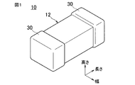
- FIG. 1 is an external perspective view showing an embodiment of a multilayer ceramic capacitor of the present invention.
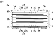
- FIG. 2 is an illustrative sectional view showing an internal structure of the multilayer ceramic capacitor shown in FIG. 1.
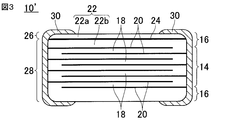
- FIG. 6 is a cross-sectional view showing another example of the internal structure of the multilayer ceramic capacitor shown in FIG. 1.
- FIG. 1 is an external perspective view showing an embodiment of a multilayer ceramic capacitor according to the present invention.
- FIG. 2 is an illustrative sectional view showing the internal structure of the multilayer ceramic capacitor shown in FIG.
- the multilayer ceramic capacitor 10 includes, for example, a rectangular parallelepiped multilayer body 12.
- the laminated body 12 is obtained by alternately laminating ceramic dielectric layers and internal electrodes, and the cross-sectional shape including the width direction and the height direction may be square or rectangular.
- the thickness of the ceramic dielectric layer constituting the laminated body 12 is about 0.5 to 5 ⁇ m, and the total number of laminated layers is 100 to 600.
- the laminated body 12 includes an inner layer portion 14 and an outer layer portion 16 as shown in FIG.
- the inner layer portion 14 has a configuration in which a plurality of ceramic dielectric layers 18 and internal electrodes 20 are alternately stacked. Adjacent internal electrodes 20 are formed to face each other with the ceramic dielectric layer 18 in between. The plurality of internal electrodes 20 are alternately drawn out to two opposing end surfaces of the multilayer body 12. That is, the adjacent internal electrodes 20 are drawn out to different end faces of the multilayer body 12, respectively.
- the internal electrode 20 is made of, for example, Ni or Cu, and is laminated with about 80 to 500 sheets.
- the inner layer portion 14 is a part of the laminated body 12 and is a range sandwiched between two internal electrodes 20 at both ends of the stacked internal electrodes 20.
- the outer layer portion 16 is composed of a plurality of ceramic dielectric layers 22 in which the internal electrode 20 is not formed, and is disposed so as to sandwich both sides of the inner layer portion 14.
- a boundary reaction layer 24 is formed in an intermediate portion of the outer layer portion 16. That is, the first outer layer 22 a is disposed outside the boundary reaction layer 24, and the second outer layer 22 b is disposed inside the boundary reaction layer 24. That is, the first outer layer 22a is located in the outermost layer.
- Each of the first outer layer 22a and the second outer layer 22b may be a single ceramic dielectric layer or a plurality of ceramic dielectric layers. Further, the thicknesses of the outer layer portions 16 sandwiching both sides of the inner layer portion 14 may be different. Further, another outer layer may be disposed between the second outer layer 22b and the inner layer portion 14.
- the first ceramic dielectric layer 26 is formed in a color different from that of the second ceramic dielectric layer 28, and is preferably formed in white.
- the first ceramic dielectric layer 26 coincides with the first outer layer 22 a disposed outside the boundary reaction layer 24 in the outer layer portion 16.
- the second ceramic dielectric layer 28 includes a ceramic dielectric layer 18 of the inner layer portion 14 and a second outer layer 22 b disposed inside the boundary reaction layer 24 of the outer layer portion 16.
- the boundary reaction layer 24 may be formed between the inner layer portion 14 and the outer layer portion 16. In this case, all the ceramic dielectric layers 22 constituting the outer layer portion 16 become the first ceramic dielectric layer 26, and all the ceramic dielectric layers 18 constituting the inner layer portion 14 become the second ceramic dielectric layer 28.
- the inner layer 14 and the outer layer part 16 can be firmly joined.
- the side surface of the multilayer body 12 (the side surface including the width direction and the length direction in FIG. 1) at the end in the stacking direction and the side surface (the height of FIG. It is possible to distinguish between the lateral direction including the longitudinal direction and the longitudinal direction. That is, the color of the first ceramic dielectric layer 26 can identify the side surfaces of the multilayer body 12 at both ends in the lamination direction.
- the main component of the ceramic dielectric layer 18 constituting the second ceramic dielectric layer 28 is a perovskite type compound represented by ABO 3 .
- A includes one or more of Ba, Sr, and Ca
- B includes one or more of Ti, Zr, and Hf
- O represents oxygen.
- the ceramic dielectric layer 18 constituting the inner layer portion 14 includes Dy, Mn, Mg, and Si as additive materials.
- the main components of the first outer layer 22a constituting the first ceramic dielectric layer 26 include an oxide containing Ca and Zr, and Si and Mn as additive materials.
- the main components of the second outer layer 22b constituting the second ceramic dielectric layer 28 include an oxide containing Ba and Ti and Si as an additive material.
- the oxide that is the main component of the first outer layer 22a and the second outer layer 22b is preferably a perovskite compound.
- the boundary reaction layer 24 formed between the first outer layer 22a and the second outer layer 22b includes at least one element other than oxygen among elements constituting the oxide in the first outer layer 22a, 2 Among the elements constituting the oxide in the outer layer 22b, at least one element other than oxygen is included.
- the composition has the above-described composition. be able to.
- the laminated body 12 is solidified and then polished to expose the cross sections cut in the thickness direction of the first outer layer 22a, the second outer layer 22b, and the boundary reaction layer 24, and composition analysis by WDX is also performed. It can be confirmed that it has the following composition.
- one or more elements other than oxygen constituting the main component of the second outer layer 22b may be diffused beyond the boundary reaction layer 24.
- the elements constituting the main component of the second outer layer 22b form the boundary reaction layer 24 near the interface between the second outer layer 22b and the boundary reaction layer 24 in the second outer layer 22b, as described above.
- a portion where the element concentration is thinner than the average concentration of the second outer layer 22b may be formed.
- External electrodes 30 are formed at both ends in the longitudinal direction of the laminate 12 so as to be connected to the drawn internal electrodes 20.
- the external electrode 30 is formed so as to go around the four side surfaces from the end surface of the multilayer body 12.
- the base metal layer is formed by immersing the edge part of the laminated body 12 in an electrode paste, and sintering.
- the external electrode 30 is formed by performing Ni plating and Sn plating on the base metal layer.
- the color of the first outer layer 22a and the color of the inner layer part 14 in the outer layer part 16 of the multilayer body 12 are different from each other. 20 can be confirmed, and the multilayer ceramic capacitor 10 can be mounted in consideration of the positional relationship between the substrate and the internal electrodes 20 of the multilayer ceramic capacitor.
- the oxides as the main components contained in the first outer layer 22a and the second outer layer 22b are different, but the first outer layer 22a.
- the first outer layer 22a and the second outer layer 22b can be firmly bonded.
- the oxide is different, except that the element constituting the oxide of the first outer layer 22a is at least one element different from the element constituting the oxide of the second outer layer 22b, except for trace elements such as impurities.
- a constituent element of the oxide of the second outer layer 22b includes at least one element different from the constituent element of the oxide of the first outer layer 22a. If the oxide that is the main component of the second outer layer 22b and the perovskite type compound that is the main component of the ceramic dielectric layer 18 constituting the inner layer portion 14 are the same type of compound, the second outer layer 22b and the inner layer portion 14 Can be firmly joined.
- the same species refers to compounds having the same constituent elements and crystal structures except for trace amounts of elements such as impurities, and the constituent element ratios may be different.
- FIG. 3 is an illustrative sectional view showing another embodiment of the internal structure of the multilayer ceramic capacitor 10 ′ according to the present invention.
- the multilayer ceramic capacitor 10 ′ has the first outer layer 22 a and the second outer layer 22 b formed only on one surface of the inner layer portion 14.
- the same ceramic dielectric layer as the ceramic dielectric layer 18 of the inner layer portion 14 is laminated to form an outer layer portion 16.
- the multilayer ceramic capacitor 10 ′ shown in FIG. 3 has the same effect as the multilayer ceramic capacitor 10 shown in FIG. In FIG. 2 and FIG. 3, the boundary reaction layer 24 is depicted as a single continuous layer, but may be a discontinuous layer.
- BaTiO 3 which is a ceramic raw material powder for forming the inner layer portion 14 is produced.
- BaCO 3 powder and TiO 2 powder are weighed so that the Ba / Ti ratio is 1.001 and wet-mixed by a mill using ZrO 2 balls.
- This mixed slurry is dried and then heated to 1000 ° C. to obtain BaTiO 3 powder having an average particle size of 0.16 ⁇ m.
- 1.0 mol part of Dy, 1.2 mol part of Mg, 0.2 mol part of Mn, and 1.0 mol part of Ba are added as a metal soap solution to 100 mol parts of this BaTiO 3 powder.
- 1.5 mol part of Si is added as alkoxide.
- the dispersion medium is mixed with a mixture of toluene and ethyl alcohol, and wet-mixed by a mill using ZrO 2 balls.
- the organic component is removed by heat treatment at 500 ° C., and the particle size is adjusted to obtain a ceramic raw material powder for forming the inner layer portion 14.
- a mixed dispersion medium of toluene and ethyl alcohol is added, and wet mixing is performed by a mill using ZrO 2 balls. And slurried. Next, this slurry is formed into a ceramic green sheet having a thickness of 1.0 ⁇ m by a gravure coater, and a ceramic green sheet for forming the inner layer portion 14 is prepared.
- the ceramic raw material powder for forming the first outer layer 22a and the ceramic raw material powder for forming the second outer layer 22b are each formed into a ceramic green sheet to form the first outer layer 22a.
- the ceramic green sheet and the ceramic green sheet for forming the second outer layer 22b are prepared.
- the ceramic raw material powder for forming the second outer layer 22b is the same as the ceramic raw material powder for forming the inner layer portion 14.
- the ceramic raw material powder for forming the first outer layer 22a is produced as follows. For example, first, CaCO 3 powder and ZrO 2 powder are weighed so that the Zr / Ti ratio is 1.000, and wet mixed by a mill using ZrO 2 balls. This mixed slurry is dried and then heated to 1100 ° C. to obtain a CaZrO 3 powder having an average particle size of 0.25 ⁇ m. Then, 1.0 mol part of MnCO 3 and 1.5 mol part of SiO 2 are added as powder to 100 mol parts of this CaZrO 3 powder. Subsequently, the dispersion medium is mixed with pure water by a mill using ZrO 2 balls. After drying, the ceramic raw material powder is sized to form the first outer layer 22a.
- a conductive paste for example, Ni paste
- a ceramic green sheet formed of a ceramic raw material powder for forming the inner layer portion 14 is screen-printed on a ceramic green sheet formed of a ceramic raw material powder for forming the inner layer portion 14 to form a conductive film pattern to be an internal electrode.
- the conductive film pattern is formed by, for example, screen printing or gravure printing.
- a plurality of ceramic green sheets on which the conductive film pattern is formed are laminated so that the conductive film pattern side is alternately arranged, and a portion corresponding to the inner layer portion 14 is obtained.
- a ceramic green sheet for forming the second outer layer 22b on which the conductive film pattern is not formed is laminated so as to sandwich the inner layer portion 14 therebetween. Further, a ceramic green sheet for forming the first outer layer 22a is laminated on the outside of the ceramic green sheet for forming the second outer layer 22b, and a portion corresponding to the outer layer portion 16 is formed. In this way, a mother laminate is produced.
- a ceramic green sheet for forming the first outer layer 22a to be the first ceramic dielectric layer 26 after firing, and the first outer layer 22b and the ceramic dielectric layer 18 to be the second ceramic dielectric layer 28 are formed.
- the ceramic green sheets are preferably formed by selecting dielectric materials having different colors after firing.
- the first ceramic dielectric layer 26 is made of a stable perovskite type compound such as CaZrO 3 having a valence of +2 for the A site element and +4 for the B site element.
- a perovskite type compound in which the valence of the A site element such as BaTiO 3 is +2 is stable and the valence of the B site element varies depending on the firing atmosphere is used.
- this mother laminated body was cut into a green laminated chip having a desired size. Then, the green laminate in an N 2 atmosphere, and heat treated at 270 ° C., the binder is burned and removed. Thereafter, the green laminated chip from which the binder was burned and removed was set at a temperature rising rate of 800 ° C. or higher at 30 ° C./min in a reducing atmosphere composed of N 2 —H 2 —H 2 O gas, and held at 1220 ° C.
- the laminated body 12 in which the boundary reaction layer 24 containing at least one element other than oxygen is formed is obtained.
- barrel polishing may be performed to round the corners of the green multilayer chip or the multilayer body 12.
- a base electrode is formed by applying a conductive paste containing Cu as a main component to both end portions of the laminate 12 from which the conductive film pattern to be the internal electrode 20 is drawn and baking it at a predetermined temperature.
- the external electrode 30 is formed on the base electrode by performing Ni—Sn plating, for example, by wet plating. In this way, a desired multilayer ceramic capacitor 10 is obtained.
- Example 1 Production of Ceramic Raw Material Powder for Forming Inner Layer Part Ceramic raw material powder for forming the inner layer part 14 was produced by the method described below. BaCO 3 powder and TiO 2 powder were weighed so that the Ba / Ti ratio was 1.001 and wet mixed by a mill using ZrO 2 balls. This mixed slurry was dried and then heated to 1000 ° C. to obtain BaTiO 3 powder having an average particle size of 0.16 ⁇ m. Then, 1.0 mol part of Dy, 1.2 mol part of Mg, 0.2 mol part of Mn, and 1.0 mol part of Ba are added as a metal soap solution to 100 mol parts of this BaTiO 3 powder. A further 1.5 mole parts of Si were added as alkoxide.
- the dispersion medium was wet mixed by a mill using ZrO 2 balls as a mixed system of toluene and ethyl alcohol. After removing the dispersion medium, the organic component was removed by heat treatment at 500 ° C., and the particle size was adjusted to produce a ceramic raw material powder for forming the inner layer portion 14.
- the ceramic raw material powder for forming the second outer layer 22b in the outer layer portion 16 is the same as the material used for preparing the ceramic raw material powder for forming the inner layer portion 14. The same material was used. Therefore, the main component of the ceramic raw material powder for forming the second outer layer 22b is BaTiO 3 .
- the ceramic raw material powder for forming the first outer layer 22a was produced as follows. First, the CaCO 3 powder and the ZrO 2 powder were weighed so that the Zr / Ti ratio was 1.000, and wet mixed by a mill using ZrO 2 balls. This mixed slurry was dried and then heated to 1100 ° C. to obtain CaZrO 3 powder having an average particle size of 0.25 ⁇ m. To 100 mol parts of this CaZrO 3 powder, 1.0 mol part of MnCO 3 and 1.5 mol part of SiO 2 are added as powders respectively, and wet-mixed by a mill using ZrO 2 balls as a dispersion medium as pure water. did. After drying, the ceramic raw material powder was sized to form the first outer layer 22a.
- a separately prepared Ni-containing conductive paste was screen-printed on a ceramic green sheet formed of ceramic raw material powder for forming the inner layer portion 14, thereby forming a conductive film pattern to be the internal electrode 14. Then, 400 sheets were laminated so that the conductive film pattern drawn side was alternated, and the inner layer part 14 was obtained.
- a ceramic green sheet formed of ceramic raw material powder for forming the second outer layer 22b is laminated so as to sandwich the inner layer portion 14 with a thickness of 48 ⁇ m, and the first outer layer 22a is formed on both outer sides thereof.
- the ceramic green sheets formed of the ceramic raw material powder for the purpose were laminated by 7 ⁇ m to prepare a mother laminate. This mother laminate was cut into green laminate chips having a desired size.
- the green multilayer chip thus fabricated was heat-treated at 270 ° C. in an N 2 atmosphere, and the binder was burned and removed. Thereafter, firing was carried out in a reducing atmosphere composed of N 2 —H 2 —H 2 O gas at a heating rate of 800 ° C. or higher at 30 ° C./min, at 1220 ° C. and a holding time of 5 minutes.
- the obtained laminate 12 had a size of 1.2 mm in length, 0.7 mm in width, 0.7 mm in height, and a prismatic shape with a square cross section.
- a conductive film paste containing Cu as a main component was applied to both end portions from which the conductive film pattern to be the internal electrode 20 was drawn, and baked at 800 ° C.
- the multilayer ceramic capacitor as shown in FIG. 2 was obtained. Note that the thickness of the element portion of the multilayer ceramic capacitor thus obtained was 0.85 ⁇ m.
- Example 2 In Example 2, after obtaining the inner layer portion 14 in the same manner as in Example 1, 48 ⁇ m of ceramic green sheets formed of ceramic raw material powder for forming the second outer layer 22b only on one side were laminated, A ceramic green sheet formed of ceramic raw material powder for forming the first outer layer 22a was laminated on the surface by 7 ⁇ m. On the other hand, on the other surface of the inner layer part 14, a ceramic green sheet formed of ceramic raw material powder for forming the inner layer part 14 was laminated by 55 ⁇ m to prepare a mother laminate. Then, by the same method as Example 1, it cut
- Example 3 In Example 3, unlike Example 1, the oxide that is the main component of the first outer layer 22a was SrZrO 3 .
- the SrCO 3 powder and the ZrO 2 powder are weighed so that the Sr / Zr ratio is 1.000. After mixing and pulverizing by a mill using ZrO 2 balls, the mixture was heated to 1050 ° C. to obtain SrZrO 3 powder.
- Example 2 After obtaining the inner layer part 14 by the method similar to Example 1, 48 micrometers of ceramic green sheets formed with the ceramic raw material powder for forming the 2nd outer layer 22b are laminated
- Example 4 In Example 4, unlike Example 1, the oxide that is the main component of the first outer layer 22a was (Ba 0.2 Sr 0.8 ) TiO 3 .
- first, SrCO 3 powder, BaCO 3 powder and TiO 2 powder are mixed and pulverized and heated to 1050 ° C., (Ba 0.2 Sr 0.8 ) TiO 3 powder.
- Example 2 After obtaining the inner layer part 14 by the method similar to Example 1, 48 micrometers of ceramic green sheets formed with the ceramic raw material powder for forming the 2nd outer layer 22b are laminated
- Comparative Example 1 In Comparative Example 1, unlike Example 1, BaTiO 3 which is the same ceramic raw material powder as the ceramic raw material powder for forming the inner layer portion 14 was used as the ceramic raw material powder for forming the outer layer portion 16. Then, in the same manner as in Example 1, it was cut into a green multilayer chip, fired, and the external electrode 30 was formed to produce a multilayer ceramic capacitor. Thus, a multilayer ceramic capacitor of Comparative Example 1 was obtained. .
- Comparative Example 2 In Comparative Example 2, unlike Example 1, the oxide as the main component of the first outer layer 22a was Ba (Ti 0.05 Zr 0.95 ) O 3 .
- the oxide as the main component of the first outer layer 22a was Ba (Ti 0.05 Zr 0.95 ) O 3 .
- BaCO 3 powder, TiO 2 powder and ZrO 2 powder are mixed and pulverized and heated to 1050 ° C.
- Ba (Ti 0.05 Zr 0.95 ) O 3 powder was obtained.
- 0.25 mol parts of MnCO 3 and 1.5 mol parts of SiO 2 are added as powders respectively, and ZrO 2 balls are added with pure water as a dispersion medium.
- Comparative Example 3 In Comparative Example 3, the same oxide as the main component of the first outer layer 22a as in Example 1 was CaZrO 3 , but the composition of the additive used in producing this was different. To 100 mol parts of the CaZrO 3 powder, 5.0 mol parts of MnCO 3 and 2.0 mol parts of SiO 2 are added as powders respectively, and wet-mixed by a mill using ZrO 2 balls with pure water as a dispersion medium. It was done. After drying, the particles were sized to produce a ceramic raw material powder for forming the first outer layer 22a used in Comparative Example 3.
- Example 2 After obtaining the inner layer part 14 by the method similar to Example 1, 48 micrometers of ceramic green sheets formed with the ceramic raw material powder for forming the 2nd outer layer 22b are laminated
- a cross section (LT cross section) in the height direction (T direction) and the length direction (L direction) in FIG. 1 of the multilayer ceramic capacitor 10 in each example and each comparative example is exposed by resin compaction and polishing, and the entire outer layer portion is scanned.
- Observation with a reflection electron image of a scanning electron microscope (SEM) and analysis of elemental analysis by wavelength dispersive X-ray spectroscopic analysis (WDX) confirmed whether or not a boundary reaction layer was formed.
- the polishing was performed to a depth of about 1 ⁇ 2 in the width direction.
- Table 1 shows the boundary for each case where the main component of the ceramic raw material powder for forming the first outer layer 22a and the main component of the ceramic raw material powder for forming the second outer layer 22b are used in each example and each comparative example. The presence or absence of the reaction layer 24, the possibility of outer layer identification, and the results of the bending strength test are shown.
- Example 1 to Example 4 it was confirmed from the reflected electron image that the boundary reaction layer 24 was formed in the outer layer part 16. Further, by wavelength dispersion X-ray spectroscopic analysis, at least one element other than oxygen among the elements constituting the main component of the first outer layer 22a and the main component of the second outer layer 22b are formed in the boundary reaction layer 24. It was confirmed that at least one element other than oxygen was included among the elements to be processed. In this analysis, when an element is detected by 0.1 wt% or more, it is assumed that the element is contained.
- Example 1 and Example 2 Ba and Ca are detected by 0.1 wt% or more from the boundary reaction layer 24, in Example 3, Ba and Sr are detected by 0.1 wt% or more, and in Example 4, Ba, Sr and Ti were detected by 0.1 wt% or more.
- the surface of the first outer layer 22a was white in Examples 1 to 3, and was slightly dull white in Example 4. Thereby, the surface of the side surface specified by the height direction and the length direction in FIG. 1 of the tea system could be identified. Furthermore, in Example 1 to Example 4, it was confirmed that the first outer layer 22a and the second outer layer 22b were firmly joined by forming the boundary reaction layer 24. Moreover, in Example 1 thru
- the first ceramic dielectric layer and the second ceramic dielectric layer used the ceramic raw material powder composed of the same main component, and thus the outer layer could not be identified.
- this invention is not limited to the said embodiment, In the range of the summary, it deform
Landscapes
- Engineering & Computer Science (AREA)
- Power Engineering (AREA)
- Microelectronics & Electronic Packaging (AREA)
- Manufacturing & Machinery (AREA)
- Chemical & Material Sciences (AREA)
- Ceramic Engineering (AREA)
- Inorganic Chemistry (AREA)
- Ceramic Capacitors (AREA)
- Fixed Capacitors And Capacitor Manufacturing Machines (AREA)
Abstract
積層セラミックコンデンサを基板上に実装する際に、実装方向を示すことができる積層セラミックコンデンサを提供する。 積層セラミックコンデンサ10は、セラミック誘電体層18と内部電極20とを有する内層部14と、セラミック誘電体層22からなる外層部16とを備えた積層体12を含む。積層体12の両端部に、内部電極20に接続された外部電極30が形成される。内層部14の主成分は、ABO3で表されるペロブスカイト型化合物である。外層部16は、それぞれ主成分が互いに異なる酸化物を含む第1外層22aおよび第2外層22bを含み、第1外層22aおよび第2外層22bの間に境界反応層24が形成される。そして、境界反応層24の外側の第1セラミック誘電体層26の色彩が、境界反応層24の内側の第2セラミック誘電体層28の色彩と異なるように形成される。
Description
この発明は、誘電体セラミックを用いた積層セラミックコンデンサに関する。
一般的に、積層セラミックコンデンサは、直方体状の積層体と外部電極とで構成される。積層体は、セラミック誘電体層と、セラミック誘電体層間で互いに対向するように配置され、積層体の両端部に引き出される内部電極とを有している。外部電極は、積層体の両端部において、引き出された内部電極に接続されている。この積層体は、内層部と外層部とを含む。内層部は、互いに対向するように配置された複数の内部電極が形成されている。外層部は、複数の内部電極のうち最も外側に配置された2つの内部電極とそれに対向する積層体の側面との間の部分、すなわち、積層体のうちの内層部の外側の部分である。この外層部と内層部とは、通常、同じ材料により形成されている(たとえば、特許文献1を参照)。
また、この積層セラミックコンデンサを回路基板上に実装する際に、積層セラミックコンデンサの向きによって、回路基板と内部電極とが平行に配置されたり、回路基板と内部電極とが直交するように配置されたりする場合がある。積層セラミックコンデンサは、このような回路基板と内部電極との位置関係により、発生する浮遊容量の値が変動し、積層セラミックコンデンサの特性に影響を与えてしまう場合がある。
したがって、積層セラミックコンデンサを回路基板上に実装する際に、回路基板と内部電極との位置関係が同じになるように、予め内部電極の方向を揃えて積層セラミックコンデンサをパッケージングしてあれば、回路基板と内部電極の位置関係が揃うように実装することができ、積層セラミックコンデンサの特性ばらつきを小さくすることができる。
しかしながら、内部電極は積層体内に埋設されているため、積層セラミックコンデンサの断面が正方形あるいは正方形に近い長方形である場合、積層セラミックコンデンサの外観から内部電極の積み重ね方向を見分けることは困難であるという問題があった。
それゆえに、この発明の主たる目的は、積層セラミックコンデンサを基板上に実装する際に、実装方向を示すことができる積層セラミックコンデンサを提供することである。
この発明にかかる積層セラミックコンデンサは、内部電極が形成された複数のセラミック誘電体層を積層した内層部と、内部電極が形成されていない複数のセラミック誘電体層を前記内層部の外側に積層した外層部とを備えた積層体、および積層体の両端部に形成される外部電極を含む積層セラミックコンデンサであって、内層部は、ABO3(ここでAはBa,Sr,Caの1種以上であり、BはTi,Zr,Hfの1種以上であり、Oは酸素)で表されるペロブスカイト型化合物を主成分とし、外層部は、酸化物を主成分とし、最外層である第1外層と、第1外層の酸化物とは異なる酸化物を主成分とする第2外層を少なくとも有しており、第1外層と第2外層間に境界反応層が配置されており、さらに、境界反応層には、隣接する第1外層中の酸化物を構成する元素のうち、酸素以外の少なくとも1つの元素と、隣接する第2外層中の酸化物を構成する元素のうち、酸素以外の少なくとも1つの元素と、が含まれており、第1外層の表面の色彩と内層部の表面の色彩とが異なることを特徴とする、積層セラミックコンデンサである。
また、この発明にかかる積層セラミックコンデンサは、第2外層中の前記酸化物がペロブスカイト型化合物であることが好ましい。
さらに、この発明にかかる積層セラミックコンデンサは、第1外層中の前記酸化物がペロブスカイト型化合物であることが好ましい。
また、この発明にかかる積層セラミックコンデンサは、第2外層中の前記酸化物がペロブスカイト型化合物であることが好ましい。
さらに、この発明にかかる積層セラミックコンデンサは、第1外層中の前記酸化物がペロブスカイト型化合物であることが好ましい。
この発明にかかる積層セラミックコンデンサによれば、積層体における第1外層の表面の色彩と内層部の表面の色彩とが異なっている。そのため、積層セラミックコンデンサの外観から内部電極の積層方向を確認することができ、基板と積層セラミックコンデンサの内部電極との位置関係を考慮して積層セラミックコンデンサを実装することができる。
また、この発明にかかる積層セラミックコンデンサによれば、第2外層中あるいは第1外層中の酸化物をペロブスカイト型化合物とすると、積層セラミックコンデンサの特性を向上させることができる。
また、この発明にかかる積層セラミックコンデンサによれば、第2外層中あるいは第1外層中の酸化物をペロブスカイト型化合物とすると、積層セラミックコンデンサの特性を向上させることができる。
この発明によれば、積層セラミックコンデンサの積層体の側面の色彩の違いによって、内部電極の面方向を確実に把握することができる。したがって、積層セラミックコンデンサを基板などに実装する際に、基板と積層体中の内部電極との位置関係を考慮して、積層セラミックコンデンサを基板上に実装することができる。
この発明の上述の目的、その他の目的、特徴および利点は、図面を参照して行う以下の発明を実施するための形態の説明から一層明らかとなろう。
(積層セラミックコンデンサの構造)
図1は、この発明にかかる積層セラミックコンデンサの一実施の形態を示す外観斜視図である。図2は、図1に示す積層セラミックコンデンサの内部構造を示す断面図解図である。
図1は、この発明にかかる積層セラミックコンデンサの一実施の形態を示す外観斜視図である。図2は、図1に示す積層セラミックコンデンサの内部構造を示す断面図解図である。
積層セラミックコンデンサ10は、たとえば直方体状の積層体12を含む。積層体12は、セラミック誘電体層と内部電極とを交互に積層したものであり、その幅方向と高さ方向とを含む断面形状は、正方形状であっても長方形状であってもよい。積層体12を構成するセラミック誘電体層の厚みは0.5~5μm程度であり、その総積層枚数は100~600枚である。
積層体12は、図2に示すように、内層部14と外層部16とを含む。
内層部14は、複数のセラミック誘電体層18と内部電極20とが交互に積層された構成を有する。隣接する内部電極20は、セラミック誘電体層18を挟んで互いに対向するように形成される。そして、複数の内部電極20は、積層体12の対向する2つの端面に交互に引き出される。つまり、隣接する内部電極20は、それぞれ積層体12の異なる端面に引き出される。内部電極20は、たとえばNiもしくはCuなどで形成され、80枚~500枚程度積層されている。内層部14は、積層体12の一部であり、積み重ねられた内部電極20のうちの両端の2つの内部電極20に挟まれた範囲のことである。
外層部16は、内部電極20が形成されていない複数のセラミック誘電体層22から構成されており、内層部14の両側を挟むように配置される。外層部16の中間部には、境界反応層24が形成される。つまり、境界反応層24の外側に第1外層22aが配置され、境界反応層24の内側に第2外層22bが配置されている。すなわち、第1外層22aは最外層に位置する。なお、第1外層22aおよび第2外層22bは、それぞれ1枚のセラミック誘電体層であってもよいし、複数枚のセラミック誘電体層であってもよい。また、内層部14の両側を挟むそれぞれの外層部16の厚みは異なっていてもよい。また、第2外層22bと内層部14間には、さらに他の外層が配置されていてもよい。
なお、第1セラミック誘電体層26は、第2セラミック誘電体層28と異なる色彩に形成されており、好ましくは、白色に形成される。ここで、第1セラミック誘電体層26は、外層部16のうちの境界反応層24の外側に配置された第1外層22aに一致する。また、第2セラミック誘電体層28は、内層部14のセラミック誘電体層18および外層部16のうちの境界反応層24の内側に配置された第2外層22bを含む。なお、境界反応層24は、内層部14と外層部16との間に形成されてもよい。この場合、外層部16を構成する全てのセラミック誘電体層22が第1セラミック誘電体層26となり、内層部14を構成する全てのセラミック誘電体層18が第2セラミック誘電体層28となる。それにより、内部層14と外層部16とを、強固に接合することができる。また、積層方向の端部にある積層体12の側面(図1の幅方向と長さ方向とを含む側面)と、第2セラミック誘電体層28の端部が露出する側面(図1の高さ方向と長さ方向とを含む側面)とを区別することができる。つまり、第1セラミック誘電体層26の色彩によって、積層方向の両端にある積層体12の側面であることを識別することができる。
第2セラミック誘電体層28を構成するセラミック誘電体層18の主成分は、ABO3で表されるペロブスカイト型化合物である。ここで、Aは、Ba,Sr,Caの1種以上を含み、Bは、Ti,Zr,Hfの1種以上を含み、Oは酸素を表す。さらに、内層部14を構成するセラミック誘電体層18は、Dy,Mn,Mg,Siを添加物素材として含む。
第1セラミック誘電体層26をサンドペーパー等で除去した後、残った第2セラミック誘電体層28を粉末状にし、酸によって溶解して、ICP発光分光分析を行った場合、上述のような組成を有していることを確認することができる。
第1セラミック誘電体層26をサンドペーパー等で除去した後、残った第2セラミック誘電体層28を粉末状にし、酸によって溶解して、ICP発光分光分析を行った場合、上述のような組成を有していることを確認することができる。
また、第1セラミック誘電体層26を構成する第1外層22aの主成分は、Ca,Zrを含む酸化物と、Si,Mnを添加物素材として含む。また、第2セラミック誘電体層28を構成する第2外層22bの主成分としては、Ba,Tiを含む酸化物と、Siを添加物素材として含む。また、第1外層22aおよび第2外層22bの主成分である酸化物は、ペロブスカイト型化合物であることが好ましい。
また、第1外層22aと第2外層22bとの間に形成される境界反応層24には、第1外層22a中の酸化物を構成する元素のうち、酸素以外の少なくとも1つの元素と、第2外層22b中の酸化物を構成する元素のうち、酸素以外の少なくとも1つの元素と、が含まれている。
このような主成分を有する第1外層22aおよび第2外層22bを粉末状にし、酸によって溶解して、ICP発光分光分析を行った場合、上述のような組成を有していることを確認することができる。
また、積層体12を樹脂固め後、研磨することによって第1外層22a、第2外層22bおよび境界反応層24の厚さ方向に切断した断面を露出させ、WDXによる組成分析を行うことでも、上述のような組成を有していることを確認することができる。
また、第1外層22aと第2外層22bとの間に形成される境界反応層24には、第1外層22a中の酸化物を構成する元素のうち、酸素以外の少なくとも1つの元素と、第2外層22b中の酸化物を構成する元素のうち、酸素以外の少なくとも1つの元素と、が含まれている。
このような主成分を有する第1外層22aおよび第2外層22bを粉末状にし、酸によって溶解して、ICP発光分光分析を行った場合、上述のような組成を有していることを確認することができる。
また、積層体12を樹脂固め後、研磨することによって第1外層22a、第2外層22bおよび境界反応層24の厚さ方向に切断した断面を露出させ、WDXによる組成分析を行うことでも、上述のような組成を有していることを確認することができる。
なお、第1外層22aには、第2外層22bの主成分を構成する酸素以外の1つ以上の元素が境界反応層24を超えて拡散している場合がある。
また、第2外層22b中の第2外層22bと境界反応層24との界面付近には、第2外層22bの主成分を構成する元素が境界反応層24を形成することに加え、上述したように、さらに、第1外層22a側へも拡散した結果、第2外層22bの平均濃度よりも前記元素濃度が薄くなった部分が形成される場合がある。
また、第2外層22b中の第2外層22bと境界反応層24との界面付近には、第2外層22bの主成分を構成する元素が境界反応層24を形成することに加え、上述したように、さらに、第1外層22a側へも拡散した結果、第2外層22bの平均濃度よりも前記元素濃度が薄くなった部分が形成される場合がある。
積層体12の長手方向の両端部には、引き出された内部電極20に接続されるようにして、外部電極30が形成される。外部電極30は、積層体12の端面から4つの側面に回り込むように形成される。外部電極30は、積層体12の端部を電極ペーストに浸漬し、焼結することによって下地金属層が形成される。この下地金属層上にNiめっきおよびSnめっきを施すことにより、外部電極30が形成される。
図2に示す積層セラミックコンデンサ10では、積層体12の外層部16における第1外層22aの色彩と内層部14の色彩とが異なることから、その色彩の違いによって、積層セラミックコンデンサの外観から内部電極20の積層方向を確認することができ、基板と積層セラミックコンデンサの内部電極20との位置関係を考慮して、積層セラミックコンデンサ10を実装することができる。
また、図2に示す積層セラミックコンデンサ10では、積層体12の外層部16において、第1外層22aと第2外層22bに含有される主成分である酸化物が異なっているが、第1外層22aと第2外層22bとの境界面に境界反応層24が形成されていることで、第1外層22aと第2外層22bとを、強固に接合することができる。ここで、酸化物が異なるとは、不純物程度の微量な元素を除き、第1外層22aの前記酸化物の構成元素が、第2外層22bの前記酸化物の構成元素とは異なる元素を少なくとも1種類以上含んでいる、あるいは、第2外層22bの前記酸化物の構成元素が、第1外層22aの前記酸化物の構成元素とは異なる元素を少なくとも1種類以上含んでいる状態を指す。
なお、第2外層22bの主成分である酸化物と内層部14を構成するセラミック誘電体層18の主成分であるペロブスカイト型化合物が同種の化合物であると、第2外層22bと内層部14とを強固に接合することができる。ここで、同種とは、不純物程度の微量な元素を除き、構成元素および結晶構造が同じ化合物を指し、構成元素比が異なっていてもよい。
なお、第2外層22bの主成分である酸化物と内層部14を構成するセラミック誘電体層18の主成分であるペロブスカイト型化合物が同種の化合物であると、第2外層22bと内層部14とを強固に接合することができる。ここで、同種とは、不純物程度の微量な元素を除き、構成元素および結晶構造が同じ化合物を指し、構成元素比が異なっていてもよい。
また、この発明にかかる積層セラミックコンデンサの他の実施の形態を示す。図3は、この発明にかかる積層セラミックコンデンサ10’の内部構造の他の実施の形態を示す断面図解図である。積層セラミックコンデンサ10’は、積層セラミックコンデンサ10とは異なり、内層部14の一方面のみ、第1外層22aおよび第2外層22bが形成されている。内層部14の他方面は、内層部14のセラミック誘電体層18と同一のセラミック誘電体層が積層され、外層部16が形成されている。
この図3に示す積層セラミックコンデンサ10’では、上述の図2に示す積層セラミックコンデンサ10と同様の効果を奏する。
なお、図2や図3において、境界反応層24は、連続した1枚の層として描かれているが、不連続な層であってもよい。
この図3に示す積層セラミックコンデンサ10’では、上述の図2に示す積層セラミックコンデンサ10と同様の効果を奏する。
なお、図2や図3において、境界反応層24は、連続した1枚の層として描かれているが、不連続な層であってもよい。
(積層セラミックコンデンサの製造方法)
次に、図1に示す積層セラミックコンデンサ10を製造するための積層セラミックコンデンサの製造方法の一例について説明する。
次に、図1に示す積層セラミックコンデンサ10を製造するための積層セラミックコンデンサの製造方法の一例について説明する。
この積層セラミックコンデンサ10を作製するために、内層部14を形成するためのセラミック原料粉末であるBaTiO3を作製する。
たとえば、まず、BaCO3粉末とTiO2粉末とが、Ba/Ti比が1.001になるように秤量されて、ZrO2ボールを用いたミルによって湿式混合される。この混合スラリーは、乾燥された後、1000℃に加熱されて、平均粒子径が0.16μmのBaTiO3粉末とされる。そして、このBaTiO3粉末100モル部に対し、1.0モル部のDy、1.2モル部のMg、0.2モル部のMn、1.0モル部のBaがそれぞれ金属セッケン溶液として添加され、さらに1.5モル部のSiがアルコキシドとして添加される。続いて、分散媒をトルエン、エチルアルコールの混合系として、ZrO2ボールを用いたミルによって湿式混合される。分散媒除去後、500℃の熱処理により有機分を除去し、整粒することで、内層部14を形成するためのセラミック原料粉末とされる。この内層部14を形成するためのセラミック原料粉末に、ポリブチラール系バインダと可塑剤が添加された後、トルエンおよびエチルアルコールの混合分散媒が加えられて、ZrO2ボールを用いたミルによって湿式混合され、スラリー化される。次に、このスラリーは、グラビアコーターで厚みが1.0μmのセラミックグリーンシートに成形され、内層部14を形成するためのセラミックグリーンシートが準備される。
たとえば、まず、BaCO3粉末とTiO2粉末とが、Ba/Ti比が1.001になるように秤量されて、ZrO2ボールを用いたミルによって湿式混合される。この混合スラリーは、乾燥された後、1000℃に加熱されて、平均粒子径が0.16μmのBaTiO3粉末とされる。そして、このBaTiO3粉末100モル部に対し、1.0モル部のDy、1.2モル部のMg、0.2モル部のMn、1.0モル部のBaがそれぞれ金属セッケン溶液として添加され、さらに1.5モル部のSiがアルコキシドとして添加される。続いて、分散媒をトルエン、エチルアルコールの混合系として、ZrO2ボールを用いたミルによって湿式混合される。分散媒除去後、500℃の熱処理により有機分を除去し、整粒することで、内層部14を形成するためのセラミック原料粉末とされる。この内層部14を形成するためのセラミック原料粉末に、ポリブチラール系バインダと可塑剤が添加された後、トルエンおよびエチルアルコールの混合分散媒が加えられて、ZrO2ボールを用いたミルによって湿式混合され、スラリー化される。次に、このスラリーは、グラビアコーターで厚みが1.0μmのセラミックグリーンシートに成形され、内層部14を形成するためのセラミックグリーンシートが準備される。
同様に、第1外層22aを形成するためのセラミック原料粉末および第2外層22bを形成するためのセラミック原料粉末についても、それぞれセラミックグリーンシートに成形されることで、第1外層22aを形成するためのセラミックグリーンシートおよび第2外層22bを形成するためのセラミックグリーンシートが準備される。
第2外層22bを形成するためのセラミック原料粉末は、内層部14を形成するためのセラミック原料粉末と同じである。
一方、第1外層22aを形成するためのセラミック原料粉末は、以下のように作製する。
たとえば、まず、CaCO3粉末とZrO2粉末とが、Zr/Ti比が1.000になるよう秤量され、ZrO2ボールを用いたミルによって湿式混合される。この混合スラリーは、乾燥された後、1100℃に加熱されて、平均粒子径が0.25μmのCaZrO3粉末とされる。そして、このCaZrO3粉末100モル部に対し、1.0モル部のMnCO3、1.5モル部のSiO2がそれぞれ粉末として添加される。続いて、分散媒を純水としてZrO2ボールを用いたミルによって混合される。乾燥された後、整粒して第1外層22aを形成するためのセラミック原料粉末とされる。
たとえば、まず、CaCO3粉末とZrO2粉末とが、Zr/Ti比が1.000になるよう秤量され、ZrO2ボールを用いたミルによって湿式混合される。この混合スラリーは、乾燥された後、1100℃に加熱されて、平均粒子径が0.25μmのCaZrO3粉末とされる。そして、このCaZrO3粉末100モル部に対し、1.0モル部のMnCO3、1.5モル部のSiO2がそれぞれ粉末として添加される。続いて、分散媒を純水としてZrO2ボールを用いたミルによって混合される。乾燥された後、整粒して第1外層22aを形成するためのセラミック原料粉末とされる。
続いて、内層部14を形成するためのセラミック原料粉末により成形されたセラミックグリーンシート上に、別途用意した導電性ペースト(たとえば、Niペースト)をスクリーン印刷し、内部電極となる導電膜パターンが形成される。導電膜パターンは、たとえばスクリーン印刷やグラビア印刷などによって形成される。この導電膜パターンが形成されたセラミックグリーンシートを導電膜パターンが引き出されている側が互い違いになるように複数枚積層して、内層部14に対応する部分が得られる。
次に、内層部14を挟むように、導電膜パターンが形成されていない第2外層22bを形成するためのセラミックグリーンシートを積層する。そして、さらに、第2外層22bを形成するためのセラミックグリーンシートの外側に第1外層22aを形成するためのセラミックグリーンシートを積層して、外層部16に対応する部分が形成される。このようにして、マザー積層体が作製される。
なお、焼成後に第1セラミック誘電体層26となる第1外層22aを形成するためのセラミックグリーンシートと第2セラミック誘電体層28となる第1外層22bおよびセラミック誘電体層18を形成するためのセラミックグリーンシートとは、それぞれ上述したように、焼成後に色彩が異なるような誘電体材料が選択されて形成されたものであるのが好ましい。たとえば、第1セラミック誘電体層26には、CaZrO3等のAサイト元素の価数が+2価、Bサイト元素の価数が+4価で安定なペロブスカイト型化合物が用いられ、第2セラミック誘電体層28には、BaTiO3等のAサイト元素の価数は+2価で安定であるが、Bサイト元素の価数が焼成雰囲気により変化するペロブスカイト型化合物が用いられる。CaZrO3は、Mn等の焼成雰囲気により容易に価数が変化する元素が微量に含まれていても、白色のセラミックが得られる。BaTiO3は、Mn等の焼成雰囲気により容易に価数が変化する元素の添加量を調節することで、色彩を制御することができる。
また、ジルコン酸カルシウムはチタン酸バリウムよりもヤング率が高いので、内層部14に高誘電率のBaTiO3、外層部16にCaZrO3等を用いることで、誘電体セラミックの電歪作用による積層セラミックコンデンサの振動を抑制することができる。したがって、積層セラミックコンデンサを回路基板に実装した際に生じる、前記電歪作用による回路基板の振動、いわゆる鳴きといわれる発音現象を抑制することができる。
また、ジルコン酸カルシウムはチタン酸バリウムよりもヤング率が高いので、内層部14に高誘電率のBaTiO3、外層部16にCaZrO3等を用いることで、誘電体セラミックの電歪作用による積層セラミックコンデンサの振動を抑制することができる。したがって、積層セラミックコンデンサを回路基板に実装した際に生じる、前記電歪作用による回路基板の振動、いわゆる鳴きといわれる発音現象を抑制することができる。
次に、このマザー積層体を所望のサイズとなるようなグリーン積層チップになるように切り分けた。そして、このグリーン積層体は、N2雰囲気中、270℃で熱処理し、バインダが燃焼除去された。その後、バインダが燃焼除去されたグリーン積層チップは、N2-H2-H2Oガスからなる還元性雰囲気中において、800℃以上の昇温速度を30℃/分とし、1220℃、保持時間5分で焼成され、第1外層22aの主成分の酸化物を構成する元素のうち、酸素以外の少なくとも1つの元素、および、第2外層22bの主成分の酸化物を構成する元素のうち、酸素以外の少なくとも1つの元素を含む境界反応層24が形成された積層体12が得られる。なお、焼成の前後において、グリーン積層チップまたは積層体12の角部を丸めるために、バレル研磨を行ってもよい。
さらに、積層体12のうち、内部電極20となる導電膜パターンが引き出された両端面部に、Cuを主成分とする導電性ペーストを塗布して所定の温度で焼きつけることで、下地電極が形成される。この下地電極上に、たとえば湿式めっきによってNi-Snめっきを施すことにより、外部電極30が形成される。このようにして、所望の積層セラミックコンデンサ10が得られる。
実験例では、以下に示す実施例1ないし実施例4、ならびに比較例1ないし比較例3の積層セラミックコンデンサを製造し、それらの積層セラミックコンデンサについて曲げ強度および外層識別を評価した。
(実施例1)
1.内層部を形成するためのセラミック原料粉末の作製
内層部14を形成するためのセラミック原料粉末は、以下に記載する方法により作製した。BaCO3粉末とTiO2粉末とが、Ba/Ti比が1.001になるように秤量され、ZrO2ボールを用いたミルによって湿式混合した。この混合スラリーは、乾燥された後、1000℃に加熱されて、平均粒子径が0.16μmのBaTiO3粉末とされた。そして、このBaTiO3粉末100モル部に対し、1.0モル部のDy、1.2モル部のMg、0.2モル部のMn、1.0モル部のBaがそれぞれ金属セッケン溶液として添加され、さらに1.5モル部のSiがアルコキシドとして添加された。続いて、分散媒をトルエン、エチルアルコールの混合系として、ZrO2ボールを用いたミルによって湿式混合した。分散媒除去後、500℃の熱処理により有機分を除去し、整粒することで、内層部14を形成するためのセラミック原料粉末を作製した。
1.内層部を形成するためのセラミック原料粉末の作製
内層部14を形成するためのセラミック原料粉末は、以下に記載する方法により作製した。BaCO3粉末とTiO2粉末とが、Ba/Ti比が1.001になるように秤量され、ZrO2ボールを用いたミルによって湿式混合した。この混合スラリーは、乾燥された後、1000℃に加熱されて、平均粒子径が0.16μmのBaTiO3粉末とされた。そして、このBaTiO3粉末100モル部に対し、1.0モル部のDy、1.2モル部のMg、0.2モル部のMn、1.0モル部のBaがそれぞれ金属セッケン溶液として添加され、さらに1.5モル部のSiがアルコキシドとして添加された。続いて、分散媒をトルエン、エチルアルコールの混合系として、ZrO2ボールを用いたミルによって湿式混合した。分散媒除去後、500℃の熱処理により有機分を除去し、整粒することで、内層部14を形成するためのセラミック原料粉末を作製した。
2.外層部を形成するためのセラミック原料粉末の作製
外層部16における第2外層22bを形成するためのセラミック原料粉末は、内層部14を形成するためのセラミック原料粉末を作製する際に用いた材料と同じ材料とした。したがって、第2外層22bを形成するためのセラミック原料粉末の主成分は、BaTiO3である。
外層部16における第2外層22bを形成するためのセラミック原料粉末は、内層部14を形成するためのセラミック原料粉末を作製する際に用いた材料と同じ材料とした。したがって、第2外層22bを形成するためのセラミック原料粉末の主成分は、BaTiO3である。
一方、第1外層22aを形成するためのセラミック原料粉末は、以下のように作製した。まず、CaCO3粉末とZrO2粉末のZr/Ti比が1.000になるよう秤量して、ZrO2ボールを用いたミルによって湿式混合した。この混合スラリーは、乾燥された後、1100℃に加熱されて、平均粒子径が0.25μmのCaZrO3粉末とされた。このCaZrO3粉末100モル部に対し、1.0モル部のMnCO3、1.5モル部のSiO2をそれぞれ粉末として添加し、分散媒を純水としてZrO2ボールを用いたミルによって湿式混合した。乾燥後、整粒して第1外層22aを形成するためのセラミック原料粉末を作製した。
3.積層セラミックコンデンサの作製
内層部14を形成するためのセラミック原料粉末に、ポリブチラール系バインダと可塑剤とを添加し、トルエンとエチルアルコールを加えて、ZrO2ボールを用いたミルによって湿式混合され、スラリー化される。次に、このスラリーは、グラビアコーターで厚みが1.0μmのセラミックグリーンシートに成形した。同様にして、第1外層22aを形成するためのセラミック原料粉末および第2外層22bを形成するためのセラミック原料粉末についてもセラミックグリーンシートに成形した。
内層部14を形成するためのセラミック原料粉末により成形されたセラミックグリーンシート上に、別途用意したNi含有の導電性ペーストをスクリーン印刷し、内部電極14となる導電膜パターンを形成した。その後、導電膜パターンの引き出されている側が互い違いになるように400枚積層し、内層部14を得た。
内層部14を形成するためのセラミック原料粉末に、ポリブチラール系バインダと可塑剤とを添加し、トルエンとエチルアルコールを加えて、ZrO2ボールを用いたミルによって湿式混合され、スラリー化される。次に、このスラリーは、グラビアコーターで厚みが1.0μmのセラミックグリーンシートに成形した。同様にして、第1外層22aを形成するためのセラミック原料粉末および第2外層22bを形成するためのセラミック原料粉末についてもセラミックグリーンシートに成形した。
内層部14を形成するためのセラミック原料粉末により成形されたセラミックグリーンシート上に、別途用意したNi含有の導電性ペーストをスクリーン印刷し、内部電極14となる導電膜パターンを形成した。その後、導電膜パターンの引き出されている側が互い違いになるように400枚積層し、内層部14を得た。
続いて、この内層部14を挟むように、第2外層22bを形成するためのセラミック原料粉末により形成されたセラミックグリーンシートを48μm積層し、さらに、その両外側に、第1外層22aを形成するためのセラミック原料粉末により形成されたセラミックグリーンシートを7μm積層し、マザー積層体を作製した。このマザー積層体をサイズが所望のサイズとなるようなグリーン積層チップになるように切り分けた。
このように作製したグリーン積層チップを、N2雰囲気中、270℃で熱処理し、バインダが燃焼除去された。その後、N2-H2-H2Oガスからなる還元性雰囲気中において、800℃以上の昇温速度を30℃/分とし、1220℃、保持時間5分で焼成を行った。得られた積層体12は、長さが1.2mm、幅が0.7mm、高さが0.7mmのサイズであり、横断面が正方形の角柱形状であった。得られた積層体12のうち、内部電極20となる導電膜パターンが引き出された両端面部に、Cuを主成分とする導電膜ペーストを塗布して、800℃で焼き付けることで下地電極を形成した。さらに、下地電極の表層に、湿式めっきによってNi-Snめっきを行い、外部電極30を形成した。そして、図2に示すような積層セラミックコンデンサを得た。なお、このようにして得られた積層セラミックコンデンサの素子部の厚みは、0.85μmであった。
(実施例2)
実施例2では、実施例1と同様の方法で内層部14を得た後、一方面のみ、第2外層22bを形成するためのセラミック原料粉末により形成されたセラミックグリーンシートを48μm積層し、さらにその表面に、第1外層22aを形成するためのセラミック原料粉末により形成されたセラミックグリーンシートを7μm積層した。一方、内層部14の他方面には、内層部14を形成するためのセラミック原料粉末により形成されたセラミックグリーンシートを55μm積層し、マザー積層体を作製した。その後、実施例1と同様の方法で、グリーン積層チップになるように切り分け、焼成を行い、外部電極30を形成することで、実施例2の図3に示すような積層セラミックコンデンサを得た。
実施例2では、実施例1と同様の方法で内層部14を得た後、一方面のみ、第2外層22bを形成するためのセラミック原料粉末により形成されたセラミックグリーンシートを48μm積層し、さらにその表面に、第1外層22aを形成するためのセラミック原料粉末により形成されたセラミックグリーンシートを7μm積層した。一方、内層部14の他方面には、内層部14を形成するためのセラミック原料粉末により形成されたセラミックグリーンシートを55μm積層し、マザー積層体を作製した。その後、実施例1と同様の方法で、グリーン積層チップになるように切り分け、焼成を行い、外部電極30を形成することで、実施例2の図3に示すような積層セラミックコンデンサを得た。
(実施例3)
実施例3は、実施例1とは異なり、第1外層22aの主成分である酸化物をSrZrO3とした。第1外層22aを形成するためのセラミック原料粉末により形成されたセラミックグリーンシートを作製するために、まず、SrCO3粉末とZrO2粉末のSr/Zr比が1.000となるよう秤量して、ZrO2ボールを用いたミルによって混合粉砕後、1050℃に加熱されて、SrZrO3粉末とされた。このSrZrO3粉末100モル部に対し、1.0モル部のMgCO3、2.5モル部のSiO2がそれぞれ粉末として添加され、分散媒を純水としてZrO2ボールを用いたミルによって湿式混合された。乾燥後、整粒して、実施例3で用いる第1外層22aを形成するためのセラミック原料粉末が作製された。
そして、実施例1と同様の方法で内層部14を得た後、この内層部14を挟むように、第2外層22bを形成するためのセラミック原料粉末により形成されたセラミックグリーンシートを48μm積層し、さらにその表面に、第1外層22aを形成するためのセラミック原料粉末により形成されたセラミックグリーンシートを7μm積層し、マザー積層体を作製した。その後、実施例1と同様の方法で、グリーン積層チップになるように切り分け、焼成を行い、外部電極30を形成することで、実施例3の積層セラミックコンデンサを得た。
実施例3は、実施例1とは異なり、第1外層22aの主成分である酸化物をSrZrO3とした。第1外層22aを形成するためのセラミック原料粉末により形成されたセラミックグリーンシートを作製するために、まず、SrCO3粉末とZrO2粉末のSr/Zr比が1.000となるよう秤量して、ZrO2ボールを用いたミルによって混合粉砕後、1050℃に加熱されて、SrZrO3粉末とされた。このSrZrO3粉末100モル部に対し、1.0モル部のMgCO3、2.5モル部のSiO2がそれぞれ粉末として添加され、分散媒を純水としてZrO2ボールを用いたミルによって湿式混合された。乾燥後、整粒して、実施例3で用いる第1外層22aを形成するためのセラミック原料粉末が作製された。
そして、実施例1と同様の方法で内層部14を得た後、この内層部14を挟むように、第2外層22bを形成するためのセラミック原料粉末により形成されたセラミックグリーンシートを48μm積層し、さらにその表面に、第1外層22aを形成するためのセラミック原料粉末により形成されたセラミックグリーンシートを7μm積層し、マザー積層体を作製した。その後、実施例1と同様の方法で、グリーン積層チップになるように切り分け、焼成を行い、外部電極30を形成することで、実施例3の積層セラミックコンデンサを得た。
(実施例4)
実施例4は、実施例1とは異なり、第1外層22aの主成分である酸化物を(Ba0.2Sr0.8)TiO3とした。第1外層22aを形成するためのセラミック原料粉末により形成されたセラミックグリーンシートを作製するために、まず、SrCO3粉末、BaCO3粉末およびTiO2粉末を混合粉砕後、1050℃に加熱されて、(Ba0.2Sr0.8)TiO3粉末とされた。この(Ba0.2Sr0.8)TiO3粉末100モル部に対し、2.0モル部のMgCO3、1.5モル部のSiO2、0.5モル部のLi2Oがそれぞれ粉末として添加され、分散媒を純水としてZrO2ボールを用いたミルによって湿式混合された。乾燥後、整粒して、実施例4で用いる第1外層22aを形成するためのセラミック原料粉末が作製された。
そして、実施例1と同様の方法で内層部14を得た後、この内層部14を挟むように、第2外層22bを形成するためのセラミック原料粉末により形成されたセラミックグリーンシートを48μm積層し、さらにその表面に、第1外層22aを形成するためのセラミック原料粉末により形成されたセラミックグリーンシートを7μm積層し、マザー積層体を作製した。その後、実施例1と同様の方法で、グリーン積層チップになるように切り分け、焼成を行い、外部電極30を形成することで、実施例4の積層セラミックコンデンサを得た。
実施例4は、実施例1とは異なり、第1外層22aの主成分である酸化物を(Ba0.2Sr0.8)TiO3とした。第1外層22aを形成するためのセラミック原料粉末により形成されたセラミックグリーンシートを作製するために、まず、SrCO3粉末、BaCO3粉末およびTiO2粉末を混合粉砕後、1050℃に加熱されて、(Ba0.2Sr0.8)TiO3粉末とされた。この(Ba0.2Sr0.8)TiO3粉末100モル部に対し、2.0モル部のMgCO3、1.5モル部のSiO2、0.5モル部のLi2Oがそれぞれ粉末として添加され、分散媒を純水としてZrO2ボールを用いたミルによって湿式混合された。乾燥後、整粒して、実施例4で用いる第1外層22aを形成するためのセラミック原料粉末が作製された。
そして、実施例1と同様の方法で内層部14を得た後、この内層部14を挟むように、第2外層22bを形成するためのセラミック原料粉末により形成されたセラミックグリーンシートを48μm積層し、さらにその表面に、第1外層22aを形成するためのセラミック原料粉末により形成されたセラミックグリーンシートを7μm積層し、マザー積層体を作製した。その後、実施例1と同様の方法で、グリーン積層チップになるように切り分け、焼成を行い、外部電極30を形成することで、実施例4の積層セラミックコンデンサを得た。
(比較例1)
比較例1では、実施例1とは異なり、外層部16を形成するためのセラミック原料粉末を、内層部14を形成するためのセラミック原料粉末と同一のセラミック原料粉末であるBaTiO3を用いた。そして、実施例1と同様の方法で、グリーン積層チップになるように切り分け、焼成を行い、外部電極30を形成することで、積層セラミックコンデンサを作製し、比較例1の積層セラミックコンデンサを得た。
比較例1では、実施例1とは異なり、外層部16を形成するためのセラミック原料粉末を、内層部14を形成するためのセラミック原料粉末と同一のセラミック原料粉末であるBaTiO3を用いた。そして、実施例1と同様の方法で、グリーン積層チップになるように切り分け、焼成を行い、外部電極30を形成することで、積層セラミックコンデンサを作製し、比較例1の積層セラミックコンデンサを得た。
(比較例2)
比較例2は、実施例1とは異なり、第1外層22aの主成分である酸化物をBa(Ti0.05Zr0.95)O3とした。第1外層22aを形成するためのセラミック原料粉末により形成されたセラミックグリーンシートを作製するために、まず、BaCO3粉末、TiO2粉末およびZrO2粉末を混合粉砕後、1050℃に加熱されて、Ba(Ti0.05Zr0.95)O3粉末とされた。このBa(Ti0.05Zr0.95)O3粉末100モル部に対し、0.25モル部のMnCO3、1.5モル部のSiO2がそれぞれ粉末として添加され、分散媒を純水としてZrO2ボールを用いたミルによって湿式混合された。乾燥後、整粒して、比較例2で用いる第1外層22aを形成するためのセラミック原料粉末を作製した。
そして、実施例1と同様の方法で内層部14を得た後、この内層部14を挟むように、第2外層22bを形成するためのセラミック原料粉末により形成されたセラミックグリーンシートを48μm積層し、さらにその表面に、第1外層22aを形成するためのセラミック原料粉末により形成されたセラミックグリーンシートを7μm積層し、マザー積層体を作製した。その後、実施例1と同様の方法で、グリーン積層チップになるように切り分け、焼成を行い、外部電極30を形成することで、比較例2の積層セラミックコンデンサを得た。
比較例2は、実施例1とは異なり、第1外層22aの主成分である酸化物をBa(Ti0.05Zr0.95)O3とした。第1外層22aを形成するためのセラミック原料粉末により形成されたセラミックグリーンシートを作製するために、まず、BaCO3粉末、TiO2粉末およびZrO2粉末を混合粉砕後、1050℃に加熱されて、Ba(Ti0.05Zr0.95)O3粉末とされた。このBa(Ti0.05Zr0.95)O3粉末100モル部に対し、0.25モル部のMnCO3、1.5モル部のSiO2がそれぞれ粉末として添加され、分散媒を純水としてZrO2ボールを用いたミルによって湿式混合された。乾燥後、整粒して、比較例2で用いる第1外層22aを形成するためのセラミック原料粉末を作製した。
そして、実施例1と同様の方法で内層部14を得た後、この内層部14を挟むように、第2外層22bを形成するためのセラミック原料粉末により形成されたセラミックグリーンシートを48μm積層し、さらにその表面に、第1外層22aを形成するためのセラミック原料粉末により形成されたセラミックグリーンシートを7μm積層し、マザー積層体を作製した。その後、実施例1と同様の方法で、グリーン積層チップになるように切り分け、焼成を行い、外部電極30を形成することで、比較例2の積層セラミックコンデンサを得た。
(比較例3)
比較例3は、実施例1とは同じ、第1外層22aの主成分である酸化物をCaZrO3としたが、これを作製する際に用いられる添加物の組成が異なる。このCaZrO3粉末100モル部に対し、5.0モル部のMnCO3、2.0モル部のSiO2がそれぞれ粉末として添加され、分散媒を純水としてZrO2ボールを用いたミルによって湿式混合された。乾燥後、整粒して、比較例3で用いる第1外層22aを形成するためのセラミック原料粉末を作製した。
そして、実施例1と同様の方法で内層部14を得た後、この内層部14を挟むように、第2外層22bを形成するためのセラミック原料粉末により形成されたセラミックグリーンシートを48μm積層し、さらにその表面に、第1外層22aを形成するためのセラミック原料粉末により形成されたセラミックグリーンシートを7μm積層し、マザー積層体を作製した。その後、実施例1と同様の方法で、グリーン積層チップになるように切り分け、焼成を行い、外部電極30を形成することで、比較例3の積層セラミックコンデンサを得た。
比較例3は、実施例1とは同じ、第1外層22aの主成分である酸化物をCaZrO3としたが、これを作製する際に用いられる添加物の組成が異なる。このCaZrO3粉末100モル部に対し、5.0モル部のMnCO3、2.0モル部のSiO2がそれぞれ粉末として添加され、分散媒を純水としてZrO2ボールを用いたミルによって湿式混合された。乾燥後、整粒して、比較例3で用いる第1外層22aを形成するためのセラミック原料粉末を作製した。
そして、実施例1と同様の方法で内層部14を得た後、この内層部14を挟むように、第2外層22bを形成するためのセラミック原料粉末により形成されたセラミックグリーンシートを48μm積層し、さらにその表面に、第1外層22aを形成するためのセラミック原料粉末により形成されたセラミックグリーンシートを7μm積層し、マザー積層体を作製した。その後、実施例1と同様の方法で、グリーン積層チップになるように切り分け、焼成を行い、外部電極30を形成することで、比較例3の積層セラミックコンデンサを得た。
4.実施例および比較例における特性評価
実施例および比較例の各積層セラミックコンデンサに対して、以下の特性評価が行なわれた。
実施例および比較例の各積層セラミックコンデンサに対して、以下の特性評価が行なわれた。
(境界反応層の形成の有無)
各実施例および各比較例における積層セラミックコンデンサ10の図1における高さ方向(T方向)と長さ方向(L方向)の断面(LT断面)を樹脂固め研磨により露出させ、外層部全般を走査型電子顕微鏡(SEM)の反射電子像により観察を行い、波長分散型X線分光分析(WDX)により元素分析を分析することにより、境界反応層の形成の有無を確認した。なお、前記研磨は、幅方向1/2程度の深さまで行った。
各実施例および各比較例における積層セラミックコンデンサ10の図1における高さ方向(T方向)と長さ方向(L方向)の断面(LT断面)を樹脂固め研磨により露出させ、外層部全般を走査型電子顕微鏡(SEM)の反射電子像により観察を行い、波長分散型X線分光分析(WDX)により元素分析を分析することにより、境界反応層の形成の有無を確認した。なお、前記研磨は、幅方向1/2程度の深さまで行った。
(第1外層の表面の色彩と内層部の表面の色彩の識別)
第1外層22aの表面の色彩と内層部14の表面の色彩との識別は目視で行った。
第1外層22aの表面の色彩と内層部14の表面の色彩との識別は目視で行った。
(曲げ強度試験)
さらに、積層セラミックコンデンサの長さ方向の中央部で、JIS規格(JIS R 1601)に準じた曲げ試験を行うことで機械的強度の評価を行った。測定サンプル数は、各実施例および各比較例に対し20個とし、その平均値として算出した。各実施例および各比較例において作製された積層セラミックコンデンサの構造から、平均曲げ強度Pが25≦P(N/m2)を基準に判断した。平均曲げ強度Pが25≦P(N/m2)であるときを「○」で示し、それ以外を「×」で示した。結果を表1に示す。
さらに、積層セラミックコンデンサの長さ方向の中央部で、JIS規格(JIS R 1601)に準じた曲げ試験を行うことで機械的強度の評価を行った。測定サンプル数は、各実施例および各比較例に対し20個とし、その平均値として算出した。各実施例および各比較例において作製された積層セラミックコンデンサの構造から、平均曲げ強度Pが25≦P(N/m2)を基準に判断した。平均曲げ強度Pが25≦P(N/m2)であるときを「○」で示し、それ以外を「×」で示した。結果を表1に示す。

表1は、各実施例および各比較例における第1外層22aを形成するためのセラミック原料粉末の主成分および第2外層22bを形成するためのセラミック原料粉末の主成分を使用した場合毎の境界反応層24の有無、外層識別の可否および曲げ強度試験の結果を示す。
実施例1ないし実施例4では、反射電子像により外層部16に境界反応層24が形成されていることが確認できた。また、波長分散型X線分光分析により、その境界反応層24に第1外層22aの主成分を構成する元素のうち、酸素以外の少なくとも1つの元素、および、第2外層22bの主成分を構成する元素のうち、酸素以外の少なくとも1つの元素が含まれていることが確認できた。当分析においては、ある元素が0.1wt%以上検出された場合に、その元素が含まれているとした。すなわち、実施例1および実施例2では、境界反応層24よりBaおよびCaが0.1wt%以上検出され、実施例3では、BaおよびSrが0.1wt%以上検出され、実施例4では、Ba、SrおよびTiが0.1wt%以上検出された。また、第1外層22aの表面は、実施例1ないし実施例3では白色であり、実施例4ではややくすんだ白色であった。これにより、茶系統の図1における高さ方向と長さ方向により特定される側面の表面との識別が可能であった。さらに、実施例1ないし実施例4では、境界反応層24が形成されたことで、第1外層22aおよび第2外層22bが強固に接合されていることが確認できた。また、実施例1ないし実施例4では、すべて曲げ強度試験の合格条件を満たしており、各実施例の積層セラミックコンデンサを基板に実装する際にも問題ないことが確認できた。
一方、比較例1は、第1セラミック誘電体層と第2セラミック誘電体層とが同じ主成分からなるセラミック原料粉末を用いていることから、外層識別ができなかった。
また、比較例2は、積層セラミックコンデンサとして作製された時点で、第1外層22aと第2外層22bとの境界において、その境界面の略30%が部分的に剥離していた。また、曲げ強度試験は、実体顕微鏡で外観上、クラックがないものを選別してから行ったが、試験後、第1外層22aと第2外層22bとの境界において、部分的に剥離しているものが多数発生したことから、曲げ強度試験は「×」と判定した。
さらに、比較例3では、第1外層22aと第2外層22bとの間に境界反応層が形成されていたが、第1外層の表面の色彩と内層部の表面の色彩の識別(外層識別)が不可であった。
なお、この発明は、前記実施の形態に限定されるものではなく、その要旨の範囲内で種々に変形される。また、積層セラミックコンデンサのセラミック層の厚み、層数、対向電極面積および外形寸法は、これに限定されるものではない。
10、10’ 積層セラミックコンデンサ
12 積層体
14 内層部
16 外層部
18 セラミック誘電体層
20 内部電極
22 セラミック誘電体層
22a 第1外層
22b 第2外層
24 境界反応層
26 第1セラミック誘電体層
28 第2セラミック誘電体層
30 外部電極
12 積層体
14 内層部
16 外層部
18 セラミック誘電体層
20 内部電極
22 セラミック誘電体層
22a 第1外層
22b 第2外層
24 境界反応層
26 第1セラミック誘電体層
28 第2セラミック誘電体層
30 外部電極
Claims (3)
- 内部電極が形成された複数のセラミック誘電体層を積層した内層部と、
内部電極が形成されていない複数のセラミック誘電体層を前記内層部の外側に積層した外層部とを備えた積層体、および
前記積層体の両端部に形成される外部電極を含む積層セラミックコンデンサであって、
前記内層部は、ABO3(ここでAはBa,Sr,Caの1種以上であり、BはTi,Zr,Hfの1種以上であり、Oは酸素)で表されるペロブスカイト型化合物を主成分とし、
前記外層部は、
酸化物を主成分とし、最外層である第1外層と、
前記第1外層の前記酸化物とは異なる酸化物を主成分とする第2外層を少なくとも有しており、
前記第1外層と前記第2外層間に境界反応層が配置されており、さらに、前記境界反応層には、隣接する前記第1外層中の前記酸化物を構成する元素のうち、酸素以外の少なくとも1つの元素と、隣接する前記第2外層中の前記酸化物を構成する元素のうち、酸素以外の少なくとも1つの元素と、が含まれており、
前記第1外層の表面と前記内層部の表面の色彩とが異なることを特徴とする、積層セラミックコンデンサ。 - 前記第2外層中の前記酸化物がペロブスカイト型化合物であることを特徴とする、請求項1に記載の積層セラミックコンデンサ。
- 前記第1外層中の前記酸化物がペロブスカイト型化合物であることを特徴とする、請求項2に記載の積層セラミックコンデンサ。
Priority Applications (2)
| Application Number | Priority Date | Filing Date | Title |
|---|---|---|---|
| US14/855,571 US9589729B2 (en) | 2013-03-19 | 2015-09-16 | Multilayer ceramic capacitor |
| US15/410,928 US10037851B2 (en) | 2013-03-19 | 2017-01-20 | Multilayer ceramic capacitor |
Applications Claiming Priority (2)
| Application Number | Priority Date | Filing Date | Title |
|---|---|---|---|
| JP2013056671 | 2013-03-19 | ||
| JP2013-056671 | 2013-03-19 |
Related Child Applications (1)
| Application Number | Title | Priority Date | Filing Date |
|---|---|---|---|
| US14/855,571 Continuation US9589729B2 (en) | 2013-03-19 | 2015-09-16 | Multilayer ceramic capacitor |
Publications (1)
| Publication Number | Publication Date |
|---|---|
| WO2014148133A1 true WO2014148133A1 (ja) | 2014-09-25 |
Family
ID=51579828
Family Applications (1)
| Application Number | Title | Priority Date | Filing Date |
|---|---|---|---|
| PCT/JP2014/052674 Ceased WO2014148133A1 (ja) | 2013-03-19 | 2014-02-05 | 積層セラミックコンデンサ |
Country Status (2)
| Country | Link |
|---|---|
| US (2) | US9589729B2 (ja) |
| WO (1) | WO2014148133A1 (ja) |
Cited By (3)
| Publication number | Priority date | Publication date | Assignee | Title |
|---|---|---|---|---|
| JP2019192895A (ja) * | 2018-04-20 | 2019-10-31 | サムソン エレクトロ−メカニックス カンパニーリミテッド. | 積層セラミック電子部品 |
| JP2021504280A (ja) * | 2017-12-01 | 2021-02-15 | レフラテクニック ホルディング ゲゼルシャフト ミット ベシュレンクテル ハフツングREFRATECHNIK Holding GmbH | ジルコン酸カルシウム含有材料を製造するための合成方法、ならびに事前合成されたジルコン酸カルシウム含有粒子を有するバッチおよびオールドセラミック耐火製品 |
| US12347627B2 (en) | 2022-11-25 | 2025-07-01 | Tdk Corporation | Multilayer electronic device |
Families Citing this family (12)
| Publication number | Priority date | Publication date | Assignee | Title |
|---|---|---|---|---|
| WO2014148133A1 (ja) * | 2013-03-19 | 2014-09-25 | 株式会社村田製作所 | 積層セラミックコンデンサ |
| JP6665438B2 (ja) * | 2015-07-17 | 2020-03-13 | 株式会社村田製作所 | 積層セラミックコンデンサ |
| WO2017038791A1 (ja) * | 2015-09-02 | 2017-03-09 | 株式会社村田製作所 | 樹脂回路基板、部品搭載樹脂回路基板 |
| CA3016739A1 (en) * | 2016-03-11 | 2017-09-14 | Walmart Apollo, Llc | Apparatus and method for inventory management with social media |
| JP6571590B2 (ja) * | 2016-05-26 | 2019-09-04 | 太陽誘電株式会社 | 積層セラミックコンデンサ |
| JP2018067568A (ja) * | 2016-10-17 | 2018-04-26 | 株式会社村田製作所 | 積層セラミックコンデンサの製造方法 |
| KR20190059008A (ko) * | 2017-11-22 | 2019-05-30 | 삼성전기주식회사 | 적층 세라믹 커패시터 |
| KR102662852B1 (ko) | 2019-07-24 | 2024-05-03 | 삼성전기주식회사 | 적층형 커패시터 및 그 실장 기판 |
| JP2022123936A (ja) * | 2021-02-15 | 2022-08-25 | 株式会社村田製作所 | 積層セラミックコンデンサ |
| CN115274319B (zh) * | 2022-07-18 | 2024-05-31 | 广东风华高新科技股份有限公司 | 一种多层陶瓷电容器的制备方法 |
| KR20240126196A (ko) | 2023-02-13 | 2024-08-20 | 삼성전기주식회사 | 적층형 커패시터 및 이의 제조 방법 |
| US20240387107A1 (en) * | 2023-05-15 | 2024-11-21 | Wolfspeed, Inc. | Component configured with intrinsic shielding and process of implementing the same |
Citations (4)
| Publication number | Priority date | Publication date | Assignee | Title |
|---|---|---|---|---|
| JPH04288809A (ja) * | 1991-03-18 | 1992-10-13 | Taiyo Yuden Co Ltd | 積層セラミック電子部品およびその製造法 |
| JPH06204075A (ja) * | 1992-12-25 | 1994-07-22 | Taiyo Yuden Co Ltd | 高周波用積層セラミック電子部品およびその製造方法 |
| JP2000003806A (ja) * | 1998-06-16 | 2000-01-07 | Marcon Electronics Co Ltd | 積層型セラミック電子部品 |
| JP2011014940A (ja) * | 2010-10-19 | 2011-01-20 | Tdk Corp | セラミック電子部品、セラミック電子部品の製造方法、及びセラミック電子部品の梱包方法 |
Family Cites Families (18)
| Publication number | Priority date | Publication date | Assignee | Title |
|---|---|---|---|---|
| JP2762427B2 (ja) | 1992-07-13 | 1998-06-04 | ティーディーケイ株式会社 | 積層型セラミックチップコンデンサ |
| JP3275818B2 (ja) * | 1998-02-12 | 2002-04-22 | 株式会社村田製作所 | 積層コンデンサ |
| TWI399765B (zh) * | 2005-01-31 | 2013-06-21 | Tdk股份有限公司 | 積層電子零件 |
| JP2009200168A (ja) * | 2008-02-20 | 2009-09-03 | Tdk Corp | セラミック電子部品、セラミック電子部品の製造方法、及びセラミック電子部品の梱包方法 |
| JP5217677B2 (ja) * | 2008-06-20 | 2013-06-19 | 株式会社村田製作所 | 積層セラミック電子部品およびその製造方法 |
| KR101463125B1 (ko) * | 2009-12-11 | 2014-11-20 | 가부시키가이샤 무라타 세이사쿠쇼 | 적층형 세라믹 콘덴서 |
| JP5699819B2 (ja) * | 2010-07-21 | 2015-04-15 | 株式会社村田製作所 | セラミック電子部品 |
| JP5469252B2 (ja) * | 2010-10-01 | 2014-04-16 | 太陽誘電株式会社 | 積層セラミックコンデンサの製造方法 |
| KR101153686B1 (ko) * | 2010-12-21 | 2012-06-18 | 삼성전기주식회사 | 적층 세라믹 전자부품 제조방법 및 그 제조방법에 의한 적층 세라믹 전자부품 |
| JP2013021299A (ja) * | 2011-06-16 | 2013-01-31 | Murata Mfg Co Ltd | 積層セラミック電子部品 |
| JP5711696B2 (ja) * | 2012-06-21 | 2015-05-07 | 太陽誘電株式会社 | 積層セラミック電子部品 |
| KR101444534B1 (ko) * | 2012-09-27 | 2014-09-24 | 삼성전기주식회사 | 적층 세라믹 전자 부품 |
| WO2014148373A1 (ja) * | 2013-03-19 | 2014-09-25 | 株式会社村田製作所 | 積層セラミックコンデンサ |
| WO2014148133A1 (ja) * | 2013-03-19 | 2014-09-25 | 株式会社村田製作所 | 積層セラミックコンデンサ |
| JP6439551B2 (ja) * | 2014-05-21 | 2018-12-19 | 株式会社村田製作所 | 積層セラミックコンデンサ |
| JP2015026844A (ja) * | 2014-08-13 | 2015-02-05 | 株式会社村田製作所 | 積層セラミックコンデンサ、これを含む積層セラミックコンデンサ連、および、積層セラミックコンデンサの実装体 |
| JP2014232898A (ja) * | 2014-09-18 | 2014-12-11 | 株式会社村田製作所 | 積層セラミックコンデンサ、これを含む積層セラミックコンデンサ連、および、積層セラミックコンデンサの実装体 |
| US9236188B1 (en) * | 2015-02-23 | 2016-01-12 | Murata Manufacturing Co., Ltd. | Multilayer ceramic capacitor |
-
2014
- 2014-02-05 WO PCT/JP2014/052674 patent/WO2014148133A1/ja not_active Ceased
-
2015
- 2015-09-16 US US14/855,571 patent/US9589729B2/en active Active
-
2017
- 2017-01-20 US US15/410,928 patent/US10037851B2/en active Active
Patent Citations (4)
| Publication number | Priority date | Publication date | Assignee | Title |
|---|---|---|---|---|
| JPH04288809A (ja) * | 1991-03-18 | 1992-10-13 | Taiyo Yuden Co Ltd | 積層セラミック電子部品およびその製造法 |
| JPH06204075A (ja) * | 1992-12-25 | 1994-07-22 | Taiyo Yuden Co Ltd | 高周波用積層セラミック電子部品およびその製造方法 |
| JP2000003806A (ja) * | 1998-06-16 | 2000-01-07 | Marcon Electronics Co Ltd | 積層型セラミック電子部品 |
| JP2011014940A (ja) * | 2010-10-19 | 2011-01-20 | Tdk Corp | セラミック電子部品、セラミック電子部品の製造方法、及びセラミック電子部品の梱包方法 |
Cited By (7)
| Publication number | Priority date | Publication date | Assignee | Title |
|---|---|---|---|---|
| JP2021504280A (ja) * | 2017-12-01 | 2021-02-15 | レフラテクニック ホルディング ゲゼルシャフト ミット ベシュレンクテル ハフツングREFRATECHNIK Holding GmbH | ジルコン酸カルシウム含有材料を製造するための合成方法、ならびに事前合成されたジルコン酸カルシウム含有粒子を有するバッチおよびオールドセラミック耐火製品 |
| JP7438944B2 (ja) | 2017-12-01 | 2024-02-27 | レフラテクニック ホルディング ゲゼルシャフト ミット ベシュレンクテル ハフツング | ジルコン酸カルシウム含有材料を製造するための合成方法、ならびに事前合成されたジルコン酸カルシウム含有粒子を有するバッチおよび粗セラミック耐火製品 |
| JP2019192895A (ja) * | 2018-04-20 | 2019-10-31 | サムソン エレクトロ−メカニックス カンパニーリミテッド. | 積層セラミック電子部品 |
| US11488779B2 (en) | 2018-04-20 | 2022-11-01 | Samsung Electro-Mechanics Co., Ltd. | Multilayer ceramic electronic component |
| JP7364152B2 (ja) | 2018-04-20 | 2023-10-18 | サムソン エレクトロ-メカニックス カンパニーリミテッド. | 積層セラミック電子部品 |
| US12020868B2 (en) | 2018-04-20 | 2024-06-25 | Samsung Electro-Mechanics Co., Ltd. | Multilayer ceramic electronic component |
| US12347627B2 (en) | 2022-11-25 | 2025-07-01 | Tdk Corporation | Multilayer electronic device |
Also Published As
| Publication number | Publication date |
|---|---|
| US9589729B2 (en) | 2017-03-07 |
| US20160005543A1 (en) | 2016-01-07 |
| US10037851B2 (en) | 2018-07-31 |
| US20170133156A1 (en) | 2017-05-11 |
Similar Documents
| Publication | Publication Date | Title |
|---|---|---|
| WO2014148133A1 (ja) | 積層セラミックコンデンサ | |
| JP7580513B2 (ja) | 積層セラミックコンデンサ | |
| JP7274372B2 (ja) | セラミック電子部品およびその製造方法 | |
| JP7227690B2 (ja) | 積層セラミックコンデンサおよびその製造方法 | |
| JP7148239B2 (ja) | セラミック電子部品およびその製造方法 | |
| JP5772808B2 (ja) | 積層セラミック電子部品 | |
| KR102587765B1 (ko) | 적층 세라믹 콘덴서 및 그 제조 방법 | |
| JP7131955B2 (ja) | 積層セラミックコンデンサおよびその製造方法 | |
| JP7186014B2 (ja) | 積層セラミックコンデンサおよびその製造方法 | |
| KR101835391B1 (ko) | 적층 세라믹 콘덴서 | |
| JP5804064B2 (ja) | 積層セラミックコンデンサの製造方法 | |
| US10242801B2 (en) | Multilayer ceramic capacitor and manufacturing method of multilayer ceramic capacitor | |
| JP7653303B2 (ja) | 誘電体組成物および積層セラミック電子部品 | |
| JP7351205B2 (ja) | 誘電体組成物および電子部品 | |
| JP6376992B2 (ja) | 積層セラミックコンデンサ | |
| JP2022119088A (ja) | セラミック電子部品およびその製造方法 | |
| KR20190100857A (ko) | 적층 세라믹 콘덴서 및 그 제조 방법 | |
| JP2018022750A (ja) | 積層セラミックコンデンサ | |
| JP2018022832A (ja) | 電子部品 | |
| WO2014162752A1 (ja) | 誘電体磁器組成物およびそれを用いた積層セラミックコンデンサ | |
| JP2018022833A (ja) | 電子部品 | |
| JP7493322B2 (ja) | 積層セラミックコンデンサ | |
| JP2016082033A (ja) | 積層セラミックコンデンサ | |
| JP2021141131A (ja) | セラミック電子部品の製造方法、および金属導電ペースト | |
| JP2017050346A (ja) | 積層セラミックコンデンサおよびその製造方法 |
Legal Events
| Date | Code | Title | Description |
|---|---|---|---|
| 121 | Ep: the epo has been informed by wipo that ep was designated in this application |
Ref document number: 14768324 Country of ref document: EP Kind code of ref document: A1 |
|
| NENP | Non-entry into the national phase |
Ref country code: DE |
|
| 122 | Ep: pct application non-entry in european phase |
Ref document number: 14768324 Country of ref document: EP Kind code of ref document: A1 |
|
| NENP | Non-entry into the national phase |
Ref country code: JP |