WO2014133084A1 - 弾性波素子、分波器および通信モジュール - Google Patents
弾性波素子、分波器および通信モジュール Download PDFInfo
- Publication number
- WO2014133084A1 WO2014133084A1 PCT/JP2014/054889 JP2014054889W WO2014133084A1 WO 2014133084 A1 WO2014133084 A1 WO 2014133084A1 JP 2014054889 W JP2014054889 W JP 2014054889W WO 2014133084 A1 WO2014133084 A1 WO 2014133084A1
- Authority
- WO
- WIPO (PCT)
- Prior art keywords
- electrode
- comb
- idt
- idt electrode
- bus bar
- Prior art date
- Legal status (The legal status is an assumption and is not a legal conclusion. Google has not performed a legal analysis and makes no representation as to the accuracy of the status listed.)
- Ceased
Links
Images


Classifications
-
- H—ELECTRICITY
- H03—ELECTRONIC CIRCUITRY
- H03H—IMPEDANCE NETWORKS, e.g. RESONANT CIRCUITS; RESONATORS
- H03H9/00—Networks comprising electromechanical or electro-acoustic elements; Electromechanical resonators
- H03H9/25—Constructional features of resonators using surface acoustic waves
-
- H—ELECTRICITY
- H01—ELECTRIC ELEMENTS
- H01Q—ANTENNAS, i.e. RADIO AERIALS
- H01Q1/00—Details of, or arrangements associated with, antennas
- H01Q1/50—Structural association of antennas with earthing switches, lead-in devices or lightning protectors
-
- H—ELECTRICITY
- H03—ELECTRONIC CIRCUITRY
- H03H—IMPEDANCE NETWORKS, e.g. RESONANT CIRCUITS; RESONATORS
- H03H9/00—Networks comprising electromechanical or electro-acoustic elements; Electromechanical resonators
- H03H9/0023—Networks for transforming balanced signals into unbalanced signals and vice versa, e.g. baluns, or networks having balanced input and output
- H03H9/0028—Networks for transforming balanced signals into unbalanced signals and vice versa, e.g. baluns, or networks having balanced input and output using surface acoustic wave devices
- H03H9/0033—Networks for transforming balanced signals into unbalanced signals and vice versa, e.g. baluns, or networks having balanced input and output using surface acoustic wave devices having one acoustic track only
-
- H—ELECTRICITY
- H03—ELECTRONIC CIRCUITRY
- H03H—IMPEDANCE NETWORKS, e.g. RESONANT CIRCUITS; RESONATORS
- H03H9/00—Networks comprising electromechanical or electro-acoustic elements; Electromechanical resonators
- H03H9/02—Details
- H03H9/02535—Details of surface acoustic wave devices
- H03H9/02614—Treatment of substrates, e.g. curved, spherical, cylindrical substrates ensuring closed round-about circuits for the acoustical waves
-
- H—ELECTRICITY
- H03—ELECTRONIC CIRCUITRY
- H03H—IMPEDANCE NETWORKS, e.g. RESONANT CIRCUITS; RESONATORS
- H03H9/00—Networks comprising electromechanical or electro-acoustic elements; Electromechanical resonators
- H03H9/02—Details
- H03H9/02535—Details of surface acoustic wave devices
- H03H9/02818—Means for compensation or elimination of undesirable effects
- H03H9/02913—Measures for shielding against electromagnetic fields
-
- H—ELECTRICITY
- H03—ELECTRONIC CIRCUITRY
- H03H—IMPEDANCE NETWORKS, e.g. RESONANT CIRCUITS; RESONATORS
- H03H9/00—Networks comprising electromechanical or electro-acoustic elements; Electromechanical resonators
- H03H9/02—Details
- H03H9/02535—Details of surface acoustic wave devices
- H03H9/02992—Details of bus bars, contact pads or other electrical connections for finger electrodes
-
- H—ELECTRICITY
- H03—ELECTRONIC CIRCUITRY
- H03H—IMPEDANCE NETWORKS, e.g. RESONANT CIRCUITS; RESONATORS
- H03H9/00—Networks comprising electromechanical or electro-acoustic elements; Electromechanical resonators
- H03H9/70—Multiple-port networks for connecting several sources or loads, working on different frequencies or frequency bands, to a common load or source
- H03H9/72—Networks using surface acoustic waves
- H03H9/725—Duplexers
Definitions
- the present invention relates to an acoustic wave element such as a surface acoustic wave (SAW) element, a duplexer, and a communication module.
- SAW surface acoustic wave
- An acoustic wave element having a piezoelectric substrate and an excitation IDT (InterDigital ⁇ ⁇ Transducer) electrode provided on the main surface of the piezoelectric substrate is known.
- Such an acoustic wave element is used for, for example, a transmission filter and a reception filter of a duplexer.
- an acoustic wave element electrical characteristics may be deteriorated by an electrical distortion signal (distortion wave) generated due to nonlinearity of the element.
- a jamming wave outside the transmission band and the reception band and the transmission wave are mixed to generate a distorted wave included in the reception band.
- This distorted wave is called inter-modulation distortion (IMD: Inter-Modulation Distortion), and is one of the causes for lowering the communication quality (S / N ratio) of the wireless device.
- IMD Inter-modulation Distortion
- harmonic distortion having a frequency that is an integral multiple of the transmission wave is generated, which may cause a problem that the communication of other wireless devices is interrupted.
- the present invention has been made in view of such circumstances, and an object thereof is to provide an elastic wave element, a duplexer, and a communication module that can reduce the influence of a distorted wave.
- An elastic wave device includes a piezoelectric substrate and an elastic wave resonator disposed on a main surface of the piezoelectric substrate, and the elastic wave resonator includes a first IDT electrode and the first IDT electrode.
- the first IDT electrode is divided into a first comb-tooth electrode on the signal input side and a second comb-tooth electrode on the signal output side.
- the second IDT electrode includes a third comb-like electrode on the signal input side and a fourth comb-like electrode on the signal output side, and the third comb-like electrode and the fourth comb-teeth
- the electrode is arranged so that the direction from the third comb-shaped electrode toward the fourth comb-shaped electrode is directed from the first comb-shaped electrode toward the second comb-shaped electrode. The direction is different.
- a duplexer includes an antenna terminal, a transmission filter that filters a transmission signal and outputs the filtered signal to the antenna terminal, and a reception filter that filters a reception signal from the antenna terminal. It is a waver, Comprising: The said transmission filter has said elastic wave element.
- a communication module includes an antenna, the duplexer electrically connected to the antenna, and an RF-IC electrically connected to the duplexer.
- an acoustic wave element, a duplexer, and a communication module capable of reducing deterioration of electrical characteristics caused by a distorted wave are provided.
- FIG. 1 is a circuit diagram showing a configuration of a duplexer according to a first embodiment of the present invention. It is a top view which shows a part of SAW element based on the 1st Embodiment of this invention. It is a top view which shows a part of SAW element of a comparative example.
- 4A and 4B are diagrams for explaining a distorted wave generation mechanism, in which FIG. 3A is an enlarged view of a region V in FIG. 3, FIG. 4B is a cross-sectional view taken along line BB ′ in FIG. Is a cross-sectional view taken along the line CC ′ of FIG.
- the modification of the SAW element which concerns on one Embodiment of this invention is shown, (a) is an IDT electrode connected in parallel, (b) is an IDT electrode connected in series.
- (A)-(d) is a top view which shows the variation of the connection method of the SAW element based on one Embodiment of this invention. It is a top view which shows the modification of the SAW element which concerns on one Embodiment of this invention. It is a top view which shows the modification of the SAW element which concerns on one Embodiment of this invention. It is a top view which shows the modification of the SAW element which concerns on one Embodiment of this invention. It is a top view which shows the modification of the SAW element which concerns on one Embodiment of this invention. It is a top view which shows the modification of the SAW element which concerns on one Embodiment of this invention. It is a figure which shows the modification of the duplexer which concerns on the 1st Embodiment of this invention. It is a figure which shows the modification of the splitter which concerns on the 2nd Embodiment of this invention.
- an acoustic wave element hereinafter also referred to as a SAW element
- a duplexer according to an embodiment of the present invention
- the drawings used in the following description are schematic, and the dimensional ratios and the like on the drawings do not necessarily match the actual ones.
- configurations that are the same as or similar to the configurations of the already described embodiments may be denoted by the same reference numerals as those of the already described embodiments, and description thereof may be omitted.
- FIG. 1 is a block diagram showing a main part of a communication module 101 according to an embodiment of the present invention.
- the communication module 101 performs wireless communication using radio waves.
- the duplexer 1 has a function of demultiplexing a transmission frequency signal and a reception frequency signal in the communication module 101.
- the transmission information signal TIS including the information to be transmitted is modulated and increased in frequency (conversion to a high frequency signal of the carrier frequency) by the RF-IC 103, and is used as the transmission signal TS.
- Unnecessary components other than the transmission passband are removed from the transmission signal TS by the bandpass filter 105, amplified by the amplifier 107, and input to the duplexer 1.
- the duplexer 1 removes unnecessary components other than the transmission passband from the input transmission signal TS and outputs the result to the antenna 109.
- the antenna 109 converts the input electric signal (transmission signal TS) into a radio signal and transmits it.
- a radio signal received by the antenna 109 is converted into an electric signal (reception signal RS) by the antenna 109 and input to the duplexer 1.
- the duplexer 1 removes unnecessary components other than the reception passband from the input reception signal RS and outputs the result to the amplifier 111.
- the output reception signal RS is amplified by the amplifier 111, and unnecessary components other than the reception passband are removed by the bandpass filter 113. Then, the reception signal RS is subjected to frequency reduction and demodulation by the RF-IC 103 to be a reception information signal RIS.
- the transmission information signal TIS and the reception information signal RIS may be low-frequency signals (baseband signals) including appropriate information, for example, analog audio signals or digitized audio signals.
- the passband of the radio signal may be in accordance with various standards such as UMTS (Universal Mobile Telecommunications System).
- the modulation method may be any of phase modulation, amplitude modulation, frequency modulation, or a combination of any two or more thereof.
- the direct conversion method is exemplified in FIG. 1 as the circuit method, other appropriate methods may be used, for example, a double superheterodyne method may be used.
- FIG. 1 schematically shows only the main part, and a low-pass filter, an isolator or the like may be added at an appropriate position, and the position of an amplifier or the like may be changed.
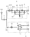
- FIG. 2 is a circuit diagram showing a configuration of the duplexer 1 according to the first embodiment of the present invention.
- the duplexer 1 is a duplexer used in the communication module 101 in FIG.
- the duplexer 1 includes an antenna terminal 7, a transmission terminal 3, a reception terminal 11, a transmission filter 5 disposed between the antenna terminal 7 and the transmission terminal 3, and between the antenna terminal 7 and the reception terminal 11. And the reception filter 6 arranged at the center.
- the transmission signal TS from the amplifier 107 is input to the transmission terminal 3, and the transmission signal TS input to the transmission terminal 3 is freed of unnecessary components other than the transmission passband in the transmission filter 5, and is applied to the antenna terminal 7. Is output.
- the reception signal RS is input from the antenna 109 to the antenna terminal 7, and unnecessary components other than the reception passband are removed by the reception filter 9 and output to the reception terminal 11.
- the transmission filter 5 is constituted by, for example, a ladder-type SAW filter.
- the transmission filter 5 is a wiring for connecting three series resonators S1, S2, and S3 connected in series between the input side and the output side, and the series resonators S1 to S3. It has three parallel resonators P1, P2, and P3 provided on a parallel arm 4b between a certain series arm 4a and a reference potential portion G. That is, the transmission filter 5 is a three-stage ladder type filter. However, the number of stages of the ladder filter in the transmission filter 5 is arbitrary.
- An inductor L is provided between the parallel resonators P1, P2, P3 and the reference potential portion G. By setting the inductance of the inductor L to a predetermined magnitude, an attenuation pole is formed outside the band of the transmission frequency of the transmission signal to increase the out-of-band attenuation.
- the plurality of series resonators S1, S2, and S3 and the plurality of parallel resonators P1, P2, and P3 are each composed of a SAW resonator.
- all of the resonators other than the series resonator S1 are composed of one SAW resonator.
- the series resonator S1 includes two SAW resonators.
- the series resonator S1 includes a SAW resonator S11 and a SAW resonator S12 connected in parallel to each other.
- the series resonator S1 can be regarded as being constituted by the two SAW resonators S11 and S12 as described above, and one SAW resonator S11 constitutes the series resonator S1, and is separated from this.
- the SAW resonators S12 can be regarded as being connected in parallel. This is because the filter design is performed by considering the two SAW resonators S11 and S12 together as one series resonator, or by performing the filter design with the two SAW resonators S11 and S12 separately. is there.
- the reception filter 9 includes, for example, a multimode SAW filter 17 and an auxiliary resonator 15 connected in series on the input side thereof.
- the multiplex mode includes a dual mode.
- the multimode SAW filter 17 has a balanced-unbalanced conversion function, and the receiving filter 9 is connected to two receiving terminals 11 from which balanced signals are output.
- the reception filter 9 is not limited to the multimode SAW filter 17 but may be a ladder filter or a filter that does not have a balanced-unbalanced conversion function.
- an impedance matching circuit made of an inductor or the like may be inserted.
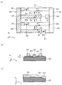
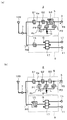
- FIG. 3 is a plan view showing a part of the SAW element 51 according to the first embodiment of the present invention.
- the SAW element 51 constitutes a ladder type filter circuit of the transmission filter 5 in the duplexer 1 shown in FIG. 2, for example, and includes the piezoelectric substrate 30 and series resonators S1 to S3 formed on the piezoelectric substrate 30. And parallel resonators P1 to P3.
- FIG. 3 shows only the series resonator S1.
- the outer periphery of the piezoelectric substrate 30 is not shown on the assumption that almost the entire surface of the paper is the main surface of the piezoelectric substrate 30.
- the SAW element 51 may be either upward or downward, but in the following, for convenience, the orthogonal coordinate system xyz is defined and the positive side in the z direction (the front side in FIG. 3). And the terms upper surface, lower surface and the like are used.
- the series resonator S1 is configured as, for example, a 1-port SAW resonator.
- the series resonator S1 is mainly composed of the piezoelectric substrate 30, the first IDT electrode 55 (S11), and the second IDT electrode 56 (S12) connected in parallel to the first IDT electrode 55.
- a signal input wiring 57 and a signal output wiring 58 are connected to the first IDT electrode 55.
- the first IDT electrode 55 is composed of a pair of first and second comb-shaped electrodes 25 and 26, and the second IDT electrode 56 is composed of a pair of third and fourth comb-shaped electrodes 27 and 28.
- the first and third comb-shaped electrodes 25 and 27 are comb-shaped electrodes on the signal input side.
- the second and fourth comb-shaped electrodes 26 and 28 are comb-shaped electrodes on the side from which signals are output.
- the series resonator S1 has reflector electrodes arranged so as to sandwich the first IDT electrode 55 and the second IDT electrode 56 from both sides in the SAW propagation direction.
- FIG. 3 shows the reflector electrodes. Is omitted. Note that the reflector electrode may not be provided.
- the series resonator S1 has a protective layer covering the IDT electrode and the like, which is not shown.
- the piezoelectric substrate 30 is a single crystal substrate having piezoelectricity, such as a lithium tantalate (LiTaO 3 ) single crystal or a lithium niobate (LiNbO 3 ) single crystal. More specifically, a 42 ° ⁇ 10 ° YX cut LiTaO 3 , a 128 ° ⁇ 10 ° YX cut LiNbO 3 substrate, or a 0 ° ⁇ 10 ° YX cut LiNbO 3 substrate is used. be able to.
- the planar shape and various dimensions of the piezoelectric substrate 30 may be set as appropriate. Note that the LiTaO 3 single crystal and the LiNbO 3 single crystal show large nonlinearity in the Z-axis direction.
- the protective layer covering the IDT electrode 55 and the like is made of an insulating material, specifically, silicon oxide, nitrogen oxide or the like.
- the pair of first and second comb-like electrodes 25 and 26 constituting the first IDT electrode 55 includes a first bus bar electrode 31, a second bus bar electrode 32, a plurality of first electrode fingers 33, and a plurality of second electrodes.
- the electrode finger 34, the plurality of first dummy electrode fingers 35, and the plurality of second dummy electrode fingers 36 are mainly configured.
- the first and second bus bar electrodes 31 and 32 are, for example, elongated and extend linearly in the SAW propagation direction (y direction) with a certain width.
- the first bus bar electrode 31 and the second bus bar electrode 32 face each other in a direction (x direction) orthogonal to the SAW propagation direction.
- the first bus bar electrode 31 and the second bus bar electrode 32 have mutually opposite inner side surfaces parallel to each other, and the distance between both side surfaces is constant in the SAW propagation direction.
- a plurality of first electrode fingers 33 and a plurality of first dummy electrode fingers 35 are connected to the first bus bar electrode 31.
- a plurality of second electrode fingers 34 and a plurality of second dummy electrode fingers 36 are connected to the second bus bar electrode 32.
- the plurality of first and second electrode fingers 33 and 34 are linearly extended in a direction (x direction) orthogonal to the SAW propagation direction with a substantially constant width.
- the plurality of first and second electrode fingers 33, 34 are arranged at regular intervals along the SAW propagation direction (y direction), and one first electrode finger 33 and one adjacent to it are arranged.
- the second electrode fingers 34 have portions adjacent to each other in the y direction.
- a region where one first electrode finger 33 and one second electrode finger 34 adjacent to the first electrode finger 33 are adjacent to each other in the y direction is defined as an intersection region Tc.
- the plurality of first and second electrode fingers 33 and 34 are provided such that the pitch p is equal to, for example, a half wavelength of the SAW wavelength ⁇ at a frequency to be resonated.
- the pitch p is defined, for example, by the center-to-center distance between one adjacent first electrode finger 33 and one second electrode finger 34.
- the wavelength ⁇ of SAW is, for example, 1.5 ⁇ m to 6 ⁇ m.
- the length and width w of one of the first and second electrode fingers 33 and 34 are set to be the same, for example. These dimensions are appropriately set according to the electrical characteristics required for the SAW element 51.
- the width w of each of the first and second electrode fingers 33 and 34 is, for example, 0.4 p to 0.7 p with respect to the pitch p of the first electrode finger 33 and the second electrode finger 34.
- the first dummy electrode finger 35 is disposed at the approximate center between the plurality of first electrode fingers 33.
- the second dummy electrode finger 36 is disposed substantially at the center between the plurality of second electrode fingers 34.
- the width of one of the first and second dummy electrode fingers 35 and 36 is equal to the width w of one of the first and second electrode fingers 33 and 34.
- the length of one of the first and second dummy electrode fingers 35 and 36 is shorter than that of the first and second electrode fingers 33 and 34.
- the first and second comb-like electrodes 25 and 26 may not have the plurality of first and second dummy electrode fingers 35 and 36.
- the tip of the first dummy electrode finger 35 is opposed to the tip of the second electrode finger 34 via the first gap 21.
- the tip of the second dummy electrode finger 36 is opposed to the tip of the first electrode finger 33 with the second gap 22 interposed therebetween.
- the number of the plurality of first gaps 21 is set to be the same as the number of the plurality of first dummy electrode fingers 35.
- the number of the plurality of second gaps 22 is set to be the same as the number of the plurality of second dummy electrode fingers 36.
- the widths of the plurality of first and second gaps 21 and 22 are the same as the width w of the plurality of first and second electrode fingers 33 and 34.
- the lengths d of the plurality of first and second gaps 21 and 22 (hereinafter sometimes referred to as gap lengths d) are the same between the plurality of first gaps 21 and the plurality of second gaps 22, The first gap 21 and the second gap 22 are the same.
- the gap lengths d of all the first and second gaps 21 and 22 are set to be the same.
- the gap length d of the first and second gaps 21 and 22 is appropriately set according to the electrical characteristics required for the SAW element 51, and is, for example, 0.1 ⁇ to 0.6 ⁇ .
- a signal input wiring 57 and a signal output wiring 58 are connected to the first IDT electrode 55.
- the signal input wiring 57 is a wiring for inputting the transmission signal TS to the first IDT electrode 55 and the second IDT electrode 56.
- This signal input wiring 57 constitutes the series arm 4a for connecting the series resonators S1 to S3 in FIG.
- the signal input wiring 57 is connected to the first bus bar electrode 31 among the first IDT electrodes 55.
- the signal output wiring 58 is a wiring for outputting the transmission signal TS from the first IDT electrode 55 and the second IDT electrode 56.
- the signal output wiring 58 constitutes the series arm 4a that connects the series resonator S1 and the antenna terminal 7 in FIG.
- the signal output wiring 58 is connected to the second bus bar electrode 32 in the first IDT electrode 55.
- the second IDT electrode 56 is connected in parallel to the first IDT electrode 55.
- the third comb-like electrode 27 is mainly composed of a third bus bar electrode 41, a plurality of third electrode fingers 43, and a plurality of third dummy electrode fingers 45.
- the fourth comb-like electrode 28 is mainly composed of a fourth bus bar electrode 42, a plurality of fourth electrode fingers 44, and a plurality of fourth dummy electrode fingers 46. Note that the third and fourth comb electrodes 27 and 28 may not have the plurality of third and fourth dummy electrode fingers 45 and 46.
- the third and fourth bus bar electrodes 41 and 42 are, for example, long and extend linearly in the SAW propagation direction (y direction) with a certain width.
- the third bus bar electrode 41 and the fourth bus bar electrode 42 are opposed to each other in the direction (x direction) orthogonal to the SAW propagation direction.
- the third bus bar electrode 41 and the fourth bus bar electrode 42 have mutually opposite inner side surfaces parallel to each other, and the distance between both side surfaces is constant in the SAW propagation direction.
- a plurality of third electrode fingers 43 and a plurality of third dummy electrode fingers 45 are connected to the third bus bar electrode 41.
- a plurality of fourth electrode fingers 44 and a plurality of fourth dummy electrode fingers 46 are connected to the fourth bus bar electrode 42.
- the plurality of third and fourth electrode fingers 43 and 44 extend in a straight line in a direction (x direction) orthogonal to the SAW propagation direction with a substantially constant width.
- the plurality of third and fourth electrode fingers 43 and 44 are arranged at regular intervals along the SAW propagation direction (y direction), and the third electrode finger 43 and the fourth electrode finger 44 adjacent thereto are arranged.
- the pitch p and width w of the third and fourth electrode fingers 43 and 44 are basically set to be the same as the pitch p and width w of the first and second electrode fingers 33 and 34.
- the third dummy electrode finger 45 is arranged at the center between the plurality of third electrode fingers 43.
- the fourth dummy electrode finger 46 is disposed at the center between the plurality of fourth electrode fingers 44.
- the widths of the third and fourth dummy electrode fingers 45 and 46 are, for example, equal to the width w of the third and fourth electrode fingers 43 and 44.
- the lengths of the third and fourth dummy electrode fingers 45 and 46 are shorter than the lengths of the third and fourth electrode fingers 43 and 44.
- the tip of the third dummy electrode finger 45 is opposed to the tip of the fourth electrode finger 44 through the third gap 23.
- the tip of the fourth dummy electrode finger 46 is opposed to the tip of the third electrode finger 43 through the fourth gap 24.
- the number of the plurality of third gaps 23 is the same as the number of the plurality of third dummy electrode fingers 45.
- the number of the plurality of fourth gaps 24 is the same as the number of the plurality of fourth dummy electrode fingers 46.
- the widths of the plurality of third and fourth gaps 23 and 24 are the same as the width w of the plurality of third and fourth electrode fingers 43 and 44.
- the gap lengths d of the plurality of third and fourth gaps 23 and 24 are, for example, the same among the plurality of third gaps 23 and between the plurality of fourth gaps 24. Are the same.
- the first IDT electrode 55 and the second IDT electrode 56 are formed so as to be approximately equal in shape and size. That is, the first IDT electrode 55 and the second IDT electrode 56 are formed such that both IDT electrodes overlap when the second IDT electrode 56 is translated and overlapped with the first IDT electrode 55 in the vertical direction.
- the shape and size of the IDT electrodes are substantially equal means that they are the same in design, and even if there is a slight difference in the shape and size of both IDT electrodes due to manufacturing variations, etc., they are included in the same range. Is.
- At least the portion excluding the bus bar electrode in the IDT electrode, that is, the shape and size of the electrode finger and the dummy electrode finger are the first IDT. It is sufficient that the electrode 55 and the second IDT electrode are substantially equal.
- the first and second IDT electrodes 55 and 56 are made of, for example, metal.
- the metal include Al or an alloy containing Al as a main component (Al alloy).
- Al alloy for example, an Al—Cu alloy can be used.
- the first and second IDT electrodes 55 and 56 may be composed of a plurality of metal layers. The thicknesses of the first and second IDT electrodes 55 and 56 may be set as appropriate. Since the first IDT electrode 55 and the second IDT electrode 56 are made of the same material and by the same process, the thicknesses of the first IDT electrode 55 and the second IDT electrode 56 are set to be substantially the same.
- the second IDT electrode 56 is connected in parallel to the first IDT electrode 55, but the series resonator S1 is configured such that the connection between the first IDT electrode 55 and the second IDT electrode 56 is different from a normal one.
- the distorted wave generated in the series resonator S1 is reduced. That is, the direction arranged from the third comb-shaped electrode 27 to the fourth comb-shaped electrode 28 is the direction arranged from the first comb-shaped electrode 25 to the second comb-shaped electrode 26.
- the first IDT electrode 55 and the second IDT electrode 56 are electrically connected to each other.
- the series resonator S1 connects the bus bar electrodes of the first and second IDT electrodes 55 and 56 to each other.
- the tip of the first electrode finger 33 is directed to the tip of the second dummy electrode finger 36 via the second gap 22, and in the second IDT electrode 56, the tip of the third electrode finger 43 is The direction toward the tip of the fourth dummy electrode finger 46 via the 4 gap 24 is opposite to the direction.
- the tip of the first dummy electrode finger 35 is directed to the tip of the second electrode finger 34 via the first gap 21, and the tip of the third dummy electrode finger 45 in the second IDT electrode 56.
- the direction toward the tip of the fourth electrode finger 44 via the third gap 23 is the opposite direction.
- the bus bar electrodes are electrically connected to each other through a connection wiring.
- the first bus bar electrode 31 is connected to the fourth bus bar electrode 42 via the first connection wiring 37
- the second bus bar electrode 32 is connected to the third bus bar electrode 41 via the second connection wiring 38. It is connected.
- the first connection wiring 37 and the second connection wiring 38 cross three-dimensionally in a region between the first IDT electrode 55 and the second IDT electrode 56. At a portion where the two connection wirings intersect, an insulating material such as a resin is interposed therebetween to prevent both connection wirings from being short-circuited.
- an insulating material such as a resin is interposed therebetween to prevent both connection wirings from being short-circuited.
- the distortion current that causes the distortion wave generated in the IDT electrode will be described. It is considered that two mechanisms, that is, electrical strain and mechanical strain, contribute to the generation of strain current in the IDT electrode.
- FIG. 5A is an enlarged view of a region V in FIG.
- the shaded second comb-like electrode 26 has a higher potential than the first comb-like electrode 25 not shaded.
- an electric field E in the direction indicated by the black arrow is generated between the first comb-like electrode 25 and the second comb-like electrode 26. That is, an electric field Ey along the SAW propagation direction (y direction) is generated in the electrode finger intersection region Tc, and the first and second gaps 21 and 22 are in a direction (x direction) orthogonal to the SAW propagation direction.
- Ey direction an electric field Ey along the SAW propagation direction
- the first and second gaps 21 and 22 are in a direction (x direction) orthogonal to the SAW propagation direction.
- the electric field Ex is generated.
- a distorted current is generated due to the non-linearity of the dielectric constant ⁇ of the piezoelectric substrate 30.
- ⁇ is a coefficient depending on the crystal orientation of the piezoelectric substrate 30. Since the direction of the strain current I 2e depends on the crystal orientation of the piezoelectric substrate 30 and is considered to be proportional to the square of the electric field E, the strain current I 2e flows in a constant direction regardless of the direction of the electric field E.
- the distorted current I 2e based on the electric field Ey in the intersection region flows in the + y direction
- the distorted current I 2e based on the electric field Ex in the gap flows in the + x direction.
- ⁇ is a positive constant
- actual ⁇ is a complex number depending on the material and crystal orientation of the piezoelectric substrate.
- the distortion current I 2e in the second gap 21 since the distortion current I 2e in the first gap 21 and the distortion current I 2e in the second gap 22 both in the same direction, they The distortion currents I 2e are not canceled out. It is considered that the distorted current I 2e remaining without canceling in this way is one of the causes of distorted waves.
- 5B is a cross-sectional view taken along the line B-B ′ of FIG. 5A
- FIG. 5C is a cross-sectional view taken along the line C-C ′ of FIG.
- the potential of the second electrode finger 34 is higher than that of the first electrode finger 33 at a certain moment.
- “+” is attached to the second electrode finger 34 having a high potential
- “ ⁇ ” is attached to the first electrode finger 33 having a low potential.
- the surface of the piezoelectric substrate 30 is deformed and undulated as shown in FIG. 5B.
- the undulation mode depends on the crystal orientation, frequency, and the like. It is conceivable that the vicinity is deformed.
- the distorted current I 2 ⁇ based on the deformation of the intersecting region Tc of the piezoelectric substrate 30 flows in the + y direction
- the distorted current I 2 ⁇ based on the deformation of the gap region flows in the + x direction.
- the distortion current I 2 ⁇ generated in the intersecting region Tc has the same magnitude and the opposite direction between the distortion current I 2 ⁇ flowing into the first electrode finger 33 and the distortion current I 2 ⁇ flowing out from the first electrode finger 33. Negate each other.
- the distorted current I 2 ⁇ generated in the intersecting region Tc cancels out. Therefore, the distortion current I 2 ⁇ in the intersecting region Tc of the IDT electrode 55 cancels out and is hardly output as a distortion wave to the outside of the SAW element 51.
- the direction in which the strain current I 2 ⁇ generated in the gap region flows is determined depending on the crystal orientation regardless of the voltage direction, and therefore flows in the same direction in the first gap 21 and the second gap 22. Therefore, the distortion current I 2 ⁇ generated in the gap region does not cancel out. Thus, the distorted current I 2 ⁇ remaining without canceling is considered to be one of the causes of the distorted wave.
- the electrode fingers of the SAW resonator Since it ranges from several tens to several hundreds, the influence of the electrode fingers positioned at both ends of the IDT electrode is small.
- FIG. 5 shows an example in which the distorted current I 2e caused by electrical strain and the distorted current I 2 ⁇ caused by mechanical strain flow in the same direction in each of the intersection region Tc and the gap region.
- the strain current I 2e and the strain current I 2 ⁇ are not necessarily in the same direction because of different generation mechanisms.
- the strain current I 2e and the strain current I 2 ⁇ may flow in opposite directions in each region.
- the cancellation occurs between the distortion current I 2e caused by electrical distortion and the distortion current I 2 ⁇ caused by mechanical distortion
- the frequency dependence of the magnitudes of both currents is greatly different. It is considered that there is almost no cancellation between the two currents, and a distorted current I 2 corresponding to the difference between the two currents is generated.
- the differential distortion current I 2 cancels out in the intersection region Tc and remains in the gap region for the same reason as described above, and eventually a distortion wave is generated.
- the distortion current I 2e caused by the electrical distortion generated in the first gap 21 and the second gap 22 and the distortion current I 2 ⁇ caused by the mechanical distortion are the causes of the distortion wave. It is thought that it is one.
- the first bus bar electrode 31 of the first IDT electrode 55 and the third bus bar electrode 41 of the second IDT electrode 56 are electrically connected, and the second bus bar electrode 32 of the first IDT electrode 55 and the second IDT electrode 55 are electrically connected. Since the electrode 56 is electrically connected to the fourth bus bar electrode 42, the distorted wave is reduced. The reason why the distorted wave is reduced in the SAW element 51 will be described in comparison with the SAW element 52 of the comparative example shown in FIG.
- the SAW element 52 of the comparative example is different from the SAW element 51 of the present embodiment only in the connection configuration of the bus bar electrodes, and the other configurations are the same.
- the SAW element 51 of the present embodiment has a staking relationship when bus bar electrodes of the same polarity constituting the first IDT electrode 55 and the second IDT electrode 56 are connected to each other.
- the SAW element 51 connects the bus bar electrodes arranged on the same side of the first IDT electrode 55 and the second IDT electrode 56.
- the first bus bar electrode 31 of the first IDT electrode 55 is electrically connected to the fourth bus bar electrode 42 of the second IDT electrode 56, and the second bus bar electrode 32 of the first IDT electrode 55 is the first bus bar electrode 32.
- the 2IDT electrode 56 is electrically connected to the third bus bar electrode 41.
- each of the first IDT electrode 55 and the second IDT electrode 56 due to the electrical strain and mechanical strain of the piezoelectric substrate 30 as described above.
- a distortion current I 2 is generated in FIG. Since a distortion current I 2 which is output from the 1IDT electrode 55 flows in the same direction as the distortion current I 2 which is output from the 2IDT electrode 56, is output to the outside without cancel each other.
- the distortion current I 2 in each of the 1IDT electrode 55 and the 2IDT electrode 56 occurs, the distortion current I 2 and the 2IDT electrode output from the 1IDT electrode 55
- the distorted currents I 2 output from 56 flow in opposite directions and cancel each other. Therefore, the distorted current I 2 output from the first IDT electrode 55 and the second IDT electrode 56 as a whole is reduced.
- the SAW element 51 since the SAW element 51 has the second IDT electrode 56 having the same shape and the same size as the first IDT electrode 55, the strain current I 2 output from the second IDT electrode 56 and the first IDT electrode 55 are output. substantially equal in magnitude to the distortion current I 2 that.
- the greater the cancellation effect of the distortion current I 2 can be suppressed greatly distorted current I 2 which is output from the entire SAW device 51 (S1).
- the strain current I 2 related to the second-order nonlinearity output from the SAW element 51 is considered to be mainly caused by the strain current I 2 generated in the gap region as described above, the first IDT electrode 55 and the number of gaps between the first 2IDT electrode 56, if the gap length d and gap width w are the same, substantially the same distortion current I 2 generated in both the IDT electrode. Therefore, when the number of gaps, the gap length d, and the gap width w are the same between the first IDT electrode 55 and the second IDT electrode 56, even if the width of the intersecting region Tc of both IDT electrodes is different, a high distortion wave reduction effect is achieved. Is obtained.
- the distortion signal can be efficiently reduced by arranging the SAW element 51 of the transmission filter 5. Since the transmission signal TS and the reception signal RS are filtered in the series resonator S1 closest to the antenna 109 in the transmission filter 5, the distortion signal is likely to increase. Therefore, the distortion wave can be reduced more efficiently by adopting the structure shown in FIG. 3 as the series resonator S1 closest to the antenna 109.
- the series resonators S2 and S3 other than the series resonator S1 and the parallel resonators P1, P2, and P3 have the same configuration as the first IDT electrode 55 that configures the SAW resonator S11, for example.
- the auxiliary resonator 15 in the reception filter 9 also has the same configuration as the first IDT electrode 55 constituting the SAW resonator S11, for example.
- FIG. 6 is a circuit diagram showing the configuration of the duplexer 2 according to the second embodiment of the present invention.
- the duplexer 2 includes a transmission filter 5 and a reception filter 9.
- the transmission filter 5 includes a piezoelectric substrate 30 and series resonators S101, S2, and S3 and parallel resonators P1, P2, and P3 formed on the piezoelectric substrate, and these constitute a ladder type filter circuit. .
- the duplexer 2 according to the second embodiment differs from the duplexer 1 according to the first embodiment only in the configuration of the series resonator disposed closest to the antenna terminal 7.
- the other configuration is the same as that of the duplexer 1.
- the series resonator S1 is composed of the SAW resonator S11 and the SAW resonator S12 connected in parallel thereto, whereas the second resonator 1 is the second resonator.
- a series resonator S101 is configured by a SAW resonator S11 and a SAW resonator S12 connected in series thereto.
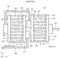
- FIG. 7 is a plan view showing a part of the SAW element 53 according to the second embodiment of the present invention, and shows only the part of the series resonator S101.
- the outer periphery of the piezoelectric substrate 30 is not shown on the assumption that almost the entire surface of the paper is the main surface of the piezoelectric substrate 30.
- the second IDT electrode 56 is connected in series to the first IDT electrode 55, but the series resonator S101 has a mode in which the connection between the first IDT electrode 55 and the second IDT electrode 56 is different from a normal one.
- the distorted wave generated in the series resonator S101 is reduced.
- the signal input wiring 57 is connected to the first bus bar electrode 31 disposed outside the two bus bar electrodes of the first IDT electrode 55.
- the signal output wiring 58 is connected to the third bus bar electrode 41 disposed inside the two bus bar electrodes of the second IDT electrode 56.
- the second bus bar electrode 32 disposed on the inner side of the two bus bar electrodes of the first IDT electrode 55 is electrically connected to the fourth bus bar electrode 42 disposed on the outer side of the two bus bar electrodes of the second IDT electrode 56.
- the first IDT electrode 55 and the second IDT electrode 56 are connected in series.
- the connection between the second bus bar electrode 32 and the fourth bus bar electrode 42 is made through the connection wiring 40.
- the tip of the first electrode finger 33 is directed to the tip of the second dummy electrode finger 36 via the second gap 22, and the tip of the third electrode finger 43 is connected to the fourth dummy electrode via the fourth gap 24.
- the direction toward the tip of the finger 46 is the same as the ⁇ x direction (left direction in the drawing).
- the tip of the first dummy electrode finger 35 is directed to the tip of the second electrode finger 34 via the first gap 21, and the tip of the third dummy electrode finger 45 is connected to the fourth electrode via the third gap 23.
- the direction toward the tip of the finger 44 is the same as the ⁇ x direction (left direction in the drawing).
- the distortion current I 2 is generated in each IDT electrode.
- the first bus bar electrode 31 is electrically connected to the signal input wiring 57
- the second bus bar electrode 32 and the fourth bus bar electrode 42 are electrically connected
- the third bus bar electrode 41 is electrically connected.
- the SAW element 54 of the comparative example is different from the SAW element 53 of the present embodiment only in the connection configuration of the bus bar electrodes and the connection configuration of the signal output wiring 58, and the other configurations are the same.
- the second bus bar electrode 32 of the second IDT electrode 56 and the fourth bus bar electrode 42 of the second IDT electrode 56 are electrically connected as described above.
- the SAW element 54 electrically connects the second bus bar electrode 32 of the first IDT electrode 55 and the third IDT electrode 41 of the second IDT electrode 56.
- the signal output wiring 58 is connected to the fourth bus bar electrode 42 of the second IDT electrode 56.
- each of the first IDT electrode 55 and the second IDT electrode 56 is caused by the electrical strain and mechanical strain of the piezoelectric substrate 30 as described above.
- a distortion current I 2 is generated in FIG. In the SAW element 53, to flow in the same direction as the distortion current I 2 which is output from the 1IDT electrode 55 and the distortion current I 2 which is output from the 2IDT electrode, is output to the outside without cancel each other.
- the distortion current I 2 in each of the 1IDT electrode 55 and the 2IDT electrode 56 occurs, the distortion current I 2 and the 2IDT electrode output from the 1IDT electrode 55 a distortion current I 2 that is output from the 56, cancel each other in order to flow in opposite directions. Therefore, the distorted current I 2 output from the first IDT electrode 55 and the second IDT electrode 56 as a whole is reduced.
- the SAW element 53 it is possible to reduce the distortion current I 2. If the second IDT electrode 56 is formed in the same shape and the same size as the first IDT electrode 55 as in the SAW element 51 according to the first embodiment, the distortion current output from the first IDT electrode 55 and the entire second IDT electrode 56 as a whole. I 2 can be greatly suppressed.
- Example 1 Two types of resonators A1 and A2 and a reference resonator R1 of Example 1 having the same configuration as the series resonator S1 (FIG. 3) of the SAW element 51 according to the first embodiment are manufactured.
- the second harmonic H2 which is a kind of distorted wave, was measured for each of the resonators.
- the reference resonator R1 is composed of one SAW resonator, and the resonators A1 and A2 of the first embodiment are shown in FIG. 3 by dividing the reference resonator R1 into two resonators. Thus, they are connected in parallel to each other.
- the resonators A1, A2, and R1 were manufactured under the conditions shown in Table 1.
- the number of electrode fingers “160/160” of the resonator A1 is the number of electrode fingers of the two SAW resonators S11 and S12 connected in parallel. That is, in the resonator A1, the SAW resonator S11 and the SAW resonator S12 each have 160 electrode fingers, and both resonators have the same size.
- the number of electrode fingers “80/80” of the resonator A2 also has the same meaning, and in the resonator A2, the two SAW resonators S11 and S12 have the same size.
- intersection width is the length of the intersection region Tc
- ⁇ is the SAW wavelength at the resonance frequency
- ⁇ 2p.
- the cross width or the number of electrode fingers of each of the SAW resonators S11 and S12 is different from the reference resonator R1, but the cross width and the number of electrode fingers in the SAW resonator S11 are different.
- the product of the intersection width and the number of electrode fingers in the SAW resonator S12 are equal to the product of the intersection width and the number of electrode fingers in the reference resonator R1. That is, the resonators A1, A2, and R1 have the same capacitance.
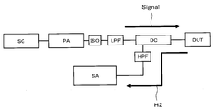
- the measurement system shown in FIG. 9 was used for the measurement of the second harmonic H2.
- SG is a signal generator
- PA is a power amplifier
- ISO is an isolator
- LPF is a low-pass filter
- DC is a directional coupler
- DUT is a SAW resonator to be measured
- HPF is a high-pass filter
- SA is a spectrum analyzer. It is.
- the resonators A1, A2, and R1 are disposed at the position of the resonator DUT.
- the measurement system shown in FIG. 9 generates a signal having a predetermined power in the signal generator SG, inputs the signal to the resonator DUT via the power amplifier PA or the like, and converts the signal into a reflected wave from the resonator DUT.
- the included second harmonic H2 is measured by the spectrum analyzer SA.
- the LPF is inserted in order to reduce unnecessary second harmonics output from the PA.
- the HPF is inserted to prevent an input signal reflected from the DUT from being input to the SA.
- the power of the input signal is 22 dBm, and the frequency is 750 to 950 MHz. Therefore, the frequency of the second harmonic is 1500 to 1900 MHz.
- the conditions regarding the measurement system are the same as those in Example 1.
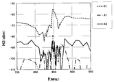
- FIG. 10 shows the measurement result of the second harmonic H2 in Example 1.
- the broken line is the measurement result of the reference resonator R ⁇ b> 1
- the alternate long and short dash line is the measurement result of the resonator A ⁇ b> 1 of Example 1
- the solid line is the measurement result of the resonator A ⁇ b> 2 of Example 1.
- the horizontal axis is the frequency of the input signal
- the vertical axis is the output value of the second harmonic H2.
- the second-order harmonics H2 of the resonators A1 and A2 of Example 1 are reduced compared to the reference resonator R1. That is, it was confirmed that the distorted wave can be reduced by the resonators A1 and A2 of Example 1.
- the resonance frequency of the used SAW resonator is about 850 MHz.
- the peak in the vicinity of 850 MHz is the contribution of the distortion current I 2 ⁇
- the constant current on the low frequency and high frequency sides is the distortion current I 2e .
- the frequency dependence of the second harmonic H2 of the reference resonator R1 is determined by the contribution of the distortion current I 2 ⁇ having a peak near the resonance frequency and the distortion current having a substantially constant value (about ⁇ 75 dBm) at all frequencies. It is a synthesis with the contribution of I 2e .
- the distorted current I 2 ⁇ and the distorted current I 2e have opposite polarities, the distorted current I 2 ⁇ and the distorted current I 2e cancel each other around the frequencies of 820 MHz and 865 MHz, and the intensity of the second harmonic H2 decreases. ing.
- the contributions of the distorted current I 2 ⁇ and the distorted current I 2e are both reduced over the entire frequency region. The same applies to Examples 2 and 3 shown below.
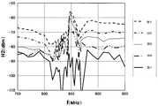
- Example 2 Four types of resonators B1, B2, B3, and B4 having the same configuration as the series resonator S1 (FIG. 3) of the SAW element 51 according to the first embodiment are manufactured, and second harmonics (H2) are produced for these resonators. ) was measured.
- the resonators B1, B2, B3, and B4 of Example 2 were manufactured under the same conditions as those shown in Table 1 except for the intersection width and the number of electrode fingers, and the intersection width was set to 18 ⁇ . . Further, the number of electrode fingers is “80/80” for the resonator B1, “96/64” for the resonator B2, and “112/48” for the resonator B3. The child B4 is “128/32”.
- the resonator B1 has the same size of the two SAW resonators S11 and S12, but the other resonators B2, B3, and B4 have different sizes of the two SAW resonators S11 and S12. ing.
- the resonator B1 is the same as the resonator A2 of the first embodiment.
- FIG. 11 shows the measurement result of the second harmonic H2 in Example 2.
- the solid line is the measurement result of the resonator B1
- the two-dot chain line is the measurement result of the resonator B2
- the dotted line is the measurement result of the resonator B3
- the one-dot chain line is the measurement result of the resonator B4.
- the measurement result of the reference resonator R1 shown in Example 1 is also indicated by a broken line in the graph.
- the second harmonic H2 is reduced in all the resonators of Example 2 compared to the reference resonator R1. It can also be seen that the second harmonic H2 is further reduced as the two SAW resonators S11 and S12 constituting the resonator of the second embodiment approach the same size. From this result, it was confirmed that the second harmonic H2 can be reduced when the two SAW resonators S11 and S12 constituting the resonator have the same size.
- Example 3 The resonator C1 having the same configuration as the series resonator S101 (FIG. 7) of the SAW element 53 according to the second embodiment, and the same configuration as the series resonator S101 of the comparative SAW element 54 shown in FIG.
- a comparative example resonator Co and a reference resonator R2 were prepared, and the second harmonic H2 was measured for these resonators.
- the resonator C1 of Example 3, the resonator Co of the comparative example, and the reference resonator R2 were manufactured under the same conditions as those shown in Table 1 except for the intersection width and the number of electrode fingers.
- the crossing width is such that both the resonator C1 has two SAW resonators S11 and S12 and 26 ⁇ , the resonator Co has two SAW resonators S11 and S12, both have 13 ⁇ , and the resonator R2 has 13 ⁇ .
- the number of electrode fingers is “100/100” for the resonator C1, “200/200” for the resonator Co, and 100 for the resonator R2.
- FIG. 12 shows the measurement result of the second harmonic H2 in Example 3.
- the solid line shows the measurement result of the resonator C1 of Example 3
- the one-dot chain line shows the measurement result of the resonator Co
- the broken line shows the measurement result of the reference resonator R2.
- the second harmonic H2 is reduced in both the resonator C1 of the example 3 and the resonator Co of the comparative example compared to the reference resonator R2.
- the reason why the second harmonic H2 of the resonator Co of the comparative example is reduced is considered to be that the voltage applied to the resonator Co is divided into two SAW resonators S11 and S12.
- the second harmonic H2 is reduced in the resonator C1 of the third embodiment more than the resonator Co of the comparative example. From this result, it was confirmed that the resonator C1 of Example 3 had a greater effect of reducing the second harmonic H2 than the resonator Co of the comparative example.
- the resonator according to the embodiment has other distortion waves caused by the second-order nonlinearity, for example, second-order intermodulation distortion (IM2). ) Etc. also exerts a reduction effect on the same principle.
- IM2 second-order intermodulation distortion
- the present invention is not limited to the above embodiment, and may be implemented in various modes.
- the example in which the first IDT electrode 55 and the second IDT electrode 56 are formed in the same shape and the same size has been described, but the shape and size of both IDT electrodes may be different, As shown in the second embodiment, the number of electrode fingers, the crossing width, and the like may be different between the first IDT electrode 55 and the second IDT electrode 56. Even in such a case, since the distortion current I 2 generated by the distortion current I 2 and the 2IDT electrode 56 generated from the 1IDT electrode 55 flows in a direction cancel each other, reducing the effect of the distortion wave is exhibited.
- first IDT electrode 55 and the second IDT electrode 56 may each have a reflector electrode 59 between the first connection wiring 37 and the second connection wiring 38 as shown in FIG. More specifically, the first IDT electrode 55 reflects an elastic wave propagating in a direction perpendicular to the direction in which the first comb-like electrode 25 and the second comb-like electrode 26 are arranged. Reflector electrodes 59a and 59b are provided so as to sandwich the first IDT electrode 55 in the propagation direction.
- the second IDT electrode 56 also has reflector electrodes 59 c and 59 d, similar to the first IDT electrode 55.
- the first IDT electrode 55 and the second IDT electrode 56 do not have the first and second dummy electrode fingers 35 and 36 and the third and fourth dummy electrode fingers 45 and 46. is there.
- the reflector electrode 59b and the reflector electrode 59c are provided in the region between the first IDT electrode 55 and the second IDT electrode 56, it is difficult for the elastic waves generated by both the IDT electrodes to interfere with each other. Can do. That is, even if the first and second IDT electrodes 55 and 56 are arranged so that the propagation direction of the elastic wave of the first IDT electrode 55 and the propagation direction of the elastic wave of the second IDT electrode 56 are aligned, they are generated by both IDT electrodes. It is possible to make the elastic wave difficult to interfere. In another aspect, since the elastic waves generated by both IDT electrodes are not easily interfered with, the first and second IDT electrodes 55 and 56 can be disposed close to each other.
- the first connection wiring 37 or the second connection wiring 38 is disposed so as to pass between the reflector electrode 59b of the first IDT electrode 55 and the reflector electrode 59c of the second IDT electrode 56. May be.
- FIG. 13A shows a case where the second connection wiring 38 passes between the reflector electrode 59b and the reflector electrode 59c.
- the connection wiring passes between the two reflector electrodes 59, so that it is possible to reduce the scattering of the elastic wave generated in the first IDT electrode 55 or the second IDT electrode 56 by the connection wiring.
- the first connection wiring 37 is arranged outside the reflector electrode 59d with respect to the second IDT electrode 56, so that the elastic wave generated in the second IDT electrode 56 is generated in the first connection. Scattering by the wiring 37 can be reduced.
- the method of connecting the first IDT electrode 55 and the second IDT electrode 56 is not limited to the above-described embodiment.
- Wiring routing is a factor that affects the electrical characteristics, size, and the like of the SAW element.
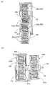
- FIGS. 14A to 14D a configuration in which the reflector electrodes of the first IDT electrode 55 and the second IDT electrode 56 are used as a part of the wiring, or the first IDT A configuration in which the reflector electrode is shared by the electrode 55 and the second IDT electrode 56 and is used as a wiring is conceivable.
- the duplexer 1 can be reduced in size.
- the number of electrode fingers of the reflectors does not interfere with the elastic waves generated by the two IDTs. It is necessary to make enough. Specifically, about 30 to 100 are required.
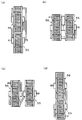
- the reflector electrodes 59a and 59d positioned outside the first IDT electrode 55 and the second IDT electrode 56 may be electrically connected to the first IDT electrode 55 or the second IDT electrode 56 as shown in FIG.
- the hatched portions are portions having the same electrical polarity. Note that a portion where the signal input wiring 57 and the signal output wiring 58 are connected is indicated by a dotted line.
- reflector electrodes 59 b and 59 c arranged between the first IDT electrode 55 and the second IDT electrode 56 shown in FIG. 13A are used as a common reflector electrode 59. And used as part of the first connection wiring 37.
- the first comb-like electrode 25 and the reflector electrode 59 located between the first and second IDT electrodes 55 and 56 are connected using the first bus bar electrode 31.
- the reflector electrode 59 located between the first and second IDT electrodes 55 and 56 and the third comb-like electrode 27 are connected using the third bus bar electrode 41.
- the second comb-like electrode 26 and the fourth comb-like electrode 28 are electrically connected via a reflector electrode 59a.
- the fourth comb-shaped electrode 28 and the reflector electrode 59 d are electrically connected via the fourth bus bar electrode 42.
- the first, second, third, and fourth comb-like electrodes 25, 26, 27, and 28 are reflector electrodes in which the electrode fingers located at the ends in the propagation direction of the elastic wave have polarity. It is adjacent to 59 mag. For this reason, due to the nonlinearity in the thickness (depth) direction, it is possible to generate strain currents I 3 due to strain generated at the ends of the IDT electrodes in which the period of the electrode fingers is asymmetric in the directions that cancel each other. In addition, the strain current I 3 flowing through the SAW element 51 can be reduced.
- the distorted wave generated due to the thickness direction depends on the polarity of the adjacent electrode finger or reflector electrode.
- the first electrode finger 33 located at the end other than the end of the first comb-like electrode 25 is symmetrically arranged on both sides, and the second electrode fingers 34 having different polarities are adjacent to each other. Therefore, there is almost no distortion wave generated due to the thickness direction.
- the first electrode finger 33 located at the end has a second electrode finger 34 adjacent to one end and the other electrode having the same polarity as the second electrode finger 34.
- 59a is arranged.
- the contact area with the piezoelectric substrate 30 is larger in the reflector electrode 59a and is asymmetrical. . For this reason, the generated distortion is not completely canceled, and a substantial distortion current is generated.
- the contact area with the piezoelectric substrate 30 is the first. Since the connection wiring 37 and the first electrode finger 33 are large and asymmetric, substantial distortion current is generated. However, the polarity is opposite to that generated at the end on the reflector electrode 59a side.
- the strain currents I3 cancel each other, and the influence of the strain generated at the electrode finger end portion of the first IDT electrode can be reduced.
- the reflector electrode 59 is used as the second connection wiring 38 for connecting the first IDT electrode 55 and the second IDT electrode 56.
- the second electrode finger 34 of the electrode 26 may be used.
- the second electrode finger 34 can also be regarded as a reflector electrode 59 in a broad sense.
- the hatched portions are portions having the same electrical polarity.
- the SAW element 51 can be reduced in size.
- the electrode fingers (second electrode finger 34 and fourth electrode finger 43) adjacent to the first connection wiring 37 are arranged so as to have a different polarity from the first connection wiring 37, thereby generating the first IDT electrode 55.
- the phase of the elastic wave and the elastic wave generated by the second IDT electrode 56 can be matched, and interference that degrades the impedance characteristics can be reduced.
- the size may be further reduced by adjusting the electrode finger located at the end of the comb-like electrode.
- the hatched portions are portions having the same polarity. Specifically, of the first IDT electrode 55, the electrode finger (first electrode finger 33) adjacent to the second IDT electrode 56 and the electrode finger of the second IDT electrode 56 adjacent to the first IDT electrode 55 (fourth electrode finger 43). ) And have different polarities. By arranging in this way, the phase of the elastic wave generated at the first IDT electrode 55 and the elastic wave generated at the second IDT electrode 56 can be aligned, and interference that degrades impedance characteristics is reduced. can do.
- a reflector electrode 59 having a smaller number of electrode fingers than that described in FIG. 14 may be disposed between the first IDT electrode 55 and the second IDT electrode 56.
- the first IDT electrode 55 is disposed in consideration of the polarities of the electrode finger on the second IDT electrode 56 side and the electrode finger on the first IDT electrode 55 side in the second IDT electrode 56.
- the electrode fingers of the reflector electrodes 59c and 59d located between the first IDT electrode 55 and the second IDT electrode 56 are set to be an even number.
- the polarity of the first electrode finger 33 on the second IDT electrode 56 side of the first IDT electrode 55 and the polarity of the fourth electrode finger 44 on the first IDT electrode 55 side of the second IDT electrode 56 are the same.
- the electrode fingers of the reflector electrodes 59c and 59d located between the first IDT electrode 55 and the second IDT electrode 56 are set to be an odd number.
- the number can be significantly reduced from 30 to 100 described in FIG. Specifically, the number can be 0 (example in FIG. 16) to 30. As a result, it is possible to provide a resonator that is smaller, generates less distortion, and has no deterioration in impedance characteristics. In this example, only the case where the two IDT electrodes 55 and 56 are connected in parallel has been described. However, as shown in FIG.
- the acoustic wave element is not limited to a SAW element (in a narrow sense).
- the SAW element may be a boundary acoustic wave element, for example.
- the SAW element has a plurality of resonators and configures a filter circuit.
- the SAW element may be configured by only one resonator.
- the shape of the IDT electrode is not limited to that shown in the figure.
- the IDT electrode may not be provided with a dummy electrode finger, for example.
- the electrode fingers may be apodized by changing the cross width of the electrode fingers along the SAW propagation direction.
- the IDT electrode may be one in which the bus bar electrode is inclined or bent, and the size in the direction (y direction) orthogonal to the propagation direction of the elastic wave of the bus bar electrode changes (on the electrode finger side of the bus bar). The position of the edge in the y direction may be changed).
- the IDT electrode is provided with a portion where the pitch of the electrode fingers is narrowed, or two or more electrode fingers extending from one comb-like electrode are adjacent to each other without sandwiching an electrode finger extending from the other comb-like electrode. A portion may be provided.
- the direction in which the third comb-teeth electrode 27 is arranged toward the fourth comb-teeth electrode 28 is directed from the first comb-teeth electrode 25 to the second comb-teeth electrode 26.
- the present invention is not limited to this configuration. That is, the direction arranged from the third comb-shaped electrode 27 to the fourth comb-shaped electrode 28 is the direction arranged from the first comb-shaped electrode 25 to the second comb-shaped electrode 26. If it is not the same direction (form of FIG. 4, form of FIG. 8) (if different), there is an effect of reducing distortion waves.
- the direction from the third comb-like electrode 27 to the fourth comb-like electrode 28 is arranged from the first comb-like electrode 25 to the second comb-like electrode 26. It is only necessary to deviate from the direction in which it is located. By arranging in this way, the distortion current canceling effect is exhibited, and the distortion current output from the SAW element 51 can be reduced.
- the SAW element 51 is divided in the above-described embodiment, as shown in FIGS. 20 and 21, the series resonators S1 to S3, the parallel resonators P1 to P3, or the auxiliary resonance constituting the duplexer 1 are used.
- the distorted wave may be reduced between the children 15.
- the parallel resonator P1 of the transmission filter 5 is arranged from the comb-like electrode on the signal input side to the comb-like electrode on the signal output side with respect to the series resonators S1 to S3.
- the distorted wave generated in the series resonators S1 to S3 and the distorted wave generated in the parallel resonator P1 can be canceled out.
- distorted waves in the transmission filter 5 can be reduced.
- At least one of the parallel resonators P1 to P3 is different from the series resonators S1 to S3 in the arrangement direction of the comb-like electrodes on the signal output side from the comb-like electrodes on the signal input side. What is necessary is just to arrange
- the arrangement direction of the series resonator S3 is different from that of the series resonator S1 or S2 from the comb-like electrode on the signal input side to the comb-like electrode on the signal output side. You may arrange
- the configuration of the present embodiment is applied to the series resonator S3.
- the same configuration can be appropriately applied to the series resonator S2 or S3. By arranging in this way, distorted waves can be reduced.
- the auxiliary resonator 15 disposed in the reception filter 6 is output from the comb-like electrode on the signal input side with respect to the series resonators S1 to S3 of the transmission filter 5.
Landscapes
- Physics & Mathematics (AREA)
- Acoustics & Sound (AREA)
- Electromagnetism (AREA)
- Surface Acoustic Wave Elements And Circuit Networks Thereof (AREA)
Priority Applications (5)
| Application Number | Priority Date | Filing Date | Title |
|---|---|---|---|
| CN201480008725.3A CN104995836B (zh) | 2013-02-27 | 2014-02-27 | 弹性波元件、分波器以及通信模块 |
| EP14757259.8A EP2963819B1 (en) | 2013-02-27 | 2014-02-27 | Elastic wave element, demultiplexer and communication module |
| JP2015503021A JP5844939B2 (ja) | 2013-02-27 | 2014-02-27 | 弾性波素子、分波器および通信モジュール |
| US14/836,782 US9806692B2 (en) | 2013-02-27 | 2015-08-26 | Acoustic wave element, duplexer, and communication module |
| US15/794,705 US10541672B2 (en) | 2013-02-27 | 2017-10-26 | Acoustic wave element, duplexer, and communication module |
Applications Claiming Priority (4)
| Application Number | Priority Date | Filing Date | Title |
|---|---|---|---|
| JP2013-036663 | 2013-02-27 | ||
| JP2013036663 | 2013-02-27 | ||
| JP2013-227484 | 2013-10-31 | ||
| JP2013227484 | 2013-10-31 |
Related Child Applications (1)
| Application Number | Title | Priority Date | Filing Date |
|---|---|---|---|
| US14/836,782 Continuation-In-Part US9806692B2 (en) | 2013-02-27 | 2015-08-26 | Acoustic wave element, duplexer, and communication module |
Publications (1)
| Publication Number | Publication Date |
|---|---|
| WO2014133084A1 true WO2014133084A1 (ja) | 2014-09-04 |
Family
ID=51428343
Family Applications (1)
| Application Number | Title | Priority Date | Filing Date |
|---|---|---|---|
| PCT/JP2014/054889 Ceased WO2014133084A1 (ja) | 2013-02-27 | 2014-02-27 | 弾性波素子、分波器および通信モジュール |
Country Status (5)
| Country | Link |
|---|---|
| US (2) | US9806692B2 (enExample) |
| EP (1) | EP2963819B1 (enExample) |
| JP (3) | JP5844939B2 (enExample) |
| CN (1) | CN104995836B (enExample) |
| WO (1) | WO2014133084A1 (enExample) |
Cited By (11)
| Publication number | Priority date | Publication date | Assignee | Title |
|---|---|---|---|---|
| WO2016056384A1 (ja) * | 2014-10-06 | 2016-04-14 | 株式会社村田製作所 | ラダー型フィルタ及びデュプレクサ |
| US20160118956A1 (en) * | 2013-07-02 | 2016-04-28 | Murata Manufacturing Co., Ltd. | Surface acoustic wave resonator and surface acoustic wave filter device |
| WO2018117059A1 (ja) * | 2016-12-19 | 2018-06-28 | 株式会社村田製作所 | 弾性波共振器、フィルタ装置およびマルチプレクサ |
| WO2018117060A1 (ja) * | 2016-12-19 | 2018-06-28 | 株式会社村田製作所 | 弾性波共振器、フィルタ装置およびマルチプレクサ |
| US10090823B2 (en) | 2014-10-21 | 2018-10-02 | Murata Manufacturing Co., Ltd. | Elastic wave resonator and ladder filter |
| CN108886351A (zh) * | 2016-03-31 | 2018-11-23 | 京瓷株式会社 | 弹性波元件以及通信装置 |
| US10622969B2 (en) | 2014-12-02 | 2020-04-14 | Kyocera Corporation | Acoustic wave element, multi plexer, and communication module |
| WO2020129470A1 (ja) * | 2018-12-20 | 2020-06-25 | 株式会社村田製作所 | マルチプレクサ |
| JP2021036706A (ja) * | 2015-03-31 | 2021-03-04 | 京セラ株式会社 | 弾性波モジュール |
| WO2021049206A1 (ja) * | 2019-09-13 | 2021-03-18 | 株式会社村田製作所 | 弾性波フィルタ |
| WO2025100314A1 (ja) * | 2023-11-09 | 2025-05-15 | 株式会社村田製作所 | 弾性波装置 |
Families Citing this family (94)
| Publication number | Priority date | Publication date | Assignee | Title |
|---|---|---|---|---|
| WO2014133084A1 (ja) * | 2013-02-27 | 2014-09-04 | 京セラ株式会社 | 弾性波素子、分波器および通信モジュール |
| WO2015033892A1 (ja) * | 2013-09-06 | 2015-03-12 | 株式会社村田製作所 | 弾性波共振子、弾性波フィルタ装置及びデュプレクサ |
| JP6441590B2 (ja) * | 2014-05-23 | 2018-12-19 | 太陽誘電株式会社 | 弾性波デバイス |
| US9502343B1 (en) * | 2015-09-18 | 2016-11-22 | Taiwan Semiconductor Manufacturing Company, Ltd. | Dummy metal with zigzagged edges |
| DE102016114071B3 (de) * | 2016-07-29 | 2018-01-25 | Snaptrack, Inc. | Elektroakustisches Filter mit reduzierten Plattenmoden |
| CN106549648A (zh) * | 2016-12-06 | 2017-03-29 | 深圳市麦高锐科技有限公司 | 一种芯片级封装的声表面波谐振器及制作工艺 |
| WO2018110057A1 (ja) * | 2016-12-16 | 2018-06-21 | 株式会社村田製作所 | 弾性波装置、高周波フロントエンド回路及び通信装置 |
| KR102291881B1 (ko) * | 2017-02-03 | 2021-08-19 | 가부시키가이샤 무라타 세이사쿠쇼 | 탄성 표면파 장치 |
| DE102017110233A1 (de) * | 2017-05-11 | 2018-11-15 | RF360 Europe GmbH | SAW-Vorrichtung mit unterdrücktem Parasitärsignal |
| CN111684719B (zh) * | 2018-02-05 | 2023-07-25 | 株式会社村田制作所 | 滤波器装置、高频前端电路、以及通信装置 |
| US12237826B2 (en) | 2018-06-15 | 2025-02-25 | Murata Manufacturing Co., Ltd. | Transversely-excited film bulk acoustic resonator with optimized electrode thickness, mark, and pitch |
| US11929731B2 (en) | 2018-02-18 | 2024-03-12 | Murata Manufacturing Co., Ltd. | Transversely-excited film bulk acoustic resonator with optimized electrode mark, and pitch |
| US10601392B2 (en) | 2018-06-15 | 2020-03-24 | Resonant Inc. | Solidly-mounted transversely-excited film bulk acoustic resonator |
| US11206009B2 (en) | 2019-08-28 | 2021-12-21 | Resonant Inc. | Transversely-excited film bulk acoustic resonator with interdigital transducer with varied mark and pitch |
| US10911023B2 (en) | 2018-06-15 | 2021-02-02 | Resonant Inc. | Transversely-excited film bulk acoustic resonator with etch-stop layer |
| US11146232B2 (en) | 2018-06-15 | 2021-10-12 | Resonant Inc. | Transversely-excited film bulk acoustic resonator with reduced spurious modes |
| US11509279B2 (en) | 2020-07-18 | 2022-11-22 | Resonant Inc. | Acoustic resonators and filters with reduced temperature coefficient of frequency |
| US11323090B2 (en) | 2018-06-15 | 2022-05-03 | Resonant Inc. | Transversely-excited film bulk acoustic resonator using Y-X-cut lithium niobate for high power applications |
| US11936358B2 (en) | 2020-11-11 | 2024-03-19 | Murata Manufacturing Co., Ltd. | Transversely-excited film bulk acoustic resonator with low thermal impedance |
| US10637438B2 (en) | 2018-06-15 | 2020-04-28 | Resonant Inc. | Transversely-excited film bulk acoustic resonators for high power applications |
| US11323089B2 (en) | 2018-06-15 | 2022-05-03 | Resonant Inc. | Filter using piezoelectric film bonded to high resistivity silicon substrate with trap-rich layer |
| US12088281B2 (en) | 2021-02-03 | 2024-09-10 | Murata Manufacturing Co., Ltd. | Transversely-excited film bulk acoustic resonator with multi-mark interdigital transducer |
| US12040779B2 (en) | 2020-04-20 | 2024-07-16 | Murata Manufacturing Co., Ltd. | Small transversely-excited film bulk acoustic resonators with enhanced Q-factor |
| US11323096B2 (en) | 2018-06-15 | 2022-05-03 | Resonant Inc. | Transversely-excited film bulk acoustic resonator with periodic etched holes |
| US11888463B2 (en) | 2018-06-15 | 2024-01-30 | Murata Manufacturing Co., Ltd. | Multi-port filter using transversely-excited film bulk acoustic resonators |
| US11901878B2 (en) | 2018-06-15 | 2024-02-13 | Murata Manufacturing Co., Ltd. | Transversely-excited film bulk acoustic resonators with two-layer electrodes with a wider top layer |
| US10826462B2 (en) | 2018-06-15 | 2020-11-03 | Resonant Inc. | Transversely-excited film bulk acoustic resonators with molybdenum conductors |
| US11329628B2 (en) | 2020-06-17 | 2022-05-10 | Resonant Inc. | Filter using lithium niobate and lithium tantalate transversely-excited film bulk acoustic resonators |
| US11323091B2 (en) | 2018-06-15 | 2022-05-03 | Resonant Inc. | Transversely-excited film bulk acoustic resonator with diaphragm support pedestals |
| US12095446B2 (en) | 2018-06-15 | 2024-09-17 | Murata Manufacturing Co., Ltd. | Transversely-excited film bulk acoustic resonator with optimized electrode thickness, mark, and pitch |
| US10992284B2 (en) | 2018-06-15 | 2021-04-27 | Resonant Inc. | Filter using transversely-excited film bulk acoustic resonators with multiple frequency setting layers |
| US12113512B2 (en) | 2021-03-29 | 2024-10-08 | Murata Manufacturing Co., Ltd. | Layout of XBARs with multiple sub-resonators in parallel |
| US12218650B2 (en) | 2018-06-15 | 2025-02-04 | Murata Manufacturing Co., Ltd. | Transversely-excited film bulk acoustic resonator |
| US12040781B2 (en) | 2018-06-15 | 2024-07-16 | Murata Manufacturing Co., Ltd. | Transversely-excited film bulk acoustic resonator package |
| US12149227B2 (en) | 2018-06-15 | 2024-11-19 | Murata Manufacturing Co., Ltd. | Transversely-excited film bulk acoustic resonator package |
| US10998882B2 (en) | 2018-06-15 | 2021-05-04 | Resonant Inc. | XBAR resonators with non-rectangular diaphragms |
| US11870423B2 (en) | 2018-06-15 | 2024-01-09 | Murata Manufacturing Co., Ltd. | Wide bandwidth temperature-compensated transversely-excited film bulk acoustic resonator |
| US10917072B2 (en) | 2019-06-24 | 2021-02-09 | Resonant Inc. | Split ladder acoustic wave filters |
| US12191838B2 (en) | 2018-06-15 | 2025-01-07 | Murata Manufacturing Co., Ltd. | Solidly-mounted transversely-excited film bulk acoustic device and method |
| US12244295B2 (en) | 2018-06-15 | 2025-03-04 | Murata Manufacturing Co., Ltd. | Transversely-excited film bulk acoustic resonators with two-layer electrodes having a narrower top layer |
| US12283944B2 (en) | 2018-06-15 | 2025-04-22 | Murata Manufacturing Co., Ltd. | Transversely-excited film bulk acoustic resonator with recessed rotated-Y-X cut lithium niobate |
| US11916539B2 (en) | 2020-02-28 | 2024-02-27 | Murata Manufacturing Co., Ltd. | Split-ladder band N77 filter using transversely-excited film bulk acoustic resonators |
| US12212306B2 (en) | 2018-06-15 | 2025-01-28 | Murata Manufacturing Co., Ltd. | Transversely-excited film bulk acoustic resonator with multiple diaphragm thicknesses and fabrication method |
| US12155374B2 (en) | 2021-04-02 | 2024-11-26 | Murata Manufacturing Co., Ltd. | Tiled transversely-excited film bulk acoustic resonator high power filters |
| US12170516B2 (en) | 2018-06-15 | 2024-12-17 | Murata Manufacturing Co., Ltd. | Filters using transversly-excited film bulk acoustic resonators with frequency-setting dielectric layers |
| US10985728B2 (en) | 2018-06-15 | 2021-04-20 | Resonant Inc. | Transversely-excited film bulk acoustic resonator and filter with a uniform-thickness dielectric overlayer |
| US11349452B2 (en) | 2018-06-15 | 2022-05-31 | Resonant Inc. | Transversely-excited film bulk acoustic filters with symmetric layout |
| US11264966B2 (en) | 2018-06-15 | 2022-03-01 | Resonant Inc. | Solidly-mounted transversely-excited film bulk acoustic resonator with diamond layers in Bragg reflector stack |
| US11996822B2 (en) | 2018-06-15 | 2024-05-28 | Murata Manufacturing Co., Ltd. | Wide bandwidth time division duplex transceiver |
| US11146238B2 (en) | 2018-06-15 | 2021-10-12 | Resonant Inc. | Film bulk acoustic resonator fabrication method |
| US12095441B2 (en) | 2018-06-15 | 2024-09-17 | Murata Manufacturing Co., Ltd. | Transversely excited film bulk acoustic resonator with recessed interdigital transducer fingers |
| US12155371B2 (en) | 2021-03-29 | 2024-11-26 | Murata Manufacturing Co., Ltd. | Layout of xbars with multiple sub-resonators in series |
| US11876498B2 (en) | 2018-06-15 | 2024-01-16 | Murata Manufacturing Co., Ltd. | Transversely-excited film bulk acoustic resonator with multiple diaphragm thicknesses and fabrication method |
| US12224732B2 (en) | 2018-06-15 | 2025-02-11 | Murata Manufacturing Co., Ltd. | Solidly-mounted transversely-excited film bulk acoustic resonators and filters for 27 GHz communications bands |
| US11949402B2 (en) | 2020-08-31 | 2024-04-02 | Murata Manufacturing Co., Ltd. | Resonators with different membrane thicknesses on the same die |
| US11909381B2 (en) | 2018-06-15 | 2024-02-20 | Murata Manufacturing Co., Ltd. | Transversely-excited film bulk acoustic resonators with two-layer electrodes having a narrower top layer |
| US12191837B2 (en) | 2018-06-15 | 2025-01-07 | Murata Manufacturing Co., Ltd. | Solidly-mounted transversely-excited film bulk acoustic device |
| US11967945B2 (en) | 2018-06-15 | 2024-04-23 | Murata Manufacturing Co., Ltd. | Transversly-excited film bulk acoustic resonators and filters |
| US12119808B2 (en) | 2018-06-15 | 2024-10-15 | Murata Manufacturing Co., Ltd. | Transversely-excited film bulk acoustic resonator package |
| US10819309B1 (en) | 2019-04-05 | 2020-10-27 | Resonant Inc. | Transversely-excited film bulk acoustic resonator package and method |
| US12081187B2 (en) | 2018-06-15 | 2024-09-03 | Murata Manufacturing Co., Ltd. | Transversely-excited film bulk acoustic resonator |
| US11996825B2 (en) | 2020-06-17 | 2024-05-28 | Murata Manufacturing Co., Ltd. | Filter using lithium niobate and rotated lithium tantalate transversely-excited film bulk acoustic resonators |
| US12301212B2 (en) | 2018-06-15 | 2025-05-13 | Murata Manufacturing Co., Ltd. | XBAR resonators with non-rectangular diaphragms |
| US12184261B2 (en) | 2018-06-15 | 2024-12-31 | Murata Manufacturing Co., Ltd. | Transversely-excited film bulk acoustic resonator with a cavity having round end zones |
| US12375056B2 (en) | 2018-06-15 | 2025-07-29 | Murata Manufacturing Co., Ltd. | Transversely-excited film bulk acoustic resonators |
| DE112019005403T5 (de) | 2018-10-31 | 2021-07-15 | Resonant Inc. | Fest montierter transversal angeregter akustischer filmvolumenresonator |
| WO2020184641A1 (ja) * | 2019-03-13 | 2020-09-17 | 株式会社村田製作所 | 弾性波フィルタ装置およびマルチプレクサ |
| CN113615083B (zh) | 2019-03-14 | 2024-10-15 | 株式会社村田制作所 | 带有半λ介电层的横向激励的薄膜体声学谐振器 |
| US11563418B2 (en) | 2019-03-25 | 2023-01-24 | Skyworks Solutions, Inc. | Methods of manufacturing acoustic wave resonators with isolation |
| DE102019108852B4 (de) * | 2019-04-04 | 2021-09-09 | RF360 Europe GmbH | Mikroakustisches Bandsperrfilter |
| CN114424458A (zh) * | 2019-09-27 | 2022-04-29 | 株式会社村田制作所 | 弹性波装置 |
| US11881836B2 (en) * | 2019-11-25 | 2024-01-23 | Skyworks Solutions, Inc. | Cascaded resonator with different reflector pitch |
| JP7491087B2 (ja) * | 2019-12-11 | 2024-05-28 | 株式会社村田製作所 | フィルタ装置 |
| US12506462B2 (en) | 2020-02-28 | 2025-12-23 | Murata Manufacturing Co., Ltd. | Transversely-excited film bulk acoustic resonator with multi-pitch interdigital transducer |
| US12255625B2 (en) | 2020-02-28 | 2025-03-18 | Murata Manufacturing Co., Ltd. | Filter using transversely-excited film bulk acoustic resonators with inductively coupled sub-resonators |
| US12341493B2 (en) | 2020-04-20 | 2025-06-24 | Murata Manufacturing Co., Ltd. | Low loss transversely-excited film bulk acoustic resonators and filters |
| US12341490B2 (en) | 2020-04-20 | 2025-06-24 | Murata Manufacturing Co., Ltd. | Low loss transversely-excited film bulk acoustic resonators and filters |
| US12278617B2 (en) | 2020-04-20 | 2025-04-15 | Murata Manufacturing Co., Ltd. | High Q solidly-mounted transversely-excited film bulk acoustic resonators |
| US11811391B2 (en) | 2020-05-04 | 2023-11-07 | Murata Manufacturing Co., Ltd. | Transversely-excited film bulk acoustic resonator with etched conductor patterns |
| US10992282B1 (en) | 2020-06-18 | 2021-04-27 | Resonant Inc. | Transversely-excited film bulk acoustic resonators with electrodes having a second layer of variable width |
| US11742828B2 (en) | 2020-06-30 | 2023-08-29 | Murata Manufacturing Co., Ltd. | Transversely-excited film bulk acoustic resonator with symmetric diaphragm |
| CN116097565A (zh) * | 2020-08-28 | 2023-05-09 | 京瓷株式会社 | 弹性波元件以及通信装置 |
| KR102825987B1 (ko) * | 2020-09-29 | 2025-06-26 | 가부시키가이샤 무라타 세이사쿠쇼 | 종결합 공진자형 탄성파 필터 및 탄성파 필터 |
| US11405019B2 (en) | 2020-10-05 | 2022-08-02 | Resonant Inc. | Transversely-excited film bulk acoustic resonator matrix filters |
| US11405017B2 (en) | 2020-10-05 | 2022-08-02 | Resonant Inc. | Acoustic matrix filters and radios using acoustic matrix filters |
| US12003226B2 (en) | 2020-11-11 | 2024-06-04 | Murata Manufacturing Co., Ltd | Transversely-excited film bulk acoustic resonator with low thermal impedance |
| US11239816B1 (en) | 2021-01-15 | 2022-02-01 | Resonant Inc. | Decoupled transversely-excited film bulk acoustic resonators |
| US12166468B2 (en) | 2021-01-15 | 2024-12-10 | Murata Manufacturing Co., Ltd. | Decoupled transversely-excited film bulk acoustic resonators for high power filters |
| JP7416126B2 (ja) * | 2021-06-03 | 2024-01-17 | 株式会社村田製作所 | 低損失横方向励起フィルムバルク音響共振器及びフィルタ |
| US12424999B2 (en) | 2021-12-28 | 2025-09-23 | Murata Manufacturing Co., Ltd. | Transversely-excited film bulk acoustic resonators with gap dielectric stripes in busbar-electrode gaps |
| US12413196B2 (en) | 2022-02-16 | 2025-09-09 | Murata Manufacturing Co., Ltd. | Tuning acoustic resonators with back-side coating |
| US12549151B2 (en) | 2022-04-12 | 2026-02-10 | Murata Manufacturing Co., Ltd. | Transversely-excited film bulk acoustic resonator with thick dielectric layer for improved coupling |
| WO2024085127A1 (ja) * | 2022-10-17 | 2024-04-25 | 株式会社村田製作所 | 弾性波装置 |
| US12489415B2 (en) | 2022-10-19 | 2025-12-02 | Murata Manufacturing Co., Ltd. | Acoustic resonator lid for thermal transport |
Citations (6)
| Publication number | Priority date | Publication date | Assignee | Title |
|---|---|---|---|---|
| JP2006080873A (ja) * | 2004-09-09 | 2006-03-23 | Hitachi Media Electoronics Co Ltd | 弾性表面波装置及びそれを用いた通信装置 |
| JP2007019975A (ja) * | 2005-07-08 | 2007-01-25 | Epson Toyocom Corp | 弾性表面波デバイス、モジュール装置、発振回路 |
| JP2007074698A (ja) | 2005-08-08 | 2007-03-22 | Fujitsu Media Device Kk | 分波器及びラダー型フィルタ |
| JP2010021914A (ja) * | 2008-07-14 | 2010-01-28 | Murata Mfg Co Ltd | 分波器 |
| JP2010278830A (ja) * | 2009-05-29 | 2010-12-09 | Murata Mfg Co Ltd | ラダー型フィルタ及びその製造方法並びにデュプレクサ |
| JP2012147175A (ja) * | 2011-01-11 | 2012-08-02 | Murata Mfg Co Ltd | 弾性波分波器 |
Family Cites Families (22)
| Publication number | Priority date | Publication date | Assignee | Title |
|---|---|---|---|---|
| GB2033185B (en) * | 1978-09-22 | 1983-05-18 | Secr Defence | Acoustic wave device with temperature stabilisation |
| JP3360541B2 (ja) * | 1995-10-20 | 2002-12-24 | セイコーエプソン株式会社 | 弾性表面波装置及びその設計方法 |
| JP2000031778A (ja) * | 1998-07-14 | 2000-01-28 | Toyo Commun Equip Co Ltd | ラダー型sawフィルタ |
| JP3440935B2 (ja) * | 2000-11-29 | 2003-08-25 | 株式会社村田製作所 | 弾性表面波フィルタ |
| US6557776B2 (en) * | 2001-07-19 | 2003-05-06 | Cummins Inc. | Fuel injector with injection rate control |
| JP3846409B2 (ja) * | 2002-02-15 | 2006-11-15 | 株式会社村田製作所 | 弾性表面波装置、通信装置 |
| WO2005101657A1 (ja) * | 2004-04-16 | 2005-10-27 | Toyo Communication Equipment Co., Ltd. | 平衡型弾性表面波フィルタ |
| DE102004020183B4 (de) * | 2004-04-22 | 2015-12-03 | Epcos Ag | Oberflächenwellen-Resonatorfilter mit longitudinal gekoppelten Wandlern |
| JP2006013576A (ja) * | 2004-06-22 | 2006-01-12 | Epson Toyocom Corp | Sawデバイスとこれを用いた装置 |
| JP2007208690A (ja) | 2006-02-02 | 2007-08-16 | Epson Toyocom Corp | 弾性表面波素子および発振器 |
| JP5036435B2 (ja) * | 2006-09-01 | 2012-09-26 | 太陽誘電株式会社 | 弾性波デバイス、フィルタおよび分波器 |
| WO2008140551A2 (en) * | 2006-10-16 | 2008-11-20 | Pioneer Surgical Technology, Inc. | Fusion device |
| WO2009131227A1 (ja) * | 2008-04-25 | 2009-10-29 | 京セラ株式会社 | 弾性表面波装置およびそれを用いた通信装置 |
| JP5206128B2 (ja) * | 2008-06-03 | 2013-06-12 | 株式会社村田製作所 | 弾性波装置及びその製造方法 |
| JP2010103951A (ja) * | 2008-10-27 | 2010-05-06 | Epson Toyocom Corp | Saw共振片 |
| JP5056952B2 (ja) * | 2008-11-04 | 2012-10-24 | 株式会社村田製作所 | 弾性波フィルタ装置および、それを備えるモジュール |
| JP5100890B2 (ja) * | 2009-06-26 | 2012-12-19 | 京セラ株式会社 | 弾性表面波フィルタおよびそれを用いた分波器 |
| JP5394847B2 (ja) * | 2009-08-06 | 2014-01-22 | 太陽誘電株式会社 | 分波器 |
| WO2011024876A1 (ja) * | 2009-08-25 | 2011-03-03 | 京セラ株式会社 | 弾性表面波装置 |
| JP2012010164A (ja) * | 2010-06-25 | 2012-01-12 | Murata Mfg Co Ltd | 弾性波分波器 |
| WO2014133084A1 (ja) * | 2013-02-27 | 2014-09-04 | 京セラ株式会社 | 弾性波素子、分波器および通信モジュール |
| JPWO2015002047A1 (ja) * | 2013-07-02 | 2017-02-23 | 株式会社村田製作所 | 弾性表面波共振器及び弾性表面波フィルタ装置 |
-
2014
- 2014-02-27 WO PCT/JP2014/054889 patent/WO2014133084A1/ja not_active Ceased
- 2014-02-27 JP JP2015503021A patent/JP5844939B2/ja active Active
- 2014-02-27 CN CN201480008725.3A patent/CN104995836B/zh active Active
- 2014-02-27 EP EP14757259.8A patent/EP2963819B1/en active Active
-
2015
- 2015-08-26 US US14/836,782 patent/US9806692B2/en active Active
- 2015-09-17 JP JP2015184358A patent/JP6100852B2/ja active Active
-
2017
- 2017-02-23 JP JP2017032319A patent/JP6426776B2/ja active Active
- 2017-10-26 US US15/794,705 patent/US10541672B2/en active Active
Patent Citations (6)
| Publication number | Priority date | Publication date | Assignee | Title |
|---|---|---|---|---|
| JP2006080873A (ja) * | 2004-09-09 | 2006-03-23 | Hitachi Media Electoronics Co Ltd | 弾性表面波装置及びそれを用いた通信装置 |
| JP2007019975A (ja) * | 2005-07-08 | 2007-01-25 | Epson Toyocom Corp | 弾性表面波デバイス、モジュール装置、発振回路 |
| JP2007074698A (ja) | 2005-08-08 | 2007-03-22 | Fujitsu Media Device Kk | 分波器及びラダー型フィルタ |
| JP2010021914A (ja) * | 2008-07-14 | 2010-01-28 | Murata Mfg Co Ltd | 分波器 |
| JP2010278830A (ja) * | 2009-05-29 | 2010-12-09 | Murata Mfg Co Ltd | ラダー型フィルタ及びその製造方法並びにデュプレクサ |
| JP2012147175A (ja) * | 2011-01-11 | 2012-08-02 | Murata Mfg Co Ltd | 弾性波分波器 |
Non-Patent Citations (1)
| Title |
|---|
| See also references of EP2963819A4 |
Cited By (24)
| Publication number | Priority date | Publication date | Assignee | Title |
|---|---|---|---|---|
| US20160118956A1 (en) * | 2013-07-02 | 2016-04-28 | Murata Manufacturing Co., Ltd. | Surface acoustic wave resonator and surface acoustic wave filter device |
| US10177740B2 (en) | 2014-10-06 | 2019-01-08 | Murata Manufacturing Co., Ltd. | Ladder filter and duplexer |
| JPWO2016056384A1 (ja) * | 2014-10-06 | 2017-04-27 | 株式会社村田製作所 | ラダー型フィルタ及びデュプレクサ |
| WO2016056384A1 (ja) * | 2014-10-06 | 2016-04-14 | 株式会社村田製作所 | ラダー型フィルタ及びデュプレクサ |
| US10090823B2 (en) | 2014-10-21 | 2018-10-02 | Murata Manufacturing Co., Ltd. | Elastic wave resonator and ladder filter |
| KR101910554B1 (ko) * | 2014-10-21 | 2018-10-22 | 가부시키가이샤 무라타 세이사쿠쇼 | 탄성파 공진자 및 래더형 필터 |
| US10622969B2 (en) | 2014-12-02 | 2020-04-14 | Kyocera Corporation | Acoustic wave element, multi plexer, and communication module |
| JP2021036706A (ja) * | 2015-03-31 | 2021-03-04 | 京セラ株式会社 | 弾性波モジュール |
| JP7015362B2 (ja) | 2015-03-31 | 2022-02-02 | 京セラ株式会社 | 弾性波モジュール |
| CN108886351A (zh) * | 2016-03-31 | 2018-11-23 | 京瓷株式会社 | 弹性波元件以及通信装置 |
| JPWO2017170742A1 (ja) * | 2016-03-31 | 2019-01-17 | 京セラ株式会社 | 弾性波素子および通信装置 |
| CN108886351B (zh) * | 2016-03-31 | 2022-05-27 | 京瓷株式会社 | 弹性波元件以及通信装置 |
| US10998880B2 (en) | 2016-03-31 | 2021-05-04 | Kyocera Corporation | Acoustic wave element and communication apparatus |
| WO2018117060A1 (ja) * | 2016-12-19 | 2018-06-28 | 株式会社村田製作所 | 弾性波共振器、フィルタ装置およびマルチプレクサ |
| WO2018117059A1 (ja) * | 2016-12-19 | 2018-06-28 | 株式会社村田製作所 | 弾性波共振器、フィルタ装置およびマルチプレクサ |
| JPWO2020129470A1 (ja) * | 2018-12-20 | 2021-09-27 | 株式会社村田製作所 | マルチプレクサ |
| KR20210088668A (ko) * | 2018-12-20 | 2021-07-14 | 가부시키가이샤 무라타 세이사쿠쇼 | 멀티플렉서 |
| JP7028342B2 (ja) | 2018-12-20 | 2022-03-02 | 株式会社村田製作所 | マルチプレクサ |
| WO2020129470A1 (ja) * | 2018-12-20 | 2020-06-25 | 株式会社村田製作所 | マルチプレクサ |
| KR102647980B1 (ko) | 2018-12-20 | 2024-03-15 | 가부시키가이샤 무라타 세이사쿠쇼 | 멀티플렉서 |
| US11984913B2 (en) | 2018-12-20 | 2024-05-14 | Murata Manufacturing Co., Ltd. | Multiplexer |
| WO2021049206A1 (ja) * | 2019-09-13 | 2021-03-18 | 株式会社村田製作所 | 弾性波フィルタ |
| US12107566B2 (en) | 2019-09-13 | 2024-10-01 | Murata Manufacturing Co., Ltd. | Acoustic wave filter |
| WO2025100314A1 (ja) * | 2023-11-09 | 2025-05-15 | 株式会社村田製作所 | 弾性波装置 |
Also Published As
| Publication number | Publication date |
|---|---|
| JP5844939B2 (ja) | 2016-01-20 |
| US9806692B2 (en) | 2017-10-31 |
| JP6426776B2 (ja) | 2018-11-21 |
| EP2963819B1 (en) | 2021-03-24 |
| EP2963819A1 (en) | 2016-01-06 |
| JPWO2014133084A1 (ja) | 2017-02-02 |
| JP2017118587A (ja) | 2017-06-29 |
| JP6100852B2 (ja) | 2017-03-22 |
| JP2016001923A (ja) | 2016-01-07 |
| US10541672B2 (en) | 2020-01-21 |
| US20160049920A1 (en) | 2016-02-18 |
| CN104995836A (zh) | 2015-10-21 |
| CN104995836B (zh) | 2018-01-19 |
| US20180048289A1 (en) | 2018-02-15 |
| EP2963819A4 (en) | 2016-08-17 |
Similar Documents
| Publication | Publication Date | Title |
|---|---|---|
| JP5844939B2 (ja) | 弾性波素子、分波器および通信モジュール | |
| JP6347779B2 (ja) | 分波器および通信モジュール | |
| CN107005226B (zh) | 弹性波元件、分波器以及通信模块 | |
| JP5436729B1 (ja) | 弾性波素子、分波器および通信モジュール | |
| JP5989524B2 (ja) | 弾性波素子、分波器および通信モジュール | |
| JP6034222B2 (ja) | 弾性波素子、分波器および通信モジュール | |
| JP6876828B2 (ja) | 弾性波フィルタ、分波器および通信装置 | |
| JP7386741B2 (ja) | フィルタ、分波器及び通信装置 | |
| JP6585459B2 (ja) | 弾性波素子、分波器および通信装置 | |
| JP5977181B2 (ja) | 弾性波素子、分波器および通信モジュール | |
| JP7344294B2 (ja) | 弾性波フィルタ、分波器および通信装置 |
Legal Events
| Date | Code | Title | Description |
|---|---|---|---|
| 121 | Ep: the epo has been informed by wipo that ep was designated in this application |
Ref document number: 14757259 Country of ref document: EP Kind code of ref document: A1 |
|
| ENP | Entry into the national phase |
Ref document number: 2015503021 Country of ref document: JP Kind code of ref document: A |
|
| WWE | Wipo information: entry into national phase |
Ref document number: 2014757259 Country of ref document: EP |
|
| NENP | Non-entry into the national phase |
Ref country code: DE |