WO2014109207A1 - 表示パネル、画素チップ、および電子機器 - Google Patents
表示パネル、画素チップ、および電子機器 Download PDFInfo
- Publication number
- WO2014109207A1 WO2014109207A1 PCT/JP2013/084200 JP2013084200W WO2014109207A1 WO 2014109207 A1 WO2014109207 A1 WO 2014109207A1 JP 2013084200 W JP2013084200 W JP 2013084200W WO 2014109207 A1 WO2014109207 A1 WO 2014109207A1
- Authority
- WO
- WIPO (PCT)
- Prior art keywords
- data
- pixel
- unit
- signal
- clock
- Prior art date
Links
Images


Classifications
-
- G—PHYSICS
- G09—EDUCATION; CRYPTOGRAPHY; DISPLAY; ADVERTISING; SEALS
- G09G—ARRANGEMENTS OR CIRCUITS FOR CONTROL OF INDICATING DEVICES USING STATIC MEANS TO PRESENT VARIABLE INFORMATION
- G09G3/00—Control arrangements or circuits, of interest only in connection with visual indicators other than cathode-ray tubes
- G09G3/20—Control arrangements or circuits, of interest only in connection with visual indicators other than cathode-ray tubes for presentation of an assembly of a number of characters, e.g. a page, by composing the assembly by combination of individual elements arranged in a matrix no fixed position being assigned to or needed to be assigned to the individual characters or partial characters
- G09G3/2085—Special arrangements for addressing the individual elements of the matrix, other than by driving respective rows and columns in combination
-
- G—PHYSICS
- G09—EDUCATION; CRYPTOGRAPHY; DISPLAY; ADVERTISING; SEALS
- G09G—ARRANGEMENTS OR CIRCUITS FOR CONTROL OF INDICATING DEVICES USING STATIC MEANS TO PRESENT VARIABLE INFORMATION
- G09G3/00—Control arrangements or circuits, of interest only in connection with visual indicators other than cathode-ray tubes
- G09G3/20—Control arrangements or circuits, of interest only in connection with visual indicators other than cathode-ray tubes for presentation of an assembly of a number of characters, e.g. a page, by composing the assembly by combination of individual elements arranged in a matrix no fixed position being assigned to or needed to be assigned to the individual characters or partial characters
- G09G3/22—Control arrangements or circuits, of interest only in connection with visual indicators other than cathode-ray tubes for presentation of an assembly of a number of characters, e.g. a page, by composing the assembly by combination of individual elements arranged in a matrix no fixed position being assigned to or needed to be assigned to the individual characters or partial characters using controlled light sources
- G09G3/30—Control arrangements or circuits, of interest only in connection with visual indicators other than cathode-ray tubes for presentation of an assembly of a number of characters, e.g. a page, by composing the assembly by combination of individual elements arranged in a matrix no fixed position being assigned to or needed to be assigned to the individual characters or partial characters using controlled light sources using electroluminescent panels
- G09G3/32—Control arrangements or circuits, of interest only in connection with visual indicators other than cathode-ray tubes for presentation of an assembly of a number of characters, e.g. a page, by composing the assembly by combination of individual elements arranged in a matrix no fixed position being assigned to or needed to be assigned to the individual characters or partial characters using controlled light sources using electroluminescent panels semiconductive, e.g. using light-emitting diodes [LED]
- G09G3/3208—Control arrangements or circuits, of interest only in connection with visual indicators other than cathode-ray tubes for presentation of an assembly of a number of characters, e.g. a page, by composing the assembly by combination of individual elements arranged in a matrix no fixed position being assigned to or needed to be assigned to the individual characters or partial characters using controlled light sources using electroluminescent panels semiconductive, e.g. using light-emitting diodes [LED] organic, e.g. using organic light-emitting diodes [OLED]
- G09G3/3275—Details of drivers for data electrodes
- G09G3/3291—Details of drivers for data electrodes in which the data driver supplies a variable data voltage for setting the current through, or the voltage across, the light-emitting elements
-
- G—PHYSICS
- G09—EDUCATION; CRYPTOGRAPHY; DISPLAY; ADVERTISING; SEALS
- G09G—ARRANGEMENTS OR CIRCUITS FOR CONTROL OF INDICATING DEVICES USING STATIC MEANS TO PRESENT VARIABLE INFORMATION
- G09G2230/00—Details of flat display driving waveforms
-
- G—PHYSICS
- G09—EDUCATION; CRYPTOGRAPHY; DISPLAY; ADVERTISING; SEALS
- G09G—ARRANGEMENTS OR CIRCUITS FOR CONTROL OF INDICATING DEVICES USING STATIC MEANS TO PRESENT VARIABLE INFORMATION
- G09G2310/00—Command of the display device
- G09G2310/02—Addressing, scanning or driving the display screen or processing steps related thereto
- G09G2310/0264—Details of driving circuits
- G09G2310/027—Details of drivers for data electrodes, the drivers handling digital grey scale data, e.g. use of D/A converters
-
- G—PHYSICS
- G09—EDUCATION; CRYPTOGRAPHY; DISPLAY; ADVERTISING; SEALS
- G09G—ARRANGEMENTS OR CIRCUITS FOR CONTROL OF INDICATING DEVICES USING STATIC MEANS TO PRESENT VARIABLE INFORMATION
- G09G3/00—Control arrangements or circuits, of interest only in connection with visual indicators other than cathode-ray tubes
- G09G3/20—Control arrangements or circuits, of interest only in connection with visual indicators other than cathode-ray tubes for presentation of an assembly of a number of characters, e.g. a page, by composing the assembly by combination of individual elements arranged in a matrix no fixed position being assigned to or needed to be assigned to the individual characters or partial characters
- G09G3/2007—Display of intermediate tones
- G09G3/2014—Display of intermediate tones by modulation of the duration of a single pulse during which the logic level remains constant
-
- G—PHYSICS
- G09—EDUCATION; CRYPTOGRAPHY; DISPLAY; ADVERTISING; SEALS
- G09G—ARRANGEMENTS OR CIRCUITS FOR CONTROL OF INDICATING DEVICES USING STATIC MEANS TO PRESENT VARIABLE INFORMATION
- G09G3/00—Control arrangements or circuits, of interest only in connection with visual indicators other than cathode-ray tubes
- G09G3/20—Control arrangements or circuits, of interest only in connection with visual indicators other than cathode-ray tubes for presentation of an assembly of a number of characters, e.g. a page, by composing the assembly by combination of individual elements arranged in a matrix no fixed position being assigned to or needed to be assigned to the individual characters or partial characters
- G09G3/34—Control arrangements or circuits, of interest only in connection with visual indicators other than cathode-ray tubes for presentation of an assembly of a number of characters, e.g. a page, by composing the assembly by combination of individual elements arranged in a matrix no fixed position being assigned to or needed to be assigned to the individual characters or partial characters by control of light from an independent source
- G09G3/36—Control arrangements or circuits, of interest only in connection with visual indicators other than cathode-ray tubes for presentation of an assembly of a number of characters, e.g. a page, by composing the assembly by combination of individual elements arranged in a matrix no fixed position being assigned to or needed to be assigned to the individual characters or partial characters by control of light from an independent source using liquid crystals
Definitions
- the present disclosure relates to a display panel that displays an image, a pixel chip used in such a display panel, and an electronic device including such a display panel.
- organic EL Organic EL
- Display devices have been developed and commercialized. Unlike a liquid crystal element or the like, the organic EL element is a self-luminous element and does not require a light source (backlight). Therefore, the organic EL display device has features such as higher image visibility, lower power consumption, and faster element response speed than a liquid crystal display device that requires a light source.
- Such organic EL display devices are often employed in medium-sized and small-sized display devices.
- Patent Document 1 discloses a so-called active matrix display device in which a thin film transistor (TFT) is provided for each pixel and the light emission of an organic EL element is controlled for each pixel.
- TFT thin film transistor
- This display device has a plurality of gate lines extending in the horizontal direction and a plurality of data lines extending in the vertical direction, and each pixel is provided in the vicinity of the intersection of the gate line and the data line. A pixel is selected for each line based on the signal of the gate line, and an analog pixel voltage is written to the selected pixel.
- a display device is generally desired to have high image quality. Specifically, for example, a high-definition display device or a large-screen display device is often desired. In addition, a display device with a high frame rate may be expected.
- the display panel includes a plurality of first unit pixels.
- Each of the plurality of first unit pixels performs display based on the first data input terminal, the first data output terminal, and the first data input to the first data input terminal.
- a first waveform shaping section provided on the signal path from the first data input terminal to the first data output terminal.
- the pixel chip includes a first data input terminal, a first data output terminal, and a first waveform shaping unit.
- the first waveform shaping unit is provided on a signal path from the first data input terminal to the first data output terminal.
- An electronic apparatus includes the display panel, and includes, for example, a mobile terminal device such as a television device, a digital camera, a personal computer, a video camera, or a mobile phone.
- a mobile terminal device such as a television device, a digital camera, a personal computer, a video camera, or a mobile phone.
- the first data is input to the first data input terminal in each first unit pixel.
- the first data is waveform-shaped by the first waveform shaping unit and output from the first data output terminal.
- the display panel, the pixel chip, and the electronic device according to the embodiment of the present disclosure in each first unit pixel, the first on the signal path from the first data input terminal to the first data output terminal. Since the waveform shaping unit is provided, the image quality can be improved.
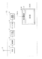
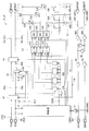
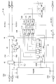
- FIG. 11 is a block diagram illustrating a configuration example of a display device according to an embodiment of the present disclosure.
- FIG. 3 is an explanatory diagram illustrating a configuration example of the display panel illustrated in FIG. 1. It is explanatory drawing showing the example of 1 structure of a data signal.
- FIG. 3 is a block diagram illustrating a configuration example of a pixel illustrated in FIG. 2.
- FIG. 3 is a state transition diagram illustrating an operation example of the control unit illustrated in FIG. 2.
- FIG. 3 is an explanatory diagram illustrating an operation example of each pixel illustrated in FIG. 2. It is explanatory drawing showing the example of a signal input into the pixel of the first rank. It is explanatory drawing showing the example of 1 operation
- FIG. 10 is another explanatory diagram illustrating an operation example in each pixel.
- FIG. 10 is another explanatory diagram illustrating an operation example in each pixel.
- FIG. 10 is another explanatory diagram illustrating an operation example in each pixel.
- FIG. 10 is another explanatory diagram illustrating an operation example in each pixel.
- FIG. 10 is another explanatory diagram illustrating an operation example in each pixel.
- FIG. 10 is another explanatory diagram illustrating an operation example in each pixel.
- FIG. 10 is another explanatory diagram illustrating an operation example in each pixel.
- FIG. 10 is another explanatory diagram illustrating an operation example in each pixel.
- FIG. 10 is another explanatory diagram illustrating an operation example in each pixel.
- FIG. 10 is another explanatory diagram illustrating an operation example in each pixel.
- FIG. 10 is another explanatory diagram illustrating an operation example in each pixel.
- FIG. 10 is another explanatory diagram illustrating an operation example in each pixel.
- FIG. 10 is another explanatory diagram illustrating an operation example in each pixel.
- FIG. 10 is another explanatory diagram illustrating an operation example in each pixel.
- FIG. 10 is another explanatory diagram illustrating an operation example in each pixel.
- FIG. 10 is another explanatory diagram illustrating an operation example in each pixel.
- FIG. 10 is another explanatory diagram illustrating an operation example in each pixel.
- FIG. 10 is another explanatory diagram illustrating an operation example in each pixel.
- FIG. 10 is another explanatory diagram illustrating an operation example in each pixel.
- FIG. 10 is another explanatory diagram illustrating an operation example in each pixel.
- FIG. 10 is another explanatory diagram illustrating an operation example in each pixel.
- FIG. 10 is another explanatory diagram illustrating an operation example in each pixel.
- FIG. 10 is another explanatory diagram illustrating an operation example in each pixel.
- FIG. 10 is another explanatory diagram illustrating an operation example in each pixel.
- FIG. 10 is another explanatory diagram illustrating an operation example in each pixel.
- FIG. 10 is another explanatory diagram illustrating an operation example in each pixel.
- FIG. 10 is another explanatory diagram illustrating an operation example in each pixel.
- FIG. 10 is another explanatory diagram illustrating an operation example in each pixel. It is a block diagram showing the example of 1 composition of the pixel concerning the modification of a 1st embodiment. It is a block diagram showing the example of 1 structure of the pixel which concerns on the other modification of 1st Embodiment. It is a block diagram showing the example of 1 structure of the pixel which concerns on the other modification of 1st Embodiment.
- FIG. 36 is an explanatory diagram for describing an operation of the pixel illustrated in FIG. 35.
- FIG. 35 is an explanatory diagram for describing an operation of the pixel illustrated in FIG. 35.
- FIG. 37 is an explanatory diagram illustrating an operation example of each pixel illustrated in FIG. 36. It is a block diagram showing the example of 1 structure of the pixel which concerns on the other modification of 1st Embodiment. It is a block diagram showing the example of 1 structure of the pixel which concerns on the other modification of 1st Embodiment. It is a block diagram showing the example of 1 structure of the memory part which concerns on the other modification of 1st Embodiment. It is explanatory drawing showing the example of 1 structure of the display panel which concerns on the other modification of 1st Embodiment. It is explanatory drawing showing the example of 1 structure of the display panel which concerns on the other modification of 1st Embodiment. It is explanatory drawing showing the example of 1 structure of the display panel which concerns on the other modification of 1st Embodiment.
- FIG. 10 is another explanatory diagram illustrating an operation example in each pixel. It is a block diagram showing the example of 1 structure of the pixel which concerns on a modification. It is a block diagram showing the example of 1 structure of the pixel which concerns on a modification. It is a block diagram showing the example of 1 structure of the pixel which concerns on a modification.
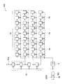
- FIG. 1 illustrates a configuration example of a display device according to the first embodiment.
- the display device 1 is a television device having an active matrix display panel using LEDs (Light Emitting Diodes) as display elements. Note that the display panel and the pixel chip according to the embodiment of the present disclosure are embodied by the present embodiment and will be described together.
- the display device 1 includes an RF (Radio Frequency) unit 11, a demodulation unit 12, a demultiplexer unit 13, a decoder unit 14, a signal conversion unit 15, and a display panel 20.
- RF Radio Frequency
- the RF unit 11 performs processing such as down-conversion on the broadcast wave (RF signal) received by the antenna 9.
- the demodulator 12 demodulates the signal supplied from the RF unit 11.
- the demultiplexer unit 13 separates these signals from the video signal and the audio signal multiplexed in the signal (stream) supplied from the demodulator 12.
- the decoder unit 14 decodes the signals (video signal and audio signal) supplied from the demultiplexer unit 13.
- the signal supplied from the demultiplexer unit 13 is a signal encoded by MPEG2 (Moving Picture Experts Group phase 2), and the decoder unit 14 performs a decoding process on this signal. To do.
- MPEG2 Motion Picture Experts Group phase 2
- the signal conversion unit 15 performs signal format conversion. Specifically, in this example, the signal supplied from the decoder unit 14 is a YUV format signal, and the signal conversion unit 15 converts the format of this signal to the RGB format. The signal conversion unit 15 outputs the signal whose format has been converted in this way as a video signal Sdisp.
- the display panel 20 is an active matrix display panel using LEDs as display elements.
- the display panel 20 includes a display driving unit 21 and a display unit 30.
- the display drive unit 21 controls light emission at each pixel Pix (described later) of the display unit 30 based on the video signal Sdisp supplied from the signal conversion unit 15. Specifically, as will be described later, the display drive unit 21 supplies the data signals PS and PD and the clock signal CK to each column of the pixels Pix of the display unit 30 to emit light from each pixel Pix. It comes to control.
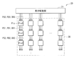
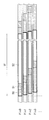
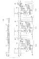
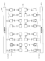
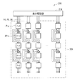
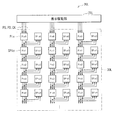
- FIG. 2 shows a configuration example of the display unit 30.
- the display unit 30 has a plurality of pixels Pix arranged in a matrix. Specifically, in this example, M pixels Pix are arranged in the horizontal direction (lateral direction) and N pixels in the vertical direction (vertical direction).
- the pixels Pix (Pix0, Pix1, Pix2,..., Pix (N ⁇ 1)) arranged in parallel in the vertical direction are connected in a daisy chain.
- the display driver 21 supplies the data signals PS, PD (PS0, PD0) and the clock signal CK (CK0) to the first stage pixel Pix0 in the pixels Pix for one column connected in a daisy chain.
- the pixel Pix0 generates data signals PS, PD (PS1, PD1) and a clock signal CK (CK1) based on the data signals PS0 and PD0 and the clock signal CK0, and supplies them to the pixel Pix1 at the next stage.
- the pixel Pix1 at the next stage generates data signals PS, PD (PS2, PD2) and a clock signal CK (CK2) based on the data signals PS1 and PD1 and the clock signal CK1, and supplies it to the next pixel Pix2. Supply.
- the final pixel Pix (N ⁇ 1) includes the data signals PS and PD (PS (N ⁇ 1) and PD (N ⁇ 1)) generated by the previous pixel Pix (N ⁇ 2) and the clock signal CK. (CK (N-1)) is received. In this way, the pixels Pix are daisy chained for the data signals PS and PD, and also daisy chained for the clock signal CK.
- FIG. 3 shows a configuration example of the data signals PS and PD.
- FIG. 3 shows data signals PS and PD related to one pixel Pix. That is, the display drive unit 21 supplies data signals PS and PD in which N signals shown in FIG. 3 are connected to N pixels Pix connected in a daisy chain.
- the data signal PD related to one pixel Pix is also referred to as a pixel packet PCT.
- the data signal PD has a flag RST, a flag PL, and a luminance data ID.
- the flag RST indicates the first pixel packet in each frame, as will be described later. Specifically, the flag RST becomes “1” in the first pixel packet PCT in each frame and becomes “0” in the other pixel packet PCT in the frame.
- the flag PL indicates whether or not the luminance data ID in the pixel packet PCT has already been read by any pixel Pix. Specifically, the flag PL is “0” when the luminance data ID has not been read yet, and “1” when the luminance data ID has already been read.
- the luminance data ID defines the light emission luminance in each pixel Pix.
- the luminance data ID includes luminance data IDR indicating red (R) emission luminance, luminance data IDG indicating green (G) emission luminance, and luminance data IDB indicating blue (B) emission luminance. Yes.
- the luminance data IDR, IDG, and IDB are codes each consisting of 12 bits.
- the data signal PS is “1” when the data signal PD indicates the flag RST, and “0” otherwise.
- the data signal PS is a signal that becomes “1” only at the start of each pixel packet PCT.
- Each pixel Pix receives the data signals PS and PD and the clock signal CK from the previous pixel Pix and supplies them to the next pixel Pix.
- Each pixel Pix reads luminance data ID related to the pixel Pix from the data signal PD, and emits light with light emission luminance corresponding to the luminance data ID.
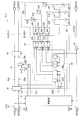
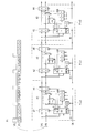
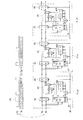
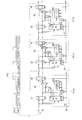
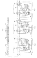
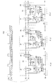
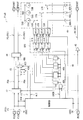
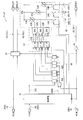
- FIG. 4 shows a configuration example of the pixel Pix.
- the pixel Pix includes a control unit 41, flip-flops 42 and 44, a selector unit 43, a buffer 45, a memory unit 46, a drive unit 50, and a light emitting unit 48.
- control unit 41 flip-flops 42 and 44
- selector unit 43 flip-flops 42 and 44
- buffer 45 buffer 45
- memory unit 46 memory unit 46
- drive unit 50 a light emitting unit 48.
- the pixel Pix0 includes data signals PS1, PD1, and a clock signal based on the data signal PS0 input to the input terminal PSIN, the data signal PD0 input to the input terminal PDIN, and the clock signal CK0 input to the input terminal CKIN.
- CK1 is generated.
- the pixel Pix0 outputs the data signal PS1 from the output terminal PSOUT, the data signal PD1 from the output terminal PDOUT, and the clock signal CK1 from the output terminal CKOUT.
- the control unit 41 is a state machine that sets the state of the pixel Pix0 based on the data signals PS0 and PD0 and the clock signal CK0 and generates signals LD, PLT, and CKEN.
- the signal LD and the signal PLT are signals for rewriting the flag PL included in the data signal PD, as will be described later.
- the signal LD is a signal that becomes the flag PL by this rewriting
- the signal PLT is a control signal that instructs the rewriting timing.
- the signal CKEN is a control signal for instructing the timing for storing the luminance data ID in the memory unit 46, as will be described later.
- the control unit 41 also has a function of supplying a control signal to the drive unit 50.
- the flip-flop 42 samples the data signal PS0 based on the clock signal CK0, outputs the result as the data signal PSA, samples the data signal PD0 based on the clock signal CK0, and outputs the result as the data signal PDA. To do.
- the flip-flop 42 is configured using, for example, a D-type flip-flop circuit for sampling the data signal PS0 and a D-type flip-flop circuit for sampling the data signal PD0.
- the selector unit 43 generates the data signal PDB based on the data signal PDA and the signals LD and PLT.
- the selector unit 43 includes selectors 43A and 43B. “0” is input to the first input terminal of the selector 43A, “1” is input to the second input terminal, and the signal LD is input to the control input terminal.
- the selector 43A outputs “0” input to the first input terminal when the signal LD is “0”, and “1” input to the second input terminal when the signal LD is “1”. "Is output.
- the data signal PDA is input to the first input terminal of the selector 43B, the output signal from the selector 43A is input to the second input terminal, and the signal PLT is input to the control input terminal.
- the selector 43B outputs the data signal PDA input to the first input terminal when the signal PLT is “0”, and the selector input to the second input terminal when the signal PLT is “1”.
- the output signal from 43A is output.
- the selector unit 43 supplies the output signal of the selector 43B to the flip-flop 44 as the data signal PDB.
- the selector unit 43 outputs the data signal PDA as it is as the data signal PDB during the period when the signal PLT is “0”, and the signal LD as the data signal PDB during the period when the signal PLT is “1”. Output as.
- the signal PLT is a signal in which the data signal PDA becomes “1” in the period indicating the flag PL and becomes “0” in the other periods. That is, the selector unit 43 generates the data signal PDB by replacing the flag PL in the data signal PDA with the signal LD.
- the flip-flop 44 samples the data signal PSA based on the clock signal CK0, outputs the result as the data signal PS1, samples the data signal PDB based on the clock signal CK0, and outputs the result as the data signal PD1. To do.
- the flip-flop 44 is configured by using two D-type flip-flop circuits, for example, like the flip-flop 42.
- the buffer 45 performs waveform shaping on the clock signal CK0 and outputs it as the clock signal CK1.
- the memory unit 46 stores the luminance data ID.
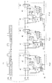
- the memory unit 46 includes an AND circuit 46A and a shift register 46B.
- the AND circuit 46A calculates a logical product of the signal at the first input terminal and the signal at the second input terminal.
- the signal CKEN supplied from the control unit 41 is input to the first input terminal of the AND circuit 46A, and the clock signal CK0 is input to the second input terminal.
- the shift register 46B is a 36-bit shift register in this example.
- the data signal PDA is input to the data input terminal of the shift register 46B, and the output signal of the AND circuit 46A is input to the clock input terminal.
- the memory unit 46 stores data included in the data signal PDA in a period in which the signal CKEN is “1”.
- the signal CKEN is a signal that the data signal PDA becomes “1” in the period indicating the pixel data ID for 36 bits related to the pixel Pix0 and becomes “0” in the other periods.
- the AND circuit 46A supplies the clock signal to the shift register 46B during the period in which the data signal PDA indicates the pixel data ID related to the pixel Pix0. In this way, the shift register 46B stores the 36-bit pixel data ID related to the pixel Pix0.
- the 12-bit portion from the last stage of the shift register 46B stores the luminance data IDR
- the 12-bit portion near the center stores the luminance data IDG
- the 12-bit portion from the first stage stores the luminance data IDB. Is to be remembered.
- the driving unit 50 drives the light emitting unit 48 based on the luminance data ID stored in the memory unit 46.
- the drive unit 50 includes registers 51R, 51G, and 51B, DACs (D / A converters) 52R, 52G, and 52B, and variable current sources 53R, 53G, and 53B.
- the registers 51R, 51G, and 51B store 12-bit data based on the control signal supplied from the control unit 41, respectively. Specifically, the register 51R stores the luminance data IDR stored in the 12-bit portion from the last stage of the shift register 46B, and the register 51G stores the luminance data stored in the 12-bit portion near the center. IDG is stored, and the register 51B stores the luminance data IDB stored in the 12-bit portion from the first stage.
- the DACs 52R, 52G, and 52B convert the 12-bit digital signals stored in the registers 51R, 51G, and 51B into analog signals based on the control signal supplied from the control unit 41, respectively.
- variable current sources 53R, 53G, and 53B generate drive currents corresponding to the analog signals supplied from the DACs 52R, 52G, and 52B, respectively.
- the light emitting unit 48 emits light based on the driving current supplied from the driving unit 50.
- the light emitting unit 48 includes light emitting elements 48R, 48G, and 48B.
- the light emitting elements 48R, 48G, and 48B are light emitting elements configured using LEDs, and emit red (R), green (G), and blue (B) light, respectively.
- the DAC 52R generates an analog voltage based on the luminance data IDR stored in the register 51R.
- the variable current source 53R generates a drive current based on the analog voltage and supplies the drive current to the light emitting element 48R of the light emitting unit 48 via the switch 54R.
- the light emitting element 48R emits light with a light emission luminance corresponding to the driving current.
- the DAC 52G generates an analog voltage based on the luminance data IDG stored in the register 51G
- the variable current source 53G generates a drive current based on the analog voltage, and the light emitting unit via the switch 54G.
- the light emitting element 48G emits light with light emission luminance corresponding to the driving current.
- the DAC 52B generates an analog voltage based on the luminance data IDB stored in the register 51B, and the variable current source 53B generates a drive current based on the analog voltage, and the light emitting unit 48 via the switch 54B.
- the light emitting element 48B emits light with light emission luminance corresponding to the driving current.
- switches 54R, 54G, and 54B are configured to be turned on / off by a control signal supplied from the control unit 41, whereby red (R), green (G), The light emission luminance can be adjusted while maintaining the balance of each blue (B) light emission luminance.
- each block excluding the light emitting section 48 is integrated on one chip.
- (M ⁇ N) chips and (M ⁇ N) light emitting units 48 are arranged in a matrix on the display panel 20.
- the pixel Pix corresponds to a specific example of “first unit pixel” in the present disclosure.
- the input terminal PDIN corresponds to a specific example of “first data input terminal” in the present disclosure
- the output terminal PDOUT corresponds to a specific example of “first data output terminal” in the present disclosure.
- the data signal PD corresponds to a specific example of “first data” in the present disclosure.
- the flip-flops 42 and 44 correspond to a specific example of “first waveform shaping unit” in the present disclosure.
- the input terminal PSIN corresponds to a specific example of “second data input terminal” in the present disclosure
- the output terminal PSOUT corresponds to a specific example of “second data output terminal” in the present disclosure.
- the data signal PS corresponds to a specific example of “second data” in the present disclosure.
- the flip-flops 42 and 44 correspond to a specific example of “second waveform shaping unit” in the present disclosure.
- the input terminal CKIN corresponds to a specific example of “first clock input terminal” in the present disclosure
- the output terminal CKOUT corresponds to a specific example of “first clock output terminal” in the present disclosure.
- the buffer 45 corresponds to a specific example of “first buffer” in the present disclosure.
- the light emitting elements 48R, 48G, and 48B correspond to a specific example of “display element” in the present disclosure.
- the DACs 52R, 52G, and 52B correspond to a specific example of “conversion unit” in the present disclosure.
- the RF unit 11 performs processing such as down-conversion on the broadcast wave (RF signal) received by the antenna 19.
- the demodulation unit 12 performs demodulation processing on the signal supplied from the RF unit 11.
- the demultiplexer unit 13 separates these signals from the video signal and audio signal multiplexed in the signal (stream) supplied from the demodulator 12.
- the decoder unit 14 decodes the signals (video signal and audio signal) supplied from the demultiplexer unit 13.
- the signal converter 15 converts the format of the signal and outputs it as a video signal Sdisp.
- the display driving unit 21 controls light emission in each pixel Pix of the display unit 30 based on the video signal Sdisp supplied from the signal conversion unit 15. Specifically, the display driving unit 21 supplies the data signals PS and PD and the clock signal CK to each column of the pixels Pix in the display unit 30. Each pixel Pix receives the data signals PS and PD and the clock signal CK from the previous pixel Pix and supplies them to the next pixel Pix. Each pixel Pix reads luminance data ID related to the pixel Pix from the data signal PD, and emits light with light emission luminance corresponding to the luminance data ID.
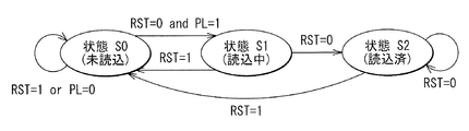
- control unit 41 functions as a state machine and controls the operation of the pixel Pix. First, the operation of the control unit 41 will be described in detail.
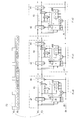
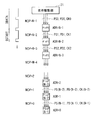
- FIG. 5 shows a state transition diagram of the control unit 41. As shown in FIG. 5, the pixel Pix has three states S0 to S2.
- State S0 indicates a state in which the pixel Pix has not read the luminance data ID (Unloaded).
- the control unit 41 sets the signal LD to “0”. Thereby, the pixel Pix replaces the flag PL in the input signal PD with “0”. Further, the control unit 41 sets CKEN to “0”.
- State S1 indicates a state in which the pixel Pix is reading the luminance data ID (Loading).
- the control unit 41 sets the signal LD to “0”.
- the pixel Pix replaces the flag PL in the input signal PD with “0”.
- the control unit 41 sets the signal CKEN to “1” during the period when the signal PDA indicates the luminance data ID, and sets the signal CKEN to “0” during the other periods.
- the luminance data ID is stored in the memory unit 46.
- State S2 indicates a state in which the pixel Pix has read the luminance data ID (Loaded).
- the control unit 41 sets the signal LD to “1”. Thereby, the pixel Pix replaces the flag PL in the input signal PD with “1”. Further, the control unit 41 sets CKEN to “0”.
- the transition between these three states S0 to S2 is performed based on the flags RST and PL included in the data signal PD.
- the control unit 41 sets the pixel Pix to the state S0 (unread).
- this state S0 unread
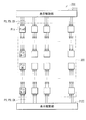
- FIG. 6 shows the states of the pixels Pix0 to Pix (N ⁇ 1) in one frame period (1F).
- “1” is input as the flag RST to the first-stage pixel Pix0, and the state of the pixel Pix0 is set to the state S0 (unread).
- the pixels Pix1 to Pix (N-1) are sequentially set to the state S0 (unread) within the one frame period (1F).
- the start timing of the period S0 (unread) in the adjacent pixel Pix is shifted by two pulses of the clock signal CK, as will be described later.
- the states of the pixels Pix0 to Pix (N-1) sequentially transition from the state S0 (unread) to the state S1 (reading).
- the period of the state S1 (reading) in the adjacent pixels Pix is set so as not to overlap each other.
- each pixel Pix0 to Pix (N-1) sequentially reads the luminance data ID.
- the state of each pixel Pix0 to Pix (N ⁇ 1) sequentially transitions from the state S1 (reading) to the state S2 (reading).
- each of the pixels Pix0 to Pix (N-1) emits light with a luminance corresponding to the read luminance data ID.
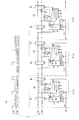
- FIG. 7 shows an example of a signal input to a column of pixels Pix connected in a daisy chain in one frame period (1F), (A) shows the waveform of the clock signal CK, (B) The waveform of the data signal PS is shown, (C) shows the data of the data signal PD.
- “x” indicates that either “1” or “0” may be used.
- the luminance data IDR, IDG, and IDB are 1-bit data
- “r0”, “r1”,..., “R (N ⁇ 1)” indicate the luminance data IDR.
- “G0”, “g1”,..., “G (N ⁇ 1)” indicate luminance data IDG
- “b0”, “b1”,..., “B (N ⁇ 1)” indicate luminance data IDB. .
- the flag RST is “1” in the first pixel packet PCT in one frame period (1F), and “0” in the other pixel packets PCT.
- the flag PL is “1” in the second and subsequent pixel packets PCT in one frame period (1F).
- the flip-flop 42 of the pixel Pix0 samples the input data signals PS and PD as shown in FIG.
- the control unit 41 of the pixel Pix0 acquires the value “1” of the flag RST from the signal portion P1, and sets the state of the pixel Pix0 to the state S0 (unread). That is, the control unit 41 sets the signals LD, PLT, and CKEN to “0”.
- the flip-flops 42 and 44 sample the input data signals, respectively.
- the control unit 41 of the pixel Pix0 sets the signal PLT to “1”.
- the selector unit 43 outputs “0”, which is the same as the signal LD. That is, the selector unit 43 replaces the flag PL (“x”) with “0” of the signal LD.
- the control unit 41 returns the signal PLT to “0”. Thereby, the selector unit 43 selects and outputs the data signal PDA from the flip-flop 42.
- the control unit 41 acquires the value “1” of the flag RST from the signal portion P1, and sets the state of the pixel Pix1 to the state S0 (unread). That is, the control unit 41 sets the signals LD, PLT, and CKEN to “0”.
- the flip-flops 42 and 44 sample the input data signal.
- the signal portion P2 is input to the pixel Pix1 at the next stage.
- the control unit 41 sets the signal PLT to “1”.
- the selector unit 43 outputs “0”, which is the same as the signal LD.
- the control unit 41 returns the signal PLT to “0”. Thereby, the selector unit 43 selects and outputs the data signal PDA from the flip-flop 42.
- the control unit 41 acquires the value “1” of the flag RST from the signal portion P1, and sets the state of the pixel Pix2 to the state S0 (unread). That is, the control unit 41 sets the signals LD, PLT, and CKEN to “0”.
- the flip-flops 42 and 44 respectively sample the input data signal.
- the signal portion P4 is input to the pixel Pix1
- the signal portion P2 is input to the pixel Pix2.
- control unit 41 acquires the value “0” of the flag RST from the signal portion P6.
- the control unit 41 sets the signal PLT to “1”. As a result, the selector unit 43 outputs “0”, which is the same as the signal LD.
- the control unit 41 acquires the value “1” of the flag PL from the signal portion P7. Since the control unit 41 has acquired the value “0” of the flag RST at the immediately preceding timing, the control unit 41 sets the state of the pixel Pix1 to state S1 (reading). Further, the control unit 41 sets the signal PLT to “1”. As a result, the selector unit 43 outputs “0”, which is the same as the signal LD. That is, the selector unit 43 replaces the flag PL (“1”) with the signal LD “0”.
- the control unit 41 returns the signal PLT to “0”. Thereby, the selector unit 43 selects and outputs the data signal PDA from the flip-flop 42.
- the flip-flops 42 and 44 sample the input data signals, respectively. Thereby, the signal portion P6 is input to the pixel Pix1, and the signal portion P4 is input to the pixel Pix2.
- the control unit 41 In the pixel Pix0, the control unit 41 returns the signal PLT to “0”. Thereby, the selector unit 43 selects and outputs the data signal PDA from the flip-flop 42. Further, the control unit 41 sets the signal CKEN to “1”.
- control unit 41 acquires the value “0” of the flag RST from the signal portion P6.
- the flip-flops 42 and 44 sample the input data signals. Thereby, the signal portion P7 is input to the pixel Pix1, and the signal portion P5 is input to the pixel Pix2.
- the shift register 46B stores the value “r0” of the luminance data IDR.
- the control unit 41 acquires the value “0” of the flag PL from the signal portion P7. Therefore, the state of the pixel Pix1 is maintained in the state S0 (unread). Further, the control unit 41 sets the signal PLT to “1”. As a result, the selector unit 43 outputs “0”, which is the same as the signal LD.
- the shift register 46B stores the value “g0” of the luminance data IDG.
- the control unit 41 returns the signal PLT to “0”. Thereby, the selector unit 43 selects and outputs the data signal PDA from the flip-flop 42.
- control unit 41 acquires the value “0” of the flag RST from the signal portion P6.
- the flip-flops 42 and 44 sample the input data signals.
- the signal portion P9 is input to the pixel Pix1
- the signal portion P7 is input to the pixel Pix2.
- the shift register 46B stores the value “b0” of the luminance data IDB.
- the shift register 46B (memory unit 46) stores all the luminance data IDR, IDG, IDB related to the pixel Pix0.
- the control unit 41 acquires the value “0” of the flag RST from the signal portion P11, and sets the state of the pixel Pix0 to the state S2 (read). That is, the control unit 41 sets the signal LD to “1”.
- the control unit 41 acquires the value “0” of the flag PL from the signal portion P7. Therefore, the state of the pixel Pix1 is maintained in the state S0 (unread). Further, the control unit 41 sets the signal PLT to “1”. As a result, the selector unit 43 outputs “0”, which is the same as the signal LD.
- the flip-flops 42 and 44 sample the input data signal. Thereby, the signal portion P10 is input to the pixel Pix1, and the signal portion P8 is input to the pixel Pix2.
- the control unit 41 sets the signal PLT to “1”. Thereby, the selector unit 43 outputs “1” which is the same as the signal LD.
- the control unit 41 returns the signal PLT to “0”. Thereby, the selector unit 43 selects and outputs the data signal PDA from the flip-flop 42.
- the flip-flops 42 and 44 sample the input data signals.
- the signal portion P11 is input to the pixel Pix1
- the signal portion P9 is input to the pixel Pix2.
- the control unit 41 returns the signal PLT to “0”. Thereby, the selector unit 43 selects and outputs the data signal PDA from the flip-flop 42.
- control unit 41 acquires the value “0” of the flag RST from the signal portion P11.
- the flip-flops 42 and 44 sample the input data signals. Thereby, the signal portion P12 is input to the pixel Pix1, and the signal portion P10 is input to the pixel Pix2.
- the control unit 41 acquires the value “1” of the flag PL from the signal portion P12. Since the control unit 41 has acquired the value “0” of the flag RST at the immediately preceding timing, the control unit 41 sets the state of the pixel Pix1 to state S1 (reading). Further, the control unit 41 sets the signal PLT to “1”. As a result, the selector unit 43 outputs “0”, which is the same as the signal LD. That is, the selector unit 43 replaces the flag PL (“1”) with the signal LD “0”.
- the flip-flops 42 and 44 respectively sample the input data signal.
- the signal portion P13 is input to the pixel Pix1
- the signal portion P11 is input to the pixel Pix2.
- the control unit 41 returns the signal PLT to “0”. Thereby, the selector unit 43 selects and outputs the data signal PDA from the flip-flop 42. Further, the control unit 41 sets the signal CKEN to “1”.
- control unit 41 acquires the value “0” of the flag RST from the signal portion P11.
- the flip-flops 42 and 44 sample the input data signal in each pixel Pix, as shown in FIG. Thereby, the signal portion P14 is input to the pixel Pix1, and the signal portion P12 is input to the pixel Pix2.
- the control unit 41 acquires the value “0” of the flag RST from the signal portion P16. Therefore, the state of the pixel Pix0 is maintained in the state S2 (read).
- the shift register 46B stores the value “r1” of the luminance data IDR.
- the control unit 41 acquires the value “0” of the flag PL from the signal portion P12. Therefore, the state of the pixel Pix2 is maintained in the state S0 (unread). Further, the control unit 41 sets the signal PLT to “1”. As a result, the selector unit 43 outputs “0”, which is the same as the signal LD.
- the flip-flops 42 and 44 sample the input data signals, respectively. Thereby, the signal portion P15 is input to the pixel Pix1, and the signal portion P13 is input to the pixel Pix2.
- the control unit 41 sets the signal PLT to “1”. Thereby, the selector unit 43 outputs “1” which is the same as the signal LD.
- the shift register 46B stores the value “g1” of the luminance data IDG.
- the control unit 41 returns the signal PLT to “0”. Thereby, the selector unit 43 selects and outputs the data signal PDA from the flip-flop 42.
- the flip-flops 42 and 44 sample the input data signal in each pixel Pix.
- the signal portion P16 is input to the pixel Pix1
- the signal portion P14 is input to the pixel Pix2.
- the control unit 41 returns the signal PLT to “0”. Thereby, the selector unit 43 selects and outputs the data signal PDA from the flip-flop 42.
- the shift register 46B stores the value “b1” of the luminance data IDB.
- the shift register 46B (memory unit 46) stores all the luminance data IDR, IDG, IDB related to the pixel Pix1.
- the control unit 41 acquires the value “0” of the flag RST from the signal portion P18, and sets the state of the pixel Pix0 to the state S2 (read). That is, the control unit 41 sets the signal LD to “1”.
- the control unit 41 sets the signal PLT to “1”. Thereby, the selector unit 43 outputs “1” which is the same as the signal LD.
- the flip-flops 42 and 44 respectively sample the input data signal.
- the signal portion P18 is input to the pixel Pix1
- the signal portion P16 is input to the pixel Pix2.
- the control unit 41 returns the signal PLT to “0”. Thereby, the selector unit 43 selects and outputs the data signal PDA from the flip-flop 42.
- control unit 41 acquires the value “0” of the flag RST from the signal portion P16.
- the flip-flops 42 and 44 sample the input data signals in each pixel Pix. Thereby, the signal portion P19 is input to the pixel Pix1, and the signal portion P17 is input to the pixel Pix2.
- the control unit 41 acquires the value “0” of the flag RST from the signal portion P21. Therefore, the state of the pixel Pix0 is maintained in the state S2 (read).
- the control unit 41 acquires the value “1” of the flag PL from the signal portion P17. Since the control unit 41 has acquired the value “0” of the flag RST at the immediately preceding timing, the control unit 41 sets the state of the pixel Pix2 to the state S1 (reading). Further, the control unit 41 sets the signal PLT to “1”. As a result, the selector unit 43 outputs “0”, which is the same as the signal LD. That is, the selector unit 43 replaces the flag PL (“1”) with the signal LD “0”.
- the flip-flops 42 and 44 sample the input data signals in the respective pixels Pix.
- the signal portion P20 is input to the pixel Pix1
- the signal portion P18 is input to the pixel Pix2.
- the control unit 41 sets the signal PLT to “1”. Thereby, the selector unit 43 outputs “1” which is the same as the signal LD.
- the control unit 41 returns the signal PLT to “0”. Thereby, the selector unit 43 selects and outputs the data signal PDA from the flip-flop 42. Further, the control unit 41 sets the signal CKEN to “1”.
- the flip-flops 42 and 44 sample the input data signals. Thereby, the signal portion P21 is input to the pixel Pix1, and the signal portion P19 is input to the pixel Pix2.
- the control unit 41 returns the signal PLT to “0”. Thereby, the selector unit 43 selects and outputs the data signal PDA from the flip-flop 42.
- the control unit 41 acquires the value “0” of the flag RST from the signal portion P21. Therefore, the state of the pixel Pix0 is maintained in the state S2 (read).
- the shift register 46B stores the value “r2” of the luminance data IDR.
- the flip-flops 42 and 44 sample the input data signals, respectively.
- the signal portion P22 is input to the pixel Pix1
- the signal portion P20 is input to the pixel Pix2.
- the control unit 41 sets the signal PLT to “1”. Thereby, the selector unit 43 outputs “1” which is the same as the signal LD.
- the shift register 46B stores the value “g2” of the luminance data IDG.
- the flip-flops 42 and 44 respectively sample the input data signal.
- the signal portion P23 is input to the pixel Pix1
- the signal portion P21 is input to the pixel Pix2.
- the control unit 41 returns the signal PLT to “0”. Thereby, the selector unit 43 selects and outputs the data signal PDA from the flip-flop 42.
- the shift register 46B stores the value “b2” of the luminance data IDB.
- the shift register 46B (memory unit 46) stores all the luminance data IDR, IDG, IDB related to the pixel Pix2.
- the control unit 41 acquires the value “0” of the flag RST from the signal portion P21, and sets the state of the pixel Pix0 to the state S2 (read). That is, the control unit 41 sets the signal LD to “1”.
- each pixel Pix receives the data signals PS and PD and the clock signal CK from the previous pixel Pix and supplies them to the next pixel Pix.
- Each pixel Pix reads luminance data ID related to the pixel Pix from the data signal PD, and emits light with light emission luminance corresponding to the luminance data ID.
- the drive unit drives each pixel via a gate line or a data line.
- These gate lines and data lines are so-called global wirings connected to a plurality of pixels for one column or a plurality of pixels for one row.
- these wirings become long, so that the resistance and parasitic capacitance of the wirings increase, and each pixel may not be driven sufficiently. .
- the time allocated to one horizontal period (1H) is shortened, and each pixel May not be able to be driven sufficiently.
- the time allocated to one horizontal period (1H) is shortened, and there is a possibility that each pixel cannot be driven sufficiently.
- the pixels Pix are daisy chain connected. That is, each pixel Pix drives the next pixel Pix not through the global wiring as described above but through a local wiring between the pixels Pix. Therefore, each pixel Pix can drive the next pixel Pix relatively easily through such a short wiring, and a large-screen display device can be realized. Further, since each pixel Pix has a short wiring, the transfer speed of the data signals PS and PD can be increased relatively easily, and a high-definition display device and a display device with a high frame rate can be realized.
- the configuration of the display device 1 can be simplified. That is, for example, in the display device described in Patent Document 1, a plurality of gate lines extending in the horizontal direction (lateral direction), a plurality of data lines extending in the vertical direction (longitudinal direction), and so-called connected to the gate lines. Since a gate driver and a so-called data driver connected to the data line are provided, the configuration may be complicated. On the other hand, in the display device 1 according to the present embodiment, since the pixels Pix are daisy-chain connected, only wiring extending in the vertical direction (longitudinal direction) needs to be provided as shown in FIG. Further, it is not necessary to provide wiring extending in the horizontal direction (lateral direction) and a driving unit for driving the wiring, and the configuration of the display device 1 can be simplified.
- the influence of noise on the image quality can be reduced.
- the display device described in Patent Document 1 uses an analog signal, the image quality may deteriorate due to noise.
- the influence of noise on the image quality may be further increased.
- the display apparatus 1 according to the present embodiment uses digital signals, the influence of noise on the image quality can be reduced.
- the signal amplitude may increase from the viewpoints of gradation expression and noise resistance, and in this case, radiation increases.
- the signal amplitude can be reduced, so that radiation can be reduced.
- each pixel Pix has the flip-flops 42 and 44 and the buffer 45, so that the signal amplitude of the data signals PS and PD can be reduced. That is, for example, when the flip-flops 42 and 44 and the buffer 45 are not provided, the signal amplitude may be attenuated as the distance from the display driving unit increases. In this case, the display driving unit needs to generate data signals PS and PD having a large signal amplitude.
- the signal amplitude is maintained by shaping the waveform of the data signals PS and PD and the clock signal CK every time it passes through the pixel Pix.
- the signal amplitude of the data signals PS and PD can be reduced.
- the above-described radiation can be reduced, the power supply voltage can be lowered, and the power consumption can be reduced.
- the memory unit 46 is provided in each pixel Pix, for example, when displaying a still image, it is not necessary to perform data transfer, so that power consumption can be reduced.
- the flip-flops 42 and 44 that sample the data signals PS and PD based on the clock signal CK are provided in each pixel, the data signals PS and PD and the clock signal CK are provided between the data signals PS and PD. A relative phase relationship can be maintained.
- the pixels are daisy chained, so that, for example, a display device with a large screen, high definition, or a high frame rate can be realized, and image quality can be improved.
- the configuration of the display device can be simplified.
- each pixel has a flip-flop and a buffer, the signal amplitude can be reduced, radiation can be reduced, and power consumption can be reduced.
- each pixel is provided with a flip-flop that samples the data signal based on the clock signal, the relative phase relationship between the data signal and the clock signal can be maintained.
- the clock signal CK is supplied to each pixel Pix.
- the present invention is not limited to this.
- a differential clock signal may be supplied to each pixel.
- the present modification will be described in detail with some examples.
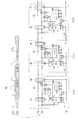
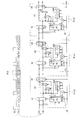
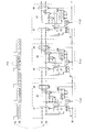
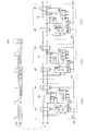
- FIG. 33 illustrates a configuration example of the pixel PixB according to the present modification.
- the pixel PixB includes buffers 61, 64, 65, 68, and 69 and inverters 66 and 67.
- description will be made using the first stage pixel PixB0 among the pixels PixB for one column connected in a daisy chain, but the same applies to the other pixels PixB1 to PixB (N ⁇ 1).
- the pixel PixB0 generates data signals PS1, PD1, and clock signals CKP1, CKN1 based on the data signals PS0, PD0, the clock signal CKP0 input to the input terminal CKPIN, and the clock signal CKN0 input to the input terminal CKNIN. To do.
- the pixel PixB0 outputs the data signal PS1 from the output terminal PSOUT, outputs the data signal PD1 from the output terminal PDOUT, outputs the clock signal CKP1 from the output terminal CKPOUT, and outputs the clock signal CKN1 from the output terminal CKNOUT. It has become.
- the clock signal CKP and the clock signal CKN are signals inverted from each other. That is, the pixel PixB0 according to this modification operates with the differential clock signals CKP and CKN.
- Buffer 61 is a circuit that converts a differential signal into a single-ended signal. Specifically, the buffer 61 converts the clock signals CKP0 and CKN0 that are differential signals into a clock signal CK that is a single-ended signal.
- Buffers 64 and 65 perform waveform shaping on the input signal and output it. Specifically, the buffer 64 performs waveform shaping on the clock signal CKP0, and the buffer 65 shapes the waveform on the clock signal CKN0.
- the inverters 66 and 67 are inverting circuits that invert the input signal and output it.
- the input terminal of the inverter 66 is connected to the output terminal of the inverter 67 and the output terminal of the buffer 65, and the output terminal of the inverter 66 is connected to the input terminal of the inverter 67 and the output terminal of the buffer 64.
- the input terminal of the inverter 67 is connected to the output terminal of the inverter 66 and the output terminal of the buffer 64, and the output terminal of the inverter 67 is connected to the input terminal of the inverter 66 and the output terminal of the buffer 65.
- the inverters 66 and 67 constitute a latch circuit.
- the buffer 68 performs waveform shaping on the output signal of the buffer 64 and outputs it as the clock signal CKP1.
- the buffer 69 performs waveform shaping on the output signal of the buffer 65 and outputs it as the clock signal CKN1.
- the input terminal CKPIN corresponds to a specific example of “first clock input terminal” in the present disclosure
- the output terminal CKPOUT corresponds to a specific example of “first clock output terminal” in the present disclosure.
- the clock signal CKP corresponds to a specific example of “first clock signal” in the present disclosure.
- the input terminal CKNIN corresponds to a specific example of “second clock input terminal” in the present disclosure
- the output terminal CKNOUT corresponds to a specific example of “second clock output terminal” in the present disclosure.
- the clock signal CKN corresponds to a specific example of “second clock signal” in the present disclosure.
- the differential clock signals CKP and CKN are used, it is possible to reduce the possibility that the waveform of the clock signal deteriorates due to transmission. That is, when the single-ended clock signal CK is used as in the above embodiment, for example, the duty ratio of the clock signal CK may change after passing through the plurality of buffers 45. . Such a phenomenon may occur, for example, when the transistors constituting the buffer 45 have characteristic variations. When the duty ratio changes in this way, for example, clock transmission cannot be performed normally, or the sampling timing in the flip-flop 42 of the pixel Pix may be shifted, and normal operation may not be performed. On the other hand, in the pixel PixB according to the present modification, the change in the duty ratio can be suppressed by using the differential clock signals CKP and CKN and the inverters 66 and 67 performing the latch operation.
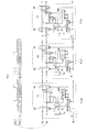
- This pixel PixC has inverters 68C and 69C.
- the input terminal of the inverter 68C is connected to the output terminal of the buffer 64, and the output terminal of the inverter 68C is connected to the output terminal CKNOUT.
- the input terminal of the inverter 69C is connected to the output terminal of the buffer 65, and the output terminal of the inverter 69C is connected to the output terminal CKPOUT. Note that the present invention is not limited to this configuration, and instead of this, for example, the inverters 66 and 67 in FIG. 34 may be omitted.
- the clock signal CKN1 is generated based on the clock signal CKP0, and the clock signal CKP1 is generated based on the clock signal CKN0.
- the influence of this asymmetry is corrected, and the clock signals CKP and CKN can be transmitted more reliably.
- the drive unit 50 is configured using the DACs 52R, 52G, and 52B.
- the drive unit 50 is not limited to this, and the drive unit may be configured using, for example, a counter. .
- the pixel PixD according to this modification will be described in detail.
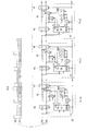
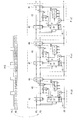
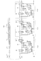
- FIG. 35 shows a configuration example of the pixel PixD.
- the pixel PixD includes a control unit 41D and a drive unit 50D.
- the control unit 41D has a function similar to that of the control unit 41 according to the above embodiment, functions as a state machine, and supplies a control signal to the drive unit 50D.
- the drive unit 50D includes counters 55R, 55G, and 55B, current sources 56R, 56G, and 56B, and switches 57R, 57G, and 57B.
- the counters 55R, 55G, and 55B count the clock pulses using the control signal (counter clock signal) supplied from the control unit 41D as a reference, thereby obtaining the luminance data IDR, stored in the registers 51R, 51G, and 51B.
- the counter generates pulse signals having pulse widths corresponding to IDG and IDB.
- the current sources 56R, 56G, and 56B generate constant drive currents, respectively.
- the switches 57R, 57G, 57B are turned on / off based on the pulse signals supplied from the counters 55R, 55G, 55B.
- the counter 55R generates a pulse signal having a pulse width corresponding to the luminance data IDR stored in the register 51R.
- the switch 57R is turned on / off based on this pulse signal, and supplies the drive current generated by the current source 57R to the light emitting element 48R.
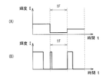
- FIG. 36A shows the operation of the pixel Pix according to the above embodiment
- FIG. 36B shows the operation of the pixel PixD according to this modification.
- the pixel Pix according to the above embodiment changes the light emission luminance (luminance ⁇ time) by changing the luminance I, but the pixel PixD according to the present modification changes the light emission time width.
- the light emission luminance (luminance ⁇ time) is changed.
- FIG. 37 shows the state of each pixel PixD0 to PixD (N-1) in one frame period (1F).
- the state of the first pixel PixD0 is set to the state S0 (unread).
- the pixels PixD1 to PixD (N ⁇ 1) are sequentially set to the state S0 (unread) within the one frame period (1F).
- the state of each pixel PixD0 to PixD (N-1) sequentially transitions from the state S0 (unread) to the state S1 (reading), and then further transitions to the state S2 (read).
- each pixel PixD0 to PixD (N-1) emits light for a period corresponding to the read luminance data ID. Then, after the period has elapsed, the pixels PixD0 to PixD (N ⁇ 1) are extinguished.
- the drive unit 50D is provided with the three counters 53R, 53G, and 53B.
- the present invention is not limited to this.
- the counter 50R is always based on one counter and the output signal of the counter.
- a pulse signal generation circuit that generates pulse signals having pulse widths corresponding to the luminance data IDR, IDG, and IDB may be provided.
- each pixel Pix receives the clock signal CK from the previous stage, generates a counter clock signal based on the clock signal CK, and supplies it to the counters 55R, 55G, and 55B.
- the present invention is not limited to this. Absent. Instead, for example, the display driver 21 generates a counter clock signal, each pixel Pix receives the counter clock signal from the previous stage, and supplies the counter clock signal to the counters 55R, 55G, and 55B. Also good.
- the frequency of the counter clock signal can be set independently of the frequency of the clock signal CK by daisy chaining the pixels Pix with respect to the counter clock signal, the light emitting elements 48R, 48G, and 48B emit light. The degree of freedom in setting the time can be further increased.
- the pixel Pix is provided with the three light emitting elements 48R, 48G, and 48B of red (R), green (G), and blue (B).
- the present invention is not limited to this. Instead, for example, four light emitting elements of red (R), green (G), blue (B), and white (W) may be provided.
- any one of red (R), green (G), and blue (B) light emitting elements may be provided in the pixel PixE.
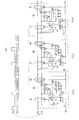
- the pixel PixE includes a memory unit 46E, a drive unit 50E, a light emitting element 49, and a control unit 41E.
- the drive unit 50E includes only one system among the three systems provided in the drive unit 50 according to the above embodiment.
- the number of bits in the memory unit 46E 1/3 of the number of bits in the memory 46 according to the above embodiment.
- the flip-flops 42 and 44 are provided in the pixel Pix.
- buffers 71 and 72 are provided as shown in FIG. Also good.
- the data signal PS0 is input to the input terminal of the buffer 71, and the data signal PS1 is output from the output terminal.
- the data signal PDB is input to the input terminal of the buffer 72, and the data signal PD1 is output from the output terminal.
- the present invention is not limited to such buffers 71 and 72, and any buffer that compensates the waveform may be used.
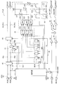
- the memory unit 46 is configured by using the 36-bit shift register 46B.
- the memory unit 46B includes a shift register 73, a frequency dividing circuit 74, and a shift register block 75.
- the shift register 73 is a 4-bit shift register, and the data signal PDA is input to the data input terminal, and the output signal of the AND circuit 46A is input to the clock input terminal.
- the frequency dividing circuit 74 divides the input signal by 1 ⁇ 4, and the output signal of the AND circuit 46A is input to the input terminal.
- the shift register block 75 has four 9-bit shift registers.
- luminance data ID (IDR, IDG, IDB) included in the data signal PDA is serial / parallel converted by the shift register 73 and stored in the shift register block 75.
- the luminance data IDR is stored in a portion PR near the final stage of the shift register block 75
- the luminance data IDG is stored in a portion PG near the center
- the luminance data IDB is stored in a portion PB near the first stage.
- each block excluding the light emitting portion 48 is integrated on one chip.
- the present invention is not limited to this.
- TFTs are formed on the substrate of the display panel 20. May be used.
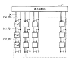
- N pixels Pix from the uppermost pixel Pix0 to the lowermost pixel Pix (N ⁇ 1) in the vertical direction are connected in a daisy chain, but the present invention is not limited to this.
- M pixels Pix from the first-stage pixel Pix0 to the pixel Pix (M ⁇ 1) are daisy-chain connected to display the display unit 30I.
- the display driver 211 provided on the upper side supplies the data signals PS and PD and the clock signal CK, and daisy-chains (NM) pixels Pix from the pixel Pix (M) to the pixel Pix (N-1).
- the display driving unit 212 provided in the lower part of the display unit 30I in a chain connection may supply the data signals PS and PD and the clock signal CK.
- the N pixels Pix connected in a daisy chain are arranged in a line in the vertical direction.
- the present invention is not limited to this, and for example, as shown in FIG. In this way, the display unit 30J may be arranged so as to be folded back near the center in the vertical direction.
- each pixel Pix connected in a daisy chain drives one pixel Pix.
- the present invention is not limited to this. Instead, for example, as shown in FIGS. A plurality (two in this example) of pixels Pix may be driven.
- each pixel Pix (for example, Pix0) connected in a daisy chain drives a subsequent pixel Pix (for example, Pix1) connected in a daisy chain and another pixel SPix (for example, SPix0).
- the series of pixels Pix and the series of pixels SPix are arranged in the same column.
- a series of pixels Pix and a series of pixels SPix are arranged in columns adjacent to each other.
- the data terminals PSOUT, PDOUT, and the clock CK may not be output by setting the output terminals PSOUT, PDOUT, and CKOUT to a high impedance state.
- the pixels Pix connected in a daisy chain are arranged in a line in the vertical direction.
- the present invention is not limited to this. Instead, for example, as shown in FIG. You may arrange in a line in the direction.
- an address ADR is assigned to N pixels PixP connected in a daisy chain, and each pixel PixP acquires a pixel data ID related to the pixel PixP based on the address ADR.
- symbol is attached
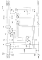
- the display device 2 includes a display panel 90 as shown in FIG.
- the display panel 90 includes a display unit 80 including N pixels PixP connected in a daisy chain.
- FIG. 46 shows a configuration example of the pixel PixP.
- the pixel PixP has a control unit 81 and a flip-flop 82.
- the description will be given using the first stage pixel PixP0 of the pixels PixP for one column connected in a daisy chain, but the same applies to the other pixels PixP1 to PixP (N ⁇ 1).
- the control unit 81 acquires and holds the address ADR of the pixel PixP0 based on the data signals PS0 and PD0 and the clock signal CK0, and generates the data signal PDC and the signal CKEN. Specifically, as described later, control unit 81 obtains address ADR based on data NOP included in partial DSTART of data signal PD0, and sets data NOP to a value obtained by subtracting 1 from the value. Instead, the data signal PDC is output. As will be described later, the control unit 81 generates a clock CKEN based on the address ADR and the data signal PS0, and acquires the luminance data ID related to the pixel PixP0 from the data signal PD0. The control unit 81 also has a function of supplying a control signal to the drive unit 50, similarly to the control unit 41 according to the first embodiment.
- the flip-flop 82 samples the data signal PS0 based on the clock signal CK0, outputs the result as the data signal PS1, samples the data signal PDC based on the clock signal CK0, and outputs the result as the data signal PD1. To do.
- the flip-flop 82 is configured using two D-type flip-flop circuits, for example, like the flip-flop 42 according to the first embodiment.
- FIG. 47 shows an example of a signal input to the first pixel PixP0 in one frame period (1F), (A) shows the waveform of the clock signal CK, and (B) shows the waveform of the data signal PS. (C) shows the data of the data signal PD.
- This series of data signals PD is composed of two parts DSTART and DDATA.
- the part DSTART is a so-called header part, and has a flag RST and a data NOP.
- the flag RST is set to “1” only in this partial DSTART.
- the data NOP indicates the number (N ⁇ 1) obtained by subtracting 1 from the number N of the pixels PixP connected in a daisy chain. The data NOP decreases by 1 every time it passes through the pixel PixP.
- the partial DDATA is composed of N pixel packets PCT respectively corresponding to N pixels PixP connected in a daisy chain.
- Each pixel packet PCT has a flag RST and luminance data ID.
- the flag RST is set to “0” in this partial DDATA.
- the luminance data IDR, IDG, IDB is, for example, a code consisting of 12 bits.
- the luminance data IDR, IDG, and IDB are each 1-bit data for convenience of explanation.
- FIG. 48 schematically shows an operation for obtaining the address ADR in each pixel PixP.
- each pixel PixP first obtains an address ADR based on the partial START of the data signal PD.
- the first-stage pixel PixP0 acquires data NOP from the partial START of the input data signal PD0, and uses the value (N ⁇ 1) of this data NOP as the address ADR.
- the pixel PixP0 replaces the data NOP of the data signal PD0 with a value (N-2) obtained by subtracting 1 from the value (N-1), and outputs the data signal PD1.
- next pixel PixP1 obtains the data NOP from the partial START of the data signal PD1 supplied from the previous pixel PixP0, and uses the value (N-2) of this data NOP as the address ADR. Then, the pixel PixP1 replaces the data NOP of the data signal PD1 with a value (N-3) obtained by subtracting 1 from the value (N-2), and outputs the data signal PD1. The same applies to the subsequent pixels PixP2 to PixP (N-2).
- the pixel PixP (N ⁇ 1) at the final stage obtains the data NOP from the partial START of the data signal PD (N ⁇ 2) supplied from the pixel PixP (N ⁇ 2) at the previous stage, and the value 0 of this data NOP Let (zero) be the address ADR.
- FIG. 49 schematically shows an operation for obtaining the luminance data ID in each pixel PixP.
- Each pixel PixP counts the number of pulses in the data signal PS. Then, when the count value CNT is equal to the value (ADR + 2) obtained by adding 2 to the value of the address ADR of each pixel PixP, the luminance data ID is acquired from the data signal PD.
- the pixel PixP (N ⁇ 1) at the final stage has data when the count value CNT of the pulse of the data signal PS (N ⁇ 1) becomes 2, as shown in FIG. Luminance data ID is obtained from the signal PD (N ⁇ 1).
- the address ADR of the pixel PixP (N ⁇ 1) is 0 (zero)
- the data signal The brightness data ID is acquired from PD (N ⁇ 1).
- the first-stage pixel PixP0 acquires the luminance data ID from the data signal PD0 when the pulse count value CNT of the data signal PS0 becomes (N + 1) as shown in FIG. That is, since the address ADR of the pixel PixP0 is (N ⁇ 1), when the count value CNT becomes equal to the value (N + 1) obtained by adding 2 to the value of the address ADR, the luminance data is obtained from the data signal PD0. Get an ID.
- each pixel PixP sequentially obtains the luminance data ID from the last pixel PixP (N ⁇ 1). That is, for example, the pixel PixP (N-1) at the final stage acquires the luminance data ID related to the pixel PixP (N-1), and then the pixel PixP (N-2) at the previous stage acquires the pixel PixP ( The brightness data ID according to N-2) is acquired. Similarly, the pixels PixP (N ⁇ 2) to PixP0 acquire the luminance data ID in this order. Each pixel PixP emits light with a light emission luminance corresponding to the acquired luminance data ID.
- the degree of freedom in transferring the luminance data ID to each pixel PixP can be further increased. That is, for example, in the display device 1 according to the first embodiment, the luminance data ID is read sequentially from the first pixel Pix among the plurality of pixels Pix connected in a daisy chain.
- the address ADR is assigned to each pixel PixP, the order of the pixels PixP from which the luminance data ID is read can be changed by appropriately changing the manner of giving the address ADR. Can be changed.
- the data NOP is decreased by 1 every time it passes through the pixel PixP.
- the present invention is not limited to this, and instead, for example, the data NOP is input to the pixel PixP0 in the first stage.
- the data NOP in the data signal PD may be set to “0” and may be increased by 1 each time the data NOP passes through the pixel PixP. In this case, each pixel PixP sequentially acquires the luminance data ID from the first-stage pixel PixP0.
- the first-stage pixel PixP0 acquires the luminance data ID related to the pixel PixP0
- the next-stage pixel PixP1 acquires the luminance data ID related to the pixel PixP1.
- the pixels PixP2 to PixP (N ⁇ 1) acquire the luminance data ID in this order. That is, the luminance data ID can be read in the reverse order to that in the above embodiment.
- Modifications 1-1 to 1-7 of the display device 1 according to the first embodiment may be applied to the display device 2 according to the above embodiment.
- the pixel Pix is daisy-chain connected for the data signals PS and PD, and the clock signal CK is also daisy-chain connected.
- the clock signal CK can be supplied to each pixel Pix by, for example, global wiring.
- the LED is used as a display element.
- an organic EL element may be used as a display element instead.
- a liquid crystal element may be used as a display element.
- the pixel PixN includes liquid crystal elements 88R, 88G, and 88B and a driving unit 50N that drives the liquid crystal elements 88R, 88G, and 88B.
- the output terminals of the DACs 52R, 52G, and 52B are connected to one ends of the liquid crystal elements 88R, 88G, and 88B, and the voltage Vcom is supplied to the other ends.
- the present technology is applied to the television device.
- the present technology is not limited to this and can be applied to various devices that display images.
- the present invention may be applied to a large display installed in a soccer field or a baseball field.
- Each of the first data input terminal, the first data output terminal, the display element that performs display based on the first data input to the first data input terminal, and the first A display panel comprising a plurality of first unit pixels having a first waveform shaping section provided on a signal path from the data input terminal to the first data output terminal.
- a first data input terminal of one of the plurality of first unit pixels is connected to a first data output terminal of one of the other first unit pixels.
- the display panel according to (1) further including a drive unit that supplies the first data to the first unit pixel in the first stage among the plurality of first unit pixels.
- Each of the plurality of first unit pixels is A first clock input terminal; A first clock output terminal;
- the display panel according to (2) further including: a first buffer provided on a first clock signal path from the first clock input terminal to the first clock output terminal.
- Each of the plurality of first unit pixels is A second clock input terminal; A second clock output terminal; A second buffer provided on a second clock signal path from the second clock input terminal to the second clock output terminal; The signal level of the first clock input to the first clock input terminal and the second clock input to the second clock input terminal are inverted from each other.
- Each of the plurality of first unit pixels is A first clock input terminal; A second clock input terminal; A first clock output terminal to be connected to the first clock input terminal in the first unit pixel in the subsequent stage; A second clock output terminal to be connected to a second clock input terminal in the first unit pixel in the subsequent stage; A first inverter provided on a first clock signal path from the first clock input terminal to the second clock output terminal; and from the second clock input terminal to the first clock output terminal.
- the display panel according to (2) further including: a second inverter provided on a second clock signal path.
- Each of the plurality of first unit pixels is A second data input terminal; A second data output terminal; A second waveform shaping unit provided on a signal path from the second data input terminal to the second data output terminal; The second data input to the second data input terminal has a data portion for distinguishing the luminance data in the first data for each first unit pixel.
- (2) to (6) The display panel in any one of.
- the first data includes luminance data defining light emission luminance in the display element,
- Each of the plurality of first unit pixels further includes a memory unit that stores the luminance data,
- the display panel according to any one of (1) to (8), wherein the display element performs display at a luminance corresponding to the luminance data stored in the memory unit.
- Each of the plurality of first unit pixels further includes a pulse generation unit that generates a pulse signal having a pulse width corresponding to the luminance data stored in the memory unit,
- the first waveform shaping unit, the memory unit, and the pulse generation unit are configured as a chip for each first unit pixel.
- Each of the plurality of first unit pixels further includes a conversion unit that performs D / A conversion on the luminance data stored in the memory unit, The display panel according to (9), wherein the display element performs display based on the luminance data subjected to D / A conversion.
- the first data input to one first unit pixel is a first unit arranged before the first first unit pixel among the plurality of first unit pixels. Including a flag indicating whether luminance data has been read in the pixel; Each of the plurality of first unit pixels is based on the flag, and from the luminance data related to the plurality of first unit pixels included in the first data, the luminance data related to the first unit pixel.
- the display panel according to any one of (9) to (13).
- An address is assigned to each of the plurality of first unit pixels, Each of the plurality of first unit pixels includes, based on the address, luminance data related to the first unit pixel from luminance data related to the plurality of first unit pixels included in the first data.
- the display panel according to any one of (9) to (13).
- Each of the plurality of first unit pixels includes a plurality of the display elements, The display panel according to any one of (1) to (17), wherein the plurality of display elements display in different colors.
- the display panel is Each of the first data input terminal, the first data output terminal, a display element that performs display based on the first data input to the first data input terminal, and the first data input
- An electronic apparatus comprising a plurality of first unit pixels having a first waveform shaping section provided on a signal path from a terminal to the first data output terminal.
Landscapes
- Engineering & Computer Science (AREA)
- Physics & Mathematics (AREA)
- Computer Hardware Design (AREA)
- General Physics & Mathematics (AREA)
- Theoretical Computer Science (AREA)
- Control Of Indicators Other Than Cathode Ray Tubes (AREA)
- Control Of El Displays (AREA)
- Chemical & Material Sciences (AREA)
- Crystallography & Structural Chemistry (AREA)
- Electroluminescent Light Sources (AREA)
Abstract
Description
1.第1の実施の形態
2.第2の実施の形態
[構成例]
(全体構成例)
図1は、第1の実施の形態に係る表示装置の一構成例を表すものである。表示装置1は、LED(Light Emitting Diode)を表示素子として用いた、アクティブマトリクス型の表示パネルを有するテレビジョン装置である。なお、本開示の実施の形態に係る表示パネルおよび画素チップは、本実施の形態により具現化されるので、併せて説明する。
続いて、本実施の形態の表示装置1の動作および作用について説明する。
まず、図1などを参照して、表示装置1の全体動作概要を説明する。RF部11は、アンテナ19において受信された放送波(RF信号)に対して、ダウンコンバート等の処理を行う。復調部12は、RF部11から供給された信号に対して復調処理を行う。デマルチプレクサ部13は、復調部12から供給された信号(ストリーム)に多重化されたビデオ信号およびオーディオ信号から、これらの信号を分離する。デコーダ部14は、デマルチプレクサ部13から供給された信号(ビデオ信号およびオーディオ信号)をデコードする。信号変換部15は、信号のフォーマット変換を行い、映像信号Sdispとして出力する。
画素Pixでは、制御部41がステートマシーンとして機能し、画素Pixの動作を制御する。以下に、まず、制御部41の動作について、詳細に説明する。
以上のように本実施の形態では、画素をデイジーチェーン接続するようにしたので、例えば、大画面、高精細、またはフレームレートの高い表示装置を実現することができ、画質を高めることができるとともに、表示装置の構成をシンプルにすることができる。
上記実施の形態では、クロック信号CKを各画素Pixに供給したが、これに限定されるものではなく、これに代えて、例えば、差動のクロック信号を各画素に供給してもよい。以下に、本変形例について、いくつか例を挙げて詳細に説明する。
上記実施の形態では、DAC52R,52G,52Bを用いて駆動部50を構成したが、これに限定されるものではなく、これに代えて、例えば、カウンタを用いて駆動部を構成してもよい。以下に、本変形例に係る画素PixDについて詳細に説明する。
上記実施の形態では、画素Pixに、赤色(R),緑色(G),青色(B)の3つの発光素子48R,48G,48Bを設けたが、これに限定されるものではなく、これに代えて、例えば、赤色(R)、緑色(G)、青色(B)、および白色(W)の4つの発光素子を設けてもよい。また、図38に示したように、画素PixEに、赤色(R),緑色(G),青色(B)のいずれか1つの発光素子を設けるようにしてもよい。この画素PixEは、メモリ部46Eと、駆動部50Eと、発光素子49と、制御部41Eとを有している。駆動部50Eは、上記実施の形態に係る駆動部50に設けられていた3系統のうちの1系統のみを備えている。また、メモリ部46Eにおけるビット数は、上記実施の形態に係るメモリ46におけるビット数の1/3である。
上記実施の形態では、画素Pixにフリップフロップ42,44を設けたが、これに限定されるものではなく、これに代えて、例えば、図39に示したように、バッファ71,72を設けてもよい。この画素PixFでは、バッファ71の入力端子にはデータ信号PS0が入力され、出力端子からデータ信号PS1が出力される。また、バッファ72の入力端子にはデータ信号PDBが入力され、出力端子からデータ信号PD1が出力される。また、このようなバッファ71,72に限定されるものではなく、波形を補償するものであれば、どのようなものであってもよい。
上記実施の形態では、メモリ部46を、36ビットのシフトレジスタ46Bを用いて構成したが、これに限定されるものではなく、これに代えて、例えば、図40に示したように構成することができる。このメモリ部46Bは、シフトレジスタ73と、分周回路74と、シフトレジスタブロック75とを有している。シフトレジスタ73は、4ビットのシフトレジスタであり、データ入力端子にはデータ信号PDAが入力され、クロック入力端子には論理積回路46Aの出力信号が入力される。分周回路74は、入力された信号を1/4に分周するものであり、入力端子には論理積回路46Aの出力信号が入力される。シフトレジスタブロック75は、9ビットのシフトレジスタを4つ有するものである。これらの4つのシフトレジスタには、シフトレジスタ73の各段から出力される4つの信号がそれぞれ入力される。この構成では、データ信号PDAに含まれる輝度データID(IDR,IDG,IDB)が、シフトレジスタ73によりシリアル/パラレル変換され、シフトレジスタブロック75に記憶される。その際、輝度データIDRは、シフトレジスタブロック75のうちの最終段付近の部分PRに記憶され、輝度データIDGは中央付近の部分PGに記憶され、輝度データIDBは初段付近の部分PBに記憶される。このような構成にすることにより、シフトレジスタブロック75に輝度データIDを記憶する際のクロックの周波数を1/4に下げることができる。
上記実施の形態では、画素Pixを構成するブロックのうち、発光部48を除く各ブロックを1つのチップに集積したが、これに限定されるものではなく、例えば表示パネル20の基板上にTFTを用いて形成してもよい。
上記実施の形態では、垂直方向において最上部の画素Pix0から最下部の画素Pix(N-1)までのN個の画素Pixをデイジーチェーン接続したが、これに限定されるものではなく、これに代えて、例えば、図41に示したように、N個の画素Pixのうち、初段の画素Pix0から画素Pix(M-1)までのM個の画素Pixをデイジーチェーン接続して、表示部30Iの上部に設けた表示駆動部211がデータ信号PS,PDおよびクロック信号CKを供給するとともに、画素Pix(M)から画素Pix(N-1)までの(N-M)個の画素Pixをデイジーチェーン接続して、表示部30Iの下部に設けた表示駆動部212がデータ信号PS,PDおよびクロック信号CKを供給してもよい。
次に、第2の実施の形態に係る表示装置2について説明する。本実施の形態は、デイジーチェーン接続されたN個の画素PixPにアドレスADRを付与し、各画素PixPが、そのアドレスADRに基づいて、その画素PixPに係る画素データIDを取得するものである。なお、上記第1の実施の形態に係る表示装置1と実質的に同一の構成部分には同一の符号を付し、適宜説明を省略する。
上記実施の形態では、データNOPは、画素PixPを通過する度に1ずつ減少するようにしたが、これに限定されるものではなく、これに代えて、例えば、初段の画素PixP0に入力されるデータ信号PDにおけるデータNOPを“0”に設定するとともに、データNOPが画素PixPを通過する度に1ずつ増加するようにしてもよい。この場合には、各画素PixPは、初段の画素PixP0から、輝度データIDを順次取得する。すなわち、例えば、初段の画素PixP0がその画素PixP0に係る輝度データIDを取得し、次に、その次段の画素PixP1がその画素PixP1に係る輝度データIDを取得する。同様にして、画素PixP2~PixP(N-1)は、この順で、輝度データIDを取得する。つまり、上記実施の形態の場合とは逆の順で、輝度データIDを読み込むことができる。
上記実施の形態に係る表示装置2に、上記第1の実施の形態に係る表示装置1の変形例1-1~1-7を適用してもよい。
表示パネル。
前記複数の第1の単位画素のうちの初段の第1の単位画素に前記第1のデータを供給する駆動部をさらに備えた
前記(1)に記載の表示パネル。
第1のクロック入力端子と、
第1のクロック出力端子と、
前記第1のクロック入力端子から前記第1のクロック出力端子への第1のクロック信号経路上に設けられた第1のバッファと
をさらに有する
前記(2)に記載の表示パネル。
第2のクロック入力端子と、
第2のクロック出力端子と、
前記第2のクロック入力端子から前記第2のクロック出力端子への第2のクロック信号経路上に設けられた第2のバッファと
をさらに有し、
前記第1のクロック入力端子に入力された第1のクロックと、前記第2のクロック入力端子に入力された第2のクロックは、互いに信号レベルが反転している
前記(3)に記載の表示パネル。
第1のクロック入力端子と、
第2のクロック入力端子と、
後段の第1の単位画素における第1のクロック入力端子に接続されるべき第1のクロック出力端子と、
後段の第1の単位画素における第2のクロック入力端子に接続されるべき第2のクロック出力端子と、
前記第1のクロック入力端子から前記第2のクロック出力端子への第1のクロック信号経路上に設けられた第1のインバータと
前記第2のクロック入力端子から前記第1のクロック出力端子への第2のクロック信号経路上に設けられた第2のインバータと
をさらに有する
前記(2)に記載の表示パネル。
前記(4)または(5)に記載の表示パネル。
第2のデータ入力端子と、
第2のデータ出力端子と、
前記第2のデータ入力端子から前記第2のデータ出力端子への信号経路上に設けられた第2の波形整形部と
を有し、
前記第2のデータ入力端子に入力された第2のデータは、前記第1のデータにおける前記輝度データを第1の単位画素ごとに区別するためのデータ部分を有する
前記(2)から(6)のいずれかに記載の表示パネル。
前記(2)から(7)のいずれかに記載の表示パネル。
前記複数の第1の単位画素のそれぞれは、前記輝度データを記憶するメモリ部をさらに有し、
前記表示素子は、前記メモリ部において記憶された前記輝度データに応じた輝度で表示を行う
前記(1)から(8)のいずれかに記載の表示パネル。
前記表示素子は、前記パルス信号に基づいて表示を行う
前記(9)に記載の表示パネル。
前記(10)に記載の表示パネル。
前記(10)に記載の表示パネル。
前記表示素子は、D/A変換された前記輝度データに基づいて表示を行う
前記(9)に記載の表示パネル。
前記複数の第1の単位画素のそれぞれは、前記フラグに基づいて、前記第1のデータに含まれる前記複数の第1の単位画素に係る輝度データから、その第1の単位画素に係る輝度データを判別する
前記(9)から(13)のいずれかに記載の表示パネル。
前記複数の第1の単位画素のそれぞれは、前記アドレスに基づいて、前記第1のデータに含まれる前記複数の第1の単位画素に係る輝度データから、その第1の単位画素に係る輝度データを判別する
前記(9)から(13)のいずれかに記載の表示パネル。
前記(1)から(15)のいずれかに記載の表示パネル。
前記(1)から(15)のいずれかに記載の表示パネル。
前記複数の表示素子は、互いに異なる色で表示を行う
前記(1)から(17)のいずれかに記載の表示パネル。
前記(1)から(18)のいずれかに記載の表示パネル。
第1のデータ出力端子と、
前記第1のデータ入力端子から前記第1のデータ出力端子への信号経路上に設けられた第1の波形整形部と
を備えた画素チップ。
前記表示パネルに対して動作制御を行う制御部と
を備え、
前記表示パネルは、
それぞれが、第1のデータ入力端子と、第1のデータ出力端子と、前記第1のデータ入力端子に入力された第1のデータに基づいて表示を行う表示素子と、前記第1のデータ入力端子から前記第1のデータ出力端子への信号経路上に設けられた第1の波形整形部とを有する複数の第1の単位画素を含む
電子機器。
Claims (21)
- それぞれが、第1のデータ入力端子と、第1のデータ出力端子と、前記第1のデータ入力端子に入力された第1のデータに基づいて表示を行う表示素子と、前記第1のデータ入力端子から前記第1のデータ出力端子への信号経路上に設けられた第1の波形整形部とを有する複数の第1の単位画素を備えた
表示パネル。 - 前記複数の第1の単位画素のうちの一の第1の単位画素の第1のデータ入力端子が、他の第1の単位画素のいずれかの第1のデータ出力端子に接続され、
前記複数の第1の単位画素のうちの初段の第1の単位画素に前記第1のデータを供給する駆動部をさらに備えた
請求項1に記載の表示パネル。 - 前記複数の第1の単位画素のそれぞれは、
第1のクロック入力端子と、
第1のクロック出力端子と、
前記第1のクロック入力端子から前記第1のクロック出力端子への第1のクロック信号経路上に設けられた第1のバッファと
をさらに有する
請求項2に記載の表示パネル。 - 前記複数の第1の単位画素のそれぞれは、
第2のクロック入力端子と、
第2のクロック出力端子と、
前記第2のクロック入力端子から前記第2のクロック出力端子への第2のクロック信号経路上に設けられた第2のバッファと
をさらに有し、
前記第1のクロック入力端子に入力された第1のクロックと、前記第2のクロック入力端子に入力された第2のクロックは、互いに信号レベルが反転している
請求項3に記載の表示パネル。 - 前記複数の第1の単位画素のそれぞれは、
第1のクロック入力端子と、
第2のクロック入力端子と、
後段の第1の単位画素における第1のクロック入力端子に接続されるべき第1のクロック出力端子と、
後段の第1の単位画素における第2のクロック入力端子に接続されるべき第2のクロック出力端子と、
前記第1のクロック入力端子から前記第2のクロック出力端子への第1のクロック信号経路上に設けられた第1のインバータと
前記第2のクロック入力端子から前記第1のクロック出力端子への第2のクロック信号経路上に設けられた第2のインバータと
をさらに有する
請求項2に記載の表示パネル。 - 前記第1のクロック信号経路と、前記第2のクロック信号経路との間には、ラッチ回路が挿設されている
請求項4に記載の表示パネル。 - 前記複数の第1の単位画素のそれぞれは、
第2のデータ入力端子と、
第2のデータ出力端子と、
前記第2のデータ入力端子から前記第2のデータ出力端子への信号経路上に設けられた第2の波形整形部と
を有し、
前記第2のデータ入力端子に入力された第2のデータは、前記第1のデータにおける前記輝度データを第1の単位画素ごとに区別するためのデータ部分を有する
請求項2に記載の表示パネル。 - 前記複数の第1の単位画素のうちの一の第1の単位画素における前記第1の出力端子に接続された第2の単位画素をさらに備えた
請求項2に記載の表示パネル。 - 前記第1のデータは、前記表示素子における発光輝度を画定する輝度データを含み、
前記複数の第1の単位画素のそれぞれは、前記輝度データを記憶するメモリ部をさらに有し、
前記表示素子は、前記メモリ部において記憶された前記輝度データに応じた輝度で表示を行う
請求項1に記載の表示パネル。 - 前記複数の第1の単位画素のそれぞれは、前記メモリ部に記憶された前記輝度データに応じたパルス幅を有するパルス信号を生成するパルス生成部をさらに有し、
前記表示素子は、前記パルス信号に基づいて表示を行う
請求項9に記載の表示パネル。 - 前記パルス生成部は、カウンタを用いて構成されている
請求項10に記載の表示パネル。 - 前記第1の波形整形部、前記メモリ部、および前記パルス生成部は、第1の単位画素ごとにチップとして構成されている。
請求項10に記載の表示パネル。 - 前記複数の第1の単位画素のそれぞれは、前記メモリ部に記憶された前記輝度データをD/A変換する変換部をさらに有し、
前記表示素子は、D/A変換された前記輝度データに基づいて表示を行う
請求項9に記載の表示パネル。 - 一の第1の単位画素に入力される第1のデータは、前記複数の第1の単位画素のうちの前記一の第1の単位画素よりも前に配置された第1の単位画素において輝度データが読み込まれたかどうかを示すフラグを含み、
前記複数の第1の単位画素のそれぞれは、前記フラグに基づいて、前記第1のデータに含まれる前記複数の第1の単位画素に係る輝度データから、その第1の単位画素に係る輝度データを判別する
請求項9に記載の表示パネル。 - 前記複数の第1の単位画素のそれぞれにはアドレスが割り振られ、
前記複数の第1の単位画素のそれぞれは、前記アドレスに基づいて、前記第1のデータに含まれる前記複数の第1の単位画素に係る輝度データから、その第1の単位画素に係る輝度データを判別する
請求項9に記載の表示パネル。 - 前記第1の波形整形部はフリップフロップである
請求項1に記載の表示パネル。 - 前記第1の波形整形部はバッファである
請求項1に記載の表示パネル。 - 前記複数の第1の単位画素のそれぞれは、前記表示素子を複数有し、
前記複数の表示素子は、互いに異なる色で表示を行う
請求項1に記載の表示パネル。 - 前記表示素子は、LED表示素子である
請求項1に記載の表示パネル。 - 第1のデータ入力端子と、
第1のデータ出力端子と、
前記第1のデータ入力端子から前記第1のデータ出力端子への信号経路上に設けられた第1の波形整形部と
を備えた画素チップ。 - 表示パネルと
前記表示パネルに対して動作制御を行う制御部と
を備え、
前記表示パネルは、
それぞれが、第1のデータ入力端子と、第1のデータ出力端子と、前記第1のデータ入力端子に入力された第1のデータに基づいて表示を行う表示素子と、前記第1のデータ入力端子から前記第1のデータ出力端子への信号経路上に設けられた第1の波形整形部とを有する複数の第1の単位画素を含む
電子機器。
Priority Applications (5)
| Application Number | Priority Date | Filing Date | Title |
|---|---|---|---|
| CN201380069428.5A CN104903951B (zh) | 2013-01-11 | 2013-12-20 | 显示面板以及电子装置 |
| EP13870825.0A EP2945148A4 (en) | 2013-01-11 | 2013-12-20 | DISPLAY PANEL, PIXEL CHIP AND ELECTRONIC DEVICE |
| KR1020157016727A KR20150104099A (ko) | 2013-01-11 | 2013-12-20 | 표시 패널, 화소 칩, 및 전자 기기 |
| US14/758,892 US9905151B2 (en) | 2013-01-11 | 2013-12-20 | Display panel having daisy-chain-connected pixels, pixel chip, and electronic apparatus |
| JP2014556363A JPWO2014109207A1 (ja) | 2013-01-11 | 2013-12-20 | 表示パネル、画素チップ、および電子機器 |
Applications Claiming Priority (2)
| Application Number | Priority Date | Filing Date | Title |
|---|---|---|---|
| JP2013-003646 | 2013-01-11 | ||
| JP2013003646 | 2013-01-11 |
Publications (1)
| Publication Number | Publication Date |
|---|---|
| WO2014109207A1 true WO2014109207A1 (ja) | 2014-07-17 |
Family
ID=51166866
Family Applications (1)
| Application Number | Title | Priority Date | Filing Date |
|---|---|---|---|
| PCT/JP2013/084200 WO2014109207A1 (ja) | 2013-01-11 | 2013-12-20 | 表示パネル、画素チップ、および電子機器 |
Country Status (7)
| Country | Link |
|---|---|
| US (1) | US9905151B2 (ja) |
| EP (1) | EP2945148A4 (ja) |
| JP (1) | JPWO2014109207A1 (ja) |
| KR (1) | KR20150104099A (ja) |
| CN (1) | CN104903951B (ja) |
| TW (1) | TW201430809A (ja) |
| WO (1) | WO2014109207A1 (ja) |
Cited By (7)
| Publication number | Priority date | Publication date | Assignee | Title |
|---|---|---|---|---|
| JP2015045779A (ja) * | 2013-08-29 | 2015-03-12 | ソニー株式会社 | 表示パネル、その駆動方法、および電子機器 |
| WO2016084544A1 (ja) * | 2014-11-25 | 2016-06-02 | ソニー株式会社 | 画素ユニット、表示パネル、および信号伝送方法 |
| CN105741755A (zh) * | 2016-04-20 | 2016-07-06 | 深圳市明微电子股份有限公司 | 一种led显示屏、显示电路及其显示控制芯片 |
| EP3306601A4 (en) * | 2015-05-29 | 2018-12-26 | Leyard Optoelectronic Co., Ltd | Control system and method for data transmission, and chip array and display |
| WO2021029207A1 (ja) * | 2019-08-09 | 2021-02-18 | 株式会社ブイ・テクノロジー | 発光表示装置および発光表示装置の画素回路チップ |
| JP2021033288A (ja) * | 2019-08-13 | 2021-03-01 | レコス インコーポレイテッド | インターフェーシングラインの数を最小化するledディスプレイモジュール |
| JP7471413B2 (ja) | 2020-03-30 | 2024-04-19 | 京東方科技集團股▲ふん▼有限公司 | 画素構造及びその駆動方法、表示装置 |
Families Citing this family (21)
| Publication number | Priority date | Publication date | Assignee | Title |
|---|---|---|---|---|
| JP6070524B2 (ja) * | 2013-12-04 | 2017-02-01 | ソニー株式会社 | 表示パネル、駆動方法、および電子機器 |
| CA2873476A1 (en) * | 2014-12-08 | 2016-06-08 | Ignis Innovation Inc. | Smart-pixel display architecture |
| US9640108B2 (en) | 2015-08-25 | 2017-05-02 | X-Celeprint Limited | Bit-plane pulse width modulated digital display system |
| US9930277B2 (en) | 2015-12-23 | 2018-03-27 | X-Celeprint Limited | Serial row-select matrix-addressed system |
| US10091446B2 (en) | 2015-12-23 | 2018-10-02 | X-Celeprint Limited | Active-matrix displays with common pixel control |
| US10360846B2 (en) | 2016-05-10 | 2019-07-23 | X-Celeprint Limited | Distributed pulse-width modulation system with multi-bit digital storage and output device |
| US10453826B2 (en) | 2016-06-03 | 2019-10-22 | X-Celeprint Limited | Voltage-balanced serial iLED pixel and display |
| US10832609B2 (en) * | 2017-01-10 | 2020-11-10 | X Display Company Technology Limited | Digital-drive pulse-width-modulated output system |
| KR102555211B1 (ko) * | 2017-12-29 | 2023-07-12 | 엘지디스플레이 주식회사 | 발광 표시 장치 |
| KR102416380B1 (ko) * | 2017-12-29 | 2022-07-01 | 엘지디스플레이 주식회사 | 디스플레이 장치 |
| KR102573291B1 (ko) * | 2017-12-29 | 2023-08-30 | 엘지디스플레이 주식회사 | 발광 표시 장치 |
| US10593257B2 (en) * | 2018-03-15 | 2020-03-17 | Samsung Display Co., Ltd. | Stress profile compression |
| US11049448B2 (en) | 2018-05-08 | 2021-06-29 | Apple Inc. | Memory-in-pixel architecture |
| US10867548B2 (en) * | 2018-05-08 | 2020-12-15 | Apple Inc. | Systems and methods for memory circuitry in an electronic display |
| US10909926B2 (en) | 2018-05-08 | 2021-02-02 | Apple Inc. | Pixel circuitry and operation for memory-containing electronic display |
| US10804333B2 (en) * | 2018-11-16 | 2020-10-13 | Osram Opto Semiconductors Gmbh | Display, circuit arrangement for a display and method of operating a display |
| KR102249441B1 (ko) * | 2019-09-25 | 2021-05-10 | 주식회사 사피엔반도체 | 픽셀 및 이를 포함하는 표시장치 |
| EP3971877A4 (en) | 2019-09-25 | 2023-01-25 | Sapien Semiconductors Inc. | PIXELS AND DISPLAY DEVICE WITH THEM |
| KR20210069197A (ko) | 2019-12-03 | 2021-06-11 | 삼성전자주식회사 | 디스플레이 장치 및 디스플레이 장치의 제어방법 |
| TWI723837B (zh) * | 2020-04-08 | 2021-04-01 | 聚積科技股份有限公司 | 電流驅動裝置 |
| KR102389188B1 (ko) * | 2021-03-05 | 2022-04-21 | 주식회사 센소니아 | 제작 용이성이 향상되는 디스플레이 장치 및 그의 구동방법 |
Citations (12)
| Publication number | Priority date | Publication date | Assignee | Title |
|---|---|---|---|---|
| JPH05204328A (ja) * | 1992-01-27 | 1993-08-13 | Matsushita Electric Works Ltd | 画素データの表示制御方法およびこの方法を用いた表示装置 |
| JPH07168151A (ja) * | 1993-12-16 | 1995-07-04 | Seiko Epson Corp | 液晶表示装置 |
| WO1996010244A1 (fr) * | 1994-09-27 | 1996-04-04 | Shinsuke Nishida | Affichage |
| JPH08101666A (ja) * | 1994-09-30 | 1996-04-16 | Takiron Co Ltd | ドットマトリクス型led表示装置のデータ分配器 |
| JPH1138925A (ja) * | 1997-07-23 | 1999-02-12 | Abitsukusu Kk | 追跡補間式スクロール表示システムおよび表示ユニット |
| JPH11282397A (ja) * | 1998-03-30 | 1999-10-15 | Seiko Epson Corp | 電気光学装置の駆動回路、電気光学装置、及び電子機器 |
| JP2000020029A (ja) * | 1998-06-30 | 2000-01-21 | Toshiba Corp | 液晶表示装置 |
| JP2001312246A (ja) * | 2000-05-01 | 2001-11-09 | Sony Corp | 変調回路およびこれを用いた画像表示装置 |
| JP2001331150A (ja) * | 2000-05-18 | 2001-11-30 | Hitachi Ltd | 液晶表示装置 |
| JP2001350439A (ja) * | 2000-06-06 | 2001-12-21 | Sony Corp | 変調回路およびこれを用いた画像表示装置 |
| WO2009001813A1 (ja) * | 2007-06-25 | 2008-12-31 | Brother Kogyo Kabushiki Kaisha | プロジェクタシステム |
| JP2012032828A (ja) | 2004-04-12 | 2012-02-16 | Sanyo Electric Co Ltd | 有機el画素回路およびその駆動方法 |
Family Cites Families (20)
| Publication number | Priority date | Publication date | Assignee | Title |
|---|---|---|---|---|
| WO1994018809A1 (en) * | 1993-02-11 | 1994-08-18 | Phares Louis A | Controlled lighting system |
| JP2788401B2 (ja) * | 1993-11-09 | 1998-08-20 | 小糸工業株式会社 | 表示装置 |
| HU0000752D0 (en) * | 2000-02-21 | 2000-04-28 | Pixel element for three-dimensional screen | |
| JP3739663B2 (ja) * | 2000-06-01 | 2006-01-25 | シャープ株式会社 | 信号転送システム、信号転送装置、表示パネル駆動装置、および表示装置 |
| KR100514449B1 (ko) * | 2000-07-28 | 2005-09-13 | 니치아 카가쿠 고교 가부시키가이샤 | 디스플레이장치, 디스플레이 구동회로 또는 디스플레이구동방법 |
| US6582980B2 (en) * | 2001-01-30 | 2003-06-24 | Eastman Kodak Company | System for integrating digital control with common substrate display devices |
| US7405719B2 (en) * | 2003-05-01 | 2008-07-29 | Genesis Microchip Inc. | Using packet transfer for driving LCD panel driver electronics |
| KR20070024733A (ko) * | 2003-05-07 | 2007-03-02 | 도시바 마쯔시따 디스플레이 테크놀로지 컴퍼니, 리미티드 | El 표시 장치 및 el 표시 장치의 구동 방법 |
| JP4030471B2 (ja) * | 2003-06-06 | 2008-01-09 | 日本テキサス・インスツルメンツ株式会社 | パルス信号生成回路 |
| EP1513059A1 (en) * | 2003-09-08 | 2005-03-09 | Barco N.V. | A pixel module for use in a large-area display |
| SG139588A1 (en) * | 2006-07-28 | 2008-02-29 | St Microelectronics Asia | Addressable led architecure |
| JP5299730B2 (ja) * | 2006-10-13 | 2013-09-25 | Nltテクノロジー株式会社 | 表示装置 |
| US8179336B2 (en) * | 2008-06-30 | 2012-05-15 | Global Oled Technology, Llc. | Tiled electronic display |
| KR100986041B1 (ko) * | 2008-10-20 | 2010-10-07 | 주식회사 실리콘웍스 | 클럭 신호가 임베딩된 단일 레벨 신호 전송을 이용한 디스플레이 구동 시스템 |
| US8497821B2 (en) * | 2009-02-16 | 2013-07-30 | Global Oled Technology Llc | Chiplet display device with serial control |
| TW201108186A (en) * | 2009-08-20 | 2011-03-01 | Ene Technology Inc | LED display system and related control method |
| US8081177B2 (en) * | 2009-08-28 | 2011-12-20 | Global Oled Technology Llc | Chiplet display with optical control |
| JP5631391B2 (ja) * | 2010-06-01 | 2014-11-26 | シャープ株式会社 | 表示装置 |
| US8803857B2 (en) * | 2011-02-10 | 2014-08-12 | Ronald S. Cok | Chiplet display device with serial control |
| KR102101835B1 (ko) * | 2013-08-30 | 2020-04-20 | 삼성전자 주식회사 | 픽셀 클럭 발생기, 이를 포함하는 디지털 티브이, 및 픽셀 클럭 발생 방법 |
-
2013
- 2013-12-12 TW TW102145982A patent/TW201430809A/zh unknown
- 2013-12-20 US US14/758,892 patent/US9905151B2/en active Active
- 2013-12-20 WO PCT/JP2013/084200 patent/WO2014109207A1/ja active Application Filing
- 2013-12-20 EP EP13870825.0A patent/EP2945148A4/en not_active Ceased
- 2013-12-20 JP JP2014556363A patent/JPWO2014109207A1/ja active Pending
- 2013-12-20 CN CN201380069428.5A patent/CN104903951B/zh not_active Expired - Fee Related
- 2013-12-20 KR KR1020157016727A patent/KR20150104099A/ko active IP Right Grant
Patent Citations (12)
| Publication number | Priority date | Publication date | Assignee | Title |
|---|---|---|---|---|
| JPH05204328A (ja) * | 1992-01-27 | 1993-08-13 | Matsushita Electric Works Ltd | 画素データの表示制御方法およびこの方法を用いた表示装置 |
| JPH07168151A (ja) * | 1993-12-16 | 1995-07-04 | Seiko Epson Corp | 液晶表示装置 |
| WO1996010244A1 (fr) * | 1994-09-27 | 1996-04-04 | Shinsuke Nishida | Affichage |
| JPH08101666A (ja) * | 1994-09-30 | 1996-04-16 | Takiron Co Ltd | ドットマトリクス型led表示装置のデータ分配器 |
| JPH1138925A (ja) * | 1997-07-23 | 1999-02-12 | Abitsukusu Kk | 追跡補間式スクロール表示システムおよび表示ユニット |
| JPH11282397A (ja) * | 1998-03-30 | 1999-10-15 | Seiko Epson Corp | 電気光学装置の駆動回路、電気光学装置、及び電子機器 |
| JP2000020029A (ja) * | 1998-06-30 | 2000-01-21 | Toshiba Corp | 液晶表示装置 |
| JP2001312246A (ja) * | 2000-05-01 | 2001-11-09 | Sony Corp | 変調回路およびこれを用いた画像表示装置 |
| JP2001331150A (ja) * | 2000-05-18 | 2001-11-30 | Hitachi Ltd | 液晶表示装置 |
| JP2001350439A (ja) * | 2000-06-06 | 2001-12-21 | Sony Corp | 変調回路およびこれを用いた画像表示装置 |
| JP2012032828A (ja) | 2004-04-12 | 2012-02-16 | Sanyo Electric Co Ltd | 有機el画素回路およびその駆動方法 |
| WO2009001813A1 (ja) * | 2007-06-25 | 2008-12-31 | Brother Kogyo Kabushiki Kaisha | プロジェクタシステム |
Cited By (7)
| Publication number | Priority date | Publication date | Assignee | Title |
|---|---|---|---|---|
| JP2015045779A (ja) * | 2013-08-29 | 2015-03-12 | ソニー株式会社 | 表示パネル、その駆動方法、および電子機器 |
| WO2016084544A1 (ja) * | 2014-11-25 | 2016-06-02 | ソニー株式会社 | 画素ユニット、表示パネル、および信号伝送方法 |
| EP3306601A4 (en) * | 2015-05-29 | 2018-12-26 | Leyard Optoelectronic Co., Ltd | Control system and method for data transmission, and chip array and display |
| CN105741755A (zh) * | 2016-04-20 | 2016-07-06 | 深圳市明微电子股份有限公司 | 一种led显示屏、显示电路及其显示控制芯片 |
| WO2021029207A1 (ja) * | 2019-08-09 | 2021-02-18 | 株式会社ブイ・テクノロジー | 発光表示装置および発光表示装置の画素回路チップ |
| JP2021033288A (ja) * | 2019-08-13 | 2021-03-01 | レコス インコーポレイテッド | インターフェーシングラインの数を最小化するledディスプレイモジュール |
| JP7471413B2 (ja) | 2020-03-30 | 2024-04-19 | 京東方科技集團股▲ふん▼有限公司 | 画素構造及びその駆動方法、表示装置 |
Also Published As
| Publication number | Publication date |
|---|---|
| KR20150104099A (ko) | 2015-09-14 |
| JPWO2014109207A1 (ja) | 2017-01-19 |
| CN104903951B (zh) | 2017-11-21 |
| EP2945148A4 (en) | 2016-11-30 |
| CN104903951A (zh) | 2015-09-09 |
| EP2945148A1 (en) | 2015-11-18 |
| US20150371591A1 (en) | 2015-12-24 |
| TW201430809A (zh) | 2014-08-01 |
| US9905151B2 (en) | 2018-02-27 |
Similar Documents
| Publication | Publication Date | Title |
|---|---|---|
| WO2014109207A1 (ja) | 表示パネル、画素チップ、および電子機器 | |
| US8130183B2 (en) | Scan driver and scan signal driving method and organic light emitting display using the same | |
| JP6115407B2 (ja) | 表示パネル、その駆動方法、および電子機器 | |
| WO2016084544A1 (ja) | 画素ユニット、表示パネル、および信号伝送方法 | |
| KR100836437B1 (ko) | 데이터구동부 및 그를 이용한 유기전계발광표시장치 | |
| US9424773B2 (en) | Display panel, method of driving the same, and electronic apparatus | |
| JP2007114780A (ja) | 画素の制御システム | |
| US8054256B2 (en) | Driving circuit and organic light emitting display using the same | |
| US8537090B2 (en) | Driving circuit and organic electroluminescence display thereof | |
| KR100732826B1 (ko) | 구동회로 및 이를 이용한 유기전계발광표시장치 | |
| JP2003036054A (ja) | 表示装置 | |
| US8378948B2 (en) | Driving circuit and organic light emitting diode display device including the same | |
| JP5020602B2 (ja) | 駆動回路及びこれを利用した有機電界発光表示装置 | |
| JP2009134055A (ja) | 表示装置 | |
| KR100583127B1 (ko) | 게이트 구동부와 에미션 구동부를 구비하는 발광 표시장치 | |
| US20240119906A1 (en) | Source driver and method for color swapping | |
| KR100667084B1 (ko) | 유기전계발광장치의 데이터 구동 장치 | |
| KR20220094671A (ko) | 감마부 및 이를 포함하는 표시장치 | |
| JP5314478B2 (ja) | 表示装置 | |
| JP4339132B2 (ja) | 回路、表示装置及び電子機器 | |
| JP5346436B2 (ja) | 制御回路 | |
| JP2007011109A (ja) | 表示装置および駆動回路 |
Legal Events
| Date | Code | Title | Description |
|---|---|---|---|
| 121 | Ep: the epo has been informed by wipo that ep was designated in this application |
Ref document number: 13870825 Country of ref document: EP Kind code of ref document: A1 |
|
| ENP | Entry into the national phase |
Ref document number: 2014556363 Country of ref document: JP Kind code of ref document: A |
|
| WWE | Wipo information: entry into national phase |
Ref document number: 2013870825 Country of ref document: EP |
|
| ENP | Entry into the national phase |
Ref document number: 20157016727 Country of ref document: KR Kind code of ref document: A |
|
| WWE | Wipo information: entry into national phase |
Ref document number: 14758892 Country of ref document: US |
|
| NENP | Non-entry into the national phase |
Ref country code: DE |