WO2014103394A1 - n型SiC単結晶の製造方法 - Google Patents
n型SiC単結晶の製造方法 Download PDFInfo
- Publication number
- WO2014103394A1 WO2014103394A1 PCT/JP2013/059984 JP2013059984W WO2014103394A1 WO 2014103394 A1 WO2014103394 A1 WO 2014103394A1 JP 2013059984 W JP2013059984 W JP 2013059984W WO 2014103394 A1 WO2014103394 A1 WO 2014103394A1
- Authority
- WO
- WIPO (PCT)
- Prior art keywords
- solution
- nitride
- crystal
- single crystal
- sic single
- Prior art date
Links
Images


Classifications
-
- C—CHEMISTRY; METALLURGY
- C30—CRYSTAL GROWTH
- C30B—SINGLE-CRYSTAL GROWTH; UNIDIRECTIONAL SOLIDIFICATION OF EUTECTIC MATERIAL OR UNIDIRECTIONAL DEMIXING OF EUTECTOID MATERIAL; REFINING BY ZONE-MELTING OF MATERIAL; PRODUCTION OF A HOMOGENEOUS POLYCRYSTALLINE MATERIAL WITH DEFINED STRUCTURE; SINGLE CRYSTALS OR HOMOGENEOUS POLYCRYSTALLINE MATERIAL WITH DEFINED STRUCTURE; AFTER-TREATMENT OF SINGLE CRYSTALS OR A HOMOGENEOUS POLYCRYSTALLINE MATERIAL WITH DEFINED STRUCTURE; APPARATUS THEREFOR
- C30B19/00—Liquid-phase epitaxial-layer growth
- C30B19/06—Reaction chambers; Boats for supporting the melt; Substrate holders
- C30B19/062—Vertical dipping system
-
- C—CHEMISTRY; METALLURGY
- C30—CRYSTAL GROWTH
- C30B—SINGLE-CRYSTAL GROWTH; UNIDIRECTIONAL SOLIDIFICATION OF EUTECTIC MATERIAL OR UNIDIRECTIONAL DEMIXING OF EUTECTOID MATERIAL; REFINING BY ZONE-MELTING OF MATERIAL; PRODUCTION OF A HOMOGENEOUS POLYCRYSTALLINE MATERIAL WITH DEFINED STRUCTURE; SINGLE CRYSTALS OR HOMOGENEOUS POLYCRYSTALLINE MATERIAL WITH DEFINED STRUCTURE; AFTER-TREATMENT OF SINGLE CRYSTALS OR A HOMOGENEOUS POLYCRYSTALLINE MATERIAL WITH DEFINED STRUCTURE; APPARATUS THEREFOR
- C30B17/00—Single-crystal growth onto a seed which remains in the melt during growth, e.g. Nacken-Kyropoulos method
-
- C—CHEMISTRY; METALLURGY
- C30—CRYSTAL GROWTH
- C30B—SINGLE-CRYSTAL GROWTH; UNIDIRECTIONAL SOLIDIFICATION OF EUTECTIC MATERIAL OR UNIDIRECTIONAL DEMIXING OF EUTECTOID MATERIAL; REFINING BY ZONE-MELTING OF MATERIAL; PRODUCTION OF A HOMOGENEOUS POLYCRYSTALLINE MATERIAL WITH DEFINED STRUCTURE; SINGLE CRYSTALS OR HOMOGENEOUS POLYCRYSTALLINE MATERIAL WITH DEFINED STRUCTURE; AFTER-TREATMENT OF SINGLE CRYSTALS OR A HOMOGENEOUS POLYCRYSTALLINE MATERIAL WITH DEFINED STRUCTURE; APPARATUS THEREFOR
- C30B19/00—Liquid-phase epitaxial-layer growth
- C30B19/02—Liquid-phase epitaxial-layer growth using molten solvents, e.g. flux
- C30B19/04—Liquid-phase epitaxial-layer growth using molten solvents, e.g. flux the solvent being a component of the crystal composition
-
- C—CHEMISTRY; METALLURGY
- C30—CRYSTAL GROWTH
- C30B—SINGLE-CRYSTAL GROWTH; UNIDIRECTIONAL SOLIDIFICATION OF EUTECTIC MATERIAL OR UNIDIRECTIONAL DEMIXING OF EUTECTOID MATERIAL; REFINING BY ZONE-MELTING OF MATERIAL; PRODUCTION OF A HOMOGENEOUS POLYCRYSTALLINE MATERIAL WITH DEFINED STRUCTURE; SINGLE CRYSTALS OR HOMOGENEOUS POLYCRYSTALLINE MATERIAL WITH DEFINED STRUCTURE; AFTER-TREATMENT OF SINGLE CRYSTALS OR A HOMOGENEOUS POLYCRYSTALLINE MATERIAL WITH DEFINED STRUCTURE; APPARATUS THEREFOR
- C30B19/00—Liquid-phase epitaxial-layer growth
- C30B19/06—Reaction chambers; Boats for supporting the melt; Substrate holders
- C30B19/067—Boots or containers
-
- C—CHEMISTRY; METALLURGY
- C30—CRYSTAL GROWTH
- C30B—SINGLE-CRYSTAL GROWTH; UNIDIRECTIONAL SOLIDIFICATION OF EUTECTIC MATERIAL OR UNIDIRECTIONAL DEMIXING OF EUTECTOID MATERIAL; REFINING BY ZONE-MELTING OF MATERIAL; PRODUCTION OF A HOMOGENEOUS POLYCRYSTALLINE MATERIAL WITH DEFINED STRUCTURE; SINGLE CRYSTALS OR HOMOGENEOUS POLYCRYSTALLINE MATERIAL WITH DEFINED STRUCTURE; AFTER-TREATMENT OF SINGLE CRYSTALS OR A HOMOGENEOUS POLYCRYSTALLINE MATERIAL WITH DEFINED STRUCTURE; APPARATUS THEREFOR
- C30B19/00—Liquid-phase epitaxial-layer growth
- C30B19/06—Reaction chambers; Boats for supporting the melt; Substrate holders
- C30B19/068—Substrate holders
-
- C—CHEMISTRY; METALLURGY
- C30—CRYSTAL GROWTH
- C30B—SINGLE-CRYSTAL GROWTH; UNIDIRECTIONAL SOLIDIFICATION OF EUTECTIC MATERIAL OR UNIDIRECTIONAL DEMIXING OF EUTECTOID MATERIAL; REFINING BY ZONE-MELTING OF MATERIAL; PRODUCTION OF A HOMOGENEOUS POLYCRYSTALLINE MATERIAL WITH DEFINED STRUCTURE; SINGLE CRYSTALS OR HOMOGENEOUS POLYCRYSTALLINE MATERIAL WITH DEFINED STRUCTURE; AFTER-TREATMENT OF SINGLE CRYSTALS OR A HOMOGENEOUS POLYCRYSTALLINE MATERIAL WITH DEFINED STRUCTURE; APPARATUS THEREFOR
- C30B19/00—Liquid-phase epitaxial-layer growth
- C30B19/08—Heating of the reaction chamber or the substrate
-
- C—CHEMISTRY; METALLURGY
- C30—CRYSTAL GROWTH
- C30B—SINGLE-CRYSTAL GROWTH; UNIDIRECTIONAL SOLIDIFICATION OF EUTECTIC MATERIAL OR UNIDIRECTIONAL DEMIXING OF EUTECTOID MATERIAL; REFINING BY ZONE-MELTING OF MATERIAL; PRODUCTION OF A HOMOGENEOUS POLYCRYSTALLINE MATERIAL WITH DEFINED STRUCTURE; SINGLE CRYSTALS OR HOMOGENEOUS POLYCRYSTALLINE MATERIAL WITH DEFINED STRUCTURE; AFTER-TREATMENT OF SINGLE CRYSTALS OR A HOMOGENEOUS POLYCRYSTALLINE MATERIAL WITH DEFINED STRUCTURE; APPARATUS THEREFOR
- C30B19/00—Liquid-phase epitaxial-layer growth
- C30B19/10—Controlling or regulating
- C30B19/106—Controlling or regulating adding crystallising material or reactants forming it in situ to the liquid
-
- C—CHEMISTRY; METALLURGY
- C30—CRYSTAL GROWTH
- C30B—SINGLE-CRYSTAL GROWTH; UNIDIRECTIONAL SOLIDIFICATION OF EUTECTIC MATERIAL OR UNIDIRECTIONAL DEMIXING OF EUTECTOID MATERIAL; REFINING BY ZONE-MELTING OF MATERIAL; PRODUCTION OF A HOMOGENEOUS POLYCRYSTALLINE MATERIAL WITH DEFINED STRUCTURE; SINGLE CRYSTALS OR HOMOGENEOUS POLYCRYSTALLINE MATERIAL WITH DEFINED STRUCTURE; AFTER-TREATMENT OF SINGLE CRYSTALS OR A HOMOGENEOUS POLYCRYSTALLINE MATERIAL WITH DEFINED STRUCTURE; APPARATUS THEREFOR
- C30B19/00—Liquid-phase epitaxial-layer growth
- C30B19/12—Liquid-phase epitaxial-layer growth characterised by the substrate
-
- C—CHEMISTRY; METALLURGY
- C30—CRYSTAL GROWTH
- C30B—SINGLE-CRYSTAL GROWTH; UNIDIRECTIONAL SOLIDIFICATION OF EUTECTIC MATERIAL OR UNIDIRECTIONAL DEMIXING OF EUTECTOID MATERIAL; REFINING BY ZONE-MELTING OF MATERIAL; PRODUCTION OF A HOMOGENEOUS POLYCRYSTALLINE MATERIAL WITH DEFINED STRUCTURE; SINGLE CRYSTALS OR HOMOGENEOUS POLYCRYSTALLINE MATERIAL WITH DEFINED STRUCTURE; AFTER-TREATMENT OF SINGLE CRYSTALS OR A HOMOGENEOUS POLYCRYSTALLINE MATERIAL WITH DEFINED STRUCTURE; APPARATUS THEREFOR
- C30B29/00—Single crystals or homogeneous polycrystalline material with defined structure characterised by the material or by their shape
- C30B29/10—Inorganic compounds or compositions
- C30B29/36—Carbides
Definitions
- the present invention relates to a method for producing an n-type SiC single crystal suitable as a semiconductor element.
- SiC single crystals are very thermally and chemically stable, excellent in mechanical strength, resistant to radiation, and have excellent physical properties such as higher breakdown voltage and higher thermal conductivity than Si single crystals. . Therefore, it is possible to realize high power, high frequency, withstand voltage, environmental resistance, etc. that cannot be realized with existing semiconductor materials such as Si single crystal and GaAs single crystal, and power devices that enable high power control and energy saving. Expectations are growing as next-generation semiconductor materials in a wide range of materials, high-speed and large-capacity information communication device materials, in-vehicle high-temperature device materials, radiation-resistant device materials, and the like.
- the sublimation method As a method for growing a SiC single crystal, a gas phase method, an Acheson method, and a solution method are typically known.
- the vapor phase methods for example, the sublimation method has a defect that a grown single crystal is liable to cause a lattice defect such as a hollow through defect called a micropipe defect or a stacking fault and a crystal polymorphism, but the crystal growth.
- a lattice defect such as a hollow through defect called a micropipe defect or a stacking fault and a crystal polymorphism
- the crystal growth Because of its high speed, conventionally, most of SiC bulk single crystals have been manufactured by a sublimation method, and attempts have been made to reduce defects in grown crystals.
- the Atchison method since silica and coke are used as raw materials and heated in an electric furnace, it is impossible to obtain a single crystal with high crystallinity due to impurities in the raw materials.
- an Si melt or an alloy is melted into the Si melt in a graphite crucible, C is dissolved in the melt, and a SiC crystal layer is deposited on a seed crystal substrate placed in a low temperature portion to grow.
- crystal growth is performed in a state close to thermal equilibrium as compared with the gas phase method, so that a lower defect can be expected than the sublimation method. For this reason, recently, several methods for producing an SiC single crystal by a solution method have been proposed, and a method for obtaining an SiC single crystal with few crystal defects has been proposed (Patent Document 1).
- This invention is made
- the present invention is a method for producing an n-type SiC single crystal, in which an SiC seed crystal substrate is brought into contact with an Si—C solution having a temperature gradient that decreases from the inside toward the surface to grow an n-type SiC single crystal. And Adding a nitride to the raw material for forming the Si—C solution or to the Si—C solution, This is a method for producing an n-type SiC single crystal.
- an n-type SiC single crystal having a low resistivity can be obtained by growing at a high speed.
- 2 is an appearance photograph of a grown crystal grown by the method according to the present invention observed from a (000-1) plane as a growth plane. It is the external appearance photograph which observed the growth crystal grown by the method concerning a prior art from the (000-1) plane which is a growth surface. It is the external appearance photograph which observed the growth crystal grown by the method concerning a prior art from the (000-1) plane which is a growth surface.
- 2 is an appearance photograph of a grown crystal grown by the method according to the present invention observed from a (000-1) plane as a growth plane.
- the present inventor has intensively studied, and by adding nitride directly to the raw material for forming the Si—C solution or the Si—C solution, It has been found that a substantially uniform nitrogen concentration can be formed and the formation of a high nitrogen concentration region on the surface of the Si—C solution can be suppressed.
- the method for producing an SiC single crystal according to the present invention uses a solution method in which an SiC seed crystal substrate is brought into contact with an Si—C solution having a temperature gradient that decreases from the inside toward the surface to grow an SiC single crystal, Adding a nitride to the raw material or Si—C solution for forming the Si—C solution.
- an n-type SiC single crystal having a low resistivity can be obtained by growing at a high speed.
- the nitride used in the method according to the present invention is a nitride that exhibits a liquid phase in a Si—C solution.
- a nitride that exhibits a liquid phase in a Si—C solution does not necessarily require the melting point of the nitride to be equal to or lower than the temperature of the Si—C solution, and at least part of the nitride in the Si—C melt, preferably It is sufficient that substantially all of the nitride exhibits a liquid phase.
- the nitride used in the method according to the present invention is preferably a metal nitride that is solid at room temperature, more preferably a compound of nitrogen and a transition element such as Cr, Ti, Ni, a compound of a typical element such as nitrogen and Ge A compound of non-metallic elements such as nitrogen and Si, or a mixture thereof, more preferably a compound of elements belonging to Group 14 such as nitrogen and Si or Ge, or a compound such as nitrogen and Cr, Ge or the like.
- a compound of an element belonging to four periods for example, chromium nitride (Cr 2 N and / or CrN), silicon nitride (Si 3 N 4 ), germanium nitride (Ge 3 N 4 ), titanium nitride (TiN and / or Ti 2 N), nickel nitride (Ni 4 N and / or Ni 3 N), or mixtures thereof.
- the nitride used in the method according to the present invention is preferably chromium nitride (Cr 2 N and / or CrN), silicon nitride (Si 3 N 4 ), or germanium nitride (Ge 3 N 4 ), more preferably. Is chromium nitride (Cr 2 N and / or CrN).
- the nitride may include those in the form of compounds having different valences other than those exemplified.
- the added nitride can be mixed with the raw material for forming the Si—C solution or the Si—C solution to form a solvent of the Si—C solution containing nitrogen.
- the nitride can be added so that the Si—C solution has a predetermined nitrogen content.
- the addition amount of the nitride is preferably 0.02 wt% or more, more preferably 0.04 wt% or more, more preferably 0.04 wt% or more based on the total amount of the Si—C solution containing nitrogen. It is 0.06 wt% or more, and still more preferably 0.08 wt% or more.
- the upper limit of the addition amount of nitride is not particularly limited, but may be 1.0 wt% or less in terms of nitrogen atom based on the total amount of the Si—C solution containing nitrogen.
- the solid solution limit of nitrogen in the SiC crystal is 10 21. / because cm is 3, even if the 1.0 wt% greater than the nitrogen in the nitrogen atom equivalent amount relative to the total amount of Si-C solution containing nitrogen dissolved in Si-C solution, 10 21 / cm 3 This is because nitrogen cannot be dissolved in the SiC crystal at a concentration higher than.
- the nitride may be added to the raw material for forming the Si—C solution before melting, or may be added to the Si—C solution.
- a temperature gradient in which the temperature decreases from the inside of the solution toward the solution surface within a range of 1 cm from the surface of the Si—C solution preferably 20 ° C./cm or more, more preferably 30 ° C./cm or more, More preferably, the n-type SiC single crystal having a low resistivity can be grown at 42 ° C./cm or more.
- the upper limit of the temperature gradient is not particularly limited, but a temperature gradient that can be actually formed can be a substantial upper limit, for example, about 60 ° C./cm.
- the temperature gradient can be increased as described above, whereby the growth rate of the SiC single crystal is preferably 100 ⁇ m / h or more, more preferably 150 ⁇ m / h or more, and even more preferably 200 ⁇ m. / H or more, still more preferably 300 ⁇ m / h or more, and even more preferably 400 ⁇ m / h or more.
- a SiC single crystal can be grown at 400 to 500 ⁇ m / h.
- the upper limit of the growth rate of the SiC single crystal is not particularly limited, but is limited by the upper limit of the temperature gradient that can be formed as described above, and is, for example, 2000 ⁇ m / h or less.
- Whether or not a SiC single crystal has been obtained can be easily determined by observing whether the grown crystal contains a miscellaneous crystal by external observation or microscopic observation.
- an n-type SiC single crystal having a low resistivity can be obtained, preferably 10 m ⁇ ⁇ cm or less, more preferably 8 m ⁇ ⁇ cm or less, still more preferably 6 m ⁇ ⁇ cm or less, and even more preferably.
- the lower limit of the resistivity is about 1 m ⁇ ⁇ cm due to the solid solubility limit of nitrogen in the SiC crystal.
- the specific resistance value of the SiC single crystal can be measured by Hall measurement by the Van der Pauw method (fan der pow method).
- a solution method is used.
- the solution method for producing the SiC single crystal is to supersaturate the surface region of the Si—C solution by forming a temperature gradient in the crucible that decreases in temperature from the inside of the Si—C solution toward the surface of the solution.
- an SiC single crystal is grown on the seed crystal using the seed crystal brought into contact with the Si—C solution as a base point.
- a SiC single crystal of a quality generally used for manufacturing a SiC single crystal can be used as a seed crystal substrate.
- a SiC single crystal generally prepared by a sublimation method can be used as a seed crystal substrate.
- the seed crystal substrate that can be used in the present method can have any shape such as a plate shape, a disk shape, a columnar shape, a prism shape, a truncated cone shape, or a truncated pyramid shape.
- the seed crystal substrate can be installed in the single crystal manufacturing apparatus by holding the upper surface of the seed crystal substrate on the seed crystal holding shaft.
- the contact of the seed crystal substrate with the Si—C solution is such that the seed crystal holding axis holding the seed crystal substrate is lowered toward the Si—C solution surface, and the lower surface of the seed crystal substrate is parallel to the Si—C solution surface.
- the SiC single crystal can be grown by holding the seed crystal substrate in a predetermined position with respect to the Si—C solution surface.
- the holding position of the seed crystal substrate is such that the position of the lower surface of the seed crystal substrate coincides with the Si—C solution surface, is below the Si—C solution surface, or is relative to the Si—C solution surface. It may be on the upper side.
- the lower surface of the seed crystal substrate is held at a position above the Si—C solution surface, the seed crystal substrate is once brought into contact with the Si—C solution, and the Si—C solution is brought into contact with the lower surface of the seed crystal substrate. Then, pull it up to a predetermined position.
- the position of the lower surface of the seed crystal substrate may coincide with the Si—C solution surface or be lower than the Si—C solution surface, but in order to prevent the formation of polycrystals, It is preferable to prevent the Si—C solution from coming into contact. In these methods, the position of the seed crystal substrate may be adjusted during crystal growth.
- the seed crystal holding shaft can be a graphite shaft that holds the seed crystal substrate on its end face.
- the seed crystal holding shaft may be in an arbitrary shape such as a columnar shape or a prismatic shape, and a graphite shaft having the same end surface shape as the shape of the upper surface of the seed crystal substrate may be used.
- the Si—C solution refers to a solution in which C is dissolved using a melt of Si / X (X is one or more metals other than Si) as a solvent, and further contains nitrogen.
- X is one or more kinds of metals, and is not particularly limited as long as it can form a liquid phase (solution) in thermodynamic equilibrium with SiC (solid phase).
- suitable metals X include Ti, Mn, Cr, Ni, Ce, Co, V, Fe, Ge and the like.
- the Si—C solution is preferably a melt of Si / Cr / X (X is one or more metals other than Si and Cr) and further contains nitrogen.
- X is one or more metals other than Si and Cr
- a Si—C solution using a melt having an atomic composition percentage of Si / Cr / X 30 to 80/20 to 60/0 to 10 is more preferable because the amount of dissolved C is small.
- raw materials such as Cr and Ni are added to the crucible, and nitrides such as Cr 2 N are added to form a Si / Cr solution containing nitrogen, a Si / Cr / Ni solution, etc. can do.
- the temperature of the Si—C solution refers to the surface temperature of the Si—C solution.
- the temperature of the surface of the Si—C solution is preferably 1800 to 2200 ° C. where the variation in the amount of carbon dissolved in the Si—C solution is small, and the amount of nitrogen dissolved in the Si—C solution can be increased. In this respect, 2000 to 2200 ° C. is more preferable.
- the temperature of the Si—C solution can be measured using a thermocouple, a radiation thermometer, or the like.
- a thermocouple from the viewpoint of high temperature measurement and prevention of impurity contamination, a thermocouple in which a tungsten-rhenium strand coated with zirconia or magnesia glass is placed in a graphite protective tube is preferable.
- FIG. 1 shows an example of a SiC single crystal manufacturing apparatus suitable for carrying out the method of the present invention.
- the illustrated SiC single crystal manufacturing apparatus 100 includes a crucible 10 containing a Si—C solution 24 in which carbon and nitrogen are dissolved in a Si / X melt, and the solution is supplied from the inside of the Si—C solution containing nitrogen.
- a SiC single crystal is grown by bringing the seed crystal substrate 14 held at the tip of the graphite shaft 12 that can be moved up and down into contact with the Si—C solution 24 containing nitrogen. Can be made. It is preferable to rotate the crucible 10 and / or the graphite shaft 12.
- the Si-C solution 24 is prepared by putting raw materials such as Si, Cr, Ni, etc. into a crucible, adding nitride, and heating and melting it to dissolve C in a Si / X melt.
- the Si—C solution 24 is prepared by adding a nitride to a melt of Si / X prepared by putting raw materials such as Si, Cr, Ni, etc. into a crucible and heating and melting them, and dissolving C. Prepared by dissolving.
- the crucible 10 By making the crucible 10 into a carbonaceous crucible such as a graphite crucible or a SiC crucible, C is dissolved in the melt by the melting of the crucible 10, and a Si—C solution 24 containing nitrogen is formed. In this way, undissolved C does not exist in the Si—C solution 24, and waste of SiC due to precipitation of the SiC single crystal in the undissolved C can be prevented.
- the supply of C may be performed by, for example, a method of injecting hydrocarbon gas or charging a solid C supply source together with the melt raw material, or combining these methods with melting of a crucible. Also good.
- the outer periphery of the crucible 10 is covered with a heat insulating material 18. These are collectively accommodated in the quartz tube 26.
- a high frequency coil 22 for heating is disposed on the outer periphery of the quartz tube 26.
- the high frequency coil 22 may be composed of an upper coil 22A and a lower coil 22B, and the upper coil 22A and the lower coil 22B can be independently controlled.
- the water-cooled chamber includes a gas inlet and a gas outlet in order to adjust the atmosphere in the apparatus and the crucible using Ar, He, N 2 or the like.
- the temperature of the Si—C solution usually has a temperature distribution in which the surface temperature is lower than that of the inside of the Si—C solution due to radiation or the like, and further, the number and interval of the high frequency coil 22, the high frequency coil 22 and the crucible 10
- the Si—C solution 24 is heated so that the upper part of the solution in which the seed crystal substrate 14 is immersed is at a low temperature and the lower part of the solution is at a high temperature.
- a predetermined temperature gradient in the vertical direction can be formed on the surface of the solution 24. For example, by making the output of the upper coil 22A smaller than the output of the lower coil 22B, a predetermined temperature gradient can be formed in the Si—C solution 24 so that the upper part of the solution is low and the lower part of the solution is high.
- the carbon dissolved in the Si—C solution 24 is dispersed by diffusion and convection.
- the vicinity of the lower surface of the seed crystal substrate 14 is lower than the lower part of the Si—C solution 24 due to the output control of the upper / lower stages of the coil 22, heat radiation from the surface of the Si—C solution, and heat removal through the graphite shaft 12.
- a temperature gradient is formed.
- the carbon dissolved in the lower part of the solution having a high solubility at a high temperature reaches the vicinity of the lower surface of the seed crystal substrate having a low solubility at a low temperature, a supersaturated state is obtained, and an SiC single crystal grows on the seed crystal substrate using this supersaturation as a driving force.
- nitrogen dissolved in the Si—C solution 24 is dispersed by diffusion and convection in the same manner as carbon, and is taken into the SiC growth crystal.
- melt back may be performed to dissolve and remove the surface layer of the SiC seed crystal substrate in the Si—C solution.
- the surface layer of the seed crystal substrate on which the SiC single crystal is grown may have a work-affected layer such as dislocations or a natural oxide film, which must be dissolved and removed before the SiC single crystal is grown.
- a work-affected layer such as dislocations or a natural oxide film
- it is effective for growing a high-quality SiC single crystal.
- the thickness to be dissolved depends on the processing state of the surface of the SiC seed crystal substrate, but is preferably about 5 to 50 ⁇ m in order to sufficiently remove the work-affected layer and the natural oxide film.
- the meltback can be performed by forming a temperature gradient in the Si—C solution in which the temperature increases from the inside of the Si—C solution toward the surface of the solution, that is, a temperature gradient opposite to the SiC single crystal growth. it can.
- the temperature gradient in the reverse direction can be formed by controlling the output of the high frequency coil.
- Melt back can also be performed by immersing the seed crystal substrate in a Si—C solution heated to a temperature higher than the liquidus temperature without forming a temperature gradient in the Si—C solution.
- Si—C solution temperature the higher the dissolution rate, but it becomes difficult to control the amount of dissolution, and the lower the temperature, the slower the dissolution rate.
- the seed crystal substrate may be heated in advance and then contacted with the Si—C solution.
- heat shock dislocation may occur in the seed crystal.
- Heating the seed crystal substrate before bringing the seed crystal substrate into contact with the Si—C solution is effective for preventing thermal shock dislocation and growing a high-quality SiC single crystal.
- the seed crystal substrate can be heated by heating the entire graphite axis.
- the Si—C solution may be heated to a temperature at which the crystal is grown after contacting the seed crystal with a relatively low temperature Si—C solution. This case is also effective for preventing heat shock dislocation and growing a high-quality SiC single crystal.
- Example 1 A SiC single crystal having a diameter of 12 mm and a thickness of 700 ⁇ m and a disc-shaped 4H—SiC single crystal having a (000-1) plane on the bottom surface was prepared and used as a seed crystal substrate.
- the seed crystal substrate had a resistivity of 20 m ⁇ ⁇ cm.
- the upper surface of the seed crystal substrate was bonded to the substantially central portion of the end surface of the columnar graphite shaft using a graphite adhesive.
- Cr 2 N powder manufactured by Mitsuwa Chemicals, 3N
- the amount of nitrogen atoms is 0.02 wt% with respect to the total amount of the Si—C solution containing nitrogen. added.
- the graphite crucible is heated by adjusting the outputs of the upper and lower coils, the temperature at the surface of the Si—C solution is raised to 2100 ° C., and the temperature from the solution surface to the solution surface is within a range of 10 mm from the solution surface.
- the decreasing temperature gradient was controlled to 30 ° C./cm.
- the surface temperature of the Si—C solution was measured using a radiation thermometer, and the temperature gradient of the Si—C solution was measured using a thermocouple that can be raised and lowered.
- the bottom surface of the seed crystal substrate bonded to the graphite shaft is parallel to the Si—C solution surface, and the position of the bottom surface of the seed crystal substrate is aligned with the liquid surface of the Si—C solution.
- the seed touch is performed so that the lower surface of the seed crystal substrate is brought into contact with the substrate, and then the graphite shaft is pulled up 1.5 mm so that the Si—C solution does not come into contact with the graphite shaft and is held at that position for 10 hours. Grew.
- the graphite axis was raised, and the SiC crystal grown from the seed crystal substrate and the seed crystal substrate as a base point was separated from the Si—C solution and the graphite axis and collected.
- the obtained grown crystal had a diameter of 12 mm and a thickness of 1.5 mm, and the growth rate was 150 ⁇ m / h.
- Fig. 2 shows a photograph of the obtained grown crystal observed from the growth surface.
- the grown crystal was a SiC single crystal and no miscellaneous crystal was contained.
- the (0001) plane of the grown crystal cut out from the growth plane with a thickness of 0.5 mm was mirror-polished, processed into a 5 mm square, washed, and then the (0001) plane.
- a circular Ni ohmic electrode having a diameter of 1 mm was formed by vacuum evaporation at the four corners.
- Hall (hole) measurement was performed at room temperature (25 ° C.) by the Van der Pauw method (fan der pow method), and the resistivity of the grown crystal was measured.
- the resistivity was 8 m ⁇ . It was cm and it was found that an n-type SiC single crystal was obtained.
- Example 2 Si 3 N 4 powder (manufactured by High Purity Chemical Laboratory, 3N) as a donor raw material nitride is melted so that the amount of nitrogen atoms is 0.02 wt% with respect to the total amount of Si—C solution containing nitrogen. Crystal growth was performed in the same manner as in Example 1 except that a Si—C solution containing nitrogen was formed in addition to the raw material.
- the graphite axis was raised, and the SiC crystal grown from the seed crystal substrate and the seed crystal substrate as a base point was separated from the Si—C solution and the graphite axis and collected.
- the obtained grown crystal had a diameter of 12 mm and a thickness of 1.5 mm, and the growth rate was 150 ⁇ m / h.
- the obtained grown crystal had no miscellaneous crystals, and the grown crystal had a resistivity of 8 m ⁇ ⁇ cm, indicating that an n-type SiC single crystal was obtained.
- Example 3 Cr 2 N powder (manufactured by Mitsuwa Chemicals, 3N) as a donor raw material nitride is used as a melt raw material so that the amount of nitrogen atoms is 0.06 wt% with respect to the total amount of nitrogen-containing Si—C solution.
- crystals were grown in the same manner as in Example 1 except that a Si—C solution containing nitrogen was formed.
- the graphite axis was raised, and the SiC crystal grown from the seed crystal substrate and the seed crystal substrate as a base point was separated from the Si—C solution and the graphite axis and collected.
- the obtained grown crystal had a diameter of 12 mm and a thickness of 1.5 mm, and the growth rate was 150 ⁇ m / h.
- the obtained grown crystal had no miscellaneous crystals, and the grown crystal had a resistivity of 6 m ⁇ ⁇ cm, indicating that an n-type SiC single crystal was obtained.
- Example 4 As a donor material nitride, Cr 2 N powder (manufactured by High Purity Chemical Laboratory, 3N) is used as a melt material so that the amount of nitrogen atoms is 0.06 wt% with respect to the total amount of Si—C solution containing nitrogen. In addition to forming a Si—C solution containing nitrogen, and a temperature gradient in which the temperature decreases from the inside of the solution toward the solution surface within a range of 10 mm from the surface of the Si—C solution is 42 ° C./cm. Crystal growth was performed in the same manner as in Example 1 except that the outputs of the upper and lower coils were controlled.
- the graphite axis was raised, and the SiC crystal grown from the seed crystal substrate and the seed crystal substrate as a base point was separated from the Si—C solution and the graphite axis and collected.
- the obtained grown crystal had a diameter of 12 mm and a thickness of 4.0 mm, and the growth rate was 400 ⁇ m / h.
- FIG. 5 shows a photograph of the grown crystal obtained from the growth surface. There was no miscellaneous crystal in the obtained grown crystal, and the resistivity of the grown crystal was 6 m ⁇ ⁇ cm, indicating that the n-type SiC single crystal was obtained.
- Example 5 As a donor material nitride, Cr 2 N powder (manufactured by High Purity Chemical Laboratory, 3N) is used as a melt raw material so that the amount of nitrogen atoms is 0.08 wt% with respect to the total amount of Si—C solution containing nitrogen. In addition to forming a Si—C solution containing nitrogen, and a temperature gradient in which the temperature decreases from the inside of the solution toward the solution surface within a range of 10 mm from the surface of the Si—C solution is 42 ° C./cm. Crystal growth was performed in the same manner as in Example 1 except that the outputs of the upper and lower coils were controlled.
- the graphite axis was raised, and the SiC crystal grown from the seed crystal substrate and the seed crystal substrate as a base point was separated from the Si—C solution and the graphite axis and collected.
- the obtained grown crystal had a diameter of 12 mm and a thickness of 4.0 mm, and the growth rate was 400 ⁇ m / h.
- the obtained grown crystal had no miscellaneous crystals, and the grown crystal had a resistivity of 5 m ⁇ ⁇ cm, indicating that an n-type SiC single crystal was obtained.
- Example 6 A melt of Ge 3 N 4 powder (manufactured by High-Purity Chemical Laboratory, 3N) as a donor raw material nitride so that the amount of nitrogen atoms is 0.02 wt% with respect to the total amount of Si—C solution containing nitrogen.
- a nitrogen-containing Si—C solution was formed, and the temperature gradient in which the temperature decreased from the inside of the solution toward the solution surface within a range of 10 mm from the surface of the Si—C solution was 36 ° C./cm
- the crystals were grown in the same manner as in Example 1 except that the outputs of the upper and lower coils were controlled.
- the graphite axis was raised, and the SiC crystal grown from the seed crystal substrate and the seed crystal substrate as a base point was separated from the Si—C solution and the graphite axis and collected.
- the obtained grown crystal had a diameter of 12 mm and a thickness of 2.5 mm, and the growth rate was 250 ⁇ m / h.
- the obtained grown crystal had no miscellaneous crystals, and the grown crystal had a resistivity of 8 m ⁇ ⁇ cm, indicating that an n-type SiC single crystal was obtained.
- the graphite axis was raised, and the SiC crystal grown from the seed crystal substrate and the seed crystal substrate as a base point was separated from the Si—C solution and the graphite axis and collected.
- the obtained grown crystal had a diameter of 12 mm and a thickness of 1.5 mm, and the growth rate was 150 ⁇ m / h.
- the obtained grown crystal had no miscellaneous crystals, and the grown crystal had a resistivity of 20 m ⁇ ⁇ cm, indicating that an SiC single crystal was obtained.
- the graphite axis was raised, and the SiC crystal grown from the seed crystal substrate and the seed crystal substrate as a base point was separated from the Si—C solution and the graphite axis and collected.
- the obtained grown crystal had a diameter of 12 mm and a thickness of 0.5 mm, and the growth rate was 50 ⁇ m / h.
- Fig. 3 shows a photograph of the obtained grown crystal observed from the growth surface. There was no miscellaneous crystal in the obtained grown crystal, and the resistivity of the grown crystal was 8 m ⁇ ⁇ cm, indicating that an n-type SiC single crystal was obtained.
- Comparative Example 2 Comparative Example 1 except that the outputs of the upper and lower coils were controlled so that the temperature gradient from the inside of the solution toward the solution surface within the range of 10 mm from the surface of the Si—C solution was 30 ° C./cm. Crystal growth was carried out in the same manner as above.
- Fig. 4 shows a photograph of the obtained grown crystal observed from the growth surface.
- the grown crystal contained miscellaneous crystals, and no SiC single crystal was obtained.
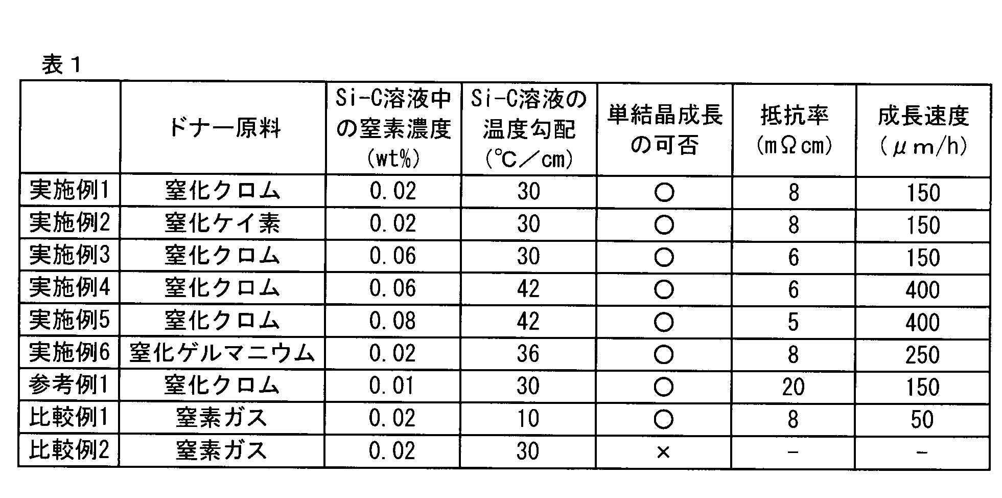
- Table 1 summarizes the conditions and results of Examples 1 to 6, Reference Example 1, and Comparative Examples 1 and 2.
Landscapes
- Chemical & Material Sciences (AREA)
- Engineering & Computer Science (AREA)
- Crystallography & Structural Chemistry (AREA)
- Materials Engineering (AREA)
- Metallurgy (AREA)
- Organic Chemistry (AREA)
- Inorganic Chemistry (AREA)
- Crystals, And After-Treatments Of Crystals (AREA)
- Liquid Deposition Of Substances Of Which Semiconductor Devices Are Composed (AREA)
Abstract
Description
Si-C溶液を形成するための原料またはSi-C溶液に、窒化物を添加することを含む、
n型SiC単結晶の製造方法である。
直径が12mm、厚みが700μmの円盤状4H-SiC単結晶であって、下面が(000-1)面を有する昇華法により作製したSiC単結晶を用意して、種結晶基板として用いた。種結晶基板は20mΩ・cmの抵抗率を有していた。種結晶基板の上面を、円柱形状の黒鉛軸の端面の略中央部に、黒鉛の接着剤を用いて接着した。
ドナー原料の窒化物としてSi3N4の粉末(高純度化学研究所製、3N)を、窒素を含むSi-C溶液の合計量に対して窒素原子量が0.02wt%含まれるように融液原料に加えて、窒素を含むSi-C溶液を形成したこと以外は、実施例1と同様の方法で結晶成長させた。
ドナー原料の窒化物としてCr2Nの粉末(三津和化学薬品製、3N)を、窒素を含むSi-C溶液の合計量に対して窒素原子量が0.06wt%含まれるように融液原料に加えて、窒素を含むSi-C溶液を形成したこと以外は、実施例1と同様の方法で結晶成長させた。
ドナー原料の窒化物としてCr2Nの粉末(高純度化学研究所製、3N)を、窒素を含むSi-C溶液の合計量に対して窒素原子量が0.06wt%含まれるように融液原料に加えて、窒素を含むSi-C溶液を形成したこと、並びにSi-C溶液の表面から10mmの範囲で溶液内部から溶液表面に向けて温度低下する温度勾配が42℃/cmとなるように上段コイル及び下段コイルの出力を制御したこと以外は、実施例1と同様の方法で結晶成長させた。
ドナー原料の窒化物としてCr2Nの粉末(高純度化学研究所製、3N)を、窒素を含むSi-C溶液の合計量に対して窒素原子量が0.08wt%含まれるように融液原料に加えて、窒素を含むSi-C溶液を形成したこと、並びにSi-C溶液の表面から10mmの範囲で溶液内部から溶液表面に向けて温度低下する温度勾配が42℃/cmとなるように上段コイル及び下段コイルの出力を制御したこと以外は、実施例1と同様の方法で結晶成長させた。
ドナー原料の窒化物としてGe3N4の粉末(高純度化学研究所製、3N)を、窒素を含むSi-C溶液の合計量に対して窒素原子量が0.02wt%含まれるように融液原料に加えて、窒素を含むSi-C溶液を形成したこと、並びにSi-C溶液の表面から10mmの範囲で溶液内部から溶液表面に向けて温度低下する温度勾配が36℃/cmとなるように上段コイル及び下段コイルの出力を制御したこと以外は、実施例1と同様の方法で結晶成長させた。
ドナー原料の窒化物としてCr2Nの粉末(三津和化学薬品製、3N)を、窒素を含むSi-C溶液の合計量に対して窒素原子量が0.01wt%含まれるように融液原料に加えて、窒素を含むSi-C溶液を形成したこと以外は、実施例1と同様の方法で結晶成長させた。
単結晶製造装置の内部を1×10⁻³Paに真空引きした後、アルゴンガス及び窒素ガスを導入して1気圧とし、単結晶製造装置の内部の空気を95vol%のアルゴン及び5vol%の窒素の混合ガスで置換した。このようにして、ドナー原料として窒化物に代えて窒素ガスを用い、窒化物を添加せずにSi-C溶液を形成したこと、並びにSi-C溶液の表面から10mmの範囲で溶液内部から溶液表面に向けて温度低下する温度勾配が10℃/cmとなるように上段コイル及び下段コイルの出力を制御したこと以外は、実施例1と同様の方法で結晶成長させた。このときのSi-C溶液中の平均窒素濃度は、窒素を含むSi-C溶液の全体量を基準にして、0.02wt%である。
Si-C溶液の表面から10mmの範囲で溶液内部から溶液表面に向けて温度低下する温度勾配が30℃/cmとなるように上段コイル及び下段コイルの出力を制御したこと以外は、比較例1と同様の方法で結晶成長させた。
10 黒鉛坩堝
12 黒鉛軸
14 種結晶基板
18 断熱材
22 高周波コイル
22A 上段高周波コイル
22B 下段高周波コイル
24 Si-C溶液
26 石英管
Claims (9)
- 内部から表面に向けて温度低下する温度勾配を有するSi-C溶液にSiC種結晶基板を接触させてn型SiC単結晶を結晶成長させる、n型SiC単結晶の製造方法であって、
前記Si-C溶液を形成するための原料または前記Si-C溶液に、窒化物を添加することを含む、
n型SiC単結晶の製造方法。 - 前記窒化物が、窒素及び遷移元素の化合物である、請求項1に記載の製造方法。
- 前記窒化物が、窒素及び典型元素の化合物である、請求項1に記載の製造方法。
- 前記窒化物が、窒素及び非金属元素の化合物である、請求項1に記載の製造方法。
- 前記窒化物が、窒素及び14族に属する元素の化合物である、請求項1に記載の製造方法。
- 前記窒化物が、窒素及び第4周期に属する元素の化合物である、請求項1に記載の製造方法。
- 前記窒化物が、窒化クロム、窒化ケイ素、窒化ゲルマニウム、窒化チタン、及び窒化ニッケルからなる群から選択される少なくとも1つである、請求項1に記載の製造方法。
- 前記窒化物の添加量が、窒素を含むSi-C溶液の全体量を基準にした窒素原子換算量で、0.02wt%以上である、請求項1~7のいずれか一項に記載の製造方法。
- 前記Si-C溶液の表面温度が1800~2200℃である、請求項1~8のいずれか一項に記載の製造方法。
Priority Applications (4)
| Application Number | Priority Date | Filing Date | Title |
|---|---|---|---|
| JP2014554171A JP5983772B2 (ja) | 2012-12-28 | 2013-04-01 | n型SiC単結晶の製造方法 |
| EP13866596.3A EP2940196B1 (en) | 2012-12-28 | 2013-04-01 | Method for producing n-type sic single crystal |
| US14/650,664 US9702057B2 (en) | 2012-12-28 | 2013-04-01 | Method for producing an n-type SiC single crystal from a Si—C solution comprising a nitride |
| CN201380067728.XA CN104870698B (zh) | 2012-12-28 | 2013-04-01 | n型SiC单晶的制造方法 |
Applications Claiming Priority (2)
| Application Number | Priority Date | Filing Date | Title |
|---|---|---|---|
| JP2012288239 | 2012-12-28 | ||
| JP2012-288239 | 2012-12-28 |
Publications (1)
| Publication Number | Publication Date |
|---|---|
| WO2014103394A1 true WO2014103394A1 (ja) | 2014-07-03 |
Family
ID=51020503
Family Applications (1)
| Application Number | Title | Priority Date | Filing Date |
|---|---|---|---|
| PCT/JP2013/059984 WO2014103394A1 (ja) | 2012-12-28 | 2013-04-01 | n型SiC単結晶の製造方法 |
Country Status (5)
| Country | Link |
|---|---|
| US (1) | US9702057B2 (ja) |
| EP (1) | EP2940196B1 (ja) |
| JP (1) | JP5983772B2 (ja) |
| CN (1) | CN104870698B (ja) |
| WO (1) | WO2014103394A1 (ja) |
Cited By (6)
| Publication number | Priority date | Publication date | Assignee | Title |
|---|---|---|---|---|
| CN105568362A (zh) * | 2014-10-31 | 2016-05-11 | 丰田自动车株式会社 | SiC单晶的制造方法 |
| WO2016117209A1 (ja) * | 2015-01-21 | 2016-07-28 | 住友電気工業株式会社 | 炭化珪素基板および炭化珪素基板の製造方法 |
| JP2016169126A (ja) * | 2015-03-13 | 2016-09-23 | 京セラ株式会社 | 結晶の製造方法 |
| JP2018095542A (ja) * | 2016-12-16 | 2018-06-21 | トヨタ自動車株式会社 | n型SiC単結晶の製造方法 |
| US10167570B2 (en) | 2013-08-30 | 2019-01-01 | Toyota Jidosha Kabushiki Kaisha | N-type SiC single crystal and method for its production |
| WO2024014246A1 (ja) * | 2022-07-14 | 2024-01-18 | 住友電気工業株式会社 | 炭化珪素結晶基板、炭化珪素エピタキシャル基板および炭化珪素半導体装置の製造方法 |
Families Citing this family (4)
| Publication number | Priority date | Publication date | Assignee | Title |
|---|---|---|---|---|
| US20170327968A1 (en) * | 2016-05-10 | 2017-11-16 | Toyota Jidosha Kabushiki Kaisha | SiC SINGLE CRYSTAL AND METHOD FOR PRODUCING SAME |
| US10577720B2 (en) | 2017-01-04 | 2020-03-03 | Cree, Inc. | Stabilized, high-doped silicon carbide |
| KR102302753B1 (ko) * | 2018-05-25 | 2021-09-14 | 주식회사 엘지화학 | 실리콘계 용융 조성물 및 이를 이용하는 실리콘카바이드 단결정의 제조 방법 |
| CN116926670B (zh) * | 2023-07-12 | 2024-04-16 | 通威微电子有限公司 | 一种用液相法制备碳化硅的方法和制得的碳化硅 |
Citations (4)
| Publication number | Priority date | Publication date | Assignee | Title |
|---|---|---|---|---|
| JP2007153719A (ja) * | 2005-12-08 | 2007-06-21 | Toyota Motor Corp | 炭化珪素単結晶の製造方法 |
| JP2008105896A (ja) | 2006-10-25 | 2008-05-08 | Toyota Motor Corp | SiC単結晶の製造方法 |
| JP2010189235A (ja) | 2009-02-19 | 2010-09-02 | Toyota Motor Corp | n型SiC単結晶の製造方法、それによって得られるn型SiC単結晶およびその用途 |
| JP2012250864A (ja) * | 2011-06-01 | 2012-12-20 | Sumitomo Electric Ind Ltd | 炭化珪素結晶インゴット、炭化珪素結晶ウエハおよび炭化珪素結晶インゴットの製造方法 |
Family Cites Families (6)
| Publication number | Priority date | Publication date | Assignee | Title |
|---|---|---|---|---|
| JPH0977594A (ja) | 1995-09-11 | 1997-03-25 | Nippon Steel Corp | 低抵抗単結晶炭化珪素の製造方法 |
| JP2000264790A (ja) * | 1999-03-17 | 2000-09-26 | Hitachi Ltd | 炭化珪素単結晶の製造方法 |
| JP4100228B2 (ja) * | 2002-04-15 | 2008-06-11 | 住友金属工業株式会社 | 炭化珪素単結晶とその製造方法 |
| JP4277926B1 (ja) * | 2007-11-27 | 2009-06-10 | トヨタ自動車株式会社 | 炭化珪素単結晶の成長法 |
| JP5304793B2 (ja) * | 2008-08-29 | 2013-10-02 | 新日鐵住金株式会社 | 炭化珪素単結晶の製造方法 |
| JP5487888B2 (ja) * | 2009-11-10 | 2014-05-14 | トヨタ自動車株式会社 | n型SiC単結晶の製造方法 |
-
2013
- 2013-04-01 JP JP2014554171A patent/JP5983772B2/ja active Active
- 2013-04-01 CN CN201380067728.XA patent/CN104870698B/zh active Active
- 2013-04-01 US US14/650,664 patent/US9702057B2/en active Active
- 2013-04-01 WO PCT/JP2013/059984 patent/WO2014103394A1/ja active Application Filing
- 2013-04-01 EP EP13866596.3A patent/EP2940196B1/en active Active
Patent Citations (4)
| Publication number | Priority date | Publication date | Assignee | Title |
|---|---|---|---|---|
| JP2007153719A (ja) * | 2005-12-08 | 2007-06-21 | Toyota Motor Corp | 炭化珪素単結晶の製造方法 |
| JP2008105896A (ja) | 2006-10-25 | 2008-05-08 | Toyota Motor Corp | SiC単結晶の製造方法 |
| JP2010189235A (ja) | 2009-02-19 | 2010-09-02 | Toyota Motor Corp | n型SiC単結晶の製造方法、それによって得られるn型SiC単結晶およびその用途 |
| JP2012250864A (ja) * | 2011-06-01 | 2012-12-20 | Sumitomo Electric Ind Ltd | 炭化珪素結晶インゴット、炭化珪素結晶ウエハおよび炭化珪素結晶インゴットの製造方法 |
Non-Patent Citations (1)
| Title |
|---|
| See also references of EP2940196A4 * |
Cited By (8)
| Publication number | Priority date | Publication date | Assignee | Title |
|---|---|---|---|---|
| US10167570B2 (en) | 2013-08-30 | 2019-01-01 | Toyota Jidosha Kabushiki Kaisha | N-type SiC single crystal and method for its production |
| CN105568362A (zh) * | 2014-10-31 | 2016-05-11 | 丰田自动车株式会社 | SiC单晶的制造方法 |
| JP2016088794A (ja) * | 2014-10-31 | 2016-05-23 | トヨタ自動車株式会社 | SiC単結晶の製造方法 |
| WO2016117209A1 (ja) * | 2015-01-21 | 2016-07-28 | 住友電気工業株式会社 | 炭化珪素基板および炭化珪素基板の製造方法 |
| CN107109695A (zh) * | 2015-01-21 | 2017-08-29 | 住友电气工业株式会社 | 碳化硅基板和碳化硅基板的制造方法 |
| JP2016169126A (ja) * | 2015-03-13 | 2016-09-23 | 京セラ株式会社 | 結晶の製造方法 |
| JP2018095542A (ja) * | 2016-12-16 | 2018-06-21 | トヨタ自動車株式会社 | n型SiC単結晶の製造方法 |
| WO2024014246A1 (ja) * | 2022-07-14 | 2024-01-18 | 住友電気工業株式会社 | 炭化珪素結晶基板、炭化珪素エピタキシャル基板および炭化珪素半導体装置の製造方法 |
Also Published As
| Publication number | Publication date |
|---|---|
| US9702057B2 (en) | 2017-07-11 |
| CN104870698A (zh) | 2015-08-26 |
| EP2940196A4 (en) | 2016-01-20 |
| JPWO2014103394A1 (ja) | 2017-01-12 |
| JP5983772B2 (ja) | 2016-09-06 |
| EP2940196B1 (en) | 2017-03-15 |
| US20150299896A1 (en) | 2015-10-22 |
| EP2940196A1 (en) | 2015-11-04 |
| CN104870698B (zh) | 2017-06-09 |
Similar Documents
| Publication | Publication Date | Title |
|---|---|---|
| JP5983772B2 (ja) | n型SiC単結晶の製造方法 | |
| CN102203330B (zh) | 碳化硅单晶的制造方法 | |
| JP5803519B2 (ja) | SiC単結晶の製造方法及び製造装置 | |
| JP5668724B2 (ja) | SiC単結晶のインゴット、SiC単結晶、及び製造方法 | |
| JP5741652B2 (ja) | n型SiC単結晶及びその製造方法 | |
| JP5434801B2 (ja) | SiC単結晶の製造方法 | |
| JP6090287B2 (ja) | SiC単結晶の製造方法 | |
| WO2017022535A1 (ja) | SiC単結晶の製造方法 | |
| TW201923169A (zh) | 碳化矽單晶之製造方法 | |
| JP5890377B2 (ja) | SiC単結晶の製造方法 | |
| JP6344374B2 (ja) | SiC単結晶及びその製造方法 | |
| JP2017202969A (ja) | SiC単結晶及びその製造方法 | |
| JP6380267B2 (ja) | SiC単結晶及びその製造方法 | |
| JP6030525B2 (ja) | SiC単結晶の製造方法 | |
| JP2018150193A (ja) | SiC単結晶の製造方法 | |
| JP2017202957A (ja) | SiC単結晶及びその製造方法 | |
| JP2016204188A (ja) | p型SiC単結晶 | |
| JP2019052074A (ja) | SiC単結晶の製造方法 |
Legal Events
| Date | Code | Title | Description |
|---|---|---|---|
| 121 | Ep: the epo has been informed by wipo that ep was designated in this application |
Ref document number: 13866596 Country of ref document: EP Kind code of ref document: A1 |
|
| ENP | Entry into the national phase |
Ref document number: 2014554171 Country of ref document: JP Kind code of ref document: A |
|
| WWE | Wipo information: entry into national phase |
Ref document number: 14650664 Country of ref document: US |
|
| REEP | Request for entry into the european phase |
Ref document number: 2013866596 Country of ref document: EP |
|
| WWE | Wipo information: entry into national phase |
Ref document number: 2013866596 Country of ref document: EP |
|
| NENP | Non-entry into the national phase |
Ref country code: DE |