WO2014077039A1 - 炭化珪素半導体装置の製造方法 - Google Patents
炭化珪素半導体装置の製造方法 Download PDFInfo
- Publication number
- WO2014077039A1 WO2014077039A1 PCT/JP2013/076435 JP2013076435W WO2014077039A1 WO 2014077039 A1 WO2014077039 A1 WO 2014077039A1 JP 2013076435 W JP2013076435 W JP 2013076435W WO 2014077039 A1 WO2014077039 A1 WO 2014077039A1
- Authority
- WO
- WIPO (PCT)
- Prior art keywords
- gas
- silicon carbide
- sic
- temperature
- semiconductor device
- Prior art date
- Legal status (The legal status is an assumption and is not a legal conclusion. Google has not performed a legal analysis and makes no representation as to the accuracy of the status listed.)
- Ceased
Links
Images


Classifications
-
- C—CHEMISTRY; METALLURGY
- C30—CRYSTAL GROWTH
- C30B—SINGLE-CRYSTAL GROWTH; UNIDIRECTIONAL SOLIDIFICATION OF EUTECTIC MATERIAL OR UNIDIRECTIONAL DEMIXING OF EUTECTOID MATERIAL; REFINING BY ZONE-MELTING OF MATERIAL; PRODUCTION OF A HOMOGENEOUS POLYCRYSTALLINE MATERIAL WITH DEFINED STRUCTURE; SINGLE CRYSTALS OR HOMOGENEOUS POLYCRYSTALLINE MATERIAL WITH DEFINED STRUCTURE; AFTER-TREATMENT OF SINGLE CRYSTALS OR A HOMOGENEOUS POLYCRYSTALLINE MATERIAL WITH DEFINED STRUCTURE; APPARATUS THEREFOR
- C30B25/00—Single-crystal growth by chemical reaction of reactive gases, e.g. chemical vapour-deposition growth
- C30B25/02—Epitaxial-layer growth
-
- C—CHEMISTRY; METALLURGY
- C30—CRYSTAL GROWTH
- C30B—SINGLE-CRYSTAL GROWTH; UNIDIRECTIONAL SOLIDIFICATION OF EUTECTIC MATERIAL OR UNIDIRECTIONAL DEMIXING OF EUTECTOID MATERIAL; REFINING BY ZONE-MELTING OF MATERIAL; PRODUCTION OF A HOMOGENEOUS POLYCRYSTALLINE MATERIAL WITH DEFINED STRUCTURE; SINGLE CRYSTALS OR HOMOGENEOUS POLYCRYSTALLINE MATERIAL WITH DEFINED STRUCTURE; AFTER-TREATMENT OF SINGLE CRYSTALS OR A HOMOGENEOUS POLYCRYSTALLINE MATERIAL WITH DEFINED STRUCTURE; APPARATUS THEREFOR
- C30B25/00—Single-crystal growth by chemical reaction of reactive gases, e.g. chemical vapour-deposition growth
- C30B25/02—Epitaxial-layer growth
- C30B25/10—Heating of the reaction chamber or the substrate
-
- C—CHEMISTRY; METALLURGY
- C30—CRYSTAL GROWTH
- C30B—SINGLE-CRYSTAL GROWTH; UNIDIRECTIONAL SOLIDIFICATION OF EUTECTIC MATERIAL OR UNIDIRECTIONAL DEMIXING OF EUTECTOID MATERIAL; REFINING BY ZONE-MELTING OF MATERIAL; PRODUCTION OF A HOMOGENEOUS POLYCRYSTALLINE MATERIAL WITH DEFINED STRUCTURE; SINGLE CRYSTALS OR HOMOGENEOUS POLYCRYSTALLINE MATERIAL WITH DEFINED STRUCTURE; AFTER-TREATMENT OF SINGLE CRYSTALS OR A HOMOGENEOUS POLYCRYSTALLINE MATERIAL WITH DEFINED STRUCTURE; APPARATUS THEREFOR
- C30B25/00—Single-crystal growth by chemical reaction of reactive gases, e.g. chemical vapour-deposition growth
- C30B25/02—Epitaxial-layer growth
- C30B25/16—Controlling or regulating
-
- C—CHEMISTRY; METALLURGY
- C30—CRYSTAL GROWTH
- C30B—SINGLE-CRYSTAL GROWTH; UNIDIRECTIONAL SOLIDIFICATION OF EUTECTIC MATERIAL OR UNIDIRECTIONAL DEMIXING OF EUTECTOID MATERIAL; REFINING BY ZONE-MELTING OF MATERIAL; PRODUCTION OF A HOMOGENEOUS POLYCRYSTALLINE MATERIAL WITH DEFINED STRUCTURE; SINGLE CRYSTALS OR HOMOGENEOUS POLYCRYSTALLINE MATERIAL WITH DEFINED STRUCTURE; AFTER-TREATMENT OF SINGLE CRYSTALS OR A HOMOGENEOUS POLYCRYSTALLINE MATERIAL WITH DEFINED STRUCTURE; APPARATUS THEREFOR
- C30B25/00—Single-crystal growth by chemical reaction of reactive gases, e.g. chemical vapour-deposition growth
- C30B25/02—Epitaxial-layer growth
- C30B25/18—Epitaxial-layer growth characterised by the substrate
- C30B25/20—Epitaxial-layer growth characterised by the substrate the substrate being of the same materials as the epitaxial layer
-
- C—CHEMISTRY; METALLURGY
- C30—CRYSTAL GROWTH
- C30B—SINGLE-CRYSTAL GROWTH; UNIDIRECTIONAL SOLIDIFICATION OF EUTECTIC MATERIAL OR UNIDIRECTIONAL DEMIXING OF EUTECTOID MATERIAL; REFINING BY ZONE-MELTING OF MATERIAL; PRODUCTION OF A HOMOGENEOUS POLYCRYSTALLINE MATERIAL WITH DEFINED STRUCTURE; SINGLE CRYSTALS OR HOMOGENEOUS POLYCRYSTALLINE MATERIAL WITH DEFINED STRUCTURE; AFTER-TREATMENT OF SINGLE CRYSTALS OR A HOMOGENEOUS POLYCRYSTALLINE MATERIAL WITH DEFINED STRUCTURE; APPARATUS THEREFOR
- C30B29/00—Single crystals or homogeneous polycrystalline material with defined structure characterised by the material or by their shape
- C30B29/10—Inorganic compounds or compositions
- C30B29/36—Carbides
-
- H—ELECTRICITY
- H10—SEMICONDUCTOR DEVICES; ELECTRIC SOLID-STATE DEVICES NOT OTHERWISE PROVIDED FOR
- H10D—INORGANIC ELECTRIC SEMICONDUCTOR DEVICES
- H10D30/00—Field-effect transistors [FET]
- H10D30/60—Insulated-gate field-effect transistors [IGFET]
-
- H—ELECTRICITY
- H10—SEMICONDUCTOR DEVICES; ELECTRIC SOLID-STATE DEVICES NOT OTHERWISE PROVIDED FOR
- H10D—INORGANIC ELECTRIC SEMICONDUCTOR DEVICES
- H10D62/00—Semiconductor bodies, or regions thereof, of devices having potential barriers
- H10D62/40—Crystalline structures
- H10D62/405—Orientations of crystalline planes
-
- H—ELECTRICITY
- H10—SEMICONDUCTOR DEVICES; ELECTRIC SOLID-STATE DEVICES NOT OTHERWISE PROVIDED FOR
- H10D—INORGANIC ELECTRIC SEMICONDUCTOR DEVICES
- H10D62/00—Semiconductor bodies, or regions thereof, of devices having potential barriers
- H10D62/80—Semiconductor bodies, or regions thereof, of devices having potential barriers characterised by the materials
- H10D62/83—Semiconductor bodies, or regions thereof, of devices having potential barriers characterised by the materials being Group IV materials, e.g. B-doped Si or undoped Ge
- H10D62/832—Semiconductor bodies, or regions thereof, of devices having potential barriers characterised by the materials being Group IV materials, e.g. B-doped Si or undoped Ge being Group IV materials comprising two or more elements, e.g. SiGe
- H10D62/8325—Silicon carbide
-
- H—ELECTRICITY
- H10—SEMICONDUCTOR DEVICES; ELECTRIC SOLID-STATE DEVICES NOT OTHERWISE PROVIDED FOR
- H10P—GENERIC PROCESSES OR APPARATUS FOR THE MANUFACTURE OR TREATMENT OF DEVICES COVERED BY CLASS H10
- H10P14/00—Formation of materials, e.g. in the shape of layers or pillars
- H10P14/20—Formation of materials, e.g. in the shape of layers or pillars of semiconductor materials
- H10P14/24—Formation of materials, e.g. in the shape of layers or pillars of semiconductor materials using chemical vapour deposition [CVD]
-
- H—ELECTRICITY
- H10—SEMICONDUCTOR DEVICES; ELECTRIC SOLID-STATE DEVICES NOT OTHERWISE PROVIDED FOR
- H10P—GENERIC PROCESSES OR APPARATUS FOR THE MANUFACTURE OR TREATMENT OF DEVICES COVERED BY CLASS H10
- H10P14/00—Formation of materials, e.g. in the shape of layers or pillars
- H10P14/20—Formation of materials, e.g. in the shape of layers or pillars of semiconductor materials
- H10P14/29—Formation of materials, e.g. in the shape of layers or pillars of semiconductor materials characterised by the substrates
- H10P14/2901—Materials
- H10P14/2902—Materials being Group IVA materials
- H10P14/2904—Silicon carbide
-
- H—ELECTRICITY
- H10—SEMICONDUCTOR DEVICES; ELECTRIC SOLID-STATE DEVICES NOT OTHERWISE PROVIDED FOR
- H10P—GENERIC PROCESSES OR APPARATUS FOR THE MANUFACTURE OR TREATMENT OF DEVICES COVERED BY CLASS H10
- H10P14/00—Formation of materials, e.g. in the shape of layers or pillars
- H10P14/20—Formation of materials, e.g. in the shape of layers or pillars of semiconductor materials
- H10P14/32—Formation of materials, e.g. in the shape of layers or pillars of semiconductor materials characterised by intermediate layers between substrates and deposited layers
- H10P14/3202—Materials thereof
- H10P14/3204—Materials thereof being Group IVA semiconducting materials
- H10P14/3208—Silicon carbide
-
- H—ELECTRICITY
- H10—SEMICONDUCTOR DEVICES; ELECTRIC SOLID-STATE DEVICES NOT OTHERWISE PROVIDED FOR
- H10P—GENERIC PROCESSES OR APPARATUS FOR THE MANUFACTURE OR TREATMENT OF DEVICES COVERED BY CLASS H10
- H10P14/00—Formation of materials, e.g. in the shape of layers or pillars
- H10P14/20—Formation of materials, e.g. in the shape of layers or pillars of semiconductor materials
- H10P14/34—Deposited materials, e.g. layers
- H10P14/3402—Deposited materials, e.g. layers characterised by the chemical composition
- H10P14/3404—Deposited materials, e.g. layers characterised by the chemical composition being Group IVA materials
- H10P14/3408—Silicon carbide
Definitions
- the present invention relates to a method of manufacturing a silicon carbide semiconductor device.
- a 4H-SiC single crystal film (hereinafter referred to as a SiC epitaxial film) is formed on a 4H-SiC semiconductor substrate (hereinafter referred to as 4H-SiC substrate) Is epitaxially grown to fabricate a SiC single crystal substrate.
- a chemical vapor deposition (CVD) method is known as an epitaxial growth method.
- a SiC single crystal substrate on which a SiC epitaxial film is deposited by chemical vapor deposition is thermally decomposed in a carrier gas from a raw material gas flowing into a reactor (chamber) to form a 4H-SiC substrate crystal. It is fabricated by continuously depositing silicon (Si) atoms following a lattice.
- Si silicon
- monosilane (SiH 4 ) gas and dimethylmethane (C 3 H 8 ) gas are used as source gases, and hydrogen (H 2 ) gas is used as a carrier gas.
- nitrogen (N 2 ) gas or trimethylaluminum (TMA) gas is appropriately added as a doping gas.
- the growth rate is generally about several ⁇ m / h, an epitaxial film can not be grown at high speed. Therefore, it takes a long time to grow an epitaxial film with a thickness of 100 ⁇ m or more, which is necessary to produce a high breakdown voltage device, and therefore, an increase in the epitaxial growth rate is required industrially. Further, in the high breakdown voltage device, since the epitaxial film having a thickness of 100 ⁇ m or more is provided as the drift layer, the conduction loss is increased as the breakdown voltage is increased.
- Non-Patent Document 1 Japanese Patent Document 1
- a method of reducing carbon vacancies in a SiC epitaxial film a method of forming a SiC epitaxial film by chemical vapor deposition and then performing ion implantation and heat treatment of carbon and sacrificial oxidation for a long time is proposed. (See, for example, the following non-patent documents 2 and 3).
- El Strasta (L. Storasta), 4 others, Deep Levels Created by Low Energy Energy Electron Radiation In 4H-SiC (Deep levels created by low energy electron irradiation in 4H-SiC), Journal of Applied Physics (AIP: Journal of Applied Physics) Applied Physics) (US), American Institute of Physics, November 1, 2004, Vol. 96, No. 9, p. 4909-4915 El Strasta (L.Storasta), 1 person, Reduction of Traps and Improvement of Carrier Lifetime in 4H-SiC Epilayers by Ion Implantation (Reduction of traps and improvement of carrier lifetime in 4H-SiC epilayers by ion implantation, Applied Physics Letters (AIP), (USA), American Institute of Physics, 2007, vol.
- Non-Patent Documents 2 and 3 described above after the SiC single crystal substrate in which the SiC epitaxial film is stacked on the 4H-SiC substrate is manufactured, the SiC epitaxial is formed in addition to the step of forming the element structure on the SiC single crystal substrate. It is necessary to carry out an additional step to reduce carbon vacancies in the film, and there is a problem that the throughput is reduced.
- the present invention provides a method for manufacturing a silicon carbide semiconductor device having a long carrier lifetime without performing an additional step after producing a silicon carbide single crystal substrate by a chemical vapor deposition method. Intended to provide.
- the method for manufacturing a silicon carbide semiconductor device has the following features. First, a growth step of growing a silicon carbide single crystal film at a first temperature on a silicon carbide semiconductor substrate by chemical vapor deposition is performed. Next, after the growth step, a first cooling step of cooling the silicon carbide semiconductor substrate to a second temperature lower than the first temperature from the first temperature is performed in a gas atmosphere containing carbon. Next, after the first cooling step, a second cooling step of cooling the silicon carbide semiconductor substrate to a third temperature lower than the second temperature is performed under a hydrogen gas atmosphere.
- the first cooling step is performed in a gas atmosphere containing carbon and chlorine.
- the first cooling step is performed in a mixed gas atmosphere in which a gas containing carbon and chlorine is added to a hydrogen gas.
- the mixed gas atmosphere is a gas containing the carbon in a ratio of 0.1% to 0.3% with respect to the hydrogen gas It is characterized by being added.
- the mixed gas atmosphere contains a gas containing chlorine at a ratio of 0.5% to 1.0% with respect to the hydrogen gas. It is characterized by being added.
- the density of Z 1/2 centers present in the silicon carbide single crystal film is 6.7 ⁇ 10. 12 and cm -3, characterized by the EH 6/7 center density 2.7 ⁇ 10 12 cm -3 of that present in the silicon carbide single crystal film.
- a silicon carbide single crystal film is grown on a silicon carbide semiconductor substrate, cooling is performed in a mixed gas atmosphere in which a gas containing carbon is added to a hydrogen gas, whereby the carbon gas is contained.
- the carbon vacancies in the silicon carbide single crystal film can be filled with carbon atoms, and carbon vacancies in the silicon carbide single crystal film can be reduced. Therefore, it is possible to reduce the Z 1/2 center and the EH 6/7 center, which are lifetime killers generated due to carbon vacancies in the silicon carbide single crystal film. Thereby, the carrier lifetime of the silicon carbide single crystal film can be extended.
- carbon vacancies in the silicon carbide single crystal film are formed during the process for producing the silicon carbide single crystal substrate by the chemical vapor deposition method, that is, during the formation process of the silicon carbide single crystal film performed in the reaction furnace. Can be reduced.
- a silicon carbide semiconductor device having a long carrier lifetime without performing an additional step after producing a silicon carbide single crystal substrate by a chemical vapor deposition method.
- FIG. 3 is a flowchart showing an outline of a method of manufacturing the silicon carbide semiconductor device according to the first embodiment.
- FIG. 7 is a cross-sectional view showing a state in the middle of manufacturing the silicon carbide semiconductor device according to the first embodiment. It is a graph which shows the relationship between the gas addition amount at the time of cooling of the manufacturing method of the silicon carbide semiconductor device of a comparative example, and the crystal defect density in an epitaxial film. 6 is a table showing the relationship between the amount of added gas at cooling and the crystal defect density in an epitaxial film in the method for manufacturing a silicon carbide semiconductor device according to the first embodiment.
- FIG. 7 is a cross-sectional view showing a state in the middle of manufacturing the silicon carbide semiconductor device according to the first embodiment. It is a graph which shows the relationship between the gas addition amount at the time of cooling of the manufacturing method of the silicon carbide semiconductor device of a comparative example, and the crystal defect density in an epitaxial film. 6 is a table showing the relationship between the amount of added
- FIG. 16 is a table showing the relationship between the amount of added gas at the time of cooling and the crystal defect density in the epitaxial film in the method for manufacturing a silicon carbide semiconductor device according to the second embodiment.
- FIG. 16 is a characteristic diagram showing a relationship between a gas addition amount at cooling and a film thickness of an epitaxial film in a method of manufacturing a silicon carbide semiconductor device according to a second embodiment.
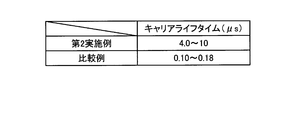
- FIG. 16 is a chart showing the carrier lifetime of the silicon carbide semiconductor device manufactured by the method for manufacturing a silicon carbide semiconductor device according to the second embodiment.
- Embodiment 1 A method of manufacturing a silicon carbide semiconductor device according to the first embodiment will be described by taking a case of manufacturing (manufacturing) a semiconductor device using four-layer periodic hexagonal crystal (4H—SiC) of silicon carbide as a semiconductor material.
- FIG. 1A is a flowchart showing an outline of a method of manufacturing a silicon carbide semiconductor device according to a first embodiment.
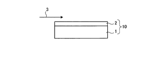
- FIG. 1B is a cross-sectional view showing a state in the middle of manufacture of the silicon carbide semiconductor device according to the first embodiment.
- a substrate (4H-SiC substrate) 1 made of 4H-SiC is prepared, and cleaned by a general organic cleaning method or RCA cleaning method (step S1).
- the main surface of the 4H—SiC substrate 1 may be, for example, a (0001) Si 4 ° off surface.
- a reactor for growing a 4H-SiC single crystal film (hereinafter referred to as a SiC epitaxial film (silicon carbide single crystal film)) 2 by chemical vapor deposition (CVD) method
- 4H-SiC substrate 1 is inserted (step S2).
- the inside of the reaction furnace is evacuated to a vacuum of, for example, 1 ⁇ 10 ⁇ 3 Pa or less.
- hydrogen (H 2 ) gas purified by a general purifier is introduced into the reactor, for example, at a flow rate of 20 L / min for 15 minutes, and the atmosphere in the reactor is replaced with an H 2 atmosphere (step S3) .
- step S 4 the surface of the 4H—SiC substrate 1 is cleaned by chemical etching with H 2 gas. Specifically, with the H 2 gas introduced at 20 L / min, the reactor is heated, for example, by high frequency induction. Then, the inside of the reactor is raised to 1600 ° C. and held at this temperature for 10 minutes. Thus, the surface of the 4H-SiC substrate 1 is cleaned.
- the temperature in the reactor is measured, for example, by a radiation thermometer and controlled by control means (not shown).
- step S5 the temperature in the reactor is adjusted to a first temperature for growing the SiC epitaxial film 2, specifically, for example, 1700 ° C.
- step S6 the temperature in the reactor is adjusted to a first temperature for growing the SiC epitaxial film 2, specifically, for example, 1700 ° C.
- step S6 the source gas, a gas to be added to the source gas (hereinafter referred to as an additive gas) and a doping gas Introduce (step S6).
- the source gas, the additive gas, the doping gas, and the carrier gas are collectively shown by arrow 3.
- a gas containing silicon (Si) and a gas containing carbon (C) are used as source gases.
- the gas containing silicon may be, for example, monosilane (hereinafter referred to as SiH 4 / H 2 ) gas diluted with hydrogen.
- the gas containing carbon (hereinafter referred to as the first carbon containing gas) may be, for example, dimethylmethane diluted with hydrogen (hereinafter referred to as C 3 H 8 / H 2 ) gas.
- the gas containing the first carbon is, for example, adjusted so that the ratio of the number of carbon atoms to the number of silicon atoms in the gas containing silicon (hereinafter referred to as C / Si ratio) is 1.0. May be
- a gas containing chlorine (Cl) may be used as the additive gas. That is, in step S7 described later, epitaxial growth is performed by a halide CVD method using a halogen compound.
- the gas containing chlorine may be, for example, hydrogen chloride (HCl) gas.
- the gas containing chlorine may be adjusted so that, for example, the ratio of the number of chlorine atoms to the number of silicon atoms in the gas containing silicon (hereinafter referred to as the Cl / Si ratio) is 3.0.
- nitrogen (N 2 ) gas may be used as the doping gas.
- a SiC epitaxial film 2 is grown on the surface of the 4H-SiC substrate 1 by chemical vapor deposition (CVD) using the source gas, additive gas, doping gas and carrier gas introduced in step S6 (step S7). ). Specifically, the temperature in the reaction furnace is maintained at a temperature of 1700 ° C. (first temperature), and the raw material gas is pyrolyzed with the carrier gas to form the SiC epitaxial film 2 on the 4H-SiC substrate 1 for 30 minutes. Grow up.
- CVD chemical vapor deposition
- Step S8 an atmosphere of a gas containing carbon diluted with hydrogen gas (hereinafter, referred to as a gas containing a second carbon) until the temperature in the reactor falls to a second temperature lower than the first temperature (temperature lowering)
- a gas containing a second carbon an atmosphere of a gas containing carbon diluted with hydrogen gas (hereinafter, referred to as a gas containing a second carbon) until the temperature in the reactor falls to a second temperature lower than the first temperature (temperature lowering)
- a gas containing a second carbon an atmosphere of a gas containing carbon diluted with hydrogen gas
- step S8 for example, C 3 H 8 gas is added as a second carbon-containing gas while hydrogen gas as a carrier gas is introduced at a flow rate of 20 L / min into the reaction furnace (ie, C 3 H 8 / H 2 gas atmosphere).
- the 4H—SiC substrate 1 on which the SiC epitaxial film 2 is laminated is exposed until the temperature in the reactor reaches, eg, 1300 ° C. (second temperature).
- the amount of the second carbon-containing gas added is, for example, 0.1% or more and 0.3% or less, preferably 0.2% or more and 0.3% or less, with respect to hydrogen gas (20 L / min). It is good. The reason will be described later.
- the second temperature is preferably 1300 ° C. or more and 1500 ° C. or less.
- the reason is that by lowering the temperature to, for example, 1300 ° C. from the growth temperature, the cooling time with the second carbon-containing gas can be extended, and the supply time of the carbon (C) -containing gas can be extended.
- the second temperature is 1300.degree. The reason is to lengthen the cooling time with the second carbon-containing gas as described above, and when the second temperature becomes 1300 ° C. or less, C is deposited and the inside of the growth furnace (reactor) This is to prevent the members from being discolored.
- step S9 with hydrogen gas as a carrier gas introduced at a flow rate of 20 L / min into the reaction furnace, the SiC epitaxial film is heated until the temperature in the reaction furnace reaches, for example, room temperature (25 ° C .: third temperature).
- the 4H-SiC substrate 1 on which 2 is stacked is cooled.
- the carbon vacancies in the SiC epitaxial film 2 are reduced, and the SiC single crystal substrate 10 provided with the SiC epitaxial film 2 with few crystal defects that become lifetime killers is manufactured.
- the SiC single crystal substrate 10 is taken out of the reaction furnace and a desired device structure (not shown) is formed (step S10), whereby the SiC semiconductor device is completed.
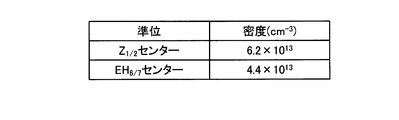
- FIG. 2 is a chart showing the relationship between the amount of added gas at the time of cooling and the crystal defect density in the epitaxial film in the method for manufacturing a silicon carbide semiconductor device of the comparative example.
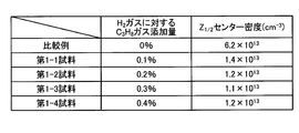
- FIG. 3 is a chart showing the relationship between the amount of added gas at the time of cooling and the crystal defect density in the epitaxial film in the method for manufacturing a silicon carbide semiconductor device according to the first embodiment.
- hydrogen gas was introduced into the reactor at a flow rate of 20 L / min as a carrier gas.
- the gas containing silicon SiH 4 / H 2 gas diluted with hydrogen by 50%, and C 3 H 8 / H 2 gas diluted with first carbon and hydrogen by 20% were used.
- the C / Si ratio was 1.0.
- HCl gas was used as the additive gas, and the Cl / Si ratio was 3.0.
- the flow rates of SiH 4 / H 2 gas, C 3 H 8 / H 2 gas and HCl gas were set to 200 sccm, 166 sccm and 300 sccm, respectively.
- Nitrogen gas was used as a doping gas, and the flow rate of nitrogen gas was adjusted so that the carrier concentration of the SiC epitaxial film 2 was 2 ⁇ 10 15 / cm ⁇ 3 .
- the first temperature for growing the SiC epitaxial film 2 is 1700 ° C., and the growth time of the SiC epitaxial film 2 is 30 minutes.
- step S8 hydrogen gas (20 L / min) is introduced, and C 3 H 8 gas is added as a second carbon-containing gas (ie, C 3 H 8 / H 2 gas atmosphere), and the temperature in the reactor is set to It was lowered from 1700 ° C to 1300 ° C.
- step S9 hydrogen gas was introduced into the reactor at a flow rate of 20 L / min. Further, in step S8, the addition amount of C 3 H 8 gas with respect to hydrogen gas was variously changed, and a plurality of first examples were manufactured (hereinafter, samples 1-1 to 1-4).
- step S8 the added amounts of C 3 H 8 gas to hydrogen gas (20 L / min) were 0.1% (equivalent to 20 sccm) and 0. 1 to 1-4, respectively. The values are 2% (equivalent to 40 sccm), 0.3% (equivalent to 60 sccm) and 0.4% (equivalent to 80 sccm). The numbers in parentheses are the amounts of C 3 H 8 gas added. Then, with respect to the 1-1 to 1-4 samples, Z 1 / clearly observed in the SiC epitaxial film 2 in a temperature range of 80 K to 680 K by isothermal capacitance transient spectroscopy (ICTS). 2 center density was measured. The results are shown in FIG. In FIG. 3, the addition amount of C 3 H 8 gas to hydrogen gas is 0% in a comparative example described later.
- ICTS isothermal capacitance transient spectroscopy
- step S8 a sample was prepared in which the 4H—SiC substrate on which the SiC epitaxial film was stacked was cooled without introducing a C 3 H 8 gas (hereinafter, referred to as a comparative example). That is, in the comparative example, the process from step S8 to the process of step S9 are performed in a state where only hydrogen gas is introduced at a flow rate of 20 L / min into the reaction furnace. The conditions other than that at the time of producing a comparative example are the same as that of a 1st example. In the comparative example, the Z 1/2 center density and the EH 6/7 center density clearly observed in the SiC epitaxial film 2 were measured by isothermal capacity transient spectroscopy in the temperature range of 80K to 680K. The results are shown in FIG.
- the Z 1/2 center density in the comparative example is 6.2 ⁇ 10 13 cm ⁇ 3
- the Z 1/2 center density in the first embodiment is 1.4 ⁇ It was 10 13 cm -3 or less. Therefore, it was confirmed that the first example can lower the Z 1/2 center density more than the comparative example.
- the reason is that the carbon atoms in the C 3 H 8 gas are taken into the SiC epitaxial film 2, and the taken-in carbon atoms fill the carbon vacancies in the SiC epitaxial film 2, and the carbon vacancies in the SiC epitaxial film 2 This is because the holes are reduced.
- EH 6/7 centers generated due to carbon vacancies as well as Z 1/2 centers are also reduced. Therefore, the first embodiment can lower the EH 6/7 center density more than the comparative example.
- the Z 1/2 center density decreases as the amount of C 3 H 8 gas added in step S8 increases.
- the Z 1/2 center density when the addition amount of C 3 H 8 gas to hydrogen gas is 0.4% is 0.2% to 0.3% of the addition amount of C 3 H 8 gas to hydrogen gas.
- the density was approximately the same as the Z 1/2 center density when being%. That is, when the amount of C 3 H 8 gas added to hydrogen gas is 0.4% or more, no further decrease in Z 1/2 center density is observed. Therefore, in step S8, the addition amount of C 3 H 8 gas to hydrogen gas should be 0.1% to 0.3%, preferably 0.2% to 0.3%. Good.
- the SiC epitaxial film is grown on the 4H—SiC substrate, cooling is performed in a mixed gas atmosphere in which the second carbon-containing gas is added to the hydrogen gas.
- carbon vacancies in the SiC epitaxial film can be filled with carbon atoms in the second carbon-containing gas, and carbon vacancies in the SiC epitaxial film can be reduced.
- the carrier lifetime of the SiC epitaxial film can be extended.
- carbon vacancies in the SiC epitaxial film can be reduced during the process for producing the SiC single crystal substrate by the chemical vapor deposition method, that is, during the process of forming the SiC epitaxial film performed in the reaction furnace. it can. Therefore, it is possible to provide a silicon carbide semiconductor device having a long carrier lifetime, without performing additional steps such as ion implantation and sacrificial oxidation as in the related art after producing a SiC single crystal substrate. Therefore, the throughput can be improved in manufacturing a silicon carbide semiconductor device having a long carrier lifetime.
- the method of manufacturing a silicon carbide semiconductor device according to the second embodiment differs from the method of manufacturing a silicon carbide semiconductor device according to the first embodiment in the following three points.
- the first difference is that the C / Si ratio of the source gas is 1.25.
- the second difference is that the first temperature for growing the SiC epitaxial film 2 is 1640 ° C.
- the third difference is that a gas containing chlorine (hereinafter referred to as a gas containing a second chlorine) is further added in step S8.
- step S5 the temperature in the reaction furnace is adjusted to 1640 ° C. (first temperature).
- step S6 a source gas is introduced such that the C / Si ratio is 1.25.
- step S7 the growth temperature of the SiC epitaxial film 2 is set to 1640.degree.
- step S8 the temperature in the reactor is lowered from 1640 ° C. to a second temperature (eg, 1300 ° C.).
- the atmosphere in the reactor at this time is an atmosphere of a gas containing second carbon diluted with hydrogen gas and a gas containing second chlorine.
- HCl gas may be used as the second chlorine-containing gas.
- the addition amount of the second chlorine-containing gas may be, for example, in the range of 0.5% to 1.0% with respect to hydrogen gas (20 L / min).
- the reason will be described later.
- the first temperature may be 1550 ° C. or more and 1700 ° C. or less. The reason is that 3C—SiC is formed at a low temperature, and step bunching occurs on the surface at a high temperature of 1700 ° C. or more, resulting in surface unevenness.
- the first temperature is 1640.degree. The reason is to ensure that 4H-SiC is grown without the occurrence of step bunching.
- the other conditions of the second embodiment are the same as those of the first embodiment.
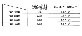
- FIG. 4 is a chart showing the relationship between the amount of gas added at the time of cooling and the crystal defect density in the epitaxial film in the method for manufacturing a silicon carbide semiconductor device according to the second embodiment.
- a SiC single crystal substrate 10 in which the SiC epitaxial film 2 is stacked on the 4H—SiC substrate 1 was manufactured (hereinafter, referred to as a second embodiment).
- the C / Si ratio is set to 1.25.
- the first temperature for growing the SiC epitaxial film 2 was set to 1640.degree.
- step S8 hydrogen gas (20 L / min) is introduced, C 3 H 8 gas is added as a second carbon-containing gas, and HCl gas is added as a second chlorine-containing gas (ie, C 3 H 8 / HCl / H 2 gas atmosphere), the temperature in the reactor was lowered from 1640 ° C. to 1300 ° C.
- the addition amount of C 3 H 8 gas to hydrogen gas is 0.2% (equivalent to 40 sccm), and the addition amount of HCl gas to hydrogen gas is variously changed to fabricate a plurality of second examples. (Hereinafter referred to as samples 2-1 to 2-4).
- the samples 2-1 to 2-4 each added 0% of the added amount of HCl gas to hydrogen gas (20 L / min) in step S8 (that is, only 0.2% of C 3 H 8 gas). There are approximately 0.5% (equivalent to 100 sccm), 1.0% (equivalent to 200 sccm) and 1.5% (equivalent to 300 sccm). The numbers in parentheses are the addition amount of HCl gas.
- the remaining structure of the second embodiment is similar to that of the first embodiment.
- the Z 1/2 center density clearly observed in the SiC epitaxial film 2 was measured in the temperature range of 80 K to 680 K by isothermal capacity transient spectroscopy. The results are shown in FIG.
- the second sample to which the HCl gas is added is selected.
- the Z 1/2 center density in the 2 to 2-4 samples was 7.9 ⁇ 10 12 cm ⁇ 3 or less. Therefore, it was confirmed that the samples 2-2 to 2-4 of the second embodiment can lower the Z 1/2 center density more than the first embodiment.
- the reason is as follows. By adding the C 3 H 8 gas, the same effect as that of the first embodiment can be obtained. Furthermore, the silicon atoms in the SiC epitaxial film 2 are evaporated by the HCl gas, and unbonded carbon atoms remain in the SiC epitaxial film 2.
- FIG. 5 is a characteristic diagram showing the relationship between the gas addition amount at cooling and the film thickness of the epitaxial film in the method for manufacturing a silicon carbide semiconductor device according to the second embodiment. From the results shown in FIG. 5, it was confirmed that the film thickness of the SiC epitaxial film 2 becomes thinner as the addition amount of HCl gas to the hydrogen gas increases. The reason for this is that the SiC epitaxial film 2 is etched by chlorine atoms in HCl gas.
- the film thickness of the SiC epitaxial film 2 was greatly reduced in the second to fourth samples (the addition amount of HCl gas to hydrogen gas: 1.5%). Therefore, in order to suppress the film thickness of SiC epitaxial film 2 to a desired amount of reduction and to reduce carbon vacancies in SiC epitaxial film 2, the addition amount of HCl gas to hydrogen gas is 0.5% to 1.%. It is preferable to make it 0%.
- the samples 2-2 to 2-4 of the second embodiment carbon vacancies in the SiC epitaxial film 2 can be reduced as compared with the first embodiment, and thus carbon vacancy is the same as in the Z 1/2 center.
- the EH 6/7 centers resulting from the holes are also reduced compared to the first embodiment. Therefore, the 2-2 to 2-4 samples of the second embodiment can lower the EH 6/7 center density more than the first embodiment. For example, it was confirmed that the EH 6/7 center density is 2.7 ⁇ 10 ⁇ 12 cm ⁇ 3 in the second to third samples (the addition amount of HCl gas to hydrogen gas: 1.0%).
- FIG. 6 is a chart showing the carrier lifetime of the silicon carbide semiconductor device manufactured by the method for manufacturing a silicon carbide semiconductor device according to the second embodiment.
- the carrier lifetime in the comparative example was 0.10 ⁇ s to 0.18 ⁇ s.
- the carrier lifetime in the second embodiment was 4.0 ⁇ s to 10 ⁇ s, and it was confirmed that the carrier lifetime can be made longer than that of the comparative example.
- the silicon atoms in the SiC epitaxial film are further added by adding the second chlorine-containing gas to the gas atmosphere during cooling of the 4H-SiC substrate on which the SiC epitaxial film is stacked.
- the carbon atoms in the SiC epitaxial film are filled with the carbon atoms that are dissolved and remain. Therefore, carbon vacancies in the SiC epitaxial film can be reduced as compared with the case where only the second carbon-containing gas is added.
- the present invention can be variously modified, and in each embodiment described above, for example, types of source gas, additive gas, carrier gas, doping gas, gas containing second carbon, and gas containing second chlorine,
- the first to third temperatures and the like are variously set according to the required specifications and the like.
- the method for manufacturing a silicon carbide semiconductor device according to the present invention is useful for a semiconductor device manufactured using a SiC single crystal substrate formed by forming a SiC single crystal film on a SiC substrate.
Landscapes
- Chemical & Material Sciences (AREA)
- Crystallography & Structural Chemistry (AREA)
- Engineering & Computer Science (AREA)
- Materials Engineering (AREA)
- Metallurgy (AREA)
- Organic Chemistry (AREA)
- Chemical Kinetics & Catalysis (AREA)
- General Chemical & Material Sciences (AREA)
- Inorganic Chemistry (AREA)
- Crystals, And After-Treatments Of Crystals (AREA)
- Chemical Vapour Deposition (AREA)
Abstract
Description
実施の形態1にかかる炭化珪素半導体装置の製造方法について、半導体材料として炭化珪素の四層周期六方晶(4H-SiC)を用いた半導体装置を作製(製造)する場合を例に説明する。図1Aは、実施の形態1にかかる炭化珪素半導体装置の製造方法の概要を示すフローチャートである。図1Bは、実施の形態1にかかる炭化珪素半導体装置の製造途中の状態を示す断面図である。まず、4H-SiCからなる基板(4H-SiC基板)1を用意し、一般的な有機洗浄法やRCA洗浄法により洗浄する(ステップS1)。4H-SiC基板1の主面は、例えば(0001)Si4度オフ面としてもよい。
次に、実施の形態2にかかる炭化珪素半導体装置の製造方法について説明する。実施の形態2にかかる炭化珪素半導体装置の製造方法が実施の形態1にかかる炭化珪素半導体装置の製造方法と異なる点は、次の3点である。第1の相違点は、原料ガスのC/Si比を1.25とした点である。第2の相違点は、SiCエピタキシャル膜2を成長させるための第1温度を1640℃とした点である。第3の相違点は、ステップS8において、さらに塩素を含むガス(以下、第2の塩素を含むガスとする)を添加する点である。
2 SiCエピタキシャル膜
Claims (6)
- 化学気相成長により、炭化珪素半導体基板上に第1温度で炭化珪素単結晶膜を成長させる成長工程と、
前記成長工程後、炭素を含むガス雰囲気下で、前記第1温度から前記第1温度よりも低い第2温度になるまで前記炭化珪素半導体基板を冷却する第1冷却工程と、
前記第1冷却工程後、水素ガス雰囲気下で、前記第2温度よりも低い第3温度になるまで前記炭化珪素半導体基板を冷却する第2冷却工程と、
を含むことを特徴とする炭化珪素半導体装置の製造方法。 - 前記第1冷却工程は、炭素および塩素を含むガス雰囲気下で行うことを特徴とする請求項1に記載の炭化珪素半導体装置の製造方法。
- 前記第1冷却工程は、水素ガスに炭素および塩素を含むガスを添加した混合ガス雰囲気下で行うことを特徴とする請求項1に記載の炭化珪素半導体装置の製造方法。
- 前記混合ガス雰囲気は、前記水素ガスに対して0.1%~0.3%の割合で前記炭素を含むガスが添加されていることを特徴とする請求項3に記載の炭化珪素半導体装置の製造方法。
- 前記混合ガス雰囲気は、前記水素ガスに対して0.5%~1.0%の割合で前記塩素を含むガスが添加されていることを特徴とする請求項3に記載の炭化珪素半導体装置の製造方法。
- 前記第2冷却工程では、前記炭化珪素単結晶膜中に存在するZ1/2センターの密度を6.7×1012cm-3とし、前記炭化珪素単結晶膜中に存在するEH6/7センターの密度を2.7×1012cm-3とすることを特徴とする請求項1~5のいずれか一つに記載の炭化珪素半導体装置の製造方法。
Priority Applications (4)
| Application Number | Priority Date | Filing Date | Title |
|---|---|---|---|
| CN201380052050.8A CN104704609B (zh) | 2012-11-13 | 2013-09-27 | 碳化硅半导体装置的制造方法 |
| DE112013005403.5T DE112013005403T5 (de) | 2012-11-13 | 2013-09-27 | Verfahren zum Herstellen einer Siliziumcarbid-Halbleitervorrichtung |
| KR1020157008931A KR20150082202A (ko) | 2012-11-13 | 2013-09-27 | 탄화규소 반도체 장치의 제조 방법 |
| US14/682,600 US10026610B2 (en) | 2012-11-13 | 2015-04-09 | Silicon carbide semiconductor device manufacturing method |
Applications Claiming Priority (2)
| Application Number | Priority Date | Filing Date | Title |
|---|---|---|---|
| JP2012249763A JP6036200B2 (ja) | 2012-11-13 | 2012-11-13 | 炭化珪素半導体装置の製造方法 |
| JP2012-249763 | 2012-11-13 |
Related Child Applications (1)
| Application Number | Title | Priority Date | Filing Date |
|---|---|---|---|
| US14/682,600 Continuation US10026610B2 (en) | 2012-11-13 | 2015-04-09 | Silicon carbide semiconductor device manufacturing method |
Publications (1)
| Publication Number | Publication Date |
|---|---|
| WO2014077039A1 true WO2014077039A1 (ja) | 2014-05-22 |
Family
ID=50730962
Family Applications (1)
| Application Number | Title | Priority Date | Filing Date |
|---|---|---|---|
| PCT/JP2013/076435 Ceased WO2014077039A1 (ja) | 2012-11-13 | 2013-09-27 | 炭化珪素半導体装置の製造方法 |
Country Status (6)
| Country | Link |
|---|---|
| US (1) | US10026610B2 (ja) |
| JP (1) | JP6036200B2 (ja) |
| KR (1) | KR20150082202A (ja) |
| CN (1) | CN104704609B (ja) |
| DE (1) | DE112013005403T5 (ja) |
| WO (1) | WO2014077039A1 (ja) |
Families Citing this family (14)
| Publication number | Priority date | Publication date | Assignee | Title |
|---|---|---|---|---|
| JP6271356B2 (ja) * | 2014-07-07 | 2018-01-31 | 株式会社東芝 | 半導体装置の製造方法 |
| US9279192B2 (en) * | 2014-07-29 | 2016-03-08 | Dow Corning Corporation | Method for manufacturing SiC wafer fit for integration with power device manufacturing technology |
| JP6458677B2 (ja) * | 2015-08-05 | 2019-01-30 | 三菱電機株式会社 | 炭化珪素エピタキシャルウエハの製造方法及び製造装置 |
| JP6579710B2 (ja) * | 2015-12-24 | 2019-09-25 | 昭和電工株式会社 | SiCエピタキシャルウェハの製造方法 |
| WO2018052074A1 (ja) * | 2016-09-15 | 2018-03-22 | 株式会社堀場エステック | 吸光度計及び該吸光度計を用いた半導体製造装置 |
| JP6961088B2 (ja) * | 2018-07-12 | 2021-11-05 | 三菱電機株式会社 | 半導体装置及び半導体装置の製造方法 |
| US20200135489A1 (en) * | 2018-10-31 | 2020-04-30 | Atomera Incorporated | Method for making a semiconductor device including a superlattice having nitrogen diffused therein |
| JP7451881B2 (ja) * | 2019-05-22 | 2024-03-19 | 住友電気工業株式会社 | 炭化珪素エピタキシャル基板、炭化珪素半導体チップおよび炭化珪素半導体モジュール |
| JP7642947B2 (ja) * | 2019-10-29 | 2025-03-11 | 国立研究開発法人産業技術総合研究所 | 炭化珪素半導体装置および炭化珪素半導体装置の製造方法 |
| JP7516200B2 (ja) * | 2020-10-09 | 2024-07-16 | 株式会社東芝 | エッチング方法、半導体チップの製造方法及び物品の製造方法 |
| JP7113882B2 (ja) * | 2020-11-30 | 2022-08-05 | 昭和電工株式会社 | SiCエピタキシャルウェハ、SiCエピタキシャルウェハの製造方法 |
| CN115050637B (zh) * | 2022-07-18 | 2025-09-02 | 浙江大学杭州国际科创中心 | 一种提高碳化硅晶圆表面寿命的方法 |
| EP4717802A1 (en) * | 2024-09-30 | 2026-04-01 | Resonac Corporation | Sic epitaxial wafer, method for manufacturing sic epitaxial wafer, and sic device |
| CN118983215A (zh) * | 2024-10-22 | 2024-11-19 | 河北普兴电子科技股份有限公司 | 一种提升少子寿命的碳化硅外延生长方法及碳化硅外延片 |
Citations (4)
| Publication number | Priority date | Publication date | Assignee | Title |
|---|---|---|---|---|
| JPH07183231A (ja) * | 1993-12-21 | 1995-07-21 | Mitsubishi Materials Corp | 半導体基板およびその製造方法 |
| JP2000150393A (ja) * | 1998-11-12 | 2000-05-30 | Matsushita Electric Ind Co Ltd | 炭化珪素膜の製造方法 |
| JP2006321696A (ja) * | 2005-05-20 | 2006-11-30 | Hitachi Cable Ltd | 炭化珪素単結晶の製造方法 |
| JP2010095431A (ja) * | 2008-10-20 | 2010-04-30 | Toyota Motor Corp | SiC薄膜形成装置 |
Family Cites Families (7)
| Publication number | Priority date | Publication date | Assignee | Title |
|---|---|---|---|---|
| JPH0952796A (ja) * | 1995-08-18 | 1997-02-25 | Fuji Electric Co Ltd | SiC結晶成長方法およびSiC半導体装置 |
| US6063186A (en) * | 1997-12-17 | 2000-05-16 | Cree, Inc. | Growth of very uniform silicon carbide epitaxial layers |
| US7230274B2 (en) * | 2004-03-01 | 2007-06-12 | Cree, Inc | Reduction of carrot defects in silicon carbide epitaxy |
| WO2009048997A1 (en) * | 2007-10-12 | 2009-04-16 | The Government Of The United States Of America, As Represented By The Secretary Of The Navy | Producing epitaxial layers with low basal plane dislocation concentrations |
| KR20110116203A (ko) * | 2009-03-05 | 2011-10-25 | 미쓰비시덴키 가부시키가이샤 | 탄화규소 반도체 장치의 제조 방법 |
| JP4959763B2 (ja) * | 2009-08-28 | 2012-06-27 | 昭和電工株式会社 | SiCエピタキシャルウェハ及びその製造方法 |
| US8574528B2 (en) * | 2009-09-04 | 2013-11-05 | University Of South Carolina | Methods of growing a silicon carbide epitaxial layer on a substrate to increase and control carrier lifetime |
-
2012
- 2012-11-13 JP JP2012249763A patent/JP6036200B2/ja not_active Expired - Fee Related
-
2013
- 2013-09-27 WO PCT/JP2013/076435 patent/WO2014077039A1/ja not_active Ceased
- 2013-09-27 KR KR1020157008931A patent/KR20150082202A/ko not_active Withdrawn
- 2013-09-27 DE DE112013005403.5T patent/DE112013005403T5/de not_active Withdrawn
- 2013-09-27 CN CN201380052050.8A patent/CN104704609B/zh not_active Expired - Fee Related
-
2015
- 2015-04-09 US US14/682,600 patent/US10026610B2/en not_active Expired - Fee Related
Patent Citations (4)
| Publication number | Priority date | Publication date | Assignee | Title |
|---|---|---|---|---|
| JPH07183231A (ja) * | 1993-12-21 | 1995-07-21 | Mitsubishi Materials Corp | 半導体基板およびその製造方法 |
| JP2000150393A (ja) * | 1998-11-12 | 2000-05-30 | Matsushita Electric Ind Co Ltd | 炭化珪素膜の製造方法 |
| JP2006321696A (ja) * | 2005-05-20 | 2006-11-30 | Hitachi Cable Ltd | 炭化珪素単結晶の製造方法 |
| JP2010095431A (ja) * | 2008-10-20 | 2010-04-30 | Toyota Motor Corp | SiC薄膜形成装置 |
Also Published As
| Publication number | Publication date |
|---|---|
| CN104704609A (zh) | 2015-06-10 |
| JP6036200B2 (ja) | 2016-11-30 |
| JP2014099483A (ja) | 2014-05-29 |
| US10026610B2 (en) | 2018-07-17 |
| CN104704609B (zh) | 2017-03-08 |
| US20150214049A1 (en) | 2015-07-30 |
| DE112013005403T5 (de) | 2015-08-13 |
| KR20150082202A (ko) | 2015-07-15 |
Similar Documents
| Publication | Publication Date | Title |
|---|---|---|
| JP6036200B2 (ja) | 炭化珪素半導体装置の製造方法 | |
| JP6149931B2 (ja) | 炭化珪素半導体装置の製造方法および炭化珪素半導体装置 | |
| JP5865777B2 (ja) | 炭化珪素エピタキシャルウェハの製造方法 | |
| JP5445694B2 (ja) | エピタキシャル炭化珪素単結晶基板の製造方法 | |
| JP6269854B2 (ja) | 炭化珪素エピタキシャル膜の成長方法 | |
| US12237377B2 (en) | SiC semiconductor substrate, and, production method therefor and production device therefor | |
| TW201432793A (zh) | 碳化矽半導體基板之製造方法及碳化矽半導體裝置之製造方法 | |
| CN104867818B (zh) | 一种减少碳化硅外延材料缺陷的方法 | |
| JP2016052961A (ja) | 炭化珪素単結晶、及びその製造方法 | |
| US8802546B2 (en) | Method for manufacturing silicon carbide semiconductor device | |
| KR101926687B1 (ko) | 에피 웨이퍼 제조 장치, 에피 웨이퍼 제조 방법 및 에피 웨이퍼 | |
| JP5802632B2 (ja) | 炭化珪素半導体装置の製造方法 | |
| JP4673528B2 (ja) | 炭化珪素単結晶インゴットおよびその製造方法 | |
| JPWO2019224953A1 (ja) | SiCエピタキシャル基板の製造方法 | |
| JP4353369B2 (ja) | SiC半導体及びその製造方法 | |
| JP2014154587A (ja) | 炭化珪素半導体基板の製造方法および炭化珪素半導体装置の製造方法 | |
| JP2005259994A (ja) | SiC半導体及びその製造方法 |
Legal Events
| Date | Code | Title | Description |
|---|---|---|---|
| 121 | Ep: the epo has been informed by wipo that ep was designated in this application |
Ref document number: 13855473 Country of ref document: EP Kind code of ref document: A1 |
|
| ENP | Entry into the national phase |
Ref document number: 20157008931 Country of ref document: KR Kind code of ref document: A |
|
| WWE | Wipo information: entry into national phase |
Ref document number: 112013005403 Country of ref document: DE Ref document number: 1120130054035 Country of ref document: DE |
|
| 122 | Ep: pct application non-entry in european phase |
Ref document number: 13855473 Country of ref document: EP Kind code of ref document: A1 |