WO2014021325A1 - Film conducteur transparent et procédé pour produire celui-ci - Google Patents
Film conducteur transparent et procédé pour produire celui-ci Download PDFInfo
- Publication number
- WO2014021325A1 WO2014021325A1 PCT/JP2013/070618 JP2013070618W WO2014021325A1 WO 2014021325 A1 WO2014021325 A1 WO 2014021325A1 JP 2013070618 W JP2013070618 W JP 2013070618W WO 2014021325 A1 WO2014021325 A1 WO 2014021325A1
- Authority
- WO
- WIPO (PCT)
- Prior art keywords
- film
- thin film
- transparent conductive
- sputtering
- conductive film
- Prior art date
Links
- 238000004519 manufacturing process Methods 0.000 title claims abstract description 16
- 239000010408 film Substances 0.000 claims abstract description 213
- 239000010409 thin film Substances 0.000 claims abstract description 105
- 229910052751 metal Inorganic materials 0.000 claims abstract description 66
- 239000002184 metal Substances 0.000 claims abstract description 66
- 150000004767 nitrides Chemical class 0.000 claims abstract description 44
- 238000002834 transmittance Methods 0.000 claims abstract description 40
- 239000004065 semiconductor Substances 0.000 claims abstract description 39
- 239000004332 silver Substances 0.000 claims abstract description 23
- 229910052709 silver Inorganic materials 0.000 claims abstract description 22
- 229910052782 aluminium Inorganic materials 0.000 claims abstract description 14
- XAGFODPZIPBFFR-UHFFFAOYSA-N aluminium Chemical compound [Al] XAGFODPZIPBFFR-UHFFFAOYSA-N 0.000 claims abstract description 14
- 229910052779 Neodymium Inorganic materials 0.000 claims abstract description 13
- 229910052763 palladium Inorganic materials 0.000 claims abstract description 13
- 229910000838 Al alloy Inorganic materials 0.000 claims abstract description 10
- 238000004544 sputter deposition Methods 0.000 claims description 80
- 239000007789 gas Substances 0.000 claims description 36
- 230000005291 magnetic effect Effects 0.000 claims description 36
- 239000000758 substrate Substances 0.000 claims description 24
- BQCADISMDOOEFD-UHFFFAOYSA-N Silver Chemical compound [Ag] BQCADISMDOOEFD-UHFFFAOYSA-N 0.000 claims description 22
- 229910052718 tin Inorganic materials 0.000 claims description 7
- 229910052802 copper Inorganic materials 0.000 claims description 6
- 238000010438 heat treatment Methods 0.000 claims description 6
- IJGRMHOSHXDMSA-UHFFFAOYSA-N Atomic nitrogen Chemical compound N#N IJGRMHOSHXDMSA-UHFFFAOYSA-N 0.000 claims description 5
- PMHQVHHXPFUNSP-UHFFFAOYSA-M copper(1+);methylsulfanylmethane;bromide Chemical group Br[Cu].CSC PMHQVHHXPFUNSP-UHFFFAOYSA-M 0.000 claims description 5
- 239000011261 inert gas Substances 0.000 claims description 5
- 229910001873 dinitrogen Inorganic materials 0.000 claims description 3
- 230000008685 targeting Effects 0.000 claims description 2
- 238000000034 method Methods 0.000 abstract description 26
- 230000008569 process Effects 0.000 abstract description 2
- 230000015572 biosynthetic process Effects 0.000 description 17
- KDLHZDBZIXYQEI-UHFFFAOYSA-N palladium Substances [Pd] KDLHZDBZIXYQEI-UHFFFAOYSA-N 0.000 description 15
- 230000000052 comparative effect Effects 0.000 description 14
- PXHVJJICTQNCMI-UHFFFAOYSA-N nickel Substances [Ni] PXHVJJICTQNCMI-UHFFFAOYSA-N 0.000 description 10
- 239000010949 copper Substances 0.000 description 8
- 230000000694 effects Effects 0.000 description 8
- 229910003437 indium oxide Inorganic materials 0.000 description 7
- PJXISJQVUVHSOJ-UHFFFAOYSA-N indium(iii) oxide Chemical compound [O-2].[O-2].[O-2].[In+3].[In+3] PJXISJQVUVHSOJ-UHFFFAOYSA-N 0.000 description 7
- 239000011135 tin Substances 0.000 description 6
- 239000010936 titanium Substances 0.000 description 5
- 239000000919 ceramic Substances 0.000 description 4
- 238000006243 chemical reaction Methods 0.000 description 4
- -1 polyethylene Polymers 0.000 description 4
- 239000012495 reaction gas Substances 0.000 description 4
- 238000005546 reactive sputtering Methods 0.000 description 4
- 229920002799 BoPET Polymers 0.000 description 3
- 229910045601 alloy Inorganic materials 0.000 description 3
- 239000000956 alloy Substances 0.000 description 3
- 230000007547 defect Effects 0.000 description 3
- 238000010586 diagram Methods 0.000 description 3
- 239000002019 doping agent Substances 0.000 description 3
- 239000010931 gold Substances 0.000 description 3
- 239000000463 material Substances 0.000 description 3
- QEFYFXOXNSNQGX-UHFFFAOYSA-N neodymium atom Chemical compound [Nd] QEFYFXOXNSNQGX-UHFFFAOYSA-N 0.000 description 3
- 230000003647 oxidation Effects 0.000 description 3
- 238000007254 oxidation reaction Methods 0.000 description 3
- 238000005240 physical vapour deposition Methods 0.000 description 3
- BASFCYQUMIYNBI-UHFFFAOYSA-N platinum Chemical compound [Pt] BASFCYQUMIYNBI-UHFFFAOYSA-N 0.000 description 3
- 229920002284 Cellulose triacetate Polymers 0.000 description 2
- XEEYBQQBJWHFJM-UHFFFAOYSA-N Iron Chemical compound [Fe] XEEYBQQBJWHFJM-UHFFFAOYSA-N 0.000 description 2
- 239000004952 Polyamide Substances 0.000 description 2
- 239000004698 Polyethylene Substances 0.000 description 2
- 239000004642 Polyimide Substances 0.000 description 2
- 239000004734 Polyphenylene sulfide Substances 0.000 description 2
- 239000004743 Polypropylene Substances 0.000 description 2
- NNLVGZFZQQXQNW-ADJNRHBOSA-N [(2r,3r,4s,5r,6s)-4,5-diacetyloxy-3-[(2s,3r,4s,5r,6r)-3,4,5-triacetyloxy-6-(acetyloxymethyl)oxan-2-yl]oxy-6-[(2r,3r,4s,5r,6s)-4,5,6-triacetyloxy-2-(acetyloxymethyl)oxan-3-yl]oxyoxan-2-yl]methyl acetate Chemical compound O([C@@H]1O[C@@H]([C@H]([C@H](OC(C)=O)[C@H]1OC(C)=O)O[C@H]1[C@@H]([C@@H](OC(C)=O)[C@H](OC(C)=O)[C@@H](COC(C)=O)O1)OC(C)=O)COC(=O)C)[C@@H]1[C@@H](COC(C)=O)O[C@@H](OC(C)=O)[C@H](OC(C)=O)[C@H]1OC(C)=O NNLVGZFZQQXQNW-ADJNRHBOSA-N 0.000 description 2
- 238000005054 agglomeration Methods 0.000 description 2
- 230000002776 aggregation Effects 0.000 description 2
- 238000005229 chemical vapour deposition Methods 0.000 description 2
- 230000007423 decrease Effects 0.000 description 2
- PCHJSUWPFVWCPO-UHFFFAOYSA-N gold Chemical compound [Au] PCHJSUWPFVWCPO-UHFFFAOYSA-N 0.000 description 2
- 229910052737 gold Inorganic materials 0.000 description 2
- 230000006872 improvement Effects 0.000 description 2
- 238000001755 magnetron sputter deposition Methods 0.000 description 2
- 229910052759 nickel Inorganic materials 0.000 description 2
- 229910052757 nitrogen Inorganic materials 0.000 description 2
- 239000002245 particle Substances 0.000 description 2
- 239000004033 plastic Substances 0.000 description 2
- 229920003023 plastic Polymers 0.000 description 2
- 239000002985 plastic film Substances 0.000 description 2
- 229920002647 polyamide Polymers 0.000 description 2
- 229920000573 polyethylene Polymers 0.000 description 2
- 229920000139 polyethylene terephthalate Polymers 0.000 description 2
- 239000005020 polyethylene terephthalate Substances 0.000 description 2
- 229920001721 polyimide Polymers 0.000 description 2
- 229920000069 polyphenylene sulfide Polymers 0.000 description 2
- 229920001155 polypropylene Polymers 0.000 description 2
- 229920001343 polytetrafluoroethylene Polymers 0.000 description 2
- 239000004810 polytetrafluoroethylene Substances 0.000 description 2
- 239000000523 sample Substances 0.000 description 2
- 229910001923 silver oxide Inorganic materials 0.000 description 2
- 229910052719 titanium Inorganic materials 0.000 description 2
- ZOXJGFHDIHLPTG-UHFFFAOYSA-N Boron Chemical compound [B] ZOXJGFHDIHLPTG-UHFFFAOYSA-N 0.000 description 1
- 229910052684 Cerium Inorganic materials 0.000 description 1
- RYGMFSIKBFXOCR-UHFFFAOYSA-N Copper Chemical compound [Cu] RYGMFSIKBFXOCR-UHFFFAOYSA-N 0.000 description 1
- PXGOKWXKJXAPGV-UHFFFAOYSA-N Fluorine Chemical compound FF PXGOKWXKJXAPGV-UHFFFAOYSA-N 0.000 description 1
- 229910052688 Gadolinium Inorganic materials 0.000 description 1
- GYHNNYVSQQEPJS-UHFFFAOYSA-N Gallium Chemical compound [Ga] GYHNNYVSQQEPJS-UHFFFAOYSA-N 0.000 description 1
- 229910052774 Proactinium Inorganic materials 0.000 description 1
- 229910006404 SnO 2 Inorganic materials 0.000 description 1
- ATJFFYVFTNAWJD-UHFFFAOYSA-N Tin Chemical compound [Sn] ATJFFYVFTNAWJD-UHFFFAOYSA-N 0.000 description 1
- XLOMVQKBTHCTTD-UHFFFAOYSA-N Zinc monoxide Chemical compound [Zn]=O XLOMVQKBTHCTTD-UHFFFAOYSA-N 0.000 description 1
- 238000010521 absorption reaction Methods 0.000 description 1
- 229910000828 alnico Inorganic materials 0.000 description 1
- 229910052787 antimony Inorganic materials 0.000 description 1
- WATWJIUSRGPENY-UHFFFAOYSA-N antimony atom Chemical compound [Sb] WATWJIUSRGPENY-UHFFFAOYSA-N 0.000 description 1
- 238000013459 approach Methods 0.000 description 1
- 230000005540 biological transmission Effects 0.000 description 1
- 229910052796 boron Inorganic materials 0.000 description 1
- GWXLDORMOJMVQZ-UHFFFAOYSA-N cerium Chemical compound [Ce] GWXLDORMOJMVQZ-UHFFFAOYSA-N 0.000 description 1
- 230000007797 corrosion Effects 0.000 description 1
- 238000005260 corrosion Methods 0.000 description 1
- 238000000151 deposition Methods 0.000 description 1
- 239000003302 ferromagnetic material Substances 0.000 description 1
- 239000011737 fluorine Substances 0.000 description 1
- 229910052731 fluorine Inorganic materials 0.000 description 1
- UIWYJDYFSGRHKR-UHFFFAOYSA-N gadolinium atom Chemical compound [Gd] UIWYJDYFSGRHKR-UHFFFAOYSA-N 0.000 description 1
- 229910052733 gallium Inorganic materials 0.000 description 1
- 229910052732 germanium Inorganic materials 0.000 description 1
- GNPVGFCGXDBREM-UHFFFAOYSA-N germanium atom Chemical compound [Ge] GNPVGFCGXDBREM-UHFFFAOYSA-N 0.000 description 1
- 238000007733 ion plating Methods 0.000 description 1
- 229910052742 iron Inorganic materials 0.000 description 1
- 238000000608 laser ablation Methods 0.000 description 1
- 230000031700 light absorption Effects 0.000 description 1
- 239000004973 liquid crystal related substance Substances 0.000 description 1
- 239000012528 membrane Substances 0.000 description 1
- 239000007769 metal material Substances 0.000 description 1
- 150000002739 metals Chemical class 0.000 description 1
- 239000000203 mixture Substances 0.000 description 1
- 238000005121 nitriding Methods 0.000 description 1
- 230000035699 permeability Effects 0.000 description 1
- 230000000704 physical effect Effects 0.000 description 1
- 229920006255 plastic film Polymers 0.000 description 1
- 229910052697 platinum Inorganic materials 0.000 description 1
- 239000004417 polycarbonate Substances 0.000 description 1
- 229920000515 polycarbonate Polymers 0.000 description 1
- 229920000642 polymer Polymers 0.000 description 1
- 229920006254 polymer film Polymers 0.000 description 1
- 239000004800 polyvinyl chloride Substances 0.000 description 1
- 230000001681 protective effect Effects 0.000 description 1
- 230000009993 protective function Effects 0.000 description 1
- 230000009257 reactivity Effects 0.000 description 1
- 238000001953 recrystallisation Methods 0.000 description 1
- 239000010944 silver (metal) Substances 0.000 description 1
- 239000000126 substance Substances 0.000 description 1
- 230000002459 sustained effect Effects 0.000 description 1
- 239000013077 target material Substances 0.000 description 1
- XOLBLPGZBRYERU-UHFFFAOYSA-N tin dioxide Chemical compound O=[Sn]=O XOLBLPGZBRYERU-UHFFFAOYSA-N 0.000 description 1
- 229910001887 tin oxide Inorganic materials 0.000 description 1
- 238000007740 vapor deposition Methods 0.000 description 1
Images

Classifications
-
- H—ELECTRICITY
- H01—ELECTRIC ELEMENTS
- H01L—SEMICONDUCTOR DEVICES NOT COVERED BY CLASS H10
- H01L31/00—Semiconductor devices sensitive to infrared radiation, light, electromagnetic radiation of shorter wavelength or corpuscular radiation and specially adapted either for the conversion of the energy of such radiation into electrical energy or for the control of electrical energy by such radiation; Processes or apparatus specially adapted for the manufacture or treatment thereof or of parts thereof; Details thereof
- H01L31/02—Details
- H01L31/0224—Electrodes
- H01L31/022466—Electrodes made of transparent conductive layers, e.g. TCO, ITO layers
-
- C—CHEMISTRY; METALLURGY
- C23—COATING METALLIC MATERIAL; COATING MATERIAL WITH METALLIC MATERIAL; CHEMICAL SURFACE TREATMENT; DIFFUSION TREATMENT OF METALLIC MATERIAL; COATING BY VACUUM EVAPORATION, BY SPUTTERING, BY ION IMPLANTATION OR BY CHEMICAL VAPOUR DEPOSITION, IN GENERAL; INHIBITING CORROSION OF METALLIC MATERIAL OR INCRUSTATION IN GENERAL
- C23C—COATING METALLIC MATERIAL; COATING MATERIAL WITH METALLIC MATERIAL; SURFACE TREATMENT OF METALLIC MATERIAL BY DIFFUSION INTO THE SURFACE, BY CHEMICAL CONVERSION OR SUBSTITUTION; COATING BY VACUUM EVAPORATION, BY SPUTTERING, BY ION IMPLANTATION OR BY CHEMICAL VAPOUR DEPOSITION, IN GENERAL
- C23C14/00—Coating by vacuum evaporation, by sputtering or by ion implantation of the coating forming material
- C23C14/0021—Reactive sputtering or evaporation
- C23C14/0036—Reactive sputtering
-
- C—CHEMISTRY; METALLURGY
- C23—COATING METALLIC MATERIAL; COATING MATERIAL WITH METALLIC MATERIAL; CHEMICAL SURFACE TREATMENT; DIFFUSION TREATMENT OF METALLIC MATERIAL; COATING BY VACUUM EVAPORATION, BY SPUTTERING, BY ION IMPLANTATION OR BY CHEMICAL VAPOUR DEPOSITION, IN GENERAL; INHIBITING CORROSION OF METALLIC MATERIAL OR INCRUSTATION IN GENERAL
- C23C—COATING METALLIC MATERIAL; COATING MATERIAL WITH METALLIC MATERIAL; SURFACE TREATMENT OF METALLIC MATERIAL BY DIFFUSION INTO THE SURFACE, BY CHEMICAL CONVERSION OR SUBSTITUTION; COATING BY VACUUM EVAPORATION, BY SPUTTERING, BY ION IMPLANTATION OR BY CHEMICAL VAPOUR DEPOSITION, IN GENERAL
- C23C14/00—Coating by vacuum evaporation, by sputtering or by ion implantation of the coating forming material
- C23C14/06—Coating by vacuum evaporation, by sputtering or by ion implantation of the coating forming material characterised by the coating material
- C23C14/0617—AIII BV compounds, where A is Al, Ga, In or Tl and B is N, P, As, Sb or Bi
-
- C—CHEMISTRY; METALLURGY
- C23—COATING METALLIC MATERIAL; COATING MATERIAL WITH METALLIC MATERIAL; CHEMICAL SURFACE TREATMENT; DIFFUSION TREATMENT OF METALLIC MATERIAL; COATING BY VACUUM EVAPORATION, BY SPUTTERING, BY ION IMPLANTATION OR BY CHEMICAL VAPOUR DEPOSITION, IN GENERAL; INHIBITING CORROSION OF METALLIC MATERIAL OR INCRUSTATION IN GENERAL
- C23C—COATING METALLIC MATERIAL; COATING MATERIAL WITH METALLIC MATERIAL; SURFACE TREATMENT OF METALLIC MATERIAL BY DIFFUSION INTO THE SURFACE, BY CHEMICAL CONVERSION OR SUBSTITUTION; COATING BY VACUUM EVAPORATION, BY SPUTTERING, BY ION IMPLANTATION OR BY CHEMICAL VAPOUR DEPOSITION, IN GENERAL
- C23C14/00—Coating by vacuum evaporation, by sputtering or by ion implantation of the coating forming material
- C23C14/22—Coating by vacuum evaporation, by sputtering or by ion implantation of the coating forming material characterised by the process of coating
- C23C14/34—Sputtering
- C23C14/35—Sputtering by application of a magnetic field, e.g. magnetron sputtering
- C23C14/352—Sputtering by application of a magnetic field, e.g. magnetron sputtering using more than one target
-
- H—ELECTRICITY
- H01—ELECTRIC ELEMENTS
- H01L—SEMICONDUCTOR DEVICES NOT COVERED BY CLASS H10
- H01L31/00—Semiconductor devices sensitive to infrared radiation, light, electromagnetic radiation of shorter wavelength or corpuscular radiation and specially adapted either for the conversion of the energy of such radiation into electrical energy or for the control of electrical energy by such radiation; Processes or apparatus specially adapted for the manufacture or treatment thereof or of parts thereof; Details thereof
- H01L31/02—Details
- H01L31/0224—Electrodes
- H01L31/022466—Electrodes made of transparent conductive layers, e.g. TCO, ITO layers
- H01L31/022491—Electrodes made of transparent conductive layers, e.g. TCO, ITO layers composed of a thin transparent metal layer, e.g. gold
-
- H—ELECTRICITY
- H01—ELECTRIC ELEMENTS
- H01L—SEMICONDUCTOR DEVICES NOT COVERED BY CLASS H10
- H01L31/00—Semiconductor devices sensitive to infrared radiation, light, electromagnetic radiation of shorter wavelength or corpuscular radiation and specially adapted either for the conversion of the energy of such radiation into electrical energy or for the control of electrical energy by such radiation; Processes or apparatus specially adapted for the manufacture or treatment thereof or of parts thereof; Details thereof
- H01L31/18—Processes or apparatus specially adapted for the manufacture or treatment of these devices or of parts thereof
- H01L31/1884—Manufacture of transparent electrodes, e.g. TCO, ITO
-
- H—ELECTRICITY
- H01—ELECTRIC ELEMENTS
- H01J—ELECTRIC DISCHARGE TUBES OR DISCHARGE LAMPS
- H01J37/00—Discharge tubes with provision for introducing objects or material to be exposed to the discharge, e.g. for the purpose of examination or processing thereof
- H01J37/32—Gas-filled discharge tubes
- H01J37/34—Gas-filled discharge tubes operating with cathodic sputtering
- H01J37/3402—Gas-filled discharge tubes operating with cathodic sputtering using supplementary magnetic fields
- H01J37/3405—Magnetron sputtering
-
- H—ELECTRICITY
- H01—ELECTRIC ELEMENTS
- H01J—ELECTRIC DISCHARGE TUBES OR DISCHARGE LAMPS
- H01J37/00—Discharge tubes with provision for introducing objects or material to be exposed to the discharge, e.g. for the purpose of examination or processing thereof
- H01J37/32—Gas-filled discharge tubes
- H01J37/34—Gas-filled discharge tubes operating with cathodic sputtering
- H01J37/3411—Constructional aspects of the reactor
- H01J37/3414—Targets
- H01J37/3417—Arrangements
-
- H—ELECTRICITY
- H01—ELECTRIC ELEMENTS
- H01J—ELECTRIC DISCHARGE TUBES OR DISCHARGE LAMPS
- H01J37/00—Discharge tubes with provision for introducing objects or material to be exposed to the discharge, e.g. for the purpose of examination or processing thereof
- H01J37/32—Gas-filled discharge tubes
- H01J37/34—Gas-filled discharge tubes operating with cathodic sputtering
- H01J37/3411—Constructional aspects of the reactor
- H01J37/3414—Targets
- H01J37/3426—Material
Definitions
- the present invention relates to a transparent conductive film including a laminated film in which a dielectric thin film and a metal thin film are laminated, and a method for producing the same.
- Transparent conductive films having excellent transparency and conductivity are used in liquid crystal displays, organic EL displays, surface heating elements, touch panel electrodes, solar cells, etc., and those having various physical properties are required depending on the application. ing.
- a transparent conductive film for a flat panel display it is required to be a transparent conductive film having low resistance and high visible light transmittance.
- the transparent conductive film examples include a tin oxide (SnO 2 ) film doped with antimony and fluorine, a zinc oxide (ZnO) film doped with aluminum and gallium, an indium oxide (In 2 O 3 ) film doped with tin, and the like.
- a tin oxide (SnO 2 ) film doped with antimony and fluorine a zinc oxide (ZnO) film doped with aluminum and gallium
- an indium oxide (In 2 O 3 ) film doped with tin and the like.
- ITO film indium oxide film
- the ITO film is formed on the substrate by various methods such as sputtering, laser ablation, and ion plating, and a resistance value of a surface resistance of about 25 ⁇ / ⁇ is obtained at a film thickness of 200 nm.
- the ITO film has a problem that, when the film thickness is increased, the surface resistance is lowered while the visible light transmittance is also lowered. For example, when the film thickness is 120 nm, a visible light transmittance of 85% and a surface resistance of 30 ⁇ / ⁇ can be obtained. In order to reduce the surface resistance to 10 ⁇ / ⁇ , a film thickness of 500 nm is required. The transmittance is reduced to 70 to 75%. For this reason, in the ITO film
- Patent Document 1 discloses a laminated film in which an indium oxide layer and a silver layer are laminated.
- the laminated film of Patent Document 1 is a so-called transparent heat insulating film whose main effects are transparency and heat insulating properties.
- the five-layer film of indium oxide / silver / indium oxide / silver / indium oxide shown in the examples has a surface electric resistance of 7.4 to 7.7 ⁇ / ⁇ and a light transmittance (%) at 510 nm of 76. It is 7 to 77.3%, and the light transmittance is not necessarily good.
- Patent Document 2 discloses a transparent electrode film having a metal layer having a layered structure of 30 nm or less, using gold as the metal layer and indium oxide as the conductive transparent oxide semiconductor.
- the present invention relates to a method for producing an electrode thin film having high transparency from the ultraviolet region to the visible region, and having a low resistance.
- the metal layer is thinned to increase the transparency, the metal film structure is not uniform or uneven.
- This is an invention in which an increase in resistance value can be suppressed while maintaining transparency by setting the thickness of the conductive transparent oxide semiconductor layer to an appropriate range.
- an extremely thin transparent conductive film having a thickness of several tens of nanometers can be obtained, but the obtained thin film has a sheet resistance value of 18 ⁇ / ⁇ and a transmittance value of 550 nm of 80%. Therefore, it cannot be said that both low resistance and high transmittance can be sufficiently achieved.
- a transparent base sheet made of plastic is laminated with a conductive metal (for example, Cu) and a ceramic thin film made of metal nitride (for example, AlN) laminated on and under the conductive metal.
- a conductive photoselective sheet provided with a film is disclosed.
- the present invention sandwiches the metal thin film with a ceramic thin film having a relatively high refractive index. The present invention has found that a thin film made of a metal nitride is used as a ceramic thin film, focusing on the fact that visible light transmittance can be improved while ensuring conductivity.
- the AlN / Cu / AlN three-layer film obtained by the present invention has a sheet resistance value of 2.5 ⁇ and a visible light transmittance of 85% at best, and it is said that both low resistance value and visible light transmittance are compatible. In that respect, further progress was desired.
- the present invention has been made in view of such a situation, and is a transparent conductive film that achieves both high transmittance and low resistance of visible light transmittance of 85% or more and surface resistance of 10 ⁇ / ⁇ or less, which is the highest level as a transparent conductive film. It is another object of the present invention to provide a manufacturing method for manufacturing such a transparent conductive film by an industrially practical method.
- the present inventors consider that there is a limit in realizing the low resistance and high transmittance required for the ITO film, and nitriding with a higher refractive index.
- the material film was used as the dielectric thin film.
- the transparent conductive film was comprised using Ag which is a metal with a low specific resistance value as a metal layer, and examination has been repeated.
- the laminated film of AlN / Ag / AlN it is possible to obtain a relatively high-performance transparent conductive film that achieves both a transmittance of 80% or more and a resistance value of about 10 ⁇ / ⁇ . It has been found that a transparent conductive film having both a high level of transparency and a resistance value can be obtained by using metal-doped silver doped with a small amount of metal, and the present invention has been completed.
- the present invention is a transparent conductive film in which a laminated structure including a conductive metal thin film and a nitride semiconductor thin film laminated above and below the conductive metal thin film is provided on a transparent substrate sheet,
- the conductive metal thin film is a thin film made of silver doped with 0.5 to 10 wt% of Pd, Nd and / or Ni
- the nitride semiconductor thin film is a nitride thin film of aluminum and / or an aluminum alloy.
- the present invention relates to a characteristic transparent conductive film.
- the transparent conductive film of the present invention is a transparent conductive film that is a laminated film.
- a transparent conductive film that is a laminated film.
- a different metal such as Pd, Nd, and / or Ni
- the use of silver doped with a small amount of the above-mentioned dissimilar metals suppresses the agglomeration effect that occurs when an ultrathin film is formed using pure silver. It is considered that it is possible to form an ultrathin thin film in which the low resistance characteristic of the film is maintained, and that both low resistance and transparency can be achieved.
- the nitride semiconductor is more preferably aluminum nitride containing 0.1 to 10 wt% of Cu, Sn and / or Ti. Since aluminum is a metal that absorbs little light in the visible light region, a transparent conductive film with better characteristics can be obtained by using an aluminum nitride alloy containing a small amount of Cu, Sn and / or Ti.
- the conductive metal thin film has a thickness of 5 to 30 nm
- the nitride semiconductor thin film preferably has a thickness of 5 to 70 nm
- the laminated structure has a thickness of 15 to 170 nm. More preferably.
- the present invention also relates to a transparent conductive film having any one of the above-described structures having a visible light transmittance of 85% to 99% and a sheet resistance value of 0.1 to 10 ⁇ / ⁇ .
- This is a high-performance transparent conductive film that achieves both transparency and low resistance at an extremely high level.
- the present invention also includes a step of forming a nitride semiconductor thin film by facing target sputtering using aluminum and / or an aluminum alloy as a target and using a sputtering gas which is an inert gas and a reactive gas containing nitrogen gas. Forming a conductive metal thin film by facing target sputtering using a sputtering gas that is an inert gas and targeting silver doped with 0.5 to 10 wt% of Pd, Nd, and / or Ni.
- the present invention also relates to a method for producing a transparent conductive film having any one of the configurations described above.
- the apparatus used for the above-described opposed target sputtering method is opposed to each other so as to be opposed to each other at an interval and to be opened on the side of the substrate to be deposited that is disposed at one side position.
- a pair of targets are disposed with the surfaces to be inclined, and auxiliary magnetic field generating means comprising a pair of cylindrical permanent magnets disposed along the periphery of each of the pair of targets. It is preferable that the facing target sputtering apparatus.
- the above apparatus is an apparatus suitably used for the N-MHVS method (described later), which is an improvement of the opposed target sputtering method, and by using this apparatus, film formation can be performed at low energy and low temperature. It becomes possible to form a conductive metal thin film with more uniformity and fewer defects, and it is possible to obtain a transparent conductive film having a low resistance and a high transmittance by avoiding an increase in resistance value due to film non-uniformity. .
- This film forming step is more preferably performed without heating the substrate.
- the transparent conductive film of the present invention is a high-performance transparent conductive film that can achieve both visible light transparency and a low resistance value at a very high level, and in various applications that are conventionally known as applications of transparent conductive films, It is possible to provide a transparent conductive film with higher characteristics. Moreover, the transparent conductive film of the present invention can be manufactured by a method capable of mass production using a known material, and can provide a high-performance transparent conductive film at an acceptable cost. .
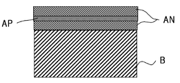
- FIG. 1 It is a schematic diagram which shows the structure of the transparent conductive film of this invention. It is a schematic diagram of a structure of an opposing target sputtering device used for manufacture of the transparent conductive film of this invention.
- the transparent substrate sheet used in the transparent conductive film of the present invention various polymer films and / or sheets (so-called plastic films and sheets) having good translucency can be used.
- the polymer constituting the sheet is not particularly limited.
- polyethylene polypropylene (PP), polyethylene terephthalate (PET), polycarbonate (PC), polyphenylene sulfide (PPS), polytetrafluoroethylene (PTFE)
- PET polypropylene
- PET polyethylene terephthalate
- PC polycarbonate
- PPS polyphenylene sulfide
- PTFE polytetrafluoroethylene
- TAC triacetyl cellulose
- PVC polyvinyl chloride
- PI polyimide
- PA polyamide
- the “transparent” base sheet means a sheet having a very high visible light transmittance, and the visible light transmittance at a wavelength of 550 nm is 85% or more, preferably 92% or more.
- the thickness of the base sheet is not particularly limited, but usually 5 to 250 ⁇ m is used.
- the conductive metal thin film contained in the transparent conductive film is composed of a very thin film generally called an ultrathin film so as not to impede the light transmittance, and Pd, Nd and / or Ni in the present invention is 0.5.
- the film thickness is preferably 5 to 30 nm, more preferably 6 to 20 nm.
- the film thickness is 30 nm or more, it is difficult to ensure high light transmission, and when the film thickness is 5 nm or less, the film formation approaches an island structure, and sheet resistance increases and light absorption occurs, thereby obtaining sufficient surface resistance. (Not less than 10 ⁇ / ⁇ ) and the transparency is lowered.
- the metal constituting the conductive metal thin film is silver doped with 0.5 to 10 wt% of Pd, Nd and / or Ni, the doping amount is more preferably 0.6 to 5%, and further 0.8 to 3%. preferable. If the dope amount exceeds 10 wt%, the sheet resistance increases. If the dope amount is less than 0.5 wt%, agglomeration is likely to occur and oxidation proceeds, which is not preferable. Specifically, for example, 1 wt% palladium-doped silver, 1 wt% nickel-doped silver, or the like can be used.
- the metal that is the dopant may be one of Pd (palladium), Nd (neodymium), and Ni (nickel), or a combination of two or more. Moreover, as long as the effect of this invention is not prevented, another kind of dopant can further be included. Examples of other types of dopants include copper (Cu), gold (Au), platinum (Pt), germanium (Ge), cerium (Ce), and gadolinium (Gd). Silver doped with Pd, Nd and / or Ni has a higher recrystallization temperature than pure silver and has improved corrosion resistance. Therefore, it is considered that the original high transparency and low resistance of silver are exhibited. Yes.
- the conductive metal film is obtained by depositing the above-mentioned different metal doped silver, but may contain other components as long as the effects of the present invention are not hindered.
- a nitride semiconductor thin film is formed above and below the conductive metal thin film.
- “upper” and “lower” of the metal thin film refer to the side closer to the base sheet when viewing the positional relationship between the base sheet and the metal thin film as “lower” and the side opposite to the base sheet as “upper”. Is.
- the nitride semiconductor thin film may have a structure in which one layer is formed above and below the conductive metal thin film (that is, a transparent conductive film having a three-layer structure including the conductive metal thin film).
- a structure in which two or more layers are laminated on the upper and lower sides of the conductive metal thin film may be used.
- a laminate having a three-layer structure is preferable.
- the nitride semiconductor thin film of the transparent conductive film of the present invention includes a nitride film of aluminum and / or an aluminum alloy.
- An example of such a nitride semiconductor thin film is an aluminum nitride film formed by reactive sputtering using nitrogen. This film can be obtained by using aluminum and / or an aluminum alloy as a sputtering film formation target and mixing Ar gas as a sputtering gas with a nitrogen gas having a flow rate ratio of 0.1 to 50%.
- the aluminum alloy used for the nitride semiconductor film may be a general alloy made of aluminum, Sn, Ti, or the like, and one or more selected from Nd, Ni, Ag, Cu, Sn, Pd, and Ti.
- An aluminum alloy to which a small amount of metal (0.1 to 10 wt%) is added may also be used.
- an aluminum alloy to which 0.1 to 10 wt% of Cu, Sn and / or Ti is added is preferable.
- As aluminum which is not an alloy it is preferable to use pure aluminum having a purity of 4N to 5N.
- the thickness of the nitride semiconductor film is 5 to 70 nm, preferably 10 to 65 nm, and more preferably 20 to 60 nm. Since the transmittance of the nitride semiconductor film is improved by light interference, the nitride semiconductor film has a film thickness region corresponding to the refractive index of the film, and the transmittance decreases if it is too thick or too thin. If the thickness of the nitride semiconductor film is less than 5 nm or more than 70 nm, the antireflection effect in the visible light region is reduced, and the transmittance is lowered, which is not preferable.
- the thickness (thickness excluding the base sheet) of the laminated structure of the conductive metal thin film and the nitride semiconductor thin film formed on the base sheet is 15 to 170 nm, more preferably 20 to 160 nm, and still more preferably. 30 to 150 nm.
- This film thickness range is derived from the optimum values of the film thickness of each of the conductive metal thin film and the nitride semiconductor thin film laminated structure. If the thickness is less than 15 nm, the sheet resistance value increases. This is not preferable because the rate decreases.
- the combination of the film thickness of the conductive metal thin film and the nitride semiconductor thin film can be appropriately selected in accordance with the use and desired characteristics within the above range.
- the nitride semiconductor thin film has a thickness of 20 to 50 nm and is electrically conductive.
- the conductive metal thin film is combined at 8 to 20 nm, a transparent conductive film having particularly suitable transparency and low resistance can be obtained.
- the transparent conductive film having a transmittance of 80% or more in the entire visible light region, and the electromagnetic wave shielding transparent conductive film further reducing the resistance value
- Various applications such as a transparent conductive film having heat ray shielding properties can be assumed.
- the transparent conductive film of the present invention has both a visible light transmittance of 85% to 99% and a sheet resistance value of 0.1 to 10 ⁇ / ⁇ , both of a very high level of visible light transmittance and a sheet resistance value.
- the visible light transmittance as used in this specification has shown the value of the transmittance
- the sheet resistance value indicates a resistance value ( ⁇ / ⁇ ) measured by the four-probe method.
- FIG. 1 A schematic diagram of the transparent conductive film of the present invention is shown in FIG.
- the transparent conductive film shown in FIG. 1 is laminated on a plastic substrate sheet (B).
- a high refractive index (refractive index 2) is formed on both upper and lower sides of a conductive metal thin film (AP) which is a palladium-doped silver thin film.
- AP conductive metal thin film
- an undercoat layer is provided on the base sheet (B) to form a protective film for the base sheet, and a transparent conductive film laminate is formed thereon.
- another top coat layer may be provided on the uppermost layer of the transparent conductive laminate to provide a characteristic improvement or a protective function.
- the transparent heat insulating sheet of the present invention is generally produced by sequentially forming a nitride semiconductor thin film and a conductive metal thin film on a base sheet.
- the method for forming the nitride semiconductor thin film and the conductive metal thin film include a physical vapor deposition (PVD) method such as a vacuum vapor deposition method and a sputtering method, and a chemical vapor deposition (CVD) method.
- PVD physical vapor deposition
- CVD chemical vapor deposition
- N-MHVS method New Magnetic Hollow-cathode V-type sputtering method
- an excellent conductive metal thin film or nitride semiconductor thin film is used. Can be formed stably.
- the N-MHVS method is described in detail in Japanese Patent No. 4473852, but the opposite target sputtering method (FTS method), which is a sputtering method capable of forming a film at a lower temperature and with lower damage than a normal magnetron sputtering method, is highly effective. This is an improved method.
- FTS method opposite target sputtering method
- the N-MHVS method enables film formation with extremely low energy (sputtering voltage of -300V or less) by generating high-density plasma with opposed double magnetic poles, compared to the general magnetron sputtering method.
- a good quality thin film having a uniform composition and few defects can be obtained in a low temperature process, and the conductivity of the metal thin film and the smoothness of the film surface can be improved.
- a nitride semiconductor film formed by reactive sputtering by the N-MHVS method should have a sufficient reactivity under high-density plasma, and should form a metal nitride thin film with a smooth surface and low absorption. Therefore, a laminated film can be obtained without damaging the surface of the conductive metal thin film or nitride semiconductor thin film.
- N-MHV sputtering apparatus which is a specific apparatus of the N-MHVS method, will be described with reference to FIG. 2 includes a target holder 11a, 11b having a pair of targets 10a, 10b arranged at the tip, a vacuum chamber 2, a power supply 3 for supplying sputtering power, a substrate holder 4, an exhaust device 5, and a gas supply device 6. I have.
- the pair of targets 10a and 10b is made of, for example, aluminum Al (purity 5N).
- the targets 10a and 10b are disposed opposite to each other in the vacuum chamber 2, and facing surfaces (surfaces to be sputtered) 10a 'and 10b' are disposed at a predetermined interval.
- the target holders 11a and 11b support and fix the targets 10a and 10b through the backing plates 12a and 12b, respectively.
- the target holders 11a and 11b are inserted through an insulating plate (not shown) so that the tip side is positioned inside the vacuum chamber 2. Attached to the vacuum chamber 2.
- the pair of targets 10a and 10b is placed on the film-forming surface B ′ of the substrate B in which both opposing surfaces 10a ′ and 10b ′ are fixed by the substrate holder 4 in the vacuum chamber 2 by the target holders 11a and 11b.
- the inclination angle can be set to 5 °.
- the targets 10a 'and 10b' in which the opposing surfaces 10a 'and 10b' are substantially V-shaped are generally referred to as "V-type opposing targets".
- Inter-target magnetic field generating means 20a and 20b are disposed on the outer surfaces of the backing plates 12a and 12b that fix the targets 10a and 10b (surfaces opposite to the surfaces on which the targets 10a and 10b are fixed). .
- the inter-target magnetic field generating means is a means for generating (forming) a magnetic field space (inter-target magnetic field space) between the targets 10a and 10b, and is composed of, for example, a permanent magnet.
- the inter-target magnetic field generating means 20a, 20b is made of a ferromagnetic material such as a neodymium (eg, neodymium, iron, boron) magnet or an alnico magnet.
- One inter-target magnetic field generating means 20a is arranged so that the N pole faces the outer surface of one target 10a in order to generate a magnetic field in a direction perpendicular to the opposing surface 10a ′, and the other.
- the inter-target magnetic field generating means 20b is arranged so that the south pole faces the outer surface of the other target 10b in order to generate a magnetic field in a direction perpendicular to the facing surface 10b ′.
- an inter-target magnetic field space K is formed between the opposing surfaces 10a 'and 10b' of the targets 10a and 10b so that the lines of magnetic force are directed from the opposing surface 10a 'to the opposing surface 10b'.
- the auxiliary magnetic field generating means 30a and 30b are formed of permanent magnets similarly to the inter-target magnetic field generating means 20a and 20b, and are formed in a rectangular tube shape that can be fitted (externally fitted) along the outer periphery of the target holders 11a and 11b. Has been.
- the auxiliary magnetic field generation means 30a and 30b are arranged so that the magnetic poles are fitted in the same direction as the inter-target magnetic field generation means 20a and 20b and are fitted on the outer circumferences of the front ends of the target holders 11a and 11b.
- the power supply 3 for sputter power supply is a power supply capable of applying DC constant power, and supplies the sputter power with the vacuum chamber 2 at the ground potential (earth potential) as an anode and the targets 10a and 10b as cathodes. .
- the substrate holder 4 supports the base sheet B and is disposed so that the film formation surface B ′ of the base sheet B faces the space K formed between the opposing faces 10a ′ and 10b ′ by the targets 10a and 10b. .
- the vacuum chamber 2 is connected to an exhaust device 5 and a gas supply device 6 for discharge gas.
- the gas supply device 6 is disposed in the vicinity of the targets 10a and 10b, respectively.
- Sputter gas introduction supply ports 6 ′ and 6 ′ for supplying a sputtering gas which is an inert gas, and a reaction for supplying a reactive gas.
- Gas supply ports 6 ′′, 6 ′′ are included.
- both opposing surfaces 10a ′, 20a, 20b and inter-target magnetic field generating means 20a, 20b on the back side of the target and auxiliary magnetic field generating means 30a, 30b arranged along the periphery of the target are surrounded by double magnetic poles.
- High density plasma can be formed in the space K formed between 10b '.
- the sputtering gas and the reactive gas are supplied from the sputtering gas supply ports 6 ′ and 6 ′ arranged on the opposite surface of the substrate of the counter target and the reactive gas supply ports 6 ′′ and 6 ′′ arranged on both sides in the vicinity of the substrate. Supplied respectively.
- the target material metal
- the formation of the ceramic thin film by plasma reaction such as oxidation and nitridation involves active sputtered particles near the substrate.
- a reaction thin film is formed by reacting with the reaction gas. For this reason, the target surface is not exposed to a plasma reaction such as oxidation or nitridation, and has a structure in which stable reactive sputtering is sustained.
- the above apparatus can greatly reduce the sputtering voltage in a low pressure state due to the strong inter-target magnetic field space generated by the double magnetic pole of the target magnetic pole and the auxiliary magnetic pole. it can.
- the powerful double magnetic poles can more effectively exhibit the confinement effect of plasma and the confinement effect of charged particles such as secondary electrons, and enables film formation at low temperature and low damage.
- a metal material to be oxynitride is used for the targets 10a and 10b, and the base sheet B to be formed is set on the substrate holder 4. Then, the vacuum chamber 2 is evacuated to a predetermined degree of vacuum, a predetermined amount of sputtering gas (Ar gas) and reaction gas (N 2 ) is added, and sputtering is performed with a predetermined sputtering power and sputtering time. By this sputtering, a nitride semiconductor thin film having a predetermined thickness is formed on the base sheet B.
- sputtering is performed by supplying only the sputtering gas (Ar gas) without supplying the reactive gas.
- the film formation step can be performed without heating the substrate sheet B or the vacuum chamber 2 (at room temperature), and a good thin film can be obtained by performing the film formation without heating the substrate.
- room temperature about 20-50 ° C
- low damage film formation is possible, and a more uniform thin film with fewer defects can be obtained, achieving both transparency and low resistance.
- a transparent conductive film can be obtained.
- the transparent conductive film of the Example and comparative example of this invention was created in the following procedure.
- a PET film of 100 mm ⁇ 100 mm ⁇ 100 ⁇ m (visible light transmittance of 92% at a wavelength of 500 nm) was degreased, washed and dried.
- a predetermined thin film was formed on the film by the N-MHV sputtering apparatus shown in FIG.
- Various thin films were formed under the following conditions.
- AlN film Aluminum Al (purity 5N), 125 mm ⁇ 300 mm was used as a target. The Al was placed on a target holder, and the PET film was set on a substrate holder. Subsequently, after evacuating the inside of the vacuum chamber to 10 ⁇ 5 Pa or less, Ar gas as a sputtering gas and N 2 gas as a reaction gas are sequentially supplied, and Ar gas at 0.3 Pa and N 2 gas is supplied inside the vacuum chamber. The gas was 0.15 Pa. The sputtering power was 500 W, the sputtering time was adjusted according to the desired film thickness, and an AlN thin film having a predetermined film thickness was obtained.
- Ar gas as a sputtering gas and N 2 gas as a reaction gas are sequentially supplied, and Ar gas at 0.3 Pa and N 2 gas is supplied inside the vacuum chamber.
- the gas was 0.15 Pa.
- the sputtering power was 500 W, the sputtering time was adjusted according to the desired film thickness, and
- the sputtering power was 500 W
- the sputtering time was adjusted according to the desired film thickness
- an AgPd thin film having a predetermined film thickness was obtained.
- it formed into a film like the above except using pure Ag as a target.
- Example 1 AlN / AgPd / AlN laminated film A laminated film of AlN 20 nm / AgPd 8 nm / AlN 20 nm was prepared based on the above film forming conditions. The film formation (sputtering) time of the AlN 20 nm thin film was 4 minutes, and the film formation (sputtering) time of the AgPd 8 nm thin film was 40 seconds.
- Example 2 A laminated film was prepared in the same manner as in Example 1 except that the AgPd film was changed to 10 nm (sputtering time 50 seconds).
- Example 3 A laminated film was prepared in the same manner as in Example 1 except that the AlN film was changed to 30 nm (sputtering time 6 minutes).
- Example 4 A laminated film was prepared in the same manner as in Example 1 except that the AlN film was 30 nm (sputtering time 6 minutes) and the AgPd film was 10 nm (sputtering time 50 seconds).
- Example 5 A laminated film was prepared in the same manner as in Example 1 except that the AlN film was 30 nm (sputtering time 6 minutes) and the AgPd film was 12 nm (sputtering time 60 seconds).
- Example 6 A laminated film was prepared in the same manner as in Example 1 except that the AlN film was 40 nm (sputtering time 8 minutes).
- Example 7 A laminated film was prepared in the same manner as in Example 1 except that the AlN film was 40 nm (sputtering time 8 minutes) and the AgPd film was 10 nm (sputtering time 50 seconds).
- Example 8 A laminated film was prepared in the same manner as in Example 1 except that the AlN film was 40 nm (sputtering time 8 minutes) and the AgPd film was 12 nm (sputtering time 60 seconds).
- Example 9 A laminated film was prepared in the same manner as in Example 1 except that the AlN film was 40 nm (sputtering time 8 minutes) and the AgPd film was 14 nm (sputtering time 70 seconds).
- Example 10 A laminated film was prepared in the same manner as in Example 1 except that the AlN film was 40 nm (sputtering time 8 minutes) and the AgPd film was 16 nm (sputtering time 80 seconds).
- Example 11 A laminated film was prepared in the same manner as in Example 1 except that the AlN film was 40 nm (sputtering time 8 minutes) and the AgPd film was 18 nm (sputtering time 90 seconds).
- Example 12 A laminated film was prepared in the same manner as in Example 1 except that the AlN film was 40 nm (sputtering time 8 minutes) and the AgPd film was 20 nm (sputtering time 100 seconds).
- Example 13 A laminated film was prepared in the same manner as in Example 1 except that the AlN film was 50 nm (sputtering time was 10 minutes).
- Example 14 A laminated film was prepared in the same manner as in Example 1 except that the AlN film was 50 nm (sputtering time 10 minutes) and the AgPd film was 10 nm (sputtering time 50 seconds).
- Example 15 A laminated film was prepared in the same manner as in Example 1 except that the AlN film was 50 nm (sputtering time 10 minutes) and the AgPd film was 12 nm (sputtering time 60 seconds).
- Example 16 A laminated film was prepared in the same manner as in Example 1 except that the AlN film was 50 nm (sputtering time 10 minutes) and the AgPd film was 14 nm (sputtering time 70 seconds).
- Comparative Example 2 A laminated film was prepared in the same manner as in Comparative Example 1 except that the pure Ag film was changed to 10 nm (sputtering time 50 seconds).
- Comparative Example 3 A laminated film was prepared in the same manner as in Comparative Example 1 except that the pure Ag film was 12 nm (sputtering time 60 seconds).
- Comparative Example 4 A laminated film was prepared in the same manner as in Comparative Example 1 except that the pure Ag film was changed to 14 nm (sputtering time 70 seconds).
- Comparative Example 5 A laminated film was prepared in the same manner as in Comparative Example 1 except that the pure Ag film was 16 nm (sputtering time 80 seconds).
- Comparative Example 6 A laminated film was prepared in the same manner as in Comparative Example 1 except that the pure Ag film was 18 nm (sputtering time 90 seconds).
- the transmittance (%) and sheet resistance value ( ⁇ / ⁇ ) at a wavelength of 500 nm of the laminated films (transparent conductive films) obtained in Examples and Comparative Examples are shown in the following table.
- the transmittance was measured using a spectrophotometer HUS-100S manufactured by Asahi Spectroscopy Co., Ltd., with reference to each substrate.
- the sheet resistance value was measured by a four probe method using Loresta AX (MCP-T370) manufactured by Mitsubishi Chemical Corporation.
Landscapes
- Chemical & Material Sciences (AREA)
- Engineering & Computer Science (AREA)
- Physics & Mathematics (AREA)
- Power Engineering (AREA)
- Mechanical Engineering (AREA)
- Metallurgy (AREA)
- Organic Chemistry (AREA)
- Materials Engineering (AREA)
- Chemical Kinetics & Catalysis (AREA)
- Condensed Matter Physics & Semiconductors (AREA)
- Electromagnetism (AREA)
- General Physics & Mathematics (AREA)
- Computer Hardware Design (AREA)
- Microelectronics & Electronic Packaging (AREA)
- Manufacturing & Machinery (AREA)
- Physical Vapour Deposition (AREA)
- Laminated Bodies (AREA)
- Non-Insulated Conductors (AREA)
- Manufacturing Of Electric Cables (AREA)
Abstract
La présente invention concerne : un film conducteur transparent qui a simultanément un facteur de transmission élevé et une résistance superficielle faible, c'est-à-dire un facteur de transmission de lumière visible de 85 % ou plus et une résistance superficielle de 10 Ω/□ ou moins, lesdits facteurs de transmission de lumière visible et résistance superficielle étant aux niveaux les plus élevés pour des films conducteurs transparents ; et un procédé de production pour produire le film conducteur transparent par un procédé pratique et industrialisable.
Un film conducteur transparent est obtenu en produisant une structure multicouche, qui comprend une couche mince de métal conducteur et des couches minces de semi-conducteur de nitrure qui sont stratifiées sur les surfaces supérieure et inférieure de la couche mince de métal conducteur, sur une feuille de base transparente. Ce film conducteur transparent est caractérisé en ce que : la couche mince de métal conducteur est une couche mince formée d'argent qui est dopé avec Pd, Nd et/ou Ni dans une quantité de 0,5 à 10 % en poids ; et les couches minces de semi-conducteur de nitrure sont des couches minces d'un nitrure d'aluminium et/ou un d'alliage d'aluminium.
Applications Claiming Priority (2)
| Application Number | Priority Date | Filing Date | Title |
|---|---|---|---|
| JP2012169184A JP5938290B2 (ja) | 2012-07-31 | 2012-07-31 | 透明導電膜及びその製造方法 |
| JP2012-169184 | 2012-07-31 |
Publications (1)
| Publication Number | Publication Date |
|---|---|
| WO2014021325A1 true WO2014021325A1 (fr) | 2014-02-06 |
Family
ID=50027998
Family Applications (1)
| Application Number | Title | Priority Date | Filing Date |
|---|---|---|---|
| PCT/JP2013/070618 WO2014021325A1 (fr) | 2012-07-31 | 2013-07-30 | Film conducteur transparent et procédé pour produire celui-ci |
Country Status (3)
| Country | Link |
|---|---|
| JP (1) | JP5938290B2 (fr) |
| TW (1) | TWI630658B (fr) |
| WO (1) | WO2014021325A1 (fr) |
Cited By (3)
| Publication number | Priority date | Publication date | Assignee | Title |
|---|---|---|---|---|
| WO2015179834A1 (fr) * | 2014-05-23 | 2015-11-26 | The Regents Of The University Of Michigan | Films ultra-minces de métal noble dopé pour applications optoélectroniques et photoniques |
| CN113748374A (zh) * | 2019-06-28 | 2021-12-03 | 日东电工株式会社 | 带粘合剂层的偏振膜及液晶面板 |
| CN114622162A (zh) * | 2022-03-14 | 2022-06-14 | 南京邮电大学 | 一种耐高温透明导电复合薄膜及其制备方法和应用 |
Families Citing this family (4)
| Publication number | Priority date | Publication date | Assignee | Title |
|---|---|---|---|---|
| JP6366221B2 (ja) * | 2012-09-21 | 2018-08-01 | コニカミノルタ株式会社 | 透明電極、及び電子デバイス |
| CN104269221A (zh) * | 2014-08-29 | 2015-01-07 | 上海蓝沛新材料科技股份有限公司 | 一种利用含钯化合物的墨水制备透明导电膜的方法 |
| JP2016191967A (ja) * | 2015-03-30 | 2016-11-10 | 株式会社神戸製鋼所 | 窒素含有Cu合金膜、積層膜、およびこれらの製造方法、ならびにCu合金スパッタリングターゲット |
| CN113913775A (zh) * | 2021-09-30 | 2022-01-11 | 浙江师范大学 | 对向靶磁控溅射无损伤薄膜沉积系统 |
Citations (6)
| Publication number | Priority date | Publication date | Assignee | Title |
|---|---|---|---|---|
| JPS63205609A (ja) * | 1987-02-20 | 1988-08-25 | Unitika Ltd | 熱線反射膜 |
| JPH07105740A (ja) * | 1993-10-08 | 1995-04-21 | Mitsui Toatsu Chem Inc | 透明導電性フィルム |
| JP2001164382A (ja) * | 1999-12-03 | 2001-06-19 | Osaka Prefecture | 導電性光選択透過シート |
| JP2004047216A (ja) * | 2002-07-10 | 2004-02-12 | Central Glass Co Ltd | 透明導電膜 |
| JP2007250430A (ja) * | 2006-03-17 | 2007-09-27 | Sumitomo Metal Mining Co Ltd | 透明導電膜、およびこれを用いた透明導電性フィルム |
| JP2008184625A (ja) * | 2007-01-26 | 2008-08-14 | Osaka Vacuum Ltd | スパッタ方法及びスパッタ装置 |
-
2012
- 2012-07-31 JP JP2012169184A patent/JP5938290B2/ja not_active Expired - Fee Related
-
2013
- 2013-07-30 WO PCT/JP2013/070618 patent/WO2014021325A1/fr active Application Filing
- 2013-07-31 TW TW102127409A patent/TWI630658B/zh not_active IP Right Cessation
Patent Citations (6)
| Publication number | Priority date | Publication date | Assignee | Title |
|---|---|---|---|---|
| JPS63205609A (ja) * | 1987-02-20 | 1988-08-25 | Unitika Ltd | 熱線反射膜 |
| JPH07105740A (ja) * | 1993-10-08 | 1995-04-21 | Mitsui Toatsu Chem Inc | 透明導電性フィルム |
| JP2001164382A (ja) * | 1999-12-03 | 2001-06-19 | Osaka Prefecture | 導電性光選択透過シート |
| JP2004047216A (ja) * | 2002-07-10 | 2004-02-12 | Central Glass Co Ltd | 透明導電膜 |
| JP2007250430A (ja) * | 2006-03-17 | 2007-09-27 | Sumitomo Metal Mining Co Ltd | 透明導電膜、およびこれを用いた透明導電性フィルム |
| JP2008184625A (ja) * | 2007-01-26 | 2008-08-14 | Osaka Vacuum Ltd | スパッタ方法及びスパッタ装置 |
Cited By (4)
| Publication number | Priority date | Publication date | Assignee | Title |
|---|---|---|---|---|
| WO2015179834A1 (fr) * | 2014-05-23 | 2015-11-26 | The Regents Of The University Of Michigan | Films ultra-minces de métal noble dopé pour applications optoélectroniques et photoniques |
| US10475548B2 (en) | 2014-05-23 | 2019-11-12 | The Regents Of The University Of Michigan | Ultra-thin doped noble metal films for optoelectronics and photonics applications |
| CN113748374A (zh) * | 2019-06-28 | 2021-12-03 | 日东电工株式会社 | 带粘合剂层的偏振膜及液晶面板 |
| CN114622162A (zh) * | 2022-03-14 | 2022-06-14 | 南京邮电大学 | 一种耐高温透明导电复合薄膜及其制备方法和应用 |
Also Published As
| Publication number | Publication date |
|---|---|
| TWI630658B (zh) | 2018-07-21 |
| TW201411724A (zh) | 2014-03-16 |
| JP5938290B2 (ja) | 2016-06-22 |
| JP2014028986A (ja) | 2014-02-13 |
Similar Documents
| Publication | Publication Date | Title |
|---|---|---|
| WO2014021325A1 (fr) | Film conducteur transparent et procédé pour produire celui-ci | |
| KR101344500B1 (ko) | 반사 방지막의 성막 방법 및 반사 방지막 | |
| CN103258966B (zh) | 用于有机发光装置的反射阳极电极及其制造方法 | |
| JP2009199986A (ja) | 酸化亜鉛系透明導電膜積層体と透明導電性基板およびデバイス | |
| TW200918479A (en) | Conductor layer manufacturing method | |
| JP2017122282A (ja) | 透明導電性フィルムの製造方法 | |
| CN102066601B (zh) | 触摸面板的制造方法和成膜装置 | |
| JP2009293097A (ja) | スパッタリング複合ターゲット、これを用いた透明導電膜の製造方法及び透明導電膜付基材 | |
| WO2013099084A1 (fr) | Procédé de fabrication d'un élément électroluminescent organique | |
| JP5447240B2 (ja) | マグネトロンスパッタリング装置および透明導電膜の製造方法 | |
| JP2014218042A (ja) | 透明断熱シート及びその製造方法 | |
| CN103924191A (zh) | 在基片上镀制ito薄膜的方法 | |
| JP2017193755A (ja) | 透明導電膜の製造方法、及び透明導電膜 | |
| JP2017008380A (ja) | 透明電極付き基板およびその製造方法 | |
| JPWO2009028372A1 (ja) | 透明導電膜の形成方法 | |
| CN114231903A (zh) | 一种氧化铌/银纳米线双层结构柔性透明导电薄膜及其制备方法 | |
| JPH0273963A (ja) | 低温基体への薄膜形成方法 | |
| JP6484098B2 (ja) | 透明導電フィルムおよび表示デバイス、並びに、透明導電フィルムの製造方法および表示デバイスの製造方法 | |
| JP2014047400A (ja) | フラットパネルディスプレイの半透過電極用Ag合金膜、およびフラットパネルディスプレイ用半透過電極 | |
| JP2013202893A (ja) | 透明断熱シート | |
| JP7478721B2 (ja) | 透明電極付き基板の製造方法 | |
| JP2012179762A (ja) | 透明ガスバリアフィルム、透明ガスバリアフィルムの製造方法、有機エレクトロルミネッセンス素子、太陽電池および薄膜電池 | |
| JP2004247060A (ja) | 透明導電性酸化物複合体とこれを用いた太陽電池および表示装置 | |
| TW201326443A (zh) | 透明導電膜及其製造方法 | |
| JP2000243160A (ja) | 透明導電積層体の製造方法 |
Legal Events
| Date | Code | Title | Description |
|---|---|---|---|
| 121 | Ep: the epo has been informed by wipo that ep was designated in this application |
Ref document number: 13825821 Country of ref document: EP Kind code of ref document: A1 |
|
| NENP | Non-entry into the national phase |
Ref country code: DE |
|
| 122 | Ep: pct application non-entry in european phase |
Ref document number: 13825821 Country of ref document: EP Kind code of ref document: A1 |