JP5938290B2 - 透明導電膜及びその製造方法 - Google Patents
透明導電膜及びその製造方法 Download PDFInfo
- Publication number
- JP5938290B2 JP5938290B2 JP2012169184A JP2012169184A JP5938290B2 JP 5938290 B2 JP5938290 B2 JP 5938290B2 JP 2012169184 A JP2012169184 A JP 2012169184A JP 2012169184 A JP2012169184 A JP 2012169184A JP 5938290 B2 JP5938290 B2 JP 5938290B2
- Authority
- JP
- Japan
- Prior art keywords
- film
- thin film
- transparent conductive
- sputtering
- conductive film
- Prior art date
- Legal status (The legal status is an assumption and is not a legal conclusion. Google has not performed a legal analysis and makes no representation as to the accuracy of the status listed.)
- Expired - Fee Related
Links
- 238000004519 manufacturing process Methods 0.000 title claims description 15
- 239000010408 film Substances 0.000 claims description 202
- 239000010409 thin film Substances 0.000 claims description 98
- 238000004544 sputter deposition Methods 0.000 claims description 80
- 229910052751 metal Inorganic materials 0.000 claims description 62
- 239000002184 metal Substances 0.000 claims description 62
- 150000004767 nitrides Chemical class 0.000 claims description 38
- 238000002834 transmittance Methods 0.000 claims description 38
- 230000005291 magnetic effect Effects 0.000 claims description 36
- 239000007789 gas Substances 0.000 claims description 35
- 239000004065 semiconductor Substances 0.000 claims description 34
- 239000000758 substrate Substances 0.000 claims description 25
- BQCADISMDOOEFD-UHFFFAOYSA-N Silver Chemical compound [Ag] BQCADISMDOOEFD-UHFFFAOYSA-N 0.000 claims description 22
- 239000004332 silver Substances 0.000 claims description 22
- 229910052709 silver Inorganic materials 0.000 claims description 21
- 229910052779 Neodymium Inorganic materials 0.000 claims description 11
- 229910052763 palladium Inorganic materials 0.000 claims description 11
- 229910052782 aluminium Inorganic materials 0.000 claims description 10
- XAGFODPZIPBFFR-UHFFFAOYSA-N aluminium Chemical compound [Al] XAGFODPZIPBFFR-UHFFFAOYSA-N 0.000 claims description 10
- 229910052718 tin Inorganic materials 0.000 claims description 8
- 229910052802 copper Inorganic materials 0.000 claims description 7
- 238000010438 heat treatment Methods 0.000 claims description 6
- IJGRMHOSHXDMSA-UHFFFAOYSA-N Atomic nitrogen Chemical compound N#N IJGRMHOSHXDMSA-UHFFFAOYSA-N 0.000 claims description 5
- PMHQVHHXPFUNSP-UHFFFAOYSA-M copper(1+);methylsulfanylmethane;bromide Chemical compound Br[Cu].CSC PMHQVHHXPFUNSP-UHFFFAOYSA-M 0.000 claims description 5
- 239000011261 inert gas Substances 0.000 claims description 5
- 229910001873 dinitrogen Inorganic materials 0.000 claims description 3
- 229910052759 nickel Inorganic materials 0.000 claims description 3
- 238000000034 method Methods 0.000 description 27
- 230000015572 biosynthetic process Effects 0.000 description 15
- KDLHZDBZIXYQEI-UHFFFAOYSA-N palladium Substances [Pd] KDLHZDBZIXYQEI-UHFFFAOYSA-N 0.000 description 15
- 230000000052 comparative effect Effects 0.000 description 14
- PXHVJJICTQNCMI-UHFFFAOYSA-N nickel Substances [Ni] PXHVJJICTQNCMI-UHFFFAOYSA-N 0.000 description 10
- 239000010949 copper Substances 0.000 description 8
- 230000000694 effects Effects 0.000 description 8
- 229910000838 Al alloy Inorganic materials 0.000 description 7
- 229910003437 indium oxide Inorganic materials 0.000 description 7
- PJXISJQVUVHSOJ-UHFFFAOYSA-N indium(iii) oxide Chemical compound [O-2].[O-2].[O-2].[In+3].[In+3] PJXISJQVUVHSOJ-UHFFFAOYSA-N 0.000 description 7
- 239000011135 tin Substances 0.000 description 6
- 239000010936 titanium Substances 0.000 description 5
- 239000000919 ceramic Substances 0.000 description 4
- 238000006243 chemical reaction Methods 0.000 description 4
- -1 polyethylene Polymers 0.000 description 4
- 239000012495 reaction gas Substances 0.000 description 4
- 238000005546 reactive sputtering Methods 0.000 description 4
- 229920002799 BoPET Polymers 0.000 description 3
- 230000007547 defect Effects 0.000 description 3
- 238000010586 diagram Methods 0.000 description 3
- 239000002019 doping agent Substances 0.000 description 3
- 239000010931 gold Substances 0.000 description 3
- QEFYFXOXNSNQGX-UHFFFAOYSA-N neodymium atom Chemical compound [Nd] QEFYFXOXNSNQGX-UHFFFAOYSA-N 0.000 description 3
- 230000003647 oxidation Effects 0.000 description 3
- 238000007254 oxidation reaction Methods 0.000 description 3
- 238000005240 physical vapour deposition Methods 0.000 description 3
- BASFCYQUMIYNBI-UHFFFAOYSA-N platinum Chemical compound [Pt] BASFCYQUMIYNBI-UHFFFAOYSA-N 0.000 description 3
- 229920002284 Cellulose triacetate Polymers 0.000 description 2
- XEEYBQQBJWHFJM-UHFFFAOYSA-N Iron Chemical compound [Fe] XEEYBQQBJWHFJM-UHFFFAOYSA-N 0.000 description 2
- 239000004952 Polyamide Substances 0.000 description 2
- 239000004698 Polyethylene Substances 0.000 description 2
- 239000004642 Polyimide Substances 0.000 description 2
- 239000004734 Polyphenylene sulfide Substances 0.000 description 2
- 239000004743 Polypropylene Substances 0.000 description 2
- NNLVGZFZQQXQNW-ADJNRHBOSA-N [(2r,3r,4s,5r,6s)-4,5-diacetyloxy-3-[(2s,3r,4s,5r,6r)-3,4,5-triacetyloxy-6-(acetyloxymethyl)oxan-2-yl]oxy-6-[(2r,3r,4s,5r,6s)-4,5,6-triacetyloxy-2-(acetyloxymethyl)oxan-3-yl]oxyoxan-2-yl]methyl acetate Chemical compound O([C@@H]1O[C@@H]([C@H]([C@H](OC(C)=O)[C@H]1OC(C)=O)O[C@H]1[C@@H]([C@@H](OC(C)=O)[C@H](OC(C)=O)[C@@H](COC(C)=O)O1)OC(C)=O)COC(=O)C)[C@@H]1[C@@H](COC(C)=O)O[C@@H](OC(C)=O)[C@H](OC(C)=O)[C@H]1OC(C)=O NNLVGZFZQQXQNW-ADJNRHBOSA-N 0.000 description 2
- 238000005054 agglomeration Methods 0.000 description 2
- 230000002776 aggregation Effects 0.000 description 2
- 229910045601 alloy Inorganic materials 0.000 description 2
- 239000000956 alloy Substances 0.000 description 2
- 238000005229 chemical vapour deposition Methods 0.000 description 2
- 230000007423 decrease Effects 0.000 description 2
- PCHJSUWPFVWCPO-UHFFFAOYSA-N gold Chemical compound [Au] PCHJSUWPFVWCPO-UHFFFAOYSA-N 0.000 description 2
- 229910052737 gold Inorganic materials 0.000 description 2
- 230000006872 improvement Effects 0.000 description 2
- 238000009413 insulation Methods 0.000 description 2
- 238000001755 magnetron sputter deposition Methods 0.000 description 2
- 239000000463 material Substances 0.000 description 2
- 229910052757 nitrogen Inorganic materials 0.000 description 2
- 239000002245 particle Substances 0.000 description 2
- 239000004033 plastic Substances 0.000 description 2
- 229920003023 plastic Polymers 0.000 description 2
- 239000002985 plastic film Substances 0.000 description 2
- 229920002647 polyamide Polymers 0.000 description 2
- 229920000573 polyethylene Polymers 0.000 description 2
- 229920000139 polyethylene terephthalate Polymers 0.000 description 2
- 239000005020 polyethylene terephthalate Substances 0.000 description 2
- 229920001721 polyimide Polymers 0.000 description 2
- 229920000069 polyphenylene sulfide Polymers 0.000 description 2
- 229920001155 polypropylene Polymers 0.000 description 2
- 229920001343 polytetrafluoroethylene Polymers 0.000 description 2
- 239000004810 polytetrafluoroethylene Substances 0.000 description 2
- 239000000523 sample Substances 0.000 description 2
- 229910001923 silver oxide Inorganic materials 0.000 description 2
- 229910052719 titanium Inorganic materials 0.000 description 2
- ZOXJGFHDIHLPTG-UHFFFAOYSA-N Boron Chemical compound [B] ZOXJGFHDIHLPTG-UHFFFAOYSA-N 0.000 description 1
- 229910052684 Cerium Inorganic materials 0.000 description 1
- RYGMFSIKBFXOCR-UHFFFAOYSA-N Copper Chemical compound [Cu] RYGMFSIKBFXOCR-UHFFFAOYSA-N 0.000 description 1
- PXGOKWXKJXAPGV-UHFFFAOYSA-N Fluorine Chemical compound FF PXGOKWXKJXAPGV-UHFFFAOYSA-N 0.000 description 1
- 229910052688 Gadolinium Inorganic materials 0.000 description 1
- GYHNNYVSQQEPJS-UHFFFAOYSA-N Gallium Chemical compound [Ga] GYHNNYVSQQEPJS-UHFFFAOYSA-N 0.000 description 1
- 229910052774 Proactinium Inorganic materials 0.000 description 1
- 229910006404 SnO 2 Inorganic materials 0.000 description 1
- ATJFFYVFTNAWJD-UHFFFAOYSA-N Tin Chemical compound [Sn] ATJFFYVFTNAWJD-UHFFFAOYSA-N 0.000 description 1
- XLOMVQKBTHCTTD-UHFFFAOYSA-N Zinc monoxide Chemical compound [Zn]=O XLOMVQKBTHCTTD-UHFFFAOYSA-N 0.000 description 1
- 238000010521 absorption reaction Methods 0.000 description 1
- 229910000828 alnico Inorganic materials 0.000 description 1
- 229910052787 antimony Inorganic materials 0.000 description 1
- WATWJIUSRGPENY-UHFFFAOYSA-N antimony atom Chemical compound [Sb] WATWJIUSRGPENY-UHFFFAOYSA-N 0.000 description 1
- 238000013459 approach Methods 0.000 description 1
- 230000005540 biological transmission Effects 0.000 description 1
- 229910052796 boron Inorganic materials 0.000 description 1
- GWXLDORMOJMVQZ-UHFFFAOYSA-N cerium Chemical compound [Ce] GWXLDORMOJMVQZ-UHFFFAOYSA-N 0.000 description 1
- 230000007797 corrosion Effects 0.000 description 1
- 238000005260 corrosion Methods 0.000 description 1
- 238000000151 deposition Methods 0.000 description 1
- 239000003302 ferromagnetic material Substances 0.000 description 1
- 239000011737 fluorine Substances 0.000 description 1
- 229910052731 fluorine Inorganic materials 0.000 description 1
- UIWYJDYFSGRHKR-UHFFFAOYSA-N gadolinium atom Chemical compound [Gd] UIWYJDYFSGRHKR-UHFFFAOYSA-N 0.000 description 1
- 229910052733 gallium Inorganic materials 0.000 description 1
- 229910052732 germanium Inorganic materials 0.000 description 1
- GNPVGFCGXDBREM-UHFFFAOYSA-N germanium atom Chemical compound [Ge] GNPVGFCGXDBREM-UHFFFAOYSA-N 0.000 description 1
- 238000007733 ion plating Methods 0.000 description 1
- 229910052742 iron Inorganic materials 0.000 description 1
- 238000000608 laser ablation Methods 0.000 description 1
- 230000031700 light absorption Effects 0.000 description 1
- 239000004973 liquid crystal related substance Substances 0.000 description 1
- 239000012528 membrane Substances 0.000 description 1
- 239000007769 metal material Substances 0.000 description 1
- 150000002739 metals Chemical class 0.000 description 1
- 239000000203 mixture Substances 0.000 description 1
- 230000035699 permeability Effects 0.000 description 1
- 230000000704 physical effect Effects 0.000 description 1
- 229920006255 plastic film Polymers 0.000 description 1
- 229910052697 platinum Inorganic materials 0.000 description 1
- 239000004417 polycarbonate Substances 0.000 description 1
- 229920000515 polycarbonate Polymers 0.000 description 1
- 229920000642 polymer Polymers 0.000 description 1
- 229920006254 polymer film Polymers 0.000 description 1
- 239000004800 polyvinyl chloride Substances 0.000 description 1
- 230000008569 process Effects 0.000 description 1
- 230000001681 protective effect Effects 0.000 description 1
- 230000009993 protective function Effects 0.000 description 1
- 230000009257 reactivity Effects 0.000 description 1
- 238000001953 recrystallisation Methods 0.000 description 1
- 239000010944 silver (metal) Substances 0.000 description 1
- 239000000126 substance Substances 0.000 description 1
- 230000002459 sustained effect Effects 0.000 description 1
- 239000013077 target material Substances 0.000 description 1
- 230000008685 targeting Effects 0.000 description 1
- XOLBLPGZBRYERU-UHFFFAOYSA-N tin dioxide Chemical compound O=[Sn]=O XOLBLPGZBRYERU-UHFFFAOYSA-N 0.000 description 1
- 229910001887 tin oxide Inorganic materials 0.000 description 1
- 238000007740 vapor deposition Methods 0.000 description 1
Images

Classifications
-
- H—ELECTRICITY
- H01—ELECTRIC ELEMENTS
- H01L—SEMICONDUCTOR DEVICES NOT COVERED BY CLASS H10
- H01L31/00—Semiconductor devices sensitive to infrared radiation, light, electromagnetic radiation of shorter wavelength or corpuscular radiation and specially adapted either for the conversion of the energy of such radiation into electrical energy or for the control of electrical energy by such radiation; Processes or apparatus specially adapted for the manufacture or treatment thereof or of parts thereof; Details thereof
- H01L31/02—Details
- H01L31/0224—Electrodes
- H01L31/022466—Electrodes made of transparent conductive layers, e.g. TCO, ITO layers
-
- C—CHEMISTRY; METALLURGY
- C23—COATING METALLIC MATERIAL; COATING MATERIAL WITH METALLIC MATERIAL; CHEMICAL SURFACE TREATMENT; DIFFUSION TREATMENT OF METALLIC MATERIAL; COATING BY VACUUM EVAPORATION, BY SPUTTERING, BY ION IMPLANTATION OR BY CHEMICAL VAPOUR DEPOSITION, IN GENERAL; INHIBITING CORROSION OF METALLIC MATERIAL OR INCRUSTATION IN GENERAL
- C23C—COATING METALLIC MATERIAL; COATING MATERIAL WITH METALLIC MATERIAL; SURFACE TREATMENT OF METALLIC MATERIAL BY DIFFUSION INTO THE SURFACE, BY CHEMICAL CONVERSION OR SUBSTITUTION; COATING BY VACUUM EVAPORATION, BY SPUTTERING, BY ION IMPLANTATION OR BY CHEMICAL VAPOUR DEPOSITION, IN GENERAL
- C23C14/00—Coating by vacuum evaporation, by sputtering or by ion implantation of the coating forming material
- C23C14/0021—Reactive sputtering or evaporation
- C23C14/0036—Reactive sputtering
-
- C—CHEMISTRY; METALLURGY
- C23—COATING METALLIC MATERIAL; COATING MATERIAL WITH METALLIC MATERIAL; CHEMICAL SURFACE TREATMENT; DIFFUSION TREATMENT OF METALLIC MATERIAL; COATING BY VACUUM EVAPORATION, BY SPUTTERING, BY ION IMPLANTATION OR BY CHEMICAL VAPOUR DEPOSITION, IN GENERAL; INHIBITING CORROSION OF METALLIC MATERIAL OR INCRUSTATION IN GENERAL
- C23C—COATING METALLIC MATERIAL; COATING MATERIAL WITH METALLIC MATERIAL; SURFACE TREATMENT OF METALLIC MATERIAL BY DIFFUSION INTO THE SURFACE, BY CHEMICAL CONVERSION OR SUBSTITUTION; COATING BY VACUUM EVAPORATION, BY SPUTTERING, BY ION IMPLANTATION OR BY CHEMICAL VAPOUR DEPOSITION, IN GENERAL
- C23C14/00—Coating by vacuum evaporation, by sputtering or by ion implantation of the coating forming material
- C23C14/06—Coating by vacuum evaporation, by sputtering or by ion implantation of the coating forming material characterised by the coating material
- C23C14/0617—AIII BV compounds, where A is Al, Ga, In or Tl and B is N, P, As, Sb or Bi
-
- C—CHEMISTRY; METALLURGY
- C23—COATING METALLIC MATERIAL; COATING MATERIAL WITH METALLIC MATERIAL; CHEMICAL SURFACE TREATMENT; DIFFUSION TREATMENT OF METALLIC MATERIAL; COATING BY VACUUM EVAPORATION, BY SPUTTERING, BY ION IMPLANTATION OR BY CHEMICAL VAPOUR DEPOSITION, IN GENERAL; INHIBITING CORROSION OF METALLIC MATERIAL OR INCRUSTATION IN GENERAL
- C23C—COATING METALLIC MATERIAL; COATING MATERIAL WITH METALLIC MATERIAL; SURFACE TREATMENT OF METALLIC MATERIAL BY DIFFUSION INTO THE SURFACE, BY CHEMICAL CONVERSION OR SUBSTITUTION; COATING BY VACUUM EVAPORATION, BY SPUTTERING, BY ION IMPLANTATION OR BY CHEMICAL VAPOUR DEPOSITION, IN GENERAL
- C23C14/00—Coating by vacuum evaporation, by sputtering or by ion implantation of the coating forming material
- C23C14/22—Coating by vacuum evaporation, by sputtering or by ion implantation of the coating forming material characterised by the process of coating
- C23C14/34—Sputtering
- C23C14/35—Sputtering by application of a magnetic field, e.g. magnetron sputtering
- C23C14/352—Sputtering by application of a magnetic field, e.g. magnetron sputtering using more than one target
-
- H—ELECTRICITY
- H01—ELECTRIC ELEMENTS
- H01L—SEMICONDUCTOR DEVICES NOT COVERED BY CLASS H10
- H01L31/00—Semiconductor devices sensitive to infrared radiation, light, electromagnetic radiation of shorter wavelength or corpuscular radiation and specially adapted either for the conversion of the energy of such radiation into electrical energy or for the control of electrical energy by such radiation; Processes or apparatus specially adapted for the manufacture or treatment thereof or of parts thereof; Details thereof
- H01L31/02—Details
- H01L31/0224—Electrodes
- H01L31/022466—Electrodes made of transparent conductive layers, e.g. TCO, ITO layers
- H01L31/022491—Electrodes made of transparent conductive layers, e.g. TCO, ITO layers composed of a thin transparent metal layer, e.g. gold
-
- H—ELECTRICITY
- H01—ELECTRIC ELEMENTS
- H01L—SEMICONDUCTOR DEVICES NOT COVERED BY CLASS H10
- H01L31/00—Semiconductor devices sensitive to infrared radiation, light, electromagnetic radiation of shorter wavelength or corpuscular radiation and specially adapted either for the conversion of the energy of such radiation into electrical energy or for the control of electrical energy by such radiation; Processes or apparatus specially adapted for the manufacture or treatment thereof or of parts thereof; Details thereof
- H01L31/18—Processes or apparatus specially adapted for the manufacture or treatment of these devices or of parts thereof
- H01L31/1884—Manufacture of transparent electrodes, e.g. TCO, ITO
-
- H—ELECTRICITY
- H01—ELECTRIC ELEMENTS
- H01J—ELECTRIC DISCHARGE TUBES OR DISCHARGE LAMPS
- H01J37/00—Discharge tubes with provision for introducing objects or material to be exposed to the discharge, e.g. for the purpose of examination or processing thereof
- H01J37/32—Gas-filled discharge tubes
- H01J37/34—Gas-filled discharge tubes operating with cathodic sputtering
- H01J37/3402—Gas-filled discharge tubes operating with cathodic sputtering using supplementary magnetic fields
- H01J37/3405—Magnetron sputtering
-
- H—ELECTRICITY
- H01—ELECTRIC ELEMENTS
- H01J—ELECTRIC DISCHARGE TUBES OR DISCHARGE LAMPS
- H01J37/00—Discharge tubes with provision for introducing objects or material to be exposed to the discharge, e.g. for the purpose of examination or processing thereof
- H01J37/32—Gas-filled discharge tubes
- H01J37/34—Gas-filled discharge tubes operating with cathodic sputtering
- H01J37/3411—Constructional aspects of the reactor
- H01J37/3414—Targets
- H01J37/3417—Arrangements
-
- H—ELECTRICITY
- H01—ELECTRIC ELEMENTS
- H01J—ELECTRIC DISCHARGE TUBES OR DISCHARGE LAMPS
- H01J37/00—Discharge tubes with provision for introducing objects or material to be exposed to the discharge, e.g. for the purpose of examination or processing thereof
- H01J37/32—Gas-filled discharge tubes
- H01J37/34—Gas-filled discharge tubes operating with cathodic sputtering
- H01J37/3411—Constructional aspects of the reactor
- H01J37/3414—Targets
- H01J37/3426—Material
Description
アルミニウムは可視光域で光吸収の少ない金属であるところ、Cu、Sn及び/又はTiを少量含有する窒化アルミニウム合金を用いることで、より良好な特性の透明導電膜を得ることができる。
導電性金属薄膜と窒化物半導体薄膜を上記範囲で組み合わせることで、より良好な光透過性と低い抵抗値を両立することができる。また、積層構造の厚み(積層された導電性金属薄膜と窒化物半導体薄膜全体の厚み)を上記の範囲とすることで、金属薄膜表面での反射を向上させ、シート抵抗値を維持しながら透過率を向上させることができるという効果がある。
本発明の透明導電膜に用いられる透明な基体シートとしては、透光性の良好な各種の高分子フィルム及び/又はシート(いわゆるプラスチックフィルムやシート)を用いることができる。シートを構成する高分子は、特に限定されないが、例えば、ポリエチレン(PE)、ポリプロピレン(PP)、ポリエチレンテレフタレート(PET)、ポリカーボネート(PC)、ポリフェニレンスルフィド(PPS)、ポリテトラフルオロエチレン(PTFE)、トリアセチルセルロース(TAC)、ポリ塩化ビニール(PVC)、ポリイミド(PI)、ポリアミド(PA)等が挙げられる。
具体的には例えば、1wt%パラジウムドープ銀、1wt%ニッケルドープ銀等を用いることができる。
図1に示す透明導電膜はプラスチックの基体シート(B)上に積層されており、例えばパラジウムドープ銀薄膜である導電性金属薄膜(AP)の上下両側を、例えば屈折率の高い(屈折率2.1)窒化物半導体膜である窒化アルミニウム薄膜(AN)で挟み込んだ3層構造の積層膜である。
本発明の透明断熱シートは、大略的には、基体シート上に順次、窒化物半導体薄膜と導電性金属薄膜とを成膜することで製造される。窒化物半導体薄膜と導電性金属薄膜の成膜方法としては、真空蒸着法やスパッタ法等の物理的蒸着(PVD)法、及び化学的蒸着(CVD)法等が挙げられる。より好ましい成膜方法として、PVD法の一種であるNew Magnetic Hollow-cathode V型スパッタ法(以下 N−MHVS法という)があり、かかる方法によれば、優れた導電性金属薄膜や窒化物半導体薄膜を安定的に形成することができる。
基体シートとして、100mm×100mm×100μmのPETフィルム(波長500nmの可視光透過率92%)を脱脂・洗浄・乾燥した。当該フィルム上に、図2に示すN−MHVスパッタ装置によって、所定の薄膜を成膜した。各種の薄膜は次の条件で成膜した。
アルミニウムAl(純度5N)、125mm×300mmをターゲットとして用いた。当該Alをターゲットホルダーに設置し、前記PETフィルムを基板ホルダーにセットした。続いて真空チャンバー内を10−5Pa以下に真空排気した後、スパッタガスであるArガス及び反応ガスであるN2ガスを順次供給して、真空チャンバー内を、Arガス0.3Pa、N2ガス0.15Paとした。スパッタ電力は500Wとし、所望の膜厚に応じてスパッタ時間を調整し、所定の膜厚のAlN薄膜を得た。
パラジウムPdを1wt%含有する銀(以下AgPdと表記する)、125mm×300mmをターゲットとして用いた。当該AgPdをターゲットホルダーに設置し、前記PETフィルム(表面にAlN膜が成膜されたもの)を基板ホルダーにセットした。続いて真空チャンバー内を10−5Pa以下に真空排気した後、スパッタガスとして流量99cのArガスを供給して、真空チャンバー内を、Arガス1.0Paとした。スパッタ電力は500Wとし、所望の膜厚に応じてスパッタ時間を調整し、所定の膜厚のAgPd薄膜を得た。
なお、純Ag薄膜を成膜する場合、ターゲットとして純Agを用いる以外は上記と同様に成膜を行った。
上記の成膜条件に基づき、AlN20nm/AgPd8nm/AlN20nmの積層膜を作成した。AlN20nm薄膜の成膜(スパッタリング)時間は4分、AgPd8nm薄膜の成膜(スパッタリング)時間は40秒とした。
AgPd膜を10nm(スパッタリング時間50秒)とする以外は実施例1と同様に積層膜を作成した。
AlN膜を30nm(スパッタリング時間6分)とする以外は実施例1と同様に積層膜を作成した。
AlN膜を30nm(スパッタリング時間6分)、AgPd膜を10nm(スパッタリング時間50秒)とする以外は実施例1と同様に積層膜を作成した。
AlN膜を30nm(スパッタリング時間6分)、AgPd膜を12nm(スパッタリング時間60秒)とする以外は実施例1と同様に積層膜を作成した。
AlN膜を40nm(スパッタリング時間8分)とする以外は実施例1と同様に積層膜を作成した。
AlN膜を40nm(スパッタリング時間8分)、AgPd膜を10nm(スパッタリング時間50秒)とする以外は実施例1と同様に積層膜を作成した。
AlN膜を40nm(スパッタリング時間8分)、AgPd膜を12nm(スパッタリング時間60秒)とする以外は実施例1と同様に積層膜を作成した。
AlN膜を40nm(スパッタリング時間8分)、AgPd膜を14nm(スパッタリング時間70秒)とする以外は実施例1と同様に積層膜を作成した。
AlN膜を40nm(スパッタリング時間8分)、AgPd膜を16nm(スパッタリング時間80秒)とする以外は実施例1と同様に積層膜を作成した。
AlN膜を40nm(スパッタリング時間8分)、AgPd膜を18nm(スパッタリング時間90秒)とする以外は実施例1と同様に積層膜を作成した。
AlN膜を40nm(スパッタリング時間8分)、AgPd膜を20nm(スパッタリング時間100秒)とする以外は実施例1と同様に積層膜を作成した。
AlN膜を50nm(スパッタリング時間10分とする以外は実施例1と同様に積層膜を作成した。
AlN膜を50nm(スパッタリング時間10分)、AgPd膜を10nm(スパッタリング時間50秒)とする以外は実施例1と同様に積層膜を作成した。
AlN膜を50nm(スパッタリング時間10分)、AgPd膜を12nm(スパッタリング時間60秒)とする以外は実施例1と同様に積層膜を作成した。
AlN膜を50nm(スパッタリング時間10分)、AgPd膜を14nm(スパッタリング時間70秒)とする以外は実施例1と同様に積層膜を作成した。
上記の成膜条件に基づき、AlN50nm/純Ag8nm/AlN50nmの積層膜を作成した。AlN50nm薄膜の成膜(スパッタリング)時間は10分、純Ag8nm薄膜の成膜(スパッタリング)時間は40秒とした。
純Ag膜を10nm(スパッタリング時間50秒)とする以外は比較例1と同様に積層膜を作成した。
純Ag膜を12nm(スパッタリング時間60秒)とする以外は比較例1と同様に積層膜を作成した。
純Ag膜を14nm(スパッタリング時間70秒)とする以外は比較例1と同様に積層膜を作成した。
純Ag膜を16nm(スパッタリング時間80秒)とする以外は比較例1と同様に積層膜を作成した。
純Ag膜を18nm(スパッタリング時間90秒)とする以外は比較例1と同様に積層膜を作成した。
透過率は、朝日分光株式会社製、分光光度計HUS−100Sを用い、各基材でのリファレンスにて測定を行った。
シート抵抗値は、三菱化学株式会社製、ロレスタAX(MCP−T370)を用い、四探針法で測定を行った。

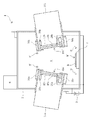
2 真空チャンバー
3 スパッタ電力供給用電源
4 基板ホルダー
5 排気装置
6 ガス供給装置
6’ スパッタガス導入供給口
6’’ 反応ガス供給口
10a,10b ターゲット
10a’,10b’ スパッタ面(対向面)
11a,11b ターゲットホルダー
12a,12b バッキングプレート
20a,20b ターゲット間磁場発生手段
30a,30b 補助磁場発生手段
K プラズマ発生空間
B 基体シート
B’ 被成膜面
AP 導電性金属薄膜
AN 窒化物半導体薄膜
Claims (7)
- 透明な基体シート上に、導電性金属薄膜と、当該導電性金属薄膜の上下に積層された窒化物半導体薄膜とを含む積層構造を設けてなる透明導電膜であって、前記導電性金属薄膜が、Pd、Nd及びNiから選択される1種又は2種以上を合計0.5〜10wt%ドーピングした銀からなる膜であり、前記窒化物半導体薄膜がCu、Sn及びTiから選択される1種又は2種以上を合計0.1〜10wt%含む窒化アルミニウムの薄膜であることを特徴とする透明導電膜。
- 前記導電性金属薄膜の厚みが5〜30nmであり、前記窒化物半導体薄膜の厚みが5〜70nmであることを特徴とする請求項1に記載の透明導電膜。
- 前記積層構造の厚みが15〜170nmであることを特徴とする請求項1又は2に記載の透明導電膜。
- 可視光透過率が85%〜99%、かつ、シート抵抗値が0.1〜10Ω/□であることを特徴とする、請求項1〜3のいずれか1項に記載の透明導電膜。
- Cu、Sn及び/Tiから選択される1種又は2種以上を0.1〜10wt%含むアルミニウムをターゲットとし、不活性ガスであるスパッタガス及び窒素ガスを含有する反応ガスを用いて、対向ターゲットスパッタ法によって窒化物半導体薄膜を成膜する工程と、Pd、Nd及びNiから選択される1種又は2種以上を合計0.5〜10wt%ドーピングした銀をターゲットとし、不活性ガスであるスパッタガスを用いて対向ターゲットスパッタ法によって導電性金属薄膜を成膜する工程と、を含む、請求項1〜4のいずれか1項に記載の透明導電膜の製造方法。
- 前記対向ターゲットスパッタ法に用いられる装置が、間隔をおいて互いに対向すると共に、一方の側方位置に配置される成膜対象となる基板側に開口するように互いに対向する面を傾斜させて一対のターゲットが配置され、前記一対のターゲットの各々を囲むようにその周縁に沿って配置される筒状の一対の永久磁石を備える補助磁場発生手段を有することを特徴とする対向ターゲットスパッタ装置である、請求項5に記載の透明導電膜の製造方法。
- 前記成膜工程が、基板を加熱することなく行われることを特徴とする、請求項5又は6に記載の透明導電膜の製造方法。
Priority Applications (3)
| Application Number | Priority Date | Filing Date | Title |
|---|---|---|---|
| JP2012169184A JP5938290B2 (ja) | 2012-07-31 | 2012-07-31 | 透明導電膜及びその製造方法 |
| PCT/JP2013/070618 WO2014021325A1 (ja) | 2012-07-31 | 2013-07-30 | 透明導電膜及びその製造方法 |
| TW102127409A TWI630658B (zh) | 2012-07-31 | 2013-07-31 | Transparent conductive film and method of manufacturing same |
Applications Claiming Priority (1)
| Application Number | Priority Date | Filing Date | Title |
|---|---|---|---|
| JP2012169184A JP5938290B2 (ja) | 2012-07-31 | 2012-07-31 | 透明導電膜及びその製造方法 |
Publications (3)
| Publication Number | Publication Date |
|---|---|
| JP2014028986A JP2014028986A (ja) | 2014-02-13 |
| JP2014028986A5 JP2014028986A5 (ja) | 2015-09-17 |
| JP5938290B2 true JP5938290B2 (ja) | 2016-06-22 |
Family
ID=50027998
Family Applications (1)
| Application Number | Title | Priority Date | Filing Date |
|---|---|---|---|
| JP2012169184A Expired - Fee Related JP5938290B2 (ja) | 2012-07-31 | 2012-07-31 | 透明導電膜及びその製造方法 |
Country Status (3)
| Country | Link |
|---|---|
| JP (1) | JP5938290B2 (ja) |
| TW (1) | TWI630658B (ja) |
| WO (1) | WO2014021325A1 (ja) |
Families Citing this family (6)
| Publication number | Priority date | Publication date | Assignee | Title |
|---|---|---|---|---|
| JP6366221B2 (ja) * | 2012-09-21 | 2018-08-01 | コニカミノルタ株式会社 | 透明電極、及び電子デバイス |
| KR102341963B1 (ko) | 2014-05-23 | 2021-12-22 | 더 리젠츠 오브 더 유니버시티 오브 미시건 | 광전자 및 광자 공학 응용을 위한 도핑된 귀금속 초박막 |
| CN104269221A (zh) * | 2014-08-29 | 2015-01-07 | 上海蓝沛新材料科技股份有限公司 | 一种利用含钯化合物的墨水制备透明导电膜的方法 |
| JP2016191967A (ja) * | 2015-03-30 | 2016-11-10 | 株式会社神戸製鋼所 | 窒素含有Cu合金膜、積層膜、およびこれらの製造方法、ならびにCu合金スパッタリングターゲット |
| CN113913775A (zh) * | 2021-09-30 | 2022-01-11 | 浙江师范大学 | 对向靶磁控溅射无损伤薄膜沉积系统 |
| CN114622162A (zh) * | 2022-03-14 | 2022-06-14 | 南京邮电大学 | 一种耐高温透明导电复合薄膜及其制备方法和应用 |
Family Cites Families (6)
| Publication number | Priority date | Publication date | Assignee | Title |
|---|---|---|---|---|
| JPS63205609A (ja) * | 1987-02-20 | 1988-08-25 | Unitika Ltd | 熱線反射膜 |
| JPH07105740A (ja) * | 1993-10-08 | 1995-04-21 | Mitsui Toatsu Chem Inc | 透明導電性フィルム |
| JP4510967B2 (ja) * | 1999-12-03 | 2010-07-28 | 大阪府 | 導電性光選択透過シート |
| JP2004047216A (ja) * | 2002-07-10 | 2004-02-12 | Central Glass Co Ltd | 透明導電膜 |
| JP4961786B2 (ja) * | 2006-03-17 | 2012-06-27 | 住友金属鉱山株式会社 | 透明導電膜、およびこれを用いた透明導電性フィルム |
| JP5059430B2 (ja) * | 2007-01-26 | 2012-10-24 | 株式会社大阪真空機器製作所 | スパッタ方法及びスパッタ装置 |
-
2012
- 2012-07-31 JP JP2012169184A patent/JP5938290B2/ja not_active Expired - Fee Related
-
2013
- 2013-07-30 WO PCT/JP2013/070618 patent/WO2014021325A1/ja active Application Filing
- 2013-07-31 TW TW102127409A patent/TWI630658B/zh not_active IP Right Cessation
Also Published As
| Publication number | Publication date |
|---|---|
| JP2014028986A (ja) | 2014-02-13 |
| WO2014021325A1 (ja) | 2014-02-06 |
| TW201411724A (zh) | 2014-03-16 |
| TWI630658B (zh) | 2018-07-21 |
Similar Documents
| Publication | Publication Date | Title |
|---|---|---|
| JP5938290B2 (ja) | 透明導電膜及びその製造方法 | |
| El Hajj et al. | Optimization of ZnO/Ag/ZnO multilayer electrodes obtained by Ion Beam Sputtering for optoelectronic devices | |
| JP2010241638A (ja) | 金属ナノ粒子層を挟んだ薄膜積層体 | |
| CN102159971A (zh) | 防反射膜的成膜方法、防反射膜和成膜装置 | |
| CN103258966B (zh) | 用于有机发光装置的反射阳极电极及其制造方法 | |
| TW200918479A (en) | Conductor layer manufacturing method | |
| JP5580972B2 (ja) | スパッタリング複合ターゲット | |
| CN103171187A (zh) | 一种三明治式透明导电薄膜及制备方法 | |
| WO2013099084A1 (ja) | 有機el素子の製造方法 | |
| CN103924191A (zh) | 在基片上镀制ito薄膜的方法 | |
| JP5447240B2 (ja) | マグネトロンスパッタリング装置および透明導電膜の製造方法 | |
| JP2014218042A (ja) | 透明断熱シート及びその製造方法 | |
| Lim et al. | Transparent Ti-In-Sn-O multicomponent anodes for highly efficient phosphorescent organic light emitting diodes | |
| JP2017193755A (ja) | 透明導電膜の製造方法、及び透明導電膜 | |
| CN105517335A (zh) | 一种触控屏线路板 | |
| CN104681208A (zh) | 一种提高纳米银薄膜导电性的方法 | |
| JPWO2009028372A1 (ja) | 透明導電膜の形成方法 | |
| CN103203912B (zh) | 一种新型azo镀膜玻璃及其制备工艺 | |
| JP6484098B2 (ja) | 透明導電フィルムおよび表示デバイス、並びに、透明導電フィルムの製造方法および表示デバイスの製造方法 | |
| Sung et al. | Transparent conductive titanium-doped indium oxide films prepared by a magnetic null discharge sputter source | |
| JPH0273963A (ja) | 低温基体への薄膜形成方法 | |
| JP2013202893A (ja) | 透明断熱シート | |
| JP5881995B2 (ja) | 透明導電膜及びその製造方法 | |
| KR20120000317A (ko) | 전자 물질막 형성 장치 | |
| JP2004247060A (ja) | 透明導電性酸化物複合体とこれを用いた太陽電池および表示装置 |
Legal Events
| Date | Code | Title | Description |
|---|---|---|---|
| A521 | Written amendment |
Free format text: JAPANESE INTERMEDIATE CODE: A523 Effective date: 20150730 |
|
| A621 | Written request for application examination |
Free format text: JAPANESE INTERMEDIATE CODE: A621 Effective date: 20150730 |
|
| A521 | Written amendment |
Free format text: JAPANESE INTERMEDIATE CODE: A821 Effective date: 20150730 |
|
| A131 | Notification of reasons for refusal |
Free format text: JAPANESE INTERMEDIATE CODE: A131 Effective date: 20160127 |
|
| A521 | Written amendment |
Free format text: JAPANESE INTERMEDIATE CODE: A523 Effective date: 20160325 |
|
| TRDD | Decision of grant or rejection written | ||
| A01 | Written decision to grant a patent or to grant a registration (utility model) |
Free format text: JAPANESE INTERMEDIATE CODE: A01 Effective date: 20160427 |
|
| A61 | First payment of annual fees (during grant procedure) |
Free format text: JAPANESE INTERMEDIATE CODE: A61 Effective date: 20160516 |
|
| R150 | Certificate of patent or registration of utility model |
Ref document number: 5938290 Country of ref document: JP Free format text: JAPANESE INTERMEDIATE CODE: R150 |
|
| LAPS | Cancellation because of no payment of annual fees |