WO2013154191A1 - X線露出制御装置、x線画像検出装置及びx線画像撮影システム - Google Patents
X線露出制御装置、x線画像検出装置及びx線画像撮影システム Download PDFInfo
- Publication number
- WO2013154191A1 WO2013154191A1 PCT/JP2013/061115 JP2013061115W WO2013154191A1 WO 2013154191 A1 WO2013154191 A1 WO 2013154191A1 JP 2013061115 W JP2013061115 W JP 2013061115W WO 2013154191 A1 WO2013154191 A1 WO 2013154191A1
- Authority
- WO
- WIPO (PCT)
- Prior art keywords
- ray
- pixel
- dose
- irradiation
- exposure control
- Prior art date
Links
Images


Classifications
-
- H—ELECTRICITY
- H05—ELECTRIC TECHNIQUES NOT OTHERWISE PROVIDED FOR
- H05G—X-RAY TECHNIQUE
- H05G1/00—X-ray apparatus involving X-ray tubes; Circuits therefor
- H05G1/08—Electrical details
- H05G1/26—Measuring, controlling or protecting
- H05G1/30—Controlling
-
- A—HUMAN NECESSITIES
- A61—MEDICAL OR VETERINARY SCIENCE; HYGIENE
- A61B—DIAGNOSIS; SURGERY; IDENTIFICATION
- A61B6/00—Apparatus for radiation diagnosis, e.g. combined with radiation therapy equipment
- A61B6/42—Apparatus for radiation diagnosis, e.g. combined with radiation therapy equipment with arrangements for detecting radiation specially adapted for radiation diagnosis
- A61B6/4208—Apparatus for radiation diagnosis, e.g. combined with radiation therapy equipment with arrangements for detecting radiation specially adapted for radiation diagnosis characterised by using a particular type of detector
- A61B6/4233—Apparatus for radiation diagnosis, e.g. combined with radiation therapy equipment with arrangements for detecting radiation specially adapted for radiation diagnosis characterised by using a particular type of detector using matrix detectors
-
- A—HUMAN NECESSITIES
- A61—MEDICAL OR VETERINARY SCIENCE; HYGIENE
- A61B—DIAGNOSIS; SURGERY; IDENTIFICATION
- A61B6/00—Apparatus for radiation diagnosis, e.g. combined with radiation therapy equipment
- A61B6/54—Control of apparatus or devices for radiation diagnosis
- A61B6/542—Control of apparatus or devices for radiation diagnosis involving control of exposure
-
- H—ELECTRICITY
- H04—ELECTRIC COMMUNICATION TECHNIQUE
- H04N—PICTORIAL COMMUNICATION, e.g. TELEVISION
- H04N23/00—Cameras or camera modules comprising electronic image sensors; Control thereof
- H04N23/70—Circuitry for compensating brightness variation in the scene
- H04N23/73—Circuitry for compensating brightness variation in the scene by influencing the exposure time
-
- H—ELECTRICITY
- H04—ELECTRIC COMMUNICATION TECHNIQUE
- H04N—PICTORIAL COMMUNICATION, e.g. TELEVISION
- H04N25/00—Circuitry of solid-state image sensors [SSIS]; Control thereof
- H04N25/60—Noise processing, e.g. detecting, correcting, reducing or removing noise
- H04N25/63—Noise processing, e.g. detecting, correcting, reducing or removing noise applied to dark current
-
- H—ELECTRICITY
- H04—ELECTRIC COMMUNICATION TECHNIQUE
- H04N—PICTORIAL COMMUNICATION, e.g. TELEVISION
- H04N5/00—Details of television systems
- H04N5/30—Transforming light or analogous information into electric information
- H04N5/32—Transforming X-rays
Definitions
- the present invention relates to an X-ray exposure control apparatus having an X-ray exposure control function, an X-ray image detection apparatus including the X-ray exposure control apparatus, and an X-ray image capturing system including the X-ray image detection apparatus.
- an X-ray film method in which an X-ray image is directly recorded on an X-ray film and developed using a screen film photographing system combining a fluorescent screen and an X-ray film, or an X-ray image Is recorded as a latent image on a stimulable phosphor sheet or the like called an imaging plate (IP), and then scanned with a laser to read X-ray emission and acquire X-ray image data as digital data.
- Method and X-ray images can be read directly and directly with an X-ray detector such as a flat panel detector (FPD: Flat Panel Detector) with an X-ray sensitive layer placed on a TFT (thin film transistor) substrate.
- a digital radiography (DR: Digital Radiography) method for acquiring X-ray image data as digital data is generally used.
- any of the above-described X-ray imaging systems X-rays emitted from an X-ray source are detected, and when an appropriate X-ray dose is reached, automatic exposure control for stopping X-ray irradiation ( AEC) mechanism is provided. Since the X-ray imaging system includes an AEC mechanism, an X-ray image having an appropriate density can always be acquired in the same imaging environment even when imaging various different parts. .
- AEC X-ray imaging system
- Such a conventional AEC is called a phototimer using an ion chamber having a so-called ionization chamber or photoelectric conversion element.
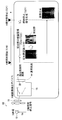
- an X-ray imaging system 200 is provided to face an X-ray source 202 and the X-ray source 202 and receives an X-ray image transmitted through a subject 204 (imaging site).
- Dose detection provided with an image detection dedicated device (hereinafter referred to as X-ray detection device) 206, and an X-ray detection device 206, which is disposed between the imaging position of the subject 204 and the X-ray detection device 206, and at a plurality of positions serving as a daylighting field.
- X-ray detection device image detection dedicated device
- an AEC unit 212 for controlling the stop of the X-ray source 202 according to the integrated amount (exposure amount) of X-rays detected by the X-ray sensor 208 in the daylighting field of the dose detector 210.
- the dose detector 210 and the AEC unit 212 constitute an AEC mechanism.
- a plurality of, in the illustrated example, three X-ray sensors 208 (labeled RGB) are attached to the dose detector 210, but are fixed to the X-ray detection device 206. For this reason, the lighting field is fixed.
- the daylight field is “blue (B)” and “green (G)” corresponding to the lung field in front of the chest, and “red (B)” in the abdomen.
- X-rays are irradiated from the X-ray source 202 toward the subject 204 (imaging site), and the X-rays irradiated to the lighting field of the subject 204 are X-rays of the dose detector 210.
- the X-ray dose detected by the X-ray sensor 208 is integrated by the AEC unit 212, detected by the X-ray sensor 208, and integrated by the AEC unit 212.
- the stop signal Sp for stopping the X-ray source 202 is generated by the AEC unit 212 and sent from the AEC unit 212 to the X-ray source 202, and the X-ray source 202 is stopped.
- the dose detector 210 and the X-ray detection are performed.
- the device 206 is also integrated (see Patent Documents 1 and 2).
- some pixels of the X-ray image detection device are used as pixels for detecting an X-ray dose.
- the present invention solves the above-mentioned problems of the prior art, and can recognize and determine the daylighting field of the subject to be photographed during photographing from the image during X-ray photographing, and is suitable for the subject, that is, the photographing part.
- X-ray irradiation can be stopped with an appropriate exposure dose (exposure), that is, the irradiation dose at the time of X-ray imaging can be appropriately controlled according to the subject.
- An object of the present invention is to provide an X-ray exposure control device, an X-ray image detection device, and an X-ray image photographing system that can always obtain an X-ray image having an appropriate density in the same photographing environment.
- an X-ray exposure control apparatus is an X-ray exposure control apparatus that controls the amount of X-rays irradiated from an X-ray source to an imaging target.
- the X-ray exposure control is used in an X-ray image detection apparatus that detects an X-ray image of an imaging target by irradiating the imaging target with X-rays from an X-ray source, and controls the accumulated dose of X-rays irradiated to the imaging target
- An X-ray detection element comprising a plurality of dose detection pixels for detecting a dose during X-ray irradiation, and a dose detection pixel to be used from among the plurality of dose detection pixels during X-ray irradiation
- the region setting unit sets a use pixel region by analyzing dose information of a plurality of dose detection pixels at a predetermined timing.
- the predetermined timing is preferably a preset fixed timing or an externally designated timing, and the designated timing is a preset value set in accordance with an imaging target, an X-ray source tube current. And based on at least one of the tube voltages of the X-ray source.
- the region setting unit combines a plurality of pixel features and neighboring pixel features from the dose information of a plurality of dose detection pixels, and irradiation with a subject pixel representing an imaging target to be a subject or X-ray irradiation It is preferable to identify a field pixel and set a use pixel region including a subject pixel or an irradiation field pixel as a use dose detection pixel. Further, it is preferable that the region setting unit specifies a subject pixel or an irradiation field pixel and sets a part of the subject pixel or a part of the irradiation field pixel as a use dose detection pixel.
- the area setting unit sets a use pixel area by combining a plurality of pixel characteristics and neighboring pixel characteristics from dose information of a plurality of dose detection pixels. Moreover, it is preferable that the area setting unit sets a use pixel area using pixel characteristics from dose information of a plurality of dose detection pixels. Moreover, it is preferable that the area setting unit specifies the use dose detection pixel based on the pixel feature of the reduced image in which the plurality of dose detection pixels are combined into one pixel.
- the area setting unit includes a plurality of modes that can be selected according to a preset imaging target, and sets the use dose detection pixel according to the mode selected according to the imaging target.
- the region setting unit preferably includes a plurality of modes, and sets the use dose detection pixels in a mode selected according to the feature of the image.
- the area setting unit preferably determines a mode to be selected based on the characteristics of the subject area or the irradiation field area.
- the region setting unit preferably includes a plurality of modes, and each of the plurality of modes detects a use dose detection pixel, and determines a use dose detection pixel to be set according to the feature of the image.
- the multiple modes are used for detecting the dose on the high-dose side pixel in the cumulative histogram of the dose set for the specified subject pixel, pixel in the irradiation field, or multiple pixel features and neighboring pixel features.
- at least one mode is included.
- the first mode may be a mode for imaging the lung field
- the second mode may be a mode for imaging the bone.
- the plurality of modes preferably include a mode for designating a pixel area to be used from the outside, or a mode for photographing with a preset dose.
- the plurality of modes includes a first mode in which a use dose detection pixel is set based on the dose of the specified subject pixel, and a use dose detection pixel that is set based on the dose of the specified irradiation field pixel.
- a third mode in which a pixel area to be used is set by combining a plurality of pixel features and neighboring pixel characteristics
- a fourth mode in which the pixel area to be used is set by using a pixel feature. preferable.
- the X-ray detection element starts detecting, holding, and accumulating doses by a plurality of dose detection pixels at a start timing when the X-ray source starts X-ray irradiation on the imaging target.
- the X-ray detection element preferably detects the start timing by a plurality of dose detection pixels.
- the X-ray exposure control apparatus according to the first aspect further includes an acquisition unit that acquires a start signal indicating a start timing for starting X-ray irradiation from the X-ray source to the imaging target.
- the detection element preferably starts dose detection by a plurality of dose detection pixels according to the start signal acquired by the acquisition unit.
- an acquisition unit acquires a start signal from the outside.
- the signal generation unit generates a stop signal for stopping the X-ray irradiation when the detected dose of the dose detection pixel in the use pixel region reaches or exceeds a preset threshold value. It is preferable. Moreover, it is preferable that the threshold is set based on an imaging target, imaging conditions, or a plurality of modes. The threshold value is preferably corrected so as to absorb the characteristic difference of the X-ray detection element, or preferably corrected so as to absorb the delay difference caused by the transmission unit.
- the X-ray exposure control apparatus further stops the X-ray irradiation by the X-ray source based on information different from the detection dose of the dose detection pixels in the use pixel region. It is preferable to have a second signal generation unit that generates the stop signal. Further, the information different from the detected dose is preferably information on an imaging target, information on imaging conditions, or information on a plurality of modes. Further, at least a notification for informing a signal type of a stop signal based on the detected dose of the dose detection pixel in the use pixel region and a second stop signal based on information different from the detected dose of the dose detection pixel. It is preferable to have a unit.
- the area setting unit reads out dose information of a plurality of dose detection pixels analyzed at a predetermined timing from the X-ray detection element.
- the signal generation unit sets the use pixel region included as the use dose detection pixel by the region setting unit, and then sets the dose of the use dose detection pixel in the use pixel region for each predetermined monitoring timing. It is preferable that the stop signal is generated when the accumulated dose reaches or exceeds the threshold value.
- the X-ray exposure control apparatus further reads out the dose detected by the plurality of dose detection pixels of the X-ray detection element at every predetermined sampling timing during the X-ray irradiation, and receives the dose information.
- the area setting unit reads out dose information of a plurality of dose detection pixels to be analyzed at a predetermined timing from the storage unit.
- a storage unit accumulate
- the signal generation unit reads the dose of the use dose detection pixel in the use pixel region from the storage unit at every predetermined monitoring timing after setting the use pixel region included in the region setting unit as the use dose detection pixel. It is preferable that the stop signal is generated when the accumulated dose reaches or exceeds the threshold value as compared with a threshold value set in advance according to the imaging conditions.
- the X-ray exposure control apparatus further reads and accumulates doses detected by a plurality of dose detection pixels of the X-ray detection element at predetermined sampling timings during X-ray irradiation.
- a storage unit that performs storage processing for each dose detection pixel; a storage unit that is referred to for storage processing by the storage unit and stores a stored dose for each dose detection pixel; and a region setting unit
- the second storage area that stores the analysis dose for each dose detection pixel that is referred to by the analysis process and used for the analysis process for setting the use pixel area, and the dose in the first storage area at a predetermined timing It is preferable that the accumulated dose for each detection pixel is read out and stored in the second storage area as the analysis dose for each dose detection pixel.
- the accumulation unit accumulates the detected dose for each dose detection pixel of the X-ray detection element to the accumulated dose for each dose detection pixel read from the first storage area of the storage unit at each sampling timing.
- the accumulated dose for each dose detection pixel stored in the storage area is updated, and the area setting unit reads and reads out the analysis dose for each dose detection pixel stored in the second storage area of the storage unit at a predetermined timing. It is preferable to perform analysis processing based on the analysis dose for each dose detection pixel, determine a dose detection pixel to be used for generating a stop signal, and set a use pixel region including the dose detection pixel. Further, it is preferable that the accumulation process by the accumulation unit and the analysis process by the area setting unit are controlled to be performed in parallel.
- the X-ray image detection apparatus is irradiated with the X-ray exposure control apparatus according to the first aspect and the start of X-ray irradiation of the X-ray source. It has an X-ray image detection unit for detecting X-rays transmitted through the imaging target and detecting an X-ray image of the imaging target before the stop.
- the X-ray image detection unit includes a plurality of X-ray image detection pixels that detect X-rays that have passed through the imaging target between the start and end of irradiation of the X-rays of the X-ray source. An element is preferred.
- the X-ray image detection element is integrated with the X-ray detection element, and the plurality of dose detection pixels have a configuration different from that of the plurality of X-ray image detection pixels. It is preferable that the X-ray image detection element is a non-destructive readable element and a part of the plurality of X-ray image detection pixels is also used as a plurality of dose detection pixels. .
- an X-ray imaging system includes an X-ray source that irradiates X-rays and the X-ray image detection apparatus according to the second aspect.
- the X-ray source receives an X-ray irradiation start signal from an external device or an X-ray image detection device, starts X-ray irradiation, and receives an X-ray irradiation stop signal from the X-ray image detection device. The X-ray irradiation is stopped upon reception.
- stable X-ray exposure control can be performed regardless of the positioning of the subject by recognizing and determining the daylighting field of the subject during X-ray imaging. . Therefore, according to the present invention, X-ray irradiation can be stopped at an appropriate exposure dose (exposure) according to the subject (imaging site), that is, the irradiation dose at the time of X-ray imaging is appropriate according to the subject. X-ray images with an appropriate density can always be acquired in the same imaging environment even when imaging various different parts. That is, according to the present invention, it is possible to perform stable imaging at an appropriate dose regardless of where the subject, that is, the imaging region, or anywhere in the whole body.
- FIG. 1 is a schematic explanatory view schematically showing an example of an X-ray imaging system to which an X-ray image detection apparatus including an X-ray exposure control apparatus according to a first embodiment of the present invention is applied. It is explanatory drawing explaining one Example of the control apparatus of the X-ray image detection apparatus shown in FIG. It is explanatory drawing explaining one Example of the X-ray image detection device used for the X-ray imaging system shown in FIG. It is a block diagram of one Example of the AEC part used for the control apparatus of the X-ray image detection apparatus shown in FIG. 5 is a flowchart for explaining an example of an AEC procedure performed by an AEC unit shown in FIG. 4.
- FIG. 1 is a schematic explanatory view schematically showing an example of an X-ray imaging system to which an X-ray image detection apparatus including an X-ray exposure control apparatus according to a first embodiment of the present invention is applied. It is explanatory drawing explaining one Example of the control apparatus of the X-ray image detection apparatus shown in
- FIG. 5 is an explanatory diagram schematically illustrating an example of an AEC procedure performed by an AEC unit illustrated in FIG. 4. It is a chart which shows typically an example of the flow of X-ray imaging of the X-ray imaging system shown in FIG.
- FIG. 5 is a schematic explanatory diagram for explaining an example of a read-out operation performed in a read accumulation unit of the AEC unit shown in FIG. 4.
- (A) is a schematic explanatory drawing explaining an example of the pixel configuration of the X-ray image detection device shown in FIG. 3, and
- (B) and (C) explain an example of the pixel configuration of the exposure control pixel, respectively. It is typical explanatory drawing to do.
- FIG. 18 is a block diagram of another example of the AEC unit of the X-ray image detection device shown in FIG. 17. It is a flowchart explaining an example of the procedure of AEC performed in the AEC part shown in FIG.
- FIG. 1 It is explanatory drawing which illustrates typically an example of the procedure of AEC performed in the AEC part shown in FIG.
- (A) is a schematic diagram showing a conventional X-ray imaging system
- (B) and (C) are schematic diagrams showing a dose detector and an X-ray image used in the conventional X-ray imaging system, respectively.
- FIG. 1 is a schematic diagram showing a schematic configuration of an example of an X-ray imaging system using an X-ray image detection apparatus including an X-ray exposure control apparatus according to the first embodiment of the present invention.
- the X-ray imaging system 10 of the first embodiment of the present invention includes an X-ray source 12 and an X-ray image detection device 14, and the X-ray image detection device 14 is an X-ray image.
- An X-ray image detection device (hereinafter simply referred to as an image detection device) 18 provided at a position facing the source 12 and receiving an X-ray image transmitted through the subject 16 (imaging site), and the X-ray source 12 and image detection
- a control device 20 that controls the overall operation of the X-ray imaging system 10 such as operation control of the device 18 and image processing of the X-ray image.
- the X-ray imaging system 10 is an imaging table such as a standing imaging table for imaging the subject 16 in a standing position, a lying imaging table for imaging in a lying position, and an X-ray source 12.
- a radiation source moving device or the like is provided for setting the device in a desired direction and position.
- the exposure control pixel 76 excluding the portion of the normal pixel 44 for image detection of the image detection device 18 in the X-ray image detection apparatus 14.
- each part of the control apparatus 20 except the part which processes the X-ray image by the normal pixel 44 comprises the X-ray exposure control apparatus which concerns on 1st Embodiment of this invention.
- the X-ray source 12 includes an X-ray tube that emits X-rays and an irradiation field limiter (collimator) that limits an irradiation field of the X-rays emitted by the X-ray tube.
- the X-ray tube has a cathode made of a filament that emits thermoelectrons, and an anode (target) that emits X-rays when the thermoelectrons emitted from the cathode collide.
- the irradiation field limiter has, for example, a plurality of lead plates that shield X-rays arranged in a cross pattern, and an irradiation opening that transmits X-rays is formed in the center, and the position of the lead plate is moved. The irradiation field is limited by changing the size of the irradiation opening.
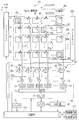
- the control device 20 includes an X-ray detection control unit (hereinafter simply referred to as a detection control unit) 22 that comprehensively controls the operation of the entire device, and high voltage generation connected to the detection control unit 22.
- Device 24 irradiation switch 26, input device 28, display 30, and memory 32.
- the detection control unit 22 includes a device control unit 34, a radiation source control unit 36, a memory 38, and an X-ray exposure control unit (hereinafter also referred to as an AEC unit) 40.
- the high voltage generator 24 boosts the input voltage with a transformer to generate a high voltage tube voltage and supplies it to the X-ray source 12 through a high voltage cable.
- the radiation source control unit 36 is a tube voltage that determines the energy spectrum of the X-rays that the X-ray source 12 irradiates, a tube current that determines the amount of irradiation per unit time, the irradiation start of the X-ray source 12, the irradiation stop or end, and the X Control the irradiation time of the line.
- the irradiation switch 26 is, for example, a two-stage push switch operated by an operator such as a radiographer, and generates a warm-up start signal for starting the warm-up of the X-ray source 12 by one-stage push. Then, an irradiation start signal for starting irradiation of the X-ray source 12 is generated. These signals are input to the radiation source controller 36 through a signal cable.
- the radiation source control unit 36 starts power supply from the high voltage generator 24 to the X-ray source 12 when receiving the irradiation start signal from the irradiation switch 26, and receives the irradiation stop signal from the AEC unit 40.
- the power supply from the high voltage generator 24 to the X-ray source 12 is stopped, and the X-ray irradiation by the X-ray source 12 is stopped.
- the memory 32 stores several types of imaging conditions such as tube voltage and tube current in advance.
- the photographing conditions are manually set by the operator through the input device 28.
- the radiation source control unit 36 tries to irradiate X-rays with the tube voltage and tube current irradiation time product of the set imaging conditions.
- X-ray irradiation is performed even if it is less than the tube current irradiation time product (irradiation time) to be irradiated by the radiation source control unit 36. Function to stop.
- the imaging conditions of the X-ray source 12 include the tube current irradiation time product (irradiation).
- the maximum value is also set.
- the set tube current irradiation time product is preferably a value corresponding to the imaging region.
- the device control unit 34 controls the operation of the image detection device 18 in accordance with an input operation from the operator via the input device 28. Specifically, the device control unit 34 performs various controls such as power on / off of the image detection device 18 and mode switching to a standby mode or a shooting mode. In addition, the device controller 34 preferably has a function of performing various image processing such as offset correction, sensitivity correction, and defect correction on the X-ray image data in the memory 38. These various image processes will be described later. After the X-ray image data from the image detection device 18 is stored in the memory 38, the above-described various image processing is performed by the device control unit 34 of the control device 20, but the image processed X-ray image is displayed on the display. In addition to being displayed on the screen 30, the data is stored again in a data storage such as the memory 38, a storage device (not shown), or an image storage server connected to the control device 20 via a network.
- a data storage such as the memory 38, a storage device (not shown), or an image storage server connected
- the control device 20 has a so-called console function, receives an input of an examination order including information such as a patient's sex, age, imaging region, and imaging purpose, and displays the examination order on the display 30.
- the examination order is input from an external system that manages patient information such as HIS (Hospital Information System) and RIS (Radiation Information System) and examination information related to radiation examination, or is manually input by an operator.
- the examination order includes radiographs such as the head, chest, and abdomen, front, side, oblique, PA (X-rays are irradiated from the back of the subject), and AP (X-rays are irradiated from the front of the subject). Directions are included.
- the operator confirms the contents of the inspection order on the display 30 and inputs photographing conditions corresponding to the contents through the operation screen displayed on the display 30.
- the image detection device 18 is an X-ray detection element of the present invention, and includes a DR-type flat panel detector (hereinafter referred to as FPD) 42 (see FIG. 3) and a housing that houses the FPD 42.
- the housing of the image detection device 18 has a substantially rectangular shape and a flat shape, and is for fixing the FPD 42 to a photographing stand (not shown).
- the image detection device 18 may be a detachable and portable cassette type electronic cassette.
- the casing that accommodates the FPD 42 is preferably a portable casing, and its planar size is the same size as a film cassette or an IP cassette (also called a CR cassette) (international standard ISO 4090).
- the FPD 42 includes a TFT active matrix substrate, and includes an imaging surface 46 in which a plurality of pixels 44 that accumulate charges according to the X-ray arrival dose are arranged on the substrate.
- the plurality of pixels 44 are two-dimensionally arranged in a matrix of n rows (x direction) ⁇ m columns (y direction) at a predetermined pitch.
- the FPD 42 has a scintillator (phosphor) that converts X-rays into visible light, and is an indirect conversion type in which visible light converted by the scintillator is photoelectrically converted by the pixels 44.
- the scintillator is made of CsI: Tl (thallium activated cesium iodide), GOS (Gd 2 O 2 S: Tb, gadolinium oxysulfide) or the like, and is arranged so as to face the entire imaging surface 46 in which the pixels 44 are arranged. Has been.
- the scintillator and the TFT active matrix substrate may be a PSS (Penetration Side Sampling) system in which the scintillator and the substrate are arranged in this order when viewed from the X-ray incident side.
- Side Sampling method may be used.
- a direct conversion type FPD using a conversion layer such as amorphous selenium
- a CMOS method may be used instead of the TFT method.
- the pixel 44 includes a photodiode 48 that is a photoelectric conversion element that generates charges (electron-hole pairs) upon incidence of visible light, a capacitor (not shown) that accumulates charges generated by the photodiode 48, and a switching element.
- a thin film transistor (TFT) 50 is provided. It is also possible to store charges in the photodiode 48 without providing a capacitor separately.
- the photodiode 48 has a structure in which a semiconductor layer (for example, PIN type) that generates electric charges and an upper electrode and a lower electrode are arranged above and below the semiconductor layer.
- the TFT 50 is connected to the lower electrode
- the bias line 52 is connected to the upper electrode.
- the bias lines 52 are provided as many as the number of rows (n rows) of the pixels 44 in the imaging surface 46, and are bound to one connection.
- the connection 53 is connected to a bias power supply 54. A bias voltage is applied from the bias power source 54 to the upper electrode of the photodiode 48 through the connection line 53 and the bias line 52.
- An electric field is generated in the semiconductor layer by applying a bias voltage, and charges (electron-hole pairs) generated in the semiconductor layer by photoelectric conversion move to the upper and lower electrodes, one of which is positive and the other is negative. As a result, charge is accumulated in the capacitor.
- the TFT 50 has a gate electrode connected to the scanning line 56, a source electrode connected to the signal line 58, and a drain electrode connected to the photodiode 48.
- the scanning lines 56 and the signal lines 58 are wired in a grid pattern.
- the scanning lines 56 are the number of rows of the pixels 44 in the imaging surface 46 (n rows), and the signal lines 58 are the number of columns of the pixels 44 (m columns). Min) each is provided.
- the scanning line 56 is connected to the gate driver 60, and the signal line 58 is connected to the signal processing circuit 62.
- the gate driver 60 drives the TFT 50 to accumulate a signal charge corresponding to the X-ray arrival dose in the pixel 44, a read (main reading) operation for reading the signal charge from the pixel 44, and a reset (empty reading). ) Make an action.
- the control unit 64 controls the start timing of each of the operations executed by the gate driver 60. In the accumulation operation, the TFT 50 is turned off, and signal charges are accumulated in the pixel 44 during that time.
- gate pulses G1 to Gn for simultaneously driving TFTs 50 in the same row are generated sequentially from the gate driver 60, the scanning lines 56 are sequentially activated one row at a time, and the TFTs 50 connected to the scanning lines 56 one row at a time. Turn on. The charge accumulated in the capacitor of the pixel 44 is read out to the signal line 58 and input to the signal processing circuit 62 when the TFT 50 is turned on.
- the signal processing circuit 62 includes an integrating amplifier 66, a CDS circuit (CDS) 68, a multiplexer (MUX) 70, an A / D converter (A / D) 72, and the like.
- the integrating amplifier 66 is individually connected to each signal line 58.
- the integrating amplifier 66 includes an operational amplifier 66a and a capacitor 66b connected between the input and output terminals of the operational amplifier 66a, and the signal line 58 is connected to one input terminal of the operational amplifier 66a.
- the other input terminal of the operational amplifier 66a is connected to the ground (GND).
- a reset switch 66c is connected in parallel to the capacitor 66b.
- the integrating amplifier 66 integrates the charges inputted from the signal line 58, converts them into analog voltage signals V1 to Vm, and outputs them.
- the MUX 70 is connected to the output terminal of the operational amplifier 66a in each column via the amplifier 74 and the CDS 68.
- An A / D 72 is connected to the output side of the MUX 70.
- the CDS 68 has a sample hold circuit, performs correlated double sampling on the output voltage signal of the integration amplifier 66 to remove noise, and holds the output voltage signal of the integration amplifier 66 for a predetermined period (sample hold).
- the MUX 70 selects one CDS 68 by an electronic switch in order from the CDS 68 of each column connected in parallel based on an operation control signal from a shift register (not shown), and outputs voltage signals V 1 to V output from the selected CDS 68. Vm is input to the A / D 72 serially.
- the A / D 72 converts the input voltage signals V1 to Vm into digital voltage signals, and transmits them as image data representing an X-ray image to the control device 20 (the memory 38 and / or the AEC unit 40 of the detection control unit 22). Output.
- An amplifier may be connected between the MUX 70 and the A / D 72.
- the control unit 64 When the voltage signals V1 to Vm for one row are read from the integrating amplifier 66 by the MUX 70, the control unit 64 outputs a reset pulse RST to the integrating amplifier 66 and turns on the reset switch 66c. As a result, the signal charge for one row stored in the capacitor 66b is discharged and reset. After resetting the integrating amplifier 66, the reset switch 66c is turned off again, and one of the sample and hold circuits of the CDS 68 is held after a lapse of a predetermined time, and the kTC noise component of the integrating amplifier 66 is sampled. Thereafter, a gate pulse of the next row is output from the gate driver 60 to start reading signal charges of the pixels 44 of the next row.
- the signal charge of the pixel 44 in the next row is held by another sample and hold circuit of the CDS 68 after a predetermined time has elapsed. These operations are sequentially repeated to read out the signal charges of the pixels 44 in all rows. In addition, high-speed driving is possible by performing pipeline processing that performs these processes simultaneously.
- one line of X-ray image data is output to the control device 20 and recorded in the memory 38.
- one screen of X-ray image is completed.
- the image data is recorded in the memory 38.
- an X-ray image of the subject is detected.
- a memory connected to the A / D 72 in the image detection device 18 is built in, and the digital image data output from the A / D 72 is temporarily stored in the built-in memory. After the image data representing the minute X-ray image is stored, the image data for one screen is immediately read from the built-in memory, output from the image detection device 18 to the control device 20, and recorded in the memory 38. good.
- the reset operation is an operation for sweeping out dark charges generated in the pixels 44 through the signal line 58.
- the reset operation is performed by, for example, a sequential reset method in which the pixels 44 are reset row by row.
- the sequential reset method similarly to the signal charge reading operation, gate pulses G1 to Gn are sequentially generated from the gate driver 60 to the scanning line 56, and the TFTs 50 of the pixels 44 are turned on line by line. While the TFT 50 is in the on state, dark charge flows from the pixel 44 to the capacitor 66 b of the integrating amplifier 66 through the signal line 58.
- the reset operation unlike the read operation, the charge accumulated in the capacitor 66b is not read by the MUX 70, and the reset pulse RST is output from the control unit 64 in synchronization with the generation of the gate pulses G1 to Gn.
- 66c is turned on, the electric charge accumulated in the capacitor 66b is discharged, and the integrating amplifier 66 is reset.
- the sequential reset method instead of the sequential reset method, multiple rows of array pixels are grouped as a group, and the reset is performed sequentially within the group, and the dark charge of the number of groups is simultaneously swept away.
- An all-pixel reset method that simultaneously sweeps out the dark charges may be used.
- the reset operation can be speeded up by a parallel reset method or an all-pixel reset method.
- a plurality of exposure control pixels 76 that are pixels for use are provided in the same imaging surface 46.
- the control pixel 76 is a pixel that is used to detect the arrival dose of X-rays that pass through the subject 16 and enter the imaging surface 36, and an irradiation stop signal in the AEC unit 40 of the detection control unit 22 of the control device 20. Functions as an AEC sensor for generating.
- the control pixel 76 occupies about several percent of the pixel 44 in the imaging surface 36.
- the control pixels 76 are preferably provided, for example, along a trajectory of a waveform that is symmetrical with respect to the center of the imaging surface 46 so as to be evenly distributed in the imaging surface 46 without being locally biased in the imaging surface 46. .
- the control pixels 76 are provided one by one in the column of pixels 44 to which the same signal line 58 is connected.
- the column in which the control pixel 76 is provided sandwiches a column in which no control pixel 76 is provided, for example, by 2 to 3 columns. Preferably it is provided.
- the position of the control pixel 76 is known when the FPD 42 is manufactured, and the FPD 42 preferably stores the positions (coordinates) of all the control pixels 76 in advance in, for example, a nonvolatile memory (not shown).
- control pixels 76 may be arranged locally and the arrangement of the control pixels 76 can be changed as appropriate.
- the exposure control pixels 76 are arranged at every other vertical and horizontal positions instead of the normal pixels at the positions of the normal pixels for image detection of the FPD 42, but the present invention is not limited to this. It may be arranged in a gap between normal pixels. In this case, since it is not necessary to use the position of the normal pixel as the control pixel 76, the pixel density can be increased accordingly.
- the TFT 50 Since the TFT 50 is not provided between the control pixel 76 and the signal line 58 and is directly connected to the signal line 58, the signal charge generated in the control pixel 76 is immediately read out to the signal line 58. The same applies to the normal pixel 44 in the same column during the accumulation operation in which the TFT 50 is turned off and the signal charge is accumulated. For this reason, the charge generated in the control pixel 76 always flows into the integrating amplifier 60 on the signal line 58 to which the control pixel 76 is connected.
- the charge from the control pixel 76 accumulated in the integrating amplifier 60 is output to the A / D 72 as a voltage value via the MUX 61 at a predetermined sampling period, and the A / D 72 digitally converts the input voltage value. It converts into a voltage value and outputs it to the control apparatus 20 (AEC part 40 of the detection control part 22) as pixel dose data for exposure control.
- the image detection device 18 of this embodiment has the some control pixel 76, it comprises the X-ray detection element of this invention.
- the image detection device 18 is basically configured as described above.
- the offset correction circuit subtracts the offset correction image acquired from the FPD 42 without irradiating the X-ray in units of pixels from the X-ray image, thereby removing fixed pattern noise caused by individual differences in the signal processing circuit 62 and the imaging environment. .
- the sensitivity correction circuit is also called a gain correction circuit, and corrects variations in sensitivity of the photodiode 48 of each pixel 44, variations in output characteristics of the signal processing circuit 62, and the like.
- Sensitivity correction is performed based on sensitivity correction data generated based on an image obtained by subtracting the offset correction image from an image obtained by irradiating a predetermined dose of X-rays in the absence of the subject.
- Sensitivity correction data is shifted from the reference value so that the output of each pixel is uniformly the same by multiplying the X-ray image after offset correction when a predetermined dose of X-rays is irradiated in the absence of the subject.
- Has a coefficient for correcting each pixel. For example, when the output of the pixel A is the reference 1 but the output of the pixel B is 0.8, the coefficient of the pixel B is 1.25 (1 / 0.8 1.25).
- the defect correction circuit linearly interpolates the pixel value of the defective pixel with the pixel values of the surrounding normal pixels based on the defective pixel information attached at the time of shipment. Further, the pixel value of the control pixel 76 in the daylighting field used for the AEC dose detection is similarly interpolated.
- the offset correction image and sensitivity correction data are acquired, for example, at the time of shipment of the image detection device 18, or are acquired by a manufacturer's service person at the time of regular maintenance, or by an operator at the start time of the hospital, and are stored in the internal memory of the device control unit 34. Is recorded at the time of correction. Note that the various image processing circuits described above may be provided in the detection control unit 22 of the control device 20 separately from the device control unit 34 to perform various image processing.
- the AEC unit 40 of the detection control unit 22 of the control device 20 is a feature of the present invention, and is a digital voltage signal (dose detection signal) detected by the control pixel 76 of the image detection device 18. Based on the dose data, the daylighting field of the subject 14 is recognized and automatically determined, and the X-ray irradiation of the X-ray source 12 is stopped when the accumulation amount of the dose data by the control pixel 76 in the daylighting field reaches the threshold value. This is for generating the irradiation stop signal Sp.
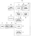
- the AEC unit 40 constitutes a main part of the X-ray exposure control apparatus of the present invention, and reads and accumulates exposure control pixel dose data (hereinafter simply referred to as dose data) from the image detection device 18, as shown in FIG.
- a lighting field recognition unit 86 that automatically recognizes the lighting field of the subject 16 based on the dose data
- an irradiation stop determination unit 88 that performs irradiation stop determination based on the accumulated dose data in the lighting field, and irradiation according to the irradiation stop determination
- An irradiation stop signal generation unit 90 that generates a stop signal Sp (first irradiation stop signal Sp1) and a second irradiation stop signal (Sp2) for stopping the X-ray irradiation of the X-ray source 12
- the second irradiation stop signal generation unit 92 to be generated and the (first and second) irradiation stop signal Sp (Sp1, Sp2) to stop the X-ray irradiation of the X-ray source 12 are sent to the radiation source control unit 36 and the high level.
- a transmission unit 94 that transmits to the X-ray source 12 via the voltage generator 24.
- the reading and accumulating unit 78 is detected by the control pixel 76 of the image detection device 18, acquired via the signal line 58 to which the control pixel 76 is connected, and A / D 72 at a predetermined sampling timing, for example, at a predetermined sampling cycle. Is obtained by adding the dose data read for each sampling from the start of X-ray irradiation to the predetermined sampling timing, for example, the sampling timing.
- the accumulated dose data stored in the accumulation storage area 80 is read out, and the accumulated dose data newly calculated and accumulated is calculated by adding the dose data read at the sampling timing to the read accumulated dose data. This is for storing in the storage area 80 for accumulation.
- the reading and accumulating unit 78 receives the irradiation start signal indicating the start timing of starting X-ray irradiation from the X-ray source 12 to the subject 14 to be imaged from the irradiation switch 26 until a predetermined timing. Is started, that is, measurement of time (sampling period) is started, but the irradiation start signal from the irradiation switch 26 is also transmitted to the image detection device 18, and the image detection device 18 is reset when the irradiation start signal is received. The operation shifts from the operation to the dose detection operation, and dose detection, holding and accumulation by the control pixel 76 is started.
- the start timing at which the X-ray source 12 starts X-ray irradiation is detected as a point in time when a dose is detected by the control pixel 76 of the image detection device 18, and this start timing signal is sent to the readout storage unit 78. You may make it transmit.
- the memory 84 stores the dose accumulated (accumulated) in the control pixel 76 of the image detection device 18 as accumulated dose data, and an accumulation storage area 80 for storing the accumulated dose data accumulated at each sampling timing. And an analysis storage area 82 for storing analysis dose data for daylight field recognition.
- the storage area 80 for accumulation in the memory 84 is a storage area for storing accumulated dose data accumulated in the control pixel 76 from the start of X-ray irradiation to the sampling timing for each control pixel 76.
- the accumulated dose data is updated to new accumulated dose data in which dose data sampled at the sampling period is accumulated at each sampling timing.
- the normal pixel 44 of the FPD 42 of the image detection device 18 is a TFT method including the TFT 50
- the normal pixel 44 and the control pixel 76 is reset, it is necessary to accumulate the accumulated dose data read at each sampling timing in a separate memory. Otherwise, total accumulated dose data cannot be obtained. Therefore, in the AEC unit 40 to which the image detection device 18 is connected, the accumulated dose data read from the control pixel 76 is sequentially accumulated at each sampling timing.
- a storage area 80 is required.
- the analysis storage area 82 is a storage area for storing analysis dose data for recognizing the daylighting field so that the daylighting field recognition unit 86 automatically determines the daylighting field, and accumulates at a predetermined timing. The accumulated dose data stored in the storage area 80 is read and stored.
- the analysis dose data captured in the analysis storage area 82 can be said to be image data by the control pixel 76, but since the number of pixels is small, the analysis dose data is a rough image. It is a sufficient image.
- the predetermined timing for reading the accumulated dose data as the analysis dose data from the accumulation storage area 80 is in a state where the SN ratio (S / N) has reached a certain level in order to make the lighting field recognition function stably. Is preferred. Further, such a predetermined timing is performed in advance for many cases of X-ray image capturing of the subject 14 using the image detection device 18, and the imaging region of the subject, the tube current and tube voltage of the X-ray source 12, etc. In accordance with at least one of the above, it is preferable to obtain the timing when the S / N level suitable for stably functioning the daylighting field is reached. In this case, the predetermined timing may be a preset fixed timing or a designated timing designated from the outside.
- such a designation timing may be a preset value set according to the imaging region, or a value set based on at least one of the tube current and the tube voltage of the X-ray source 12. Also good.
- timing can be shortened.
- the lighting field recognition unit 86 analyzes the image generated by the dose data of the plurality of control pixels 76 until the middle of the X-ray irradiation (each control pixel 76 has a value corresponding to the accumulated dose data), and stops irradiation.
- One or more use pixels (lighting fields) used for the irradiation stop determination of the determination unit 88 are determined, and an analysis process is performed based on the analysis dose data stored in the analysis storage area 82 of the memory 84 to obtain an X-ray.
- the lighting field of the imaging region 16a of the subject 16 to be imaged is automatically recognized and automatically determined.
- the daylight field recognition unit 86 performs analysis processing based on the read analysis dose data for each control pixel 76, and refers to the analysis storage area 82 of the memory 84 in order to determine the daylight field (use pixel). Then, the analysis dose data stored in the analysis storage area 82 may be read out at any time after the time when the analysis dose data is stored in the analysis storage area 82. Preferably, it is immediately after analysis dose data is stored in region 82.
- the daylight field recognition processing method performed by the daylight field recognition unit 86 is particularly limited if the daylight field can be recognized as a use pixel area including one or more use pixels or one or more use pixels, and the daylight field can be automatically determined. However, any recognition method may be used. For example, the following lighting field recognition method can be implemented. The following shows how to recognize a daylighting field.
- a control pixel 76 that satisfies a predetermined condition can be determined as a daylighting field based on statistics of dose data values of all control pixels 76.
- the dose data value of the control pixel 76 is simply referred to as a pixel value.
- the pixel described below means the control pixel 76. That is, the lighting field may be determined and set using pixel characteristics from the pixel values (dose information) of a plurality of control pixels (dose detection pixels) 76.
- control pixels 76 are determined as the daylighting fields.
- the variance ( ⁇ 2 ) of all pixel values is obtained, the control pixels 76 that are separated from the average value by ⁇ ⁇ ⁇ ( ⁇ is a constant) or more are excluded, and the remaining control pixels 76 are determined as the daylighting fields.
- the method of determining the daylighting field from only the distribution of all pixel values has a problem that it tends to fail if the area ratio of the subject region, the direct X-ray region, and the irradiation field region is extremely biased. It is preferably used when the area ratio of the region, direct X-ray region, and irradiation field region is provided.
- a binarized threshold value may be calculated by histogram analysis, and an area having a predetermined size including the center of gravity of pixels equal to or greater than the threshold value may be set as the daylighting field. Since the subject is directly surrounded by a high density region such as an X-ray region or the vicinity of the skin edge, and the high density centroid is likely to be in the subject, the region including the centroid can be set as the daylighting field.
- the predetermined size may be, for example, a circular region having a diameter of about 8 cm, which is employed in the conventional AEC, or may be determined based on the image size. For example, it may be a circular region whose diameter is half of the image side. Further, a high-concentration region that may be an X-ray region directly or a low-concentration region that may be outside the irradiation field may be excluded from the circular region.
- a subject region or subject including a part or all of the identified subject pixels is extracted by identifying and extracting a subject pixel by combining a plurality of features, for example, a plurality of pixel features and features of neighboring pixels. The entire area is determined as the lighting field.
- a subject region can be extracted by directly excluding an X-ray region based on a histogram and excluding an irradiation field region based on a difference histogram. .
- segmentation or machine learning can be used as disclosed in Japanese Patent Application Laid-Open No. 2004-079939.
- a subject it is only necessary to learn three subjects: a subject, direct X-rays, and an irradiation field as targets to be identified.
- machine learning may be performed on the likelihood of subject pixels, the likelihood of direct X-rays, and the likelihood of irradiation fields.
- AdaBoost Support Vector Machine, etc.
- the conditions and features for discriminating these three can be learned, and the subject area can be identified. it can.
- the subject area may be detected, and a pixel having a median value (30 to 70%, etc.) of pixel values in the subject area may be used as the daylighting field.
- the irradiation field area including the subject area and the direct X-ray area may be determined as the lighting field except for the irradiation field outside area. That is, for example, an irradiation field region or irradiation including a part or all of the specified irradiation field pixels is identified and extracted by combining a plurality of pixel features and features of neighboring pixels and identifying the irradiation field pixels irradiated with X-rays. The entire field area may be determined as the daylighting field. For example, by applying the irradiation field recognition method disclosed in Japanese Patent No.
- edge candidate points are detected along a radial linear direction set for a predetermined point in the image, and these A predetermined number of reference candidate lines can be obtained for the edge candidate points using Hough transform, and an area surrounded by these reference candidate lines can be determined as an irradiation field area.
- a plurality of irradiation field shape template information is stored and stored. Input the information that can specify the radiation field shape of the radiation image, and select the template corresponding to this based on the information of the radiation field shape input from the plurality of stored and saved field shape template information By matching the position and direction of the selected template and the radiographic image, it is possible to define an irradiation field of the radiographic image to be an irradiation field region.
- the irradiation field region may be detected, and a pixel having a median value (30 to 70%, etc.) of the pixel value of the irradiation field region may be used as the lighting field.
- a pixel having a median value (30 to 70%, etc.) of the pixel value of the irradiation field region may be used as the lighting field.
- an irradiation field region is detected, and a region in which a high-density pixel (such as 30% on the black side of the entire histogram width) that may be an X-ray region directly is excluded from pixels in the irradiation field region, or
- the median value (30 to 70%, etc.) of the area may be used as the daylighting field.
- the lighting field may be determined and set from the pixel values of the plurality of control pixels 76 by combining a plurality of pixel features and the features of neighboring pixels. For example, a differential centroid can be calculated based on the pixel values of adjacent pixels, and an area having a predetermined size including the differential centroid can be set as a lighting field. The predetermined size can be considered as in the case of the pixel centroid described above.
- the daylighting field may be specified based on the pixel characteristics of the reduced image in which the pixel values of the plurality of control pixels 76 are combined into one pixel.
- a specific control pixel 76 is further extracted from the subject area and determined as a lighting field. That is, after specifying the subject pixel, the daylight field is determined by statistical analysis of the specified subject pixel. For example, a pixel having a median value (40 to 60% in the cumulative histogram) in the subject area is determined as the daylighting field. By excluding the high-dose side and the low-dose side, it is possible to mitigate the influence when the X-ray region or the irradiation field region is mixed directly into the subject region. Conversely, a high dose (high exposure) control pixel may be used as a daylighting field, or a low dose (low exposure) control pixel may be used as a daylighting field.
- the lighting field recognizing unit 86 can prepare several modes that can be selected in accordance with an imaging target such as an imaging region and can use the mode by switching. For example, a pixel on the high dose side (for example, 80 to 90% in a cumulative histogram of dose) in a subject area, an irradiation field area, or an area set from a plurality of pixel features and neighboring pixel features is used as a lighting field ( High-exposure pixel priority designation) mode A, mode B, etc.
- the mode A for the examination for observing the lung field and to switch the mode B for the examination for observing the bone.
- a mode C is prepared in which pixels with intermediate doses (40 to 60% in the cumulative histogram) are used as lighting fields (standard designation) so that the three modes can be switched. Also good.
- the calculation method for the intermediate dose pixel is not limited to 40 to 60% in the above-described cumulative histogram, and a plurality of various calculation methods can be used.
- there is a method of taking 30 to 70% of the cumulative histogram as the median value and a high density area having a high possibility of a direct X-ray area is only a part of a predetermined ratio on the high density side with respect to the entire width of the histogram.
- a median value a low density region having a high possibility of a protector is excluded from only a predetermined ratio portion on the low density side with respect to the entire width of the histogram, and then a predetermined ratio of the cumulative histogram is taken. As a result, there is an advantage that the area of the protector is hardly affected.
- a plurality of selectable modes include at least a mode D for setting a daylighting field by analyzing pixel values (analysis dose data) of a plurality of control pixels 76 at a predetermined timing during X-ray irradiation, and an external mode. And a mode E for designating a daylighting field.
- a plurality of selectable modes include a mode F in which a lighting field (control pixel) is set based on the pixel value (dose data) of the subject pixel specified above, and a pixel of the irradiation field pixel specified above.
- At least one mode with I may be included.
- the lighting field recognition unit 86 may prepare a plurality of modes and set the lighting field (control pixel) in a mode selected according to the feature of the image.
- the plurality of modes prepared by the lighting field recognition unit 86 may be the various modes described above. For example, when looking at a histogram shape that excludes a certain range on the high density side, which may be a direct X-ray region, in the histogram of the entire image, if the histogram width is narrow, it is determined that the image is not narrowed. Without the irradiation field recognition or the like, the vicinity of the median value of the cumulative histogram excluding the direct X-ray region can be used as the daylighting field.
- the mode selected from a plurality of modes can be determined based on the characteristics of the subject area or the irradiation field area.
- the mode can be switched according to the area of the detected region (subject region, irradiation field region, region other than the direct X-ray region in the irradiation field region (region excluding the predetermined range on the black side). Since the subject area may not be detected correctly for small parts such as fingers (parts to be narrowed down), the daylighting field is determined based on the pixels in the irradiation field area. For example, when the area is large, the median value is defined as 30 to 70% of the histogram, and when the area is small, the median value is defined as 10% of the histogram. ⁇ 90%.
- the mode is switched to the mode switching method not based on the area. For example, it is possible to switch to a method of setting the vicinity of the median of the histogram of the entire image as a lighting field, a method of setting a fixed lighting field of view given from the outside, or the like. Further, the imaging may be switched to imaging under a dose condition set in advance for each region without setting the daylighting field.
- the lighting field recognition unit 86 prepares a plurality of modes, detects the control pixel 76 used in each of the plurality of modes, and sets the control pixel in the lighting field according to the characteristics of the detected control pixel 76. 76 may be determined.
- the plurality of modes prepared by the lighting field recognition unit 86 may be the various modes described above. For example, if the lighting field detected based on the subject area or the irradiation field area is small, it may be determined that the reliability is low, and the lighting field may be determined based on the histogram of the entire image, or the lighting field may be fixed lighting.
- the field of view may be determined, or the imaging may be switched to imaging under a dose condition set in advance for each region without determining the daylighting field.
- a plurality of definitions such as 10 to 90%, 30 to 70%, and 40 to 60% of the definition of the median of the cumulative histogram of the subject pixel and the irradiation field pixel are calculated to obtain the area of the subject pixel and the irradiation field pixel area.
- the definition to be used may be switched accordingly.
- the mode is switched to the mode switching method not based on the area. For example, it is possible to switch to a method of setting the vicinity of the median of the histogram of the entire image as a lighting field, a method of setting a fixed lighting field of view given from the outside, or the like.
- the imaging may be switched to imaging under a dose condition set in advance for each region without setting the daylighting field. Furthermore, by detecting the lighting field in a plurality of modes, for example, depending on the reliability of the lighting field calculated from the characteristics of the image such as the subject area, it is determined which mode the lighting field calculated is selected. Also good.
- the daylight field recognition unit 86 fails to identify the daylight field, the daylight field recognition process is re-executed after updating the analysis dose data used in the daylight field recognition process, that is, at another timing. It is preferable to store the accumulated dose data read from the accumulation storage area 80 of the memory 84 in the analysis storage area 82 as new analysis dose data, and then use the new analysis dose data for the lighting field recognition process.
- the irradiation stop determination unit 88 performs irradiation stop determination based on the accumulated dose data.
- the irradiation stop determination unit 88 acquires the threshold of the arrival dose in the lighting field determined by the lighting field recognition unit 86, and stores the storage in the memory 84 for the threshold.
- the accumulated dose data in the area 80 is monitored, the accumulated dose data is read from the accumulation storage area 80 of the memory 84 at a predetermined monitoring timing, and the read accumulated dose data is compared with the acquired threshold value. .
- the irradiation stop determination unit 88 outputs the result of the irradiation stop determination signal generation unit 90 if the read accumulated dose data reaches or exceeds the threshold.
- the irradiation stop determination unit 88 continues the irradiation stop determination until the read accumulated dose data reaches a threshold value or exceeds the threshold value.
- the threshold value used in the irradiation stop signal generation unit 90 is a lighting field threshold value determined by the lighting field recognition processing of the irradiation stop determination unit 88, and this threshold value corresponds to the lighting field to be determined in advance. It is preferable to set in accordance with or based on an imaging target such as an imaging region to be performed, imaging conditions, or a plurality of modes as described above.
- this threshold value is preferably corrected so as to absorb the difference in communication delay by the transmission unit 94.
- the irradiation stop signal generation unit (first irradiation stop signal generation unit) 90 generates an irradiation stop signal Sp (first irradiation stop signal Sp1) according to the irradiation stop determination by the irradiation stop determination unit 88, and the memory 84 is used at the monitoring timing.
- the accumulated dose data read from the accumulation storage area 80 is received from the irradiation stop determining unit 88 as a result of determination that the accumulated dose data has reached the previously acquired threshold value or exceeded the threshold value, and X An irradiation stop signal Sp (first irradiation stop signal Sp1) for stopping the X-ray irradiation of the radiation source 12 is generated.
- the second irradiation stop signal generation unit 92 is the accumulated dose data of the control pixel 76 in the lighting field of the image detection device 18 so as not to give an excessive load or damage to the X-ray source 12.
- X-ray irradiation of the X-ray source 12 is performed according to different information, for example, X-ray irradiation time, information based on accumulated dose data of the control pixels 76 outside the daylighting field of the image detection device 18, information on an imaging target such as an imaging region, and the like.
- the irradiation stop signal Sp (second irradiation stop signal Sp2) is generated.
- an irradiation stop signal Sp for stopping X-ray irradiation when the X-ray tube load or load time of the X-ray source 12 reaches a specified set value (threshold).
- a backup timer that generates For example, the X-ray irradiation time from the start of X-ray irradiation may be measured and the second irradiation stop signal Sp2 may be generated when the X-ray irradiation time exceeds a predetermined threshold. Further, the second irradiation stop signal Sp2 may be generated using dose data other than the daylight field pixel group.
- the threshold is preferably set in advance according to the subject 12 to be imaged or the exposure possible amount of the imaging region. Specifically, it is preferable to switch a threshold value, for example, a setting value of a backup timer, between the chest and the lumbar spine. Further, the threshold is preferably set in advance based on at least one of information on a plurality of modes and information on imaging conditions.
- a threshold value for example, a setting value of a backup timer
- a threshold value for example, a setting value of a backup timer
- the tube current is large, shorten the backup timer and shorten the tube current.
- the transmitter 94 transmits an irradiation stop signal Sp (first or second irradiation stop signal Sp1 or Sp2) via the radiation source controller 36 and the high voltage generator 24 in order to stop the X-ray irradiation of the X-ray source 12.
- an irradiation stop signal Sp first or second irradiation stop signal Sp1 or Sp2
- the transmitter 94 transmits an irradiation stop signal Sp (first or second irradiation stop signal Sp1 or Sp2) via the radiation source controller 36 and the high voltage generator 24 in order to stop the X-ray irradiation of the X-ray source 12.
- the transmitter 94 transmits an irradiation stop signal Sp (first or second irradiation stop signal Sp1 or Sp2) via the radiation source controller 36 and the high voltage generator 24 in order to stop the X-ray irradiation of the X-ray source 12.
- the first and second irradiation stop signal generation units 90 and 92 and the radiation source control unit 36, the radiation source control unit 36 and the high voltage generator 24, and the high voltage generator 24 are illustrated.
- the present invention is not limited to this, and a part or all of the communication may be performed wirelessly.
- the first and second irradiation stop signal generation units 90 and 92 generate the irradiation stop signal Sp (Sp1, Sp2) and transmit it to the X-ray source 12 to stop the X-ray irradiation.
- the irradiation continuation signal irradiation permission signal
- Stopping X-ray irradiation of the X-ray source 12 via the source control unit 36 and the high voltage generator 24 by stopping the transmission of the irradiation continuation signal instead of generating the signal Sp (Sp1 and Sp2) May be executed.
- the first irradiation stop signal Sp1 based on the signal type of the irradiation stop signal Sp, for example, the accumulated dose (data) of the control pixel 76 in the lighting field, or the accumulated dose of the control pixel 76 in the lighting field.
- the second irradiation stop signal Sp2 due to exceeding the threshold of the X-ray irradiation time is displayed on a notification unit such as the display 30 to notify the user (for example, a radiographer) or the like. It is preferable to do so.
- the signal type of the irradiation stop signal Sp is not shown in place of being displayed on the display 30, but may be indicated by a notification unit, for example, an indicator, or a sound such as an alarm or a speaker. You may make it alert
- the AEC unit 40 used in the present invention is basically configured as described above.
- FIGS. 5 and 6 are a flowchart and a schematic explanatory view illustrating an example of the AEC procedure performed in the AEC unit of the X-ray exposure control apparatus of the X-ray image detection apparatus of the X-ray imaging system of the present invention, respectively.
- FIG. 7 is a chart schematically showing an example of the flow of X-ray image capturing of the X-ray image capturing system of the present invention.
- the subject 16 is placed at a predetermined position in front of the imaging stand, and the height and the horizontal position of the image detection device 18 set on the standing imaging stand are adjusted, so that the subject 16 is aligned with the imaging portion. Further, the height, horizontal position, and irradiation field size of the X-ray source 12 are adjusted according to the position of the image detection device 18 and the size of the imaging region.
- shooting conditions are set in the control device 20. At this time, in the standby mode before X-ray imaging, the control unit 64 causes the FPD 42 to repeatedly perform a reset operation. Thus, the preparation for performing X-ray imaging is completed.
- step S10 when the irradiation switch 26 is pushed in two steps and an irradiation start signal is output from the control device 20, the pixel 44 and the control pixel 76 outside the lighting field are shifted from the reset operation to the accumulation operation, and imaging is performed.
- step S12 X-ray irradiation by the X-ray source 12 is started as shown in FIG.
- the electric charge generated thereby is accumulated in the photodiode 48, and in the case of the control pixel 76, it flows into the integrating amplifier 66 through the signal line 58, and is integrated and converted into an analog voltage value.
- the voltage value is held in the CDS 68 for a predetermined time.
- step S14 the analog voltage value held in the CDS 68 for a predetermined time is output as a dose detection signal to the A / D 72 at a predetermined sampling cycle, converted into digital dose data by the A / D 72, and then a predetermined sampling cycle. 6 and is read out at a predetermined sampling period by the reading and accumulating unit 78 of the AEC unit 40 of the detection control unit 22 of the control device 20 and stored in the memory 84 as shown in FIG. The addition to the area 80 and the storage as accumulated dose data are repeated until an irradiation stop signal is generated in the subsequent step S22.
- step S16 as shown in FIG.
- the accumulated dose data in the storage area 80 of the memory 84 is taken into the analysis storage area 82 and transferred as analysis dose data (image). That is, an image based on analysis dose data is acquired.
- This predetermined timing may be fixed or variable depending on the imaging region and imaging conditions.
- step S18 as shown in FIG. 6, with reference to the analysis dose data in the analysis storage area 82, the lighting field recognition unit 86 executes the lighting field recognition processing and automatically determines the lighting field. .
- step S20 as shown in FIG. 6, the irradiation stop determination unit 88 has a lighting field determined by the lighting field recognition unit 86 at a predetermined monitoring period (monitoring timing) and a storage area for accumulation at the monitoring timing. With reference to 80 accumulated dose data (image), the arrival dose data of the lighting field at the monitoring timing is acquired.
- step S22 the irradiation stop determination unit 88 compares the acquired arrival field data of the daylighting field with a preset threshold value, and whether or not this threshold value has been reached.
- step S24 the irradiation stop signal generation unit 90 performs irradiation as shown in FIG. 6 if the arrival dose data of the daylighting field has reached the threshold value or exceeds the threshold value. Generate a stop signal.
- step S22 if the acquired dose field data of the sampling field has not reached the threshold value, the process returns to step S20 to acquire the sampling field dose data at the next monitoring timing, and the irradiation stop determination is performed in step S22.
- step S24 This is repeated until the reaching dose data of the daylighting field that has been acquired reaches a threshold value and an irradiation stop signal is generated in step S24. That is, as shown in FIG. 7, the acquisition of the reaching dose data of the lighting field in step S20 and the irradiation stop determination in step S22 are periods in which the dose of the lighting field is monitored. Thus, the procedure for generating the AEC irradiation stop signal in the AEC unit 40 is completed.
- the irradiation stop signal generated by the irradiation stop signal generation unit 90 is sent from the transmission unit 94 to the X-ray source 12 via the radiation source control unit 36 and the high pressure generation unit 24.
- X-ray irradiation by the X-ray source 12 is stopped. That is, in the control device 20, the power supply from the high voltage generator 23 to the X-ray source 12 is stopped by the source control unit 36, and the X-ray irradiation is thereby stopped.
- the electric charge accumulated in the photodiode 48 of the pixel 44 flows into the integrating amplifier 66 through the signal line 58 and is sent from the integrating amplifier 66 to the A / D 72 as an X-ray image detection signal at a predetermined sampling period.
- Various types of image processing are performed on the image data, and thus one X-ray image is generated as shown in FIG.
- the X-ray image is displayed on the display 30 of the control device 20 and used for diagnosis and the like.
- the reading of the dose data of the control pixel 76 by the reading and accumulating unit 78 of the AEC unit 40 is performed by reading the entire captured image at one reading timing.
- the present invention is not limited to this, and as shown in FIG. 8, the entire photographed image may be read out in a time-sharing manner at a read timing multiple times in the illustrated example. By doing so, the amount of data read at one time can be reduced, so that high-speed reading is possible.
- the number of control pixels 76 is smaller in consideration of the calculation amount. Although it is good, the S / N becomes worse as the amount decreases. For this reason, as shown in FIGS. 9A, 9B, and 9C, a plurality of pixel groups are added to generate one piece of exposure control pixel information. Improvements can be made.
- the exposure control pixels 76 are grouped into 2 ⁇ 2 pixels (4 pixels). By generating information, S / N can be improved.
- the configuration of the exposure control pixel 76 shown in FIGS. 9B and 9C is used in combination. preferable. That is, as shown in FIG. 9C, the subject area (subject pixel group) is one piece of pixel information generated using the configuration of the exposure control pixel 76 in which 2 ⁇ 2 (4) pixels are combined into one.
- the exposure control pixel 76 shown in FIG. 9B has 2 ⁇ 2 pixels (four pixels). ) To return to the analysis. In this way, it is possible to determine a pixel that becomes a lighting field with high accuracy in a short time.
- the exposure control pixel 76 When a part of the normal pixel 44 is used as the exposure control pixel 76 as in the image detection device 18 of the present embodiment, information is stored in the normal pixel 44 during X-ray irradiation, and irradiation is performed. In contrast to the readout and image generation after the stop, the exposure control pixel 76 has already read out the information during the X-ray irradiation, so that it cannot be used as it is for the image formation after the stop of the exposure. The control pixel 76 becomes a defective pixel with respect to the normal pixel 44.
- an image of the exposure control pixel 76 corresponding to the defective pixel is applied to the position corresponding to the exposure control pixel 76 by applying a method similar to the known pixel defect correction.
- Data can be complemented, and information read out for exposure control during X-ray irradiation can be read out from the memory 84 and used for image generation in the same manner as the image data of the pixels 44.
- stable X-ray exposure control can be performed regardless of the positioning of the subject by recognizing and determining the daylighting field of the subject during X-ray imaging. . Therefore, according to the present invention, X-ray irradiation can be stopped at an appropriate exposure dose (exposure) according to the subject (imaging site), that is, the irradiation dose at the time of X-ray imaging is appropriate according to the subject. X-ray images with an appropriate density can always be acquired in the same imaging environment even when imaging various different parts. That is, according to the present invention, it is possible to perform stable imaging at an appropriate dose regardless of where the subject, that is, the imaging region, or anywhere in the whole body.
- the X-ray imaging system 10 includes the X-ray image detection device 18 in which the normal pixels 44 for image detection and the exposure control pixels 76 for X-ray image detection are mixed.
- the present invention is not limited to this, and as shown in FIG. 10, an X-ray image detection-dedicated device including only normal pixels 44 for image detection for X-ray image detection, An X-ray imaging system that uses an X-ray exposure control device including only the exposure control pixels 76 may be used.
- FIG. 10 is a schematic explanatory view schematically showing another example of an X-ray imaging system to which an X-ray image detection apparatus including an X-ray exposure control apparatus according to the second embodiment of the present invention is applied.
- FIGS. 11A and 11B are explanatory diagrams for explaining an embodiment of an X-ray image detection dedicated device and an X-ray exposure control device used in the X-ray imaging system shown in FIG.
- FIG. 12 is an explanatory diagram for explaining an embodiment of the control device of the X-ray image detection apparatus used in the X-ray imaging system shown in FIG.
- FIG. 13 is a chart schematically showing an example of the flow of X-ray image capturing of the X-ray image capturing system shown in FIG.
- the difference is that instead of the X-ray image detection device 18 of the first embodiment, it is separated into the X-ray image detection dedicated device 104 and the X-ray exposure control device 106, but otherwise. Since they have the same configuration, the same components are denoted by the same reference numerals, and detailed description thereof is omitted.
- the X-ray imaging system 100 includes an X-ray source 12 and an X-ray image detection device 102, and the X-ray image detection device 102 is provided to face the X-ray source 12.
- the X-ray image detection-dedicated device (hereinafter referred to as an image-dedicated device) 104 that receives an X-ray image transmitted through the subject 16 (imaging region) is disposed between the imaging position of the subject 16 and the image-dedicated device 104.
- control device X-ray exposure control device
- control device 108 for controlling the overall operation of the apparatus.
- the X-ray exposure control device 106 and the part of the control device 108 that controls the operation of the control device 106 constitute the X-ray exposure control device of the present invention.
- the control device 106 has the X shown in FIG. 3 except that all the nine pixels dispersed in the illustrated example are the exposure control pixels 76. Since the configuration is exactly the same as that of the line image detection device 18, the detailed configuration is omitted in FIG. 11B, and only the arrangement of the pixels 76 is schematically described. In the illustrated example, the control device 106 uses a pixel having a larger pixel size than the normal pixel 44 used in the image dedicated device 104 in order to improve the S / N of the control pixel 76.
- the control device 108 includes an X-ray detection control unit (hereinafter simply referred to as a detection control unit) 110 that comprehensively controls the operation of the entire device, and high voltage generation connected to the detection control unit 110.
- the detection control unit 110 includes a device control unit 34, a radiation source control unit 36, a memory 38, and an X-ray exposure control unit (hereinafter also referred to as an AEC unit) 40.
- the configuration of the detection control unit 110 is the same as that of the detection control unit 22 shown in FIG.
- the image dedicated device 104 is directly connected to the memory 38, and the image data of the image dedicated device 104 is input to the memory 38 and stored therein.
- the flow of X-ray imaging of the X-ray imaging system 100 of the second embodiment is that X-rays are used in AEC, although dose data of the control pixel 76 of the control device 106 is used.
- Light field recognition see step S18 in FIG. 5
- radiation field dose monitoring step S20 in FIG. 5 from the start of irradiation (see step S10 in FIG. 5) to X-ray irradiation stop (see step S24 in FIG. 5).
- To S22) can be performed in the same manner as the automatic exposure control (AEC) in the X-ray imaging sequence of the X-ray imaging system 10 of the first embodiment shown in FIG.
- the X-ray image formation of the X-ray imaging system 100 of the second embodiment the X-ray image data of the image dedicated device 104 is used, but the X-ray image formation itself is shown in FIG. This can be performed in the same manner as the image formation in the X-ray image capturing flow of the X-ray image capturing system 10 of the embodiment.
- the X-ray imaging system 100 of the second embodiment separates the X-ray image detection device 18 of the first embodiment and uses the X-ray image detection dedicated device 104 and the X-ray exposure control device 106.
- AEC and X-ray image formation can be performed just like the X-ray imaging system 10 of the first embodiment. Therefore, in the X-ray imaging system 100 of the second embodiment, the same effect as that of the X-ray imaging system 10 of the first embodiment can be obtained.
- the present invention can generate the X-ray irradiation stop signal Sp by AEC independently of the X-ray image formation.
- the present invention is also applicable to an X-ray imaging system that performs image formation and AEC separately.
- a radiation detection apparatus disclosed in Japanese Patent Application Laid-Open No. 9-73144 that separately performs image detection and AEC, and DR-type FPD for X-ray image formation of the X-ray imaging system 100 of the second embodiment.
- the present invention can be applied to an X-ray imaging system using a CR type stimulable phosphor sheet (IP) and an X-ray film type X-ray imaging system.
- IP CR type stimulable phosphor sheet
- the present invention uses an integrated X-ray image detection device in which normal pixels for image detection and exposure control pixels are mixed as in the X-ray imaging system of the first embodiment.
- the present invention can be applied to any X-ray imaging system.
- an X-ray diagnostic apparatus described in Patent Document 1 using an integrated device a radiographic imaging apparatus disclosed in Patent Document 2, and Japanese Patent Application Laid-Open No. 2004-170216.
- the present invention can also be applied to a radiation detection apparatus disclosed in Japanese Unexamined Patent Publication No. 2003-302, and a radiographic imaging apparatus using a phototimer built-in electronic cassette disclosed in Japanese Patent Laid-Open No. 2003-302716.
- the X-ray image detection device, the X-ray image detection dedicated device, the X-ray exposure control device, etc. used in the X-ray imaging system of the first and second embodiments described above use TFTs.
- a CMOS disclosed in Japanese Patent Application Laid-Open No. 2005-143802 may be used.
- the X-ray image detection device 18 used in the X-ray imaging system 10 of the first embodiment of the present invention described above is used by being fixed to an imaging table or the like, and has a memory 38 and an AEC unit 40.
- the present invention is not limited to this, and the memory 38 and the AEC unit 40 are provided, and a portable X-ray image detection device, so-called electronic cassette, is provided. It may be used.
- 14 to 16 show an X-ray imaging system and a portable X-ray image detection device according to a third embodiment of the present invention.
- FIG. 14 shows an example of a control device for an X-ray image detection apparatus used in the X-ray imaging system according to the embodiment of the present invention.
- FIGS. 15 and 16 show the X-ray imaging system shown in FIG. It is explanatory drawing explaining one Example of the X-ray-image detection device used for FIG.
- the X-ray imaging system 120 of the third embodiment of the present invention shown in FIG. 14 and the X-ray imaging system 10 of the first embodiment of the present invention shown in FIG. 10 are the first embodiment.
- the X-ray image detection device 18 is different from the X-ray image detection device 18 in that portable X-ray image detection devices 18a and 18b are used.
- the same reference numerals are assigned and detailed description thereof is omitted.
- the X-ray imaging system 120 of the third embodiment of the present invention includes an X-ray source 12 and an X-ray image detection device 122, and the X-ray image detection device 122 includes an X-ray image detection device 122.
- a control device 124 that controls the overall operation of the X-ray imaging system 10 such as performing image processing of the X-ray image.
- the X-ray image detection apparatus 122 is mainly used for exposure control except for the portion of the normal pixels 44 of the image detection devices 18a and 18b.
- Each part of the control device 124 excluding the pixel 76 and the portion that processes the X-ray image by the normal pixel 44 constitutes the X-ray exposure control device according to the first embodiment of the present invention.
- the control device 124 includes an X-ray detection control unit 126 that comprehensively controls the operation of the entire device, a high voltage generator 24 connected to the detection control unit 126, an irradiation switch 26, and an input device. 28, a display 30, a memory 32, a wireless communication unit 128, a wired communication unit 130, and the like.
- the detection control unit 126 includes a device control unit 34, a radiation source control unit 36, a wireless communication unit 128 for connecting to the image detection devices 18a and 18b, and a wired communication unit 130.
- the control device 124 is provided with a wireless communication unit 128 and a wired communication unit 130.
- the wireless communication unit 128 determines the X-ray irradiation stop timing based on the outputs of the control pixels 76a (see FIG. 15) and 76 (see FIG. 16) of the image detection devices 18a and 18b. And wirelessly connected.
- the radiation source control unit 36 transmits an inquiry signal to the image detection devices 18a and 18b via the wireless communication unit 128.
- the image detection devices 18a and 18b receive the inquiry signal, the image detection devices 18a and 18b check whether they can shoot themselves.
- the radiation source control unit 36 receives the irradiation permission signal by the wireless communication unit 128 and further starts power supply from the high voltage generator 24 to the X-ray source 12 when receiving the irradiation start signal from the irradiation switch 26. Further, the radiation source control unit 36 stops the power supply from the high voltage generator 24 to the X-ray source 12 when the wireless communication unit 128 receives the irradiation stop signal emitted from the image detection devices 18a and 18b. X-ray irradiation is stopped.
- the wireless communication unit 128 exchanges not only signals for AEC but also signals such as other imaging conditions and X-ray image data wirelessly with the image detection devices 18a and 18b.
- the wired communication unit 130 is wired to the image detection devices 18a and 18b when wireless communication such as shooting conditions and image data is impossible.
- the wired communication unit 130 has a power supply function, and supplies driving power to the image detection devices 18a and 18b when connected to the image detection devices 18a and 18b by wire.
- the image detection device 18a includes an FPD 42a (see FIG. 15) and a portable housing that houses the FPD 42a.
- the image detection device 18b includes an FPD 42b (see FIG. 16) and a portable housing that houses the FPD 42b.
- the casings of the image detection devices 18a and 18b are substantially rectangular and have a flat shape.
- a plurality of image detection devices 18a and 18b are provided in one room of an imaging room in which the X-ray imaging system 120 is installed, for example, two for an upright imaging stand and an upright imaging stand (not shown).
- the image detection devices 18a and 18b are holders for a standing imaging stand and a supine imaging stand so that the imaging surfaces 46 (see FIG.
- the image detection devices 18a and 18b are not set on a standing imaging stand or a supine imaging stand, but are placed on a bed (not shown) on which the subject lies or held by the subject itself. It is also possible to use it.
- the image detection devices 18a and 18b incorporate a wireless communication unit 132, a wired communication unit 134, and a battery 138 for communicating with the control device 124 in a wireless or wired manner.
- the wireless communication unit 132 and the wired communication unit 134 mediate transmission / reception of various information and signals including image data of the control device 124 and the control unit 64a.
- the wireless communication unit 132 exchanges AEC signals with the wireless communication unit 128 of the control device 124.
- the battery 138 supplies power for operating each part of the image detection devices 18a and 18b when performing wireless communication.
- the battery 138 is relatively small so as to be accommodated in the thin image detection devices 18a and 18b.
- the battery 138 can be taken out from the image detection devices 18a and 18b and set in a dedicated cradle for charging.
- the battery 138 may be configured to be capable of wireless power feeding.
- the wired communication unit 134 is wired to the wired communication unit 130 of the control device 124 when wireless communication between the image detection devices 18a and 18b and the control device 124 becomes impossible due to a shortage of the battery 138 or the like. .
- the function of the wired communication unit 134 works instead of stopping the function of the wireless communication unit 132, and wired communication with the control device 124 becomes possible.
- power can be supplied from the control device 124 to the image detection devices 18a and 18b, and the power supply by the battery 138 is stopped.
- the battery 138 may be charged with power from the control device 124.
- a conventionally known technique such as measuring a contact current between the connector and the cable socket can be used.
- Each of the FPD 42a and the FPD 42b includes a TFT active matrix substrate, and includes an imaging surface 46 in which a plurality of pixels 44 that accumulate charges corresponding to the arrival dose of X-rays are arranged on the substrate.
- the FPD 42a and the FPD 42b have a scintillator (phosphor) that converts X-rays into visible light, and are an indirect conversion type in which the visible light converted by the scintillator is photoelectrically converted by the pixels 44.
- the FPD 42a includes the FPD 42 shown in FIG. 3, the configuration of the control pixel 76a and its drive system, the memory 38a, the AEC unit 40, the communication unit 136 including the wireless communication unit 132 and the wired communication unit 134, and the battery 138.
- the FPD 42b is different from the FPD 42 shown in FIG. 3 in that the FPD 42b includes a memory 38a, an AEC unit 40, a communication unit 136 including a wireless communication unit 132 and a wired communication unit 134, and a battery 138.
- the FPD 42a since the arrangement of the normal pixels 44 and the control pixels 76 on the imaging surface 46 and the configuration of the signal processing circuit 62 are exactly the same, the description thereof will be omitted, and the FPD 42a will be described below. This will be described as a representative example.
- the TFT 50 has a gate electrode connected to the scanning line 56a, a source electrode connected to the signal line 58, and a drain electrode connected to the photodiode 48.
- the scanning lines 56a and the signal lines 58 are wired in a grid pattern, the scanning lines 56a are the number of rows of the pixels 44 in the imaging surface 46 (n rows), and the signal lines 58 are the number of columns of the pixels 44 (m columns). Min) each is provided.
- the scanning line 56 a is connected to the gate driver 60 a, and the signal line 58 is connected to the signal processing circuit 62.
- the gate driver 60a drives the TFT 50 to accumulate a signal charge corresponding to the X-ray arrival dose in the pixel 44, a read (main reading) operation for reading the signal charge from the pixel 44, and a reset (empty reading). ) Make an action.
- the control unit 64a controls the start timing of each of the operations executed by the gate driver 60a.
- the TFT 50 is turned off, and signal charges are accumulated in the pixels 44 during that time.
- gate pulses G1 to Gn for simultaneously driving the TFTs 50 in the same row are simultaneously generated from the gate driver 60a, the scanning lines 56a are sequentially activated one by one, and the TFTs 50 connected to the scanning lines 56a are sequentially supplied by one row.
- the charge accumulated in the capacitor of the pixel 44 is read out to the signal line 58 and input to the signal processing circuit 62 when the TFT 50 is turned on.
- the signal processing circuit 62 includes an integrating amplifier 66, a CDS circuit (CDS) 68, a multiplexer (MUX) 70, an A / D converter (A / D) 72, and the like.
- the integrating amplifier 66 integrates the charges inputted from the signal line 58, converts them into analog voltage signals V1 to Vm, and outputs them.
- the MUX 70 is connected to the output terminal of the operational amplifier 66a in each column via the amplifier 74 and the CDS 68.
- An A / D 72 is connected to the output side of the MUX 70.
- the A / D 72 converts the input voltage signals V1 to Vm into digital voltage signals and outputs them to the memory 38a or the AEC unit 40 built in the image detection device 18a.
- An amplifier may be connected between the MUX 70 and the A / D 72.
- the control unit 64a When the voltage signal V1 to Vm for one line is read from the integrating amplifier 66 by the MUX 70, the control unit 64a outputs a reset pulse RST to the integrating amplifier 66 and turns on the reset switch 66c. As a result, the signal charge for one row stored in the capacitor 66b is discharged and reset. After resetting the integrating amplifier 66, the reset switch 66c is turned off again, and one of the sample and hold circuits of the CDS 68 is held after a lapse of a predetermined time, and the kTC noise component of the integrating amplifier 66 is sampled. Thereafter, the gate pulse of the next row is output from the gate driver 60a, and reading of the signal charges of the pixels 44 of the next row is started.
- the signal charge of the pixel 44 in the next row is held by another sample and hold circuit of the CDS 68 after a predetermined time has elapsed. These operations are sequentially repeated to read out the signal charges of the pixels 44 in all rows. In addition, high-speed driving is possible by performing pipeline processing that performs these processes simultaneously.
- image data representing an X-ray image for one screen is recorded in the memory 38a.
- This image data is immediately read out from the memory 38 a and output to the control device 124 through the wireless communication unit 132 or the wired communication unit 134.
- an X-ray image of the subject is detected.
- the memory 38a has a capacity capable of storing X-ray image data for one screen for a plurality of imaging times, for example, 100 times.
- the memory 38a temporarily stores the X-ray image data output from the FPD 42a during that time.
- the X-ray image data temporarily stored in the memory 38a is transmitted collectively or divided into several times when the communication failure is recovered.
- a storage unit for temporarily storing X-ray image data in the event of a communication failure may be provided separately from the memory 38a.
- the storage unit may be a removable medium that can be detached from the image detection device 18a, and in the event of a communication failure, the removable medium may be detached from the image detection device 18a and directly set in the control device 124 to suck up X-ray image data.
- the reset operation is performed by, for example, a sequential reset method in which the pixels 44 are reset row by row.
- the sequential reset method similarly to the signal charge reading operation, gate pulses G1 to Gn are sequentially generated from the gate driver 60a to the scanning line 56a to turn on the TFTs 50 of the pixels 44 one row at a time. While the TFT 50 is in the on state, dark charge flows from the pixel 44 to the capacitor 66 b of the integrating amplifier 66 through the signal line 58.
- the reset operation unlike the read operation, the charge accumulated in the capacitor 66b is not read by the MUX 70, and the reset pulse RST is output from the control unit 64a in synchronization with the generation of the gate pulses G1 to Gn.
- 66c is turned on, the electric charge accumulated in the capacitor 66b is discharged, and the integrating amplifier 66 is reset.
- the FPD 42a includes, in addition to the normal pixel 44 to which the TFT 50 driven by the gate driver 60a and the scanning line 56a is connected, the TFT 50a driven by the gate driver 60b and the scanning line 56b different from the normal pixel 44.
- the TFT 50a is turned on by gate pulses g1 to gn from the gate driver 60b.
- the basic configuration of the control pixel 76a, such as the photodiode 48, is exactly the same as that of the pixel 44, only the drive source is different, and the stored charge can be read from the signal line 58 independently of the pixel 44.
- the gate pulse g1 to gn is generated from the gate driver 60b in the same manner to perform the reset operation or the read operation of the control pixel 76a.
- the reset operation or readout operation of the pixels 44 and the control pixels 76a in the same row is performed simultaneously in synchronization with the operation of the gate driver 60a.
- the control pixel 76a is a pixel that is used to detect an X-ray arrival dose on the imaging surface 46, and functions as an AEC sensor.
- the control pixel 76a occupies about several ppm to several percent of the pixel 44 in the imaging surface 46. Similar to the control pixel 76 shown in FIG. 3, the control pixels 76 a are provided so as to be evenly distributed in the imaging surface 46 without being locally biased in the imaging surface 46.
- the signal charge generated in the control pixel 76a is read out to the signal line 58. Since the pixel 44 is a drive source different from the pixel 44, the pixel 44 in the same column can turn off the TFT 50, and the signal charge of the control pixel 76a can be read even during the accumulation operation for accumulating the signal charge. . At this time, the charge generated in the control pixel 76a flows into the capacitor 66b of the integrating amplifier 66 on the signal line 58 to which the control pixel 76a is connected.
- the charges from the control pixel 76a accumulated in the integrating amplifier 66 with the TFT 50a turned on are output to the A / D 72 at a predetermined sampling period.
- the control unit 64a is provided with a circuit (not shown) that performs various image processing such as offset correction, sensitivity correction, and defect correction on the X-ray image data in the memory 38a. It has been.
- the AEC unit 40 is driven and controlled by the control unit 64a.
- the AEC unit 40 acquires a digital voltage signal (hereinafter referred to as a dose detection signal) from the signal line 58 to which the control pixel 76a is connected from the A / D 72, and performs AEC based on the acquired dose detection signal.
- the AEC unit 40 has the configuration shown in FIG. In order to stop X-ray irradiation more quickly, the AEC unit 40 may be arranged in front of the A / D 72, and an irradiation stop signal may be generated and output based on an analog signal.
- an analog signal may be transmitted as a dose detection signal to the control device 124, and the radiation source control unit 36 of the control device 124 may generate an irradiation stop signal.
- the wireless communication unit 132 transmits and receives an AEC signal, specifically receives an inquiry signal, transmits an irradiation permission signal to the inquiry signal, receives an irradiation start signal, and transmits an irradiation stop signal.
- Ad hoc communication is used as a wireless communication method between the wireless communication unit 128 of the control device 124 and the wireless communication unit 132 of the image detection device 18a.
- Ad hoc communication is wireless communication directly between wireless communication devices. For this reason, communication of medical devices other than the X-ray imaging system 120 and various data communication such as electronic medical records, medical reports, and accounting data are also performed via a switching device such as a wireless access point, hospital LAN, or hub.
- a switching device such as a wireless access point, hospital LAN, or hub.
- data communication delay (lag) is less likely to occur, and the average delay time of data communication is small. Therefore, it can be said that ad hoc communication has a higher communication speed than infrastructure communication.
- the control device 124 is often installed in the photographing room. For this reason, if the communication of the AEC signal including the irradiation stop signal between the control device 124 and the image detection device 18a is an ad hoc communication, the distance between the control device 124 and the image detection device 18a is short and radio waves can easily reach. Communication can be performed, and high-speed communication can be realized without causing a delay in data communication. Further, since no relay device is interposed, it is possible to immediately recover from a communication failure only by checking the operation of the wireless communication unit 132 or replacing parts.
- an optical beacon represented by infrared communication such as IrDA or a radio wave beacon.
- Optical beacons and radio wave beacons have a relatively small number of bits of signals to be exchanged and the communication system is simple and difficult to delay. Therefore, it is suitable for communication of signals for AEC that want to stop X-ray irradiation as soon as the target dose is reached. It is.
- the AEC signal including the irradiation stop signal is always wirelessly communicated.
- the cause of the communication failure can be easily identified only by checking the operation of the wireless communication unit 128 and the wireless communication unit 132, and the communication failure can be quickly recovered. Therefore, it is difficult to fall into a situation in which the patient cannot wait unnecessarily for a long time because photographing cannot be performed due to a communication failure, and can be said to be strong in accident.
- the X-ray image data is temporarily stored in the memory 38a, so that the imaging can be continued as long as the wireless communication of the AEC signal is alive. If the memory 38a has a capacity that can withstand menus such as tomosynthesis imaging that continuously shoots a plurality of times, continuous shooting can be continued without stopping even if image data cannot be transmitted.
- the AEC signal is an ON / OFF signal after all, its capacity is extremely small compared to image data. Accordingly, the power (radio wave intensity) required for wireless communication is small, and it can be used without problems for a patient with a pacemaker. Also, less power is required for wireless communication. Since image data has a large capacity, power consumption increases when wireless communication is performed, but power consumption can be suppressed by switching transmission / reception of image data by wire when a cable is connected.
- the AEC signal between the control device 124 and the image detection device 18a is set to ad hoc communication, an extra device such as a hub is not interposed between the control device 124 and the image detection device 18a. And the return becomes faster.
- a beacon having a simple structure and easy failure analysis is adopted.
- the resources of the wireless communication function for AEC signals and other signals such as image data may be common or may be different. If the resources are common, the number of parts is small, and if the resources are different, it is possible to cope with the case where the transmission / reception timings of the AEC signal and other signals are batting.
- the inquiry signal, the irradiation permission signal for the inquiry signal, the irradiation start signal, and the irradiation stop signal are described as the AEC signal.
- the AEC signal is only the irradiation stop signal.
- the inquiry signal, the irradiation permission signal for the inquiry signal, and the transmission / reception of the irradiation start signal are transmitted together with the image data by wired communication. To do. In this way, the power consumption of the battery can be minimized.
- the irradiation stop signal is output when the integrated value of the dose detection signal reaches the irradiation stop threshold, but the accumulated dose of X-rays reaches the target value based on the integrated value of the dose detection signal in the AEC unit 40. Then, an expected time may be calculated, and an irradiation stop signal may be output when the calculated expected time is reached.
- the wireless communication unit 132 of the image detection device 18 performs wireless communication of the imaging control unit 20.
- the irradiation continuation signal may be continuously transmitted to the communication unit 128, and the X-ray irradiation may be stopped when the wireless communication unit 128 no longer receives the irradiation continuation signal.
- the irradiation stop signal cannot be transmitted / received between the electronic cassette and the control device, the X-ray irradiation is continued even after the time when the X-ray irradiation should be stopped, and the patient is exposed to excessive exposure.
- X-ray irradiation is stopped when reception of the irradiation continuation signal is interrupted anyway, so there is no risk that at least the patient will be exposed to extra exposure even though the dose may be insufficient. .
- the FPDs 42, 42a, and 42b of the image detection devices 18, 18a, and 18b use the TFT method, that is, the FPD that includes the normal pixels 44 including the TFTs 50 and 50a and the control pixels, and is stored in the normal pixels 44.
- the present invention is not limited to this, and an element capable of non-destructive readout as a dose detection element, for example, A CMOS sensor capable of non-destructive reading disclosed in Japanese Patent No. 143802 / may be used.
- an element capable of non-destructive reading for example, a non-destructive-readable CMOS sensor disclosed in Japanese Patent Laid-Open No. 2005-143802 is used as the image detection device will be described.
- FIG. 17 is an explanatory diagram for explaining an embodiment of an X-ray image detection device that can be used in the X-ray imaging system shown in FIG. 14 and uses a CMOS circuit capable of nondestructive reading.
- the X-ray image detection device 18c shown in FIG. 17 is replaced with the X-ray image detection device 18a shown in FIG.
- the normal pixel 45 and the control pixel combined normal pixel (hereinafter also referred to as combined pixel) 45a constituting the imaging surface 46b of the FPD 42c each include a CMOS circuit 51, and an AEC unit 40a instead of the AEC unit 40. Since they have the same configuration except for the difference, the same components are denoted by the same reference numerals, and detailed description thereof is omitted.
- An X-ray image detection device 18c shown in FIG. 17 includes an FPD 42c and a housing that houses the FPD 42c.
- the FPD 42c includes an imaging surface 46b in which the normal pixels 45 and the dual-purpose pixels 45a including the CMOS circuit 51 are arranged, a gate driver 60a that drives all the CMOS circuits 51 of the normal pixels 45 and the dual-purpose pixels 45a, and the dual-purpose pixels 45a.
- the normal pixel 45 and the dual-purpose pixel 45 a are pixels having the same configuration, and each includes a photodiode 48 and a CMOS circuit 51.
- the difference between the dual-purpose pixel 45a and the normal pixel 45 is only in the driving system.
- the normal pixel 45 is driven by the gate driver 60a and the scanning line 56a, and the dual-purpose pixel 45a is the same as the normal pixel 45.
- the voltage conversion value of the accumulated charge can be read from the signal line 58 independently of the normal pixel 45.
- the dual-purpose pixel 45a is a pixel used for detecting the arrival dose of X-rays on the imaging surface 46b, and functions as an AEC sensor. Note that the reset operation and the read operation of the dual-purpose pixel 45a are similar to the reset operation and the read operation of the control pixel 76a shown in FIG.
- the CMOS circuit 51 is provided in all of the normal pixels 45 and all of the dual-purpose pixels 45a, and includes a plurality of MOS transistors.
- the CMOS circuit 51 includes three terminals, one terminal serving as a scanning line 56a and the other terminal serving as a signal line. The remaining one terminal is connected to the photodiode 48 at 58.
- the CMOS circuit 51 includes three MOS transistors, ie, a scan transistor, an output transistor, and a reset transistor, which are connected to each other.
- the gate electrode of the scan transistor is connected to the scan line 56a, the source electrode is connected to the signal line 58, and the drain electrode.
- the gate electrode of the output transistor is connected to the photodiode 48, the drain electrode is connected to the power supply voltage, and the gate electrode of the reset transistor is connected to a reset line (not shown).
- the signal charge accumulated in the capacitor (not shown) is converted into a voltage signal by the output transistor, and the voltage signal output from the output transistor is signaled via the source electrode of the scanning transistor driven by the scanning line 56a.
- Select line 58 And outputs it to.
- the CMOS circuit 51 is not limited to the above-described one. If the voltage conversion value of the stored signal charge can be read out while maintaining the signal charge stored in the capacitor or the like, the CMOS circuit 51 is not further limited. Any element capable of destructive readout is not particularly limited, and any element may be used.
- the terminal connected to the scanning line 56a is also connected to the scanning line 56b.
- the CMOS circuit 51 is driven by the scanning line 56b, for example, the accumulated data is stored.
- the signal charge is converted into a voltage signal by the output transistor, and the voltage signal output from the output transistor is selectively output to the signal line 58 via the source electrode of the scanning transistor driven by the scanning line 56b.
- the signal charge accumulated in the photodiode 48 or the capacitor is not directly read out, but the output transistor Therefore, the accumulated signal charge is maintained as it is and is accumulated thereafter, so that non-destructive readout is possible. That is, the conversion voltage signal of the accumulated signal charge of the normal pixel 45 and the shared pixel 45a can be read at any timing even during the accumulation operation in which the normal pixel 45 and the shared pixel 45a accumulate the signal charge.
- the scanning lines 56a and 56b and the signal lines 58 are wired in a grid pattern, and the scanning lines 56a and 56b are equal to the number of pixels 45 and 45a in the imaging surface 46b (n rows). ), Signal lines 58 are provided for the number of columns of the pixels 45 and 45a (m columns), respectively.
- the scanning line 56 a is connected to the gate driver 60 a
- the scanning line 56 b is connected to the gate driver 60 b
- the signal line 58 is connected to the signal processing circuit 62.
- the normal pixels 45a serving as control pixels are provided so as to be evenly distributed so as to occupy about several ppm to several percent of the normal pixels 45.
- the CMOS circuit 51 of one dual-purpose pixel 45a is connected to the scanning line 56b of each row.
- the gate drivers 60a and 60b drive the CMOS circuit 51, thereby accumulating signal charges corresponding to the X-ray arrival dose in the pixels 45 and 45a (capacitors thereof), and the signal charges from the pixels 45 and 45a.
- a reading (main reading) operation for reading the converted voltage value and a reset (empty reading) operation are performed.
- the control units 64b and 60b control the start timing of each of the operations executed by the gate driver 60a.
- the CMOS circuit 51 In the accumulation operation, the CMOS circuit 51 is turned off, and signal charges are accumulated in the pixels 45 and 45a during that time.
- gate pulses G1 to Gn for simultaneously driving the CMOS circuits 51 in the same row are generated sequentially from the gate driver 60a, and the scanning lines 56a are sequentially activated one by one.
- the CMOS circuit 51 connected to the line 56a is turned on line by line.
- gate pulses g1 to gn for driving the CMOS circuit 51 in a predetermined row are sequentially generated from the gate driver 60b, and the scanning line 56b is sequentially activated one by one.
- the CMOS circuit 51 connected to the line 56b is turned on line by line.
- the conversion voltage signal of the signal charge accumulated in the capacitors of the normal pixel 45 and the common pixel 45 a is read out to the signal line 58 and input to the signal processing circuit 62. Is done.
- the converted voltage value of the signal charge generated in the shared pixel 45a is read out to the signal line 58.
- the shared pixel 45a Since it is driven by a driving source different from the pixel 45, the CMOS circuit 51 of the normal pixel 45 in the same column is turned off, and the conversion voltage signal of the accumulated signal charge of only the dual-purpose pixel 45a can be read.
- the conversion voltage signal of the accumulated signal charge is read as accumulated dose data from the dual purpose pixel 45a at the required timing. You can start.
- FIG. 18 is a block diagram of another embodiment of the AEC unit used in the control device of the X-ray image detection apparatus shown in FIG. 18 includes a reading unit 79 in place of the reading and accumulating unit 78 and the AEC unit 40 illustrated in FIG. 4, and includes both an accumulating storage area 80 and an analyzing storage area 82. Since the same configuration is provided except that the memory 84a having only the storage area 82 for analysis is provided instead of the storage area 84, the same reference numerals are given to the same components, and details thereof are described. The detailed explanation is omitted.
- the AEC unit 40a includes a reading unit 78a, a memory 84a including an analysis storage area 82, a lighting field recognition unit 86, an irradiation stop determination unit 88, an irradiation stop signal generation unit 90, A second irradiation stop signal generation unit 92 and a transmission unit 94 are included.
- the reading unit 78a is for directly reading out accumulated dose data of the dual-purpose pixel 45a from the image detection device 18c at a predetermined timing in order to determine the daylighting field by the daylighting field recognizing unit 86, and stop irradiation.
- the accumulated dose data of the dual purpose pixel 45a is directly read from the image detection device 18c at every predetermined monitoring timing.
- the memory 84a includes an analysis storage area 82 for storing accumulated dose data of the dual-purpose pixel 45a directly read from the image detection device 18c at a predetermined timing by the reading unit 78a as analysis dose data.
- the X-ray image detection device 18c of this embodiment shown in FIG. 17 uses a CMOS circuit 51 for the normal pixel 45 and the dual-purpose pixel 45a of the FPD 42c. In this case, the dose data stored in the normal pixel 45 and the dual-purpose pixel 45a is not reset even after reading out the dose data stored in the normal pixel 45 and the dual-purpose pixel 45a. There is no need to store it in a separate memory.
- an accumulation storage area 80 (see FIG. 4) necessary for sequentially accumulating the read accumulated dose data is unnecessary.
- the lighting field recognition unit 86 automatically recognizes the lighting field of the subject 16 based on the analysis dose data stored in the analysis storage area 82 of the memory 84a. As the accumulated dose data in the lighting field determined by the recognition unit 86, the accumulated dose data of the dual-purpose pixel 45a in the lighting field is directly read from the image detection device 18c at every predetermined monitoring timing, and the accumulated dose data in the lighting field is read out. Irradiation stop determination is performed based on this.
- FIG. 19 and FIG. 20 are a flowchart and a schematic explanatory diagram for explaining an AEC procedure performed by the AEC unit 42a, respectively.
- steps S30, S36, S40, and S42 in the flowchart of the AEC procedure and the schematic explanatory diagram shown in FIGS. 19 and 20 are the steps of the flowchart of the AEC procedure and the schematic explanatory diagram shown in FIGS. 5 and 6, respectively. Since it is the same step as S10, S18, S22 and S24, detailed description is omitted.
- step S30 After completion of preparation for X-ray imaging, when an irradiation start signal is output from the control device 20 in step S30 shown in FIG. 19, the normal pixel 45 and the control pixel combined normal pixel 45a of the image detection device 18c are reset. Then, the operation is shifted to the accumulation operation to switch to the imaging mode, and in step S32, X-ray irradiation by the X-ray source 12 is started. As shown in FIG. 20, the generated charge starts to be accumulated in the photodiode 48 in the normal pixel 45 and the dual-purpose pixel 45a. Next, in step S34 of FIG.
- the conversion voltage signal of the charge accumulated in the dual-purpose pixel 45a of the FPD 42c of the image detection device 18c by the predetermined timing is directly read out by the reading unit 79 of the AEC unit 40a at the predetermined timing.
- This predetermined timing may be fixed or variable depending on the imaging region and imaging conditions.
- step S36 of FIG. 19 referring to the analysis dose data in the analysis storage area 82 as shown in FIG. To decide.
- step S38 of FIG. 19, as shown in FIG. 20, the conversion voltage signal of the charge accumulated in the dual-purpose pixel 45a in the lighting field determined by the lighting field recognition unit 86 at a predetermined monitoring period (monitoring timing) Reading is directly performed by the reading unit 79 of the AEC unit 40a at a predetermined timing, and the irradiation stop determination unit 88 acquires the reaching dose data of the lighting field at the monitoring timing.
- step S40 of FIG. 19 the irradiation stop determination unit 88 compares the acquired reaching field data of the daylighting field with a preset threshold value, and has reached this threshold value. Irradiation stop determination is performed to determine whether or not, and if the reaching dose data of the lighting field has reached the threshold value or exceeds the threshold value, in step S42 of FIG. 19, as shown in FIG.
- the signal generation unit 90 generates an irradiation stop signal.
- step S40 if the acquired arrival field data of the lighting field has not reached the threshold value, the process returns to step S38, and the arrival field data of the lighting field at the next monitoring timing is acquired, and irradiation stop determination is performed in step S40. This is repeated until the arrival dose data of the obtained lighting field reaches the threshold value and an irradiation stop signal is generated in step S42.
- the procedure for generating the AEC irradiation stop signal in the AEC unit 40a is completed.
- the charges accumulated in the photodiodes 48 of all the pixels of the normal pixel 45 and the combined pixel 45a under the control of the control unit 64b are: It is converted into a voltage signal by the CMOS circuit 51, flows into the integrating amplifier 66 through the signal line 58, is output as an X-ray image detection signal from the integrating amplifier 66 to the A / D 72 at a predetermined sampling period, and is converted into digital X-ray image data. And once stored in the memory 38a. In this case, the shared pixel 45a functions as a normal pixel.
- the dual-purpose pixel 45a does not become a pixel defect unlike the control pixels 76 and 76a of the image detection devices 18, 18a, and 18b, and therefore, compared with the image detection devices 18, 18a, and 18b.
- a high-quality X-ray image can be obtained.
- the digital X-ray image data once stored in the memory 38a is output from the wired communication unit 134 of the image detection device 18c, sent to the detection control unit 126 via the wired communication unit 134 of the control device 124, and the various images.
- Various image processing is performed on the X-ray image data by the processing circuit, and thus one X-ray image is generated.
- the X-ray image is displayed on the display 30 of the control device 124 and used for diagnosis and the like.
- the normal pixel 44 and the control pixel 76 as the normal pixel 45 and the combined pixel 45a, respectively, the same effect can be achieved in the configuration of the control device 20 as well. it can.
- An X-ray exposure control device having an X-ray exposure control function according to the present invention, an X-ray image detection device including the X-ray exposure control device, and an X-ray image capturing system including the X-ray exposure control device Therefore, it can be used as an X-ray image capturing system used for industrial image capturing.
- the X-ray exposure control apparatus having the X-ray exposure control function according to the present invention, the X-ray image detection apparatus including the same, and the X-ray imaging system including the same have been described with various embodiments and examples.
- the present invention is not limited to the above-described embodiments and examples, and various improvements and design changes may be made without departing from the gist of the present invention.
Abstract
Description
このような従来のAECは、いわゆる電離箱や光電変換素子を持つイオンチャンバを用いたフォトタイマと呼ばれている。
同図に示すように、X線画像撮影系200は、X線源202と、X線源202と対向して設けられ、被写体204(撮影部位)を透過してきたX線像を受像するX線画像検出専用デバイス(以下、X線検出デバイスという)206と、被写体204の撮影位置とX線検出デバイス206との間に配置され、採光野となる複数の位置にX線センサ208を備える線量検出器210と、線量検出器210の、採光野にあるX線センサ208で検出されたX線の積算量(曝射量)に応じてX線源202の停止を制御するAEC部212とを有する。ここで、線量検出器210及びAEC部212は、AEC機構を構成する。線量検出器210には、複数個、図示例では、3個のX線センサ208(RGBの符号が付けられている)が取り付けられているが、X線検出デバイス206に対して固定されていることなるため、採光野が固定されている。例えば、採光野は、胸部正面なら肺野にあたる“青(B)”と“緑(G)”、腹部なら“赤(B)”などになる。
特許文献1及び2では、X線画像検出デバイスの一部の画素をX線量を検出するための画素として用いている。
そのため、撮影前に、X線撮影技師が被写体204(撮影部位)を採光野(X線センサ208の位置)に合わせるように、例えば、胸部正面なら肺野にあたる“青(B)”と“緑(G)”の位置に、腹部なら“赤(B)”の位置に予め位置合わせ(ポジショニング)した上で撮影する必要があるという問題があった。
また、所定タイミングは、予め設定された固定タイミング、若しくは、外部から指定された指定タイミングであることが好ましく、指定タイミングは、撮影対象に応じて予め設定された設定値、X線源の管電流、及びX線源の管電圧の少なくとも一つに基づくものであることが好ましい。
また、領域設定ユニットは、被写体画素、又は照射野内画素を特定し、被写体画素の一部、又は照射野内画素の一部を使用線量検知用画素として設定することが好ましい。
また、領域設定ユニットは、複数の線量検知用画素の線量情報から、画素特徴を使って使用画素領域を設定することが好ましい。
また、領域設定ユニットは、使用線量検知用画素を、複数の線量検知用画素をまとめて1画素にした、縮小画像の画素特徴に基づいて特定することが好ましい。
また、領域設定ユニットは、複数のモードを備え、画像の特徴に応じて選択されるモードで使用線量検知用画素を設定することが好ましい。
また、領域設定ユニットは、被写体領域、又は照射野内領域の特徴に基づいて選択されるモードを決定することが好ましい。
また、複数のモードは、特定された被写体画素、または照射野内画素、または複数の画素特徴やその近傍の画素特徴から設定される領域の線量の累積ヒストグラムにおいて高線量側の画素を使用線量検知用画素として設定する第1モードと、累積ヒストグラムにおいて低線量側の画素を使用線量検知用画素として設定する第2モードと、累積ヒストグラムにおいて中央値近傍の画素を使用線量検知用画素として設定するモードの、少なくとも一つのモードを含むことが好ましい。例えば、ここで、第1モードを、肺野を撮影対象とするモードとし、第2モードを、骨を撮影対象とするモードとしても良い。
また、複数のモードは、特定された被写体画素の線量に基づいて使用線量検知用画素を設定する第1モードと、特定された照射野内画素の線量に基づいて使用線量検知用画素を設定する第2モード、複数の画素特徴及びその近傍の画素特徴を組み合わせて使用画素領域を設定する第3モード、画素特徴を使って使用画素領域を設定する第4モードの、少なくとも一つのモードを含むことが好ましい。
また、X線検出素子は、複数の線量検知用画素によって開始タイミングを検知することが好ましい。
また、上記第1の態様のX線露出制御装置は、更に、X線源から撮影対象に対してX線の照射を開始する開始タイミングを表す開始信号を取得する取得ユニットを有し、X線検出素子は、取得ユニットによって取得された開始信号を応じて複数の線量検知用画素による線量検知を開始することが好ましい。
また、取得ユニットは、外部から開始信号を取得することが好ましい。
また、閾値は、撮影対象、撮影条件、又は複数のモードに基づいて設定されることが好ましい。
また、閾値は、X線検出素子の特性差を吸収するように補正されることが好ましく、又は送信ユニットによる遅延差を吸収するように補正されることが好ましい。
また、検知線量とは異なる情報は、撮影対象の情報、撮影条件の情報、又は複数のモードの情報であることが好ましい。
また、更に、少なくとも、使用画素領域内の線量検知用画素の検知線量に基づく停止信号と、線量検知用画素の検知線量とは異なる情報に基づく第2の停止信号との信号種別を報知する報知ユニットを有することが好ましい。
また、信号生成ユニットは、領域設定ユニットが使用線量検知用画素として含む使用画素領域を設定した後、所定のモニタリングタイミング毎に、使用画素領域内の使用線量検知用画素の線量をX線検出素子から読み出し、撮影条件に応じて予め設定された閾値と比較し、蓄積線量が閾値に達した、又は超えた時点で停止信号を生成することが好ましい。
また、記憶ユニットは、所定のサンプリングタイミング毎に読み出された、検知された線量を蓄積して、線量情報として記憶することが好ましい。
また、信号生成ユニットは、領域設定ユニットが使用線量検知用画素として含む使用画素領域を設定した後、所定のモニタリングタイミング毎に、使用画素領域内の使用線量検知用画素の線量を記憶ユニットから読み出し、撮影条件に応じて予め設定された閾値と比較し、蓄積線量が閾値に達した、又は超えた時点で停止信号を生成することが好ましい。
また、蓄積ユニットによる蓄積処理と領域設定ユニットによる解析処理とは、平行処理されるように制御されることが好ましい。
ここで、X線画像検出ユニットは、X線源のX線の照射開始から照射停止までの間に、撮影対象を透過したX線を検出する複数のX線画像検出画素を備えるX線画像検出素子であることが好ましい。
また、X線画像検出素子は、X線検出素子と一体化されてなり、複数の線量検知用画素は、複数のX線画像検出画素と異なる構成を有し、複数のX線画像検出画素の間に混在するものである、又はX線画像検出素子は、非破壊読出し可能な素子であり、複数のX線画像検出画素の一部が、複数の線量検知用画素として兼用されることが好ましい。
したがって、本発明によれば、被写体(撮影部位)に応じた適正な露出線量(曝射)でX線照射を停止させることができ、即ち、被写体に応じてX線撮影時の照射線量を適正に制御することができ、種々の異なる部位の撮影であっても、常に同一の撮影環境で、適切な濃度のX線画像を取得することができる。
すなわち、本発明によれば、被写体、即ちその撮影部位がどこであっても、又は被写体が全身のどこであっても、適正線量で安定した撮影を行うことができる。
図1は、本発明の第1実施形態に係るX線露出制御装置を備えるX線画像検出装置を用いるX線画像撮影システムの一実施例の概略構成を示す模式図である。
X線画像撮影システム10は、図示しないが、被写体16を立位姿勢で撮影するための立位撮影台や臥位姿勢で撮影するための臥位撮影台等の撮影台や、X線源12を所望の方向および位置にセットするための線源移動装置等が設けられている。
なお、詳細は、後述するが、図3に示す例では、X線画像検出装置14の内、主に、画像検出デバイス18の画像検出用の通常画素44の部分を除いた露出制御用画素76と、通常画素44によるX線画像を処理する部分を除いた制御装置20の各部が、本発明の第1実施形態に係るX線露出制御装置を構成する。
検出制御部22は、デバイス制御部34と、線源制御部36と、メモリ38と、X線露出制御部(以下、AEC部ともいう)40と、を有する。
線源制御部36は、照射スイッチ26から照射開始信号を受けたときに高電圧発生器24からX線源12への電力供給を開始させ、AEC部40からから照射停止信号を受けたときに高電圧発生器24からX線源12への電力供給を停止させ、X線源12によるX線の照射を停止させる。
メモリ38及びAEC部40については、後に詳述する。
また、デバイス制御部34は、この他、メモリ38のX線画像データに対してオフセット補正、感度補正、および欠陥補正の各種画像処理を施す機能が備えられているのが好ましい。これらの各種画像処理については後述する。
画像検出デバイス18からのX線画像データは、メモリ38に格納された後、制御装置20のデバイス制御部34で上述の各種の画像処理が施されるが、画像処理済X線画像は、ディスプレイ30に表示される他、そのデータが再びメモリ38やストレージデバイス(図示せず)、あるいは制御装置20とネットワーク接続された画像蓄積サーバといったデータストレージに記憶される。
蓄積動作ではTFT50がオフ状態にされ、その間に画素44に信号電荷が蓄積される。読み出し動作では、ゲートドライバ60から同じ行のTFT50を一斉に駆動するゲートパルスG1~Gnを順次発生して、走査線56を一行ずつ順に活性化し、走査線56に接続されたTFT50を一行分ずつオン状態とする。画素44のキャパシタに蓄積された電荷は、TFT50がオン状態になると信号線58に読み出されて、信号処理回路62に入力される。
図示例においては、露出制御用画素76は、FPD42の画像検出用の通常画素の位置に通常画素のに換えて縦横に何個かおきに配置されるが、本発明はこれに限定されず、通常画素の間の隙間に配置されていても良い。この場合には、通常画素の位置を制御画素76として用いる必要がないので、その分だけ、画素密度を上げることができる。
なお、本実施形態の画像検出デバイス18は、複数の制御画素76を有しているので、本発明のX線検出素子を構成する。
画像検出デバイス18は、基本的に以上のように構成される。
オフセット補正画像、感度補正データは、例えば画像検出デバイス18の出荷時に取得されるか、定期メンテナンス時にメーカのサービスマンが、あるいは病院の始業時間帯にオペレータが取得し、デバイス制御部34の内部メモリに記録されて補正時に読み出される。
なお、上記の各種画像処理回路を、デバイス制御部34とは別に制御装置20の検出制御部22内に設け、各種画像処理を行ってもよい。
AEC部40は、本発明のX線露出制御装置を主要部を構成し、図4に示すように、画像検出デバイス18から露出制御用画素線量データ(以下、単に線量データという)を読み出して蓄積する読出蓄積部78と、蓄積線量データを記憶する蓄積用記憶領域80及び解析用線量データを記憶する解析用記憶領域82を備えるメモリ84と、メモリ84の解析用記憶領域82に記憶された解析用線量データに基づいて自動的に被写体16の採光野を認識する採光野認識部86と、採光野内の蓄積線量データに基づいて照射停止判定を行う照射停止判定部88と、照射停止判定に従って照射停止信号Sp(第1照射停止信号Sp1)を生成する照射停止信号生成部90と、X線源12のX線の照射を停止させるために第2照射停止信号(Sp2)を生成する第2照射停止信号生成部92と、X線源12のX線の照射を停止させるために(第1及び第2)照射停止信号Sp(Sp1、Sp2)を線源制御部36及び高電圧発生器24を介してX線源12に送信する送信部94と、を有する。
なお、本発明では、X線源12がX線の照射を開始する開始タイミングを、画像検出デバイス18の制御画素76による線量を検出した時点として検知し、この開始タイミング信号を読出蓄積部78に送信するようにしても良い。
メモリ84の蓄積用記憶領域80は、制御画素76毎に、X線の照射開始から当該サンプリングタイミングまでに制御画素76に蓄積された蓄積線量データを記憶しておく記憶領域であり、記憶された蓄積線量データは、サンプリングタイミング毎に、サンプリング周期でサンプリングされた線量データが累積された新たな蓄積線量データに更新される。なお、画像検出デバイス18のFPD42の通常画素44は、TFT50を備えるTFT方式であるので、TFT方式の場合、通常画素44及び制御画素76に蓄積された線量データを一旦読み出すと、通常画素44及び制御画素76に蓄積された線量データはリセットされるため、サンプリングタイミング毎に読み出した蓄積線量データをその都度に別のメモリに蓄積していく必要がある。そうしないと、全蓄積線量データを得ることができない。このために、画像検出デバイス18が接続されるAEC部40には、サンプリングタイミング毎に制御画素76から読み出された蓄積線量データをその都度に順次蓄積していくために、メモリ84の蓄積用記憶領域80が必要となる。
解析用記憶領域82は、採光野認識部86で採光野を自動的に決定するために採光野を認識するための解析用線量データを記憶するための記憶領域であり、所定のタイミングで、蓄積用記憶領域80に記憶されていた蓄積線量データを読み出して記憶する。
また、このような所定のタイミングは、画像検出デバイス18を用いた被写体14のX線画像撮影の多くのケースについて予め実施して、被写体の撮影部位やX線源12の管電流や管電圧等の少なくとも一つに応じて、採光野認識を安定して機能させるために適したS/Nレベルに達したタイミングとして求めておくのが好ましい。この場合、この所定のタイミングは、予め設定された固定タイミングであっても良いし、外部から指定された指定タイミングであっても良い。更に、このような指定タイミングは、撮影部位に応じて予め設定された設定値であっても良いし、X線源12の管電流及び管電圧の少なくとも一方に基づいて設定される値であっても良い。なお、X線源12の管電流が大きいほど、同じ照射線量を得るのに必要な照射時間は短くできるので、タイミングを短くすることができる。一方、X線源12の管電圧が高いほど、同じ照射線量でも被写体を透過するX線量が増えるので、タイミングを短くすることができる。
採光野認識部86が行う採光野の認識処理方法は、1以上の使用画素又は1以上の使用画素を含む使用画素領域として採光野が認識でき、採光野が自動的に決定できれば、特に制限的でなく、如何なる認識方法であっても良いが、例えば、以下に示す採光野の認識方法を実施することができる。以下に、採光野の認識方法を示す。
即ち、複数の制御画素(線量検知用画素)76の画素値(線量情報)から、画素特徴を使って採光野を決定し設定しても良い。
例えば、ヒストグラム解析により、直接X線領域の可能性がある高濃度側画素、及び絞り領域の可能性がある低濃度側画素を除外した領域、即ち、全画素値の中央値(累積ヒストグラムで40~60%)の制御画素76を採光野として決定する。或いは、全画素値の分散(σ2)を求め、平均値からα×σ(αは定数)以上離れた制御画素76を除外して、残った制御画素76を採光野として決定する。
なお、採光野を全画素値の分布のみから決定する方法は、被写体領域、直接X線領域、及び照射野外領域の面積率が極端に偏ると失敗しやすいという問題があるので、標準的な被写体領域、直接X線領域、及び照射野外領域の面積率を持つ場合に用いるのが好ましい。
例えば、特開昭63-233658号公報に開示のように、ヒストグラムに基づいて直接X線領域を除外し、差分ヒストグラムに基づいて照射野外領域を除外することにより、被写体領域を抽出することができる。或いは、特開2004-078939号公報に開示のように、セグメンテーションや機械学習を用いることもできる。識別したい対象として、被写体、直接X線、照射野外の3つを学習させればよい。例えば、被写体画素らしさ、直接X線らしさ、照射野外らしさを機械学習させればよい。
その他にも公知の機械学習方法(AdaBoost、Support Vector Machineなど)を用いて、これら3つ(被写体、直接X線、照射野外)を判別する条件や特徴を学習させ、被写体領域を識別することができる。
なお、被写体領域を検出し、被写体領域の画素値の中央値(30~70%等)の画素を採光野としても良い。
例えば、本出願人の特許に係る特許3923131号公報に開示の照射野認識方法を適用して、画像中の所定の点について設定した放射状の直線方向に沿ってエッジ候補点を検出し、これらのエッジ候補点についてハフ(Hough)変換を用いて所定数の基準候補線を求め、これらの基準候補線で囲まれる領域を照射野内領域と定めることができる。
なお、上述のようにして、照射野内領域を検出し、照射野内領域の画素値の中央値(30~70%等)の画素を採光野としても良い。
また、上述のようにして、照射野内領域を検出し、照射野内領域の画素から、直接X線領域の可能性がある高濃度画素(ヒストグラム全幅の黒側30%等)を除外した領域、若しくはその領域の中央値(30~70%等)を採光野としても良い。
例えば、隣接する画素の画素値に基づいて微分重心を算出し、微分重心を含む所定の大きさの領域を採光野として設定することができる。所定の大きさは、上述した画素重心の場合と同様に考えることができる。
さらにまた、複数の制御画素76の画素値をまとめて1画素にした縮小画像の画素特徴に基づいて採光野を特定しても良い。
例えば、被写体領域における中央値(累積ヒストグラムで40~60%)の画素を採光野として決定する。高線量側と低線量側を除外することにより、被写体領域に直接X線領域や照射野外領域が混入した場合の影響を緩和することができる。逆に、高線量(高露出)制御画素を採光野にしても良いし、低線量(低露出)制御画素を採光野としても良い。
被写体領域に属する画素の重心位置や分散を組み合わせて、被写体領域重心をより重視することにより、被写体領域に直接X線領域や照射野外領域が混入した場合の影響を緩和することもできる。
被写体領域の識別結果を各画素について多値で算出し、これを信頼度として重みづけすることもできる。
例えば、被写体領域、照射野内領域、又は複数の画素特徴やその近傍の画素特徴から設定される領域における高線量側の画素(例えば、線量の累積ヒストグラムで80~90%)を採光野とする(高露出画素優先指定)モードA、上述の被写体領域等の領域における低線量側の画素(例えば、累積ヒストグラムで20%~40%)を採光野とする(低露出画素優先指定)モードB等を用意して、肺野を観察したい検査ではモードA、骨を観察したい検査ではモードBを外部から指定して切り替えられるようにするのが好ましい。ここで、モードA及びBに加え、中間線量の画素(累積ヒストグラムで40~60%)の画素を採光野とする(標準指定)モードCを用意して、3つのモードを切り替えられるようにしても良い。
また、選択可能な複数のモードは、上記で特定された被写体画素の画素値(線量データ)に基づいて採光野(制御画素)を設定するモードFと、上記で特定された照射野内画素の画素値に基づいて採光野を設定する第モードGと、上述した複数の画素特徴及びその近傍の画素特徴を組み合わせて採光野を設定するモードH、上述した画素特徴を使って採光野を設定するモードIとの、少なくとも一つのモードを含んでいても良い。
採光野認識部86で用意される複数のモードは、上述した種々のモードであって良い。
例えば、画像全体のヒストグラムの内、直接X線領域の可能性がある高濃度側の一定範囲を除外したヒストグラム形状を見た時に、ヒストグラム幅が狭い場合には、絞られていない画像と判断し、照射野認識等はせずに、直接X線領域を除外した累積ヒストグラムの中央値近傍を採光野とすることができる。
例えば、検出した領域(被写体領域、照射野内領域、照射野内領域の内の直接X線領域を除く領域(黒側の所定範囲を除外した領域)の面積に応じてモードを切り替えることができる。例えば、指等の小さな部位(小さく絞る部位)は、被写体領域を正しく検出できない可能性があるので、照射野内領域の画素に基づいて採光野を決定する。一方、検出した領域の面積が大きい場合には、被写体領域の画素に基づいて採光野を決定する。例えば、面積が大きい場合には、中央値の定義をヒストグラムの30~70%とし、小さい場合には、中央値の定義をヒストグラムの10~90%とする。
また、被写体領域や照射野内領域が検出されなければ、領域に基づかないモード切替方法に切り替える。例えば、画像全体のヒストグラムの中央値近傍を採光野に設定する方法や、外部から与えられる固定採光視野に設定する方法等に切り換えることができる。更には、採光野を設定せずに、予め部位毎に設定された線量条件での撮影に切替えてもよい。
採光野認識部86で用意される複数のモードは、上述した種々のモードであって良い。
例えば、被写体領域や照射野内領域に基づいて検出した採光野が小さい場合には、信頼度が低いと判断し、画像全体のヒストグラムに基づいて採光野を決めても良いし、採光野を固定採光視野に決めても良いし、又は、採光野を決定せずに、予め部位毎に設定された線量条件での撮影に切替えてもよい。
また、被写体画素や照射野内画素の累積ヒストグラムの中央値の定義を、10~90%、30~70%及び40~60%等複数算出しておき、被写体画素や照射野内画素の領域の面積に応じて使用する定義を切り替えても良い。
さらに、被写体領域や照射野内領域が検出されなければ、領域に基づかないモード切替方法に切り替える。例えば、画像全体のヒストグラムの中央値近傍を採光野に設定する方法や、外部から与えられる固定採光視野に設定する方法等に切り換えることができる。更には、採光野を設定せずに、予め部位毎に設定された線量条件での撮影に切替えてもよい。
更に又、複数モードで採光野を検出しておいて、例えば被写体領域面積等の画像の特徴から算出する採光野の信頼度に応じて、どのモードで算出した採光野を選択するか決定しても良い。
ここで、照射停止信号生成部90で用いられる閾値は、照射停止判定部88の採光野認識処理によって決定される採光野の閾値であるが、この閾値は、予め決定されるべき採光野に対応する撮影部位等の撮影対象、撮影条件、又は上述したような複数のモードに応じて、若しくは基づいて設定しておくのが好ましい。したがって、複数のモードに基づいて閾値を切り替えるのが好ましい。
なお、このようにして設定された閾値であっても、使用前に、画像検出デバイス18のデバイス特性差を吸収するように補正するのが好ましい。また、送信部94による通信では、有線と無線では通信のタイムラグが異なることを考慮すると、この閾値は、送信部94による通信の遅延差を吸収するように補正するのが好ましい。
例えば、X線照射開始からのX線照射時間を計時して、X線照射時間が所定の閾値を超えたら、第2照射停止信号Sp2を生成するようにしても良い。
また、採光野画素群以外の線量データをも用いて第2照射停止信号Sp2を生成しても良い。線量検知用制御画素76群の全ての統計量、例えば、最大値、最小値、中央値等を用いることもできる。又は、被写体画素群と、被写体画素群を除いた画素群のそれぞれの統計量、例えば、最大値、最小値、中央値等を用いることもできる。
なお、閾値は、撮影対象となる被写体12、又はその撮影部位の被曝可能量等に応じて予め設定されているのが好ましい。具体的には、胸部と腰椎とで、閾値、例えば、バックアップタイマの設定値を切り替えるのが好ましい。
さらに、閾値は、複数のモードの情報、及び撮影条件の情報の少なくとも1つに基づいて予め設定されているのが好ましい。具体的には、複数のモードの情報として大きい被写体と小さな被写体とで、閾値、例えば、バックアップタイマの設定値を切り替えるのが好ましい。また、撮影条件の情報として、管電圧が大きい時は、バックアップタイマを短く、管電圧が小さい時は、バックアップタイマを長くするのが好ましく、管電流が大きい時は、バックアップタイマを短く、管電流が小さい時は、バックアップタイマを長くするのが好ましい。
なお、送信部94によるX線源12のX線の照射を停止させるため照射停止信号Sp(Sp1又はSp2)の送信は、有線であっても、無線であっても良い。なお、図示例は、第1及び第2照射停止信号生成部90及び92と線源制御部36との間、線源制御部36と高電圧発生器24との間、及び高電圧発生器24とX線源12との間の通信を有線によって行う例であるが、本発明はこれに限定されず、一部若しくは全てを無線で行うように構成しても良い。
また、図4に示すように、照射停止信号Spの信号種別、例えば採光野内の制御画素76の蓄積線量(データ)に基づく第1照射停止信号Sp1か、又は採光野内の制御画素76の蓄積線量(データ)とは異なる情報に基づく、例えばX線照射時間の閾値超過による第2照射停止信号Sp2かを、例えば、ディスプレイ30等の報知ユニットに表示してユーザ(例えば放射線技師)等に報知するようにするのが好ましい。なお、本発明では、照射停止信号Spの信号種別を、ディスプレイ30に表示する代わりに、図示しないが、報知ユニット、例えば、インジケータ等で示すようにしても良いし、警報機やスピーカ等の音声発生ユニットで音声やや識別可能な音やメロディ等で報知するようにしても良い。
本発明に用いられるAEC部40は、基本的に以上のように構成される。
図5及び図6は、それぞれ本発明のX線画像撮影システムのX線画像検出装置のX線露出制御装置のAEC部で行われるAECの手順の一例を説明するフローチャート及び模式的説明図である。図7は、本発明のX線画像撮影システムのX線画像撮影の流れの一例を模式的に示すチャートである。
まず、被写体16を撮影台の前の所定の位置に立たせ、立位撮影台にセットされた画像検出デバイス18の高さや水平位置を調節して、被写体16の撮影部位と位置を合わせる。また、画像検出デバイス18の位置および撮影部位の大きさに応じて、X線源12の高さや水平位置、照射野の大きさを調整する。次いで制御装置20に撮影条件を設定する。
この時、X線撮影前の待機モードでは、制御部64はFPD42にリセット動作を繰り返し行わせている。
こうして、X線撮影を行う場合の準備が終了する。
ステップS16において、図6に示すように、所定のタイミングで、メモリ84の蓄積用記憶領域80の蓄積線量データが解析用記憶領域82に取り込まれて解析用線量データ(画像)として移される。即ち、解析用線量データによる画像が取得される。この所定のタイミングは、固定であっても、撮影部位や撮影条件に応じて可変であっても良い。
ステップS20において、図6に示すように、照射停止判定部88が、所定のモニタ周期(モニタリングタイミング)で、採光野認識部86で決定された採光野と、そのモニタリングタイミングでの蓄積用記憶領域80の蓄積線量データ(画像)とを参照して、そのモニタリングタイミングにおける採光野の到達線量データを取得する。
一方、ステップS22において、取得した採光野の到達線量データが閾値に達していなければ、ステップS20に戻り、次のモニタリングタイミングにおける採光野の到達線量データを取得し、ステップS22で照射停止判定を行うことを取得した採光野の到達線量データが閾値に達して、ステップS24で照射停止信号が生成されるまで繰り返す。
即ち、図7に示すように、ステップS20の採光野の到達線量データの取得とステップS22の照射停止判定とは、採光野の線量を監視している期間である。
こうして、AEC部40におけるAECの照射停止信号の生成手順が終了する。
更に、AEC部40の採光野認識部86による採光野認識処理を短時間で精度よく行うために、図9(B)及び(C)に示す露出制御用画素76の構成を組み合わせて使うのが好ましい。即ち、被写体領域(被写体画素群)は、図9(C)に示すように、2×2(4)画素を1つにまとめた露出制御用画素76の構成を用いて生成した1つの画素情報に基づいて粗い領域として見つけ、見つけられた被写体領域内で使用画素(採光野)を決める際に、被写体領域内において、図9(B)示す露出制御用画素76の2×2画素(4画素)の構成に戻して解析する。こうすることにより、短時間で精度よく採光野となる画素を決定することができる。
このため、照射停止後の画像生成に際し、露出制御用画素76に該当する位置に対しては、公知の画素欠陥補正と同様の方法を適用して欠陥画素に該当する露出制御用画素76の画像データを補完することもできるし、X線照射中に露出制御するために読み出した情報をメモリ84から読み出して用いることにより、画素44の画像データと同様に画像生成に使用することもできる。
したがって、本発明によれば、被写体(撮影部位)に応じた適正な露出線量(曝射)でX線照射を停止させることができ、即ち、被写体に応じてX線撮影時の照射線量を適正に制御することができ、種々の異なる部位の撮影であっても、常に同一の撮影環境で、適切な濃度のX線画像を取得することができる。
すなわち、本発明によれば、被写体、即ちその撮影部位がどこであっても、又は被写体が全身のどこであっても、適正線量で安定した撮影を行うことができる。
図11(A)及び(B)は、それぞれ図10に示すX線画像撮影システムに用いられるX線画像検出専用デバイス及びX線露出制御デバイスの一実施例を説明する説明図である。
図12は、図10に示すX線画像撮影システムに用いられるX線画像検出装置の制御装置の一実施例を説明する説明図である。図13は、図10に示すX線画像撮影システムのX線画像撮影の流れの一例を模式的に示すチャートである。
なお、これらの図に示す本発明の第2の実施形態のX線画像撮影システム100と、図1~図7に示す本発明の第1の実施形態のX線画像撮影システム10とは、第1の実施形態のX線画像検出デバイス18の代わりに、それがX線画像検出専用デバイス104及びX線露出制御デバイス106に分離されたものを用いている点に違いを有するが、それ以外は同様の構成を有するので、同一の構成要素には、同一の参照符号を付しその詳細な説明は省略する。
本実施形態においては、X線露出制御デバイス106と、制御装置108の内の制御デバイス106の動作制御を行う部分が、本発明のX線露出制御装置を構成する。
一方、制御デバイス106は、図11(B)に示すように、複数、図示例では分散して9画素設けられる全ての画素が露出制御用画素76である点を除いて、図3に示すX線画像検出デバイス18と全く同様の構成を有するので、図11(B)には、詳細な構成は省略し、画素76の配列のみを模式的に記載する。図示例では、制御デバイス106では、制御画素76のS/N向上のために、画像専用デバイス104に用いられる通常画素44より画素サイズが大きなものが用いられている。
検出制御部110は、デバイス制御部34と、線源制御部36と、メモリ38と、X線露出制御部(以下、AEC部ともいう)40と、を有する。
ここで、検出制御部110の構成は、図2に示す検出制御部22と同様であるが、制御デバイス106がAEC部40に直接接続され、制御デバイス106の線量データがAEC部40に入力され、一方、画像専用デバイス104は、メモリ38に直接接続され、画像専用デバイス104の画像データがメモリ38に入力され、記憶される。
なお、本第2実施形態のX線画像撮影システム100のように、本発明は、AECによるX線照射停止信号Spの生成を、X線画像形成と独立して行うことができるので、X線画像形成とAECとを別体で行うX線画像撮影システムにも適用可能である。例えば、画像検出とAECとを別体で行う特開平9-73144号公報に開示の放射線検出装置や、本第2実施形態のX線画像撮影システム100のX線画像形成にDR方式のFPDを備えるX線露出制御デバイス106の代わりに、CR方式の蓄積性蛍光体シート(IP)を用いるX線画像撮影システムにも、X線フィルム方式のX線画像撮影システムにも、適用可能である。
更に、上述した第1及び第2の実施形態のX線画像撮影システムに用いられるX線画像検出デバイスや、X線画像検出専用デバイス及びX線露出制御デバイス等は、TFTを用いるものであったが、上述したように、例えば、特開2005-143802号公報に開示のCMOSを用いるものであっても良い。
本発明の第3実施形態に係るX線画像撮影システム及び可搬型のX線画像検出デバイスを図14~図16に示す。
なお、図14に示す本発明の第3の実施形態のX線画像撮影システム120と、図10に示す本発明の第1の実施形態のX線画像撮影システム10とは、第1の実施形態のX線画像検出デバイス18の代わりに、可搬型のX線画像検出デバイス18a、18bを用いている点に違いを有するが、それ以外は同様の構成を有するので、同一の構成要素には、同一の参照符号を付しその詳細な説明は省略する。
なお、本実施の形態においては、上述した第1の実施形態と同様に、X線画像検出装置122の内、主に、画像検出デバイス18a,18bの通常画素44の部分を除いた露出制御用画素76と、通常画素44によるX線画像を処理する部分を除いた制御装置124の各部が、本発明の第1実施形態に係るX線露出制御装置を構成する。
制御装置124は、図14に示すように、装置全体の動作を統括的に制御するX線検出制御部126と、検出制御部126に接続される高電圧発生器24、照射スイッチ26、入力デバイス28、ディスプレイ30、メモリ32、無線通信部128、有線通信部130等とを有する。
検出制御部126は、デバイス制御部34と、線源制御部36と、画像検出デバイス18a、18bと接続するための無線通信部128と、有線通信部130とを有する。
画像検出デバイス18a、18bは、X線撮影システム120が設置される撮影室一部屋に複数台、例えば図示しない立位撮影台、臥位撮影台用に2台配備される。画像検出デバイス18a、18bは、それぞれFPD42a、FPD42bの撮像面46(図3参照)がX線源12と対向する姿勢で保持されるよう、立位撮影台、臥位撮影台のホルダ(図示せず)に着脱自在にセットされる。画像検出デバイス18a、18bは、立位撮影台や臥位撮影台にセットするのではなく、被検体が仰臥するベッド(図示せず)上に置いたり被検体自身に持たせたりして単体で使用することも可能である。
FPD42a、FPD42bは、X線を可視光に変換するシンチレータ(蛍光体)を有し、シンチレータによって変換された可視光を画素44で光電変換する間接変換型である。
なお、FPD42aは、図3に示すFPD42と、制御画素76aの構成及びその駆動系と、メモリ38a及びAEC部40、無線通信部132及び有線通信部134を備える通信部136、並びにバッテリ138を有している点で相違しているが、これらを除けば、同様の構成を有するので、詳細な説明は省略する。
また、FPD42bは、FPD42aと同様に、図3に示すFPD42と、メモリ38a及びAEC部40、無線通信部132及び有線通信部134を備える通信部136、並びにバッテリ138を有している点で相違している点ではFPD42aと同様であるが、撮像面46の通常画素44及び制御画素76の配列並びに信号処理回路62の構成は全く同様であるので、その説明は省略し、以下では、FPD42aを代表例として説明する。
制御画素76aは、図3に示す制御画素76と同様に、撮像面46内で局所的に偏ることなく撮像面46内に満遍なく散らばるように設けられている。
制御部64aには、図3に示す制御部64と同様に、メモリ38aのX線画像データに対してオフセット補正、感度補正、および欠陥補正の各種画像処理を施す回路(図示せず)が設けられている。
AEC部40は、図4に示す構成を有するので、説明を省略する。なお、より早くX線の照射を停止させるために、AEC部40をA/D72の前段に配置し、アナログ信号に基づき照射停止信号を生成・出力してもよい。あるいはアナログ信号を線量検出信号として制御装置124に送信し、制御装置124の線源制御部36で照射停止信号を生成してもよい。
無線通信部132は、AEC用の信号の送受信、具体的には問い合わせ信号の受信、問い合わせ信号に対する照射許可信号の送信、照射開始信号の受信、照射停止信号の送信を行う。
なお、AEC用の信号とそれ以外の画像データ等の信号の無線通信機能のリソースは、共通であってもよいし、別々であってもよい。リソースが共通の場合は部品点数が少なくて済み、別々の場合はAEC用の信号とそれ以外の信号の送受信タイミングがバッティングしても対処することができる。
また、X線の照射が開始されてからX線の到達線量の積算値が目標値に達したとAEC部40で判定するまで、画像検出デバイス18の無線通信部132から撮影制御部20の無線通信部128に向けて照射継続信号を送信し続け、無線通信部128で照射継続信号が受信されなくなったらX線の照射を停止させてもよい。上記実施形態では電子カセッテと制御装置間で照射停止信号を送受信できない状況に陥った場合はX線の照射を停止すべき時間が過ぎてもX線の照射が引き続き行われ、患者が余計な被曝をしてしまうおそれがあるが、とにかく照射継続信号の受信が途絶えたらX線の照射が停止されるため、線量不足となることはあっても、少なくとも患者が余計な被曝に晒されるおそれはない。
画像検出デバイスとして、非破壊読み出し可能な素子、例えば、特開2005-143802号公報に開示の非破壊読み出し可能なCMOSセンサを用いる場合について説明する。
図17に示すX線画像検出デバイス18cは、図15に示すX線画像検出デバイス18aと、FPD42aの撮像面46aを構成する通常画素44及び制御画素76aがそれぞれTFT50及び50aを備えている代わりに、FPD42cの撮像面46bを構成する通常画素45及び制御画素兼用通常画素(以下、兼用画素ともいう)45aがそれぞれCMOS回路51を備え、AEC部40の代わりにAEC部40aを備えている点で異なる以外は、同一の構成を有するものであるので、同一の構成要素には同一の参照符号を付し、その詳細な説明を省略する。
FPD42cは、CMOS回路51を備える通常画素45及び兼用画素45aを配列してなる撮像面46bと、通常画素45及び兼用画素45aの全てのCMOS回路51を駆動するゲートドライバ60aと、兼用画素45aのCMOS回路51を駆動するゲートドライバ60bと、通常画素45及び兼用画素45aのCMOS回路51が接続される複数の信号線58が接続される信号処理回路62と、メモリ38aと、AEC部40aと、制御部64bと、無線通信部132及び有線通信部134を備える通信部136と、バッテリ138とを有する。
なお、兼用画素45aのリセット動作や読み出し動作等は、図15に示す制御画素76aのリセット動作や読み出し動作等と類似しているので、詳細な説明は省略する。
なお、CMOS回路51は、上述したものに限定されず、キャパシタ等に蓄積された信号電荷を維持したまま、蓄積信号電荷の電圧変換値を読みだすことができるものであれば、さらには、非破壊読み出しが可能な素子であれば、特に制限的ではなく、如何なるものでもよい。
このように、通常画素45及び兼用画素45a(以下、単に、画素45および45aともいう)においては、フォトダイオード48の内部、若しくはキャパシタに蓄積された信号電荷を、直接読み出すのではなく、出力トランジスタで電圧信号に変換して信号線58から読み出すので、蓄積された信号電荷はそのまま維持され、その後も蓄積されていくので、非破壊読み出しが可能である。即ち、通常画素45及び兼用画素45aが信号電荷を蓄積する蓄積動作中であっても、如何なるタイミングでも、通常画素45及び兼用画素45aの蓄積信号電荷の変換電圧信号を読みだすことができる。
なお、制御画素兼用通常画素45aは、通常画素45の数ppm~数%程度を占めるように満遍なく散らばるように設けられる。図示例では、兼用画素45aは、通常画素45の各行に対して1個以下が設けられているので、各行の走査線56bには1個の兼用画素45aのCMOS回路51が接続される。
ゲートドライバ60a及び60bは、CMOS回路51を駆動することにより、X線の到達線量に応じた信号電荷を画素45及び45a(のキャパシタ)に蓄積する蓄積動作と、画素45及び45aから信号電荷の変換電圧値を読み出す読出(本読み)動作と、リセット(空読み)動作とを行わせる。制御部64b及び60bは、ゲートドライバ60aによって実行される上記各動作の開始タイミングを制御する。
走査線56aによる画素45及び45aの読み出し動作では、ゲートドライバ60aから同じ行のCMOS回路51を一斉に駆動するゲートパルスG1~Gnを順次発生して、走査線56aを一行ずつ順に活性化し、走査線56aに接続されたCMOS回路51を一行分ずつオン状態とする。
一方、走査線56bによる兼用画素45aの読み出し動作では、ゲートドライバ60bから所定の行のCMOS回路51を駆動するゲートパルスg1~gnを順次発生して、走査線56bを一行ずつ順に活性化し、走査線56bに接続されたCMOS回路51を一行分ずつオン状態とする。
このように、CMOS回路51がオン状態になると、通常画素45及び兼用画素45aのキャパシタ等に蓄積された信号電荷の変換電圧信号は、信号線58に読み出されて、信号処理回路62に入力される。
こうして、FPD42cでは、所定のタイミングにおける撮像面46bへのX線の到達線量を検出するために、所要のタイミングで、兼用画素45aから、蓄積信号電荷の変換電圧信号を蓄積された線量データとして読みだすことができる。
なお、図18に示すAEC部40aは、図4に示すAEC部40と、読出蓄積部78の代わりに読出部79を有し、蓄積用記憶領域80及び解析用記憶領域82の両方を備えるメモリ84の代わりに解析用記憶領域82のみを備えるメモリ84aを有している点を除いて、同一の構成を有するものであるので、同一の構成要素には同一の参照符号を付し、その詳細な説明を省略する。
ここで、読出部78aは、採光野認識部86によって採光野を決定するために、所定タイミングで画像検出デバイス18cから兼用画素45aの蓄積線量データを直接読み出すためのものであり、且つ、照射停止判定部88によって照射停止判定を行うために、所定のモニタリングタイミング毎に、画像検出デバイス18cから兼用画素45aの蓄積線量データを直接読み出すためのものである。
なお、図17に示す本実施形態のX線画像検出デバイス18cは、そのFPD42cの通常画素45及び兼用画素45aにCMOS回路51を用いるものであるので、CMOS回路のような非破壊読み出し可能なデバイスの場合には、通常画素45及び兼用画素45aからそれらに蓄積された線量データを読み出した後も、通常画素45及び兼用画素45aに蓄積された線量データはリセットされないので、読み出した蓄積線量データを別のメモリに蓄積しておく必要がない。このため、図18に示す本実施形態のAEC部40aのメモリ84aには、TFT方式のX線画像検出デバイス18,18a,18b(図3、図15、図16)を用いる場合のAEC部40のメモリ84において、読み出した蓄積線量データ順次蓄積するために必要な蓄積用記憶領域80(図4参照)が不要である。
図19及び図20は、それぞれAEC部42aで行われるAECの手順を説明するフローチャート及び模式的説明図である。
なお、図19及び図20に示すAECの手順のフローチャート及び模式的説明図のステップS30、S36、S40及びS42は、それぞれ図5及び図6に示すAECの手順のフローチャート及び模式的説明図のステップS10、S18、S22及びS24と同一のステップであるので、詳細な説明は省略する。
次に、図19のステップS34において、所定タイミングまでに画像検出デバイス18cのFPD42cの兼用画素45aに蓄積された電荷の変換電圧信号が、所定タイミングでAEC部40aの読出部79によって直接読み出され、メモリ84aの解析用記憶領域82に解析用線量データ(画像)として記憶される。即ち、解析用線量データによる画像が取得される。この所定タイミングは、固定であっても、撮影部位や撮影条件に応じて可変であっても良い。
図19のステップS38において、図20に示すように、所定のモニタリング周期(モニタリングタイミング)で、採光野認識部86で決定された採光野内の兼用画素45aに蓄積された電荷の変換電圧信号を、所定タイミングでAEC部40aの読出部79によって直接読み出し、照射停止判定部88が、そのモニタリングタイミングにおける採光野の到達線量データを取得する。
一方、ステップS40において、取得した採光野の到達線量データが閾値に達していなければ、ステップS38に戻り、次のモニタリングタイミングにおける採光野の到達線量データを取得し、ステップS40で照射停止判定を行うことを取得した採光野の到達線量データが閾値に達して、ステップS42で照射停止信号が生成されるまで繰り返す。
こうして、AEC部40aにおけるAECの照射停止信号の生成手順が終了する。
なお、図3に示す画像検出デバイス18においても、通常画素44及び制御画素76をそれぞれ通常画素45及び兼用画素45aとして構成することにより、制御装置20の構成においても、同様の効果を上げることができる。
12 X線源
14、102、122 X線画像検出装置
16 被写体(撮影部位)
18、18a、18b、18c X線画像検出デバイス
20、108、124 制御装置
22、110、126 X線検出制御部
24 高電圧発生器
26 照射スイッチ
28 入力デバイス
30 ディスプレイ
32、38、84、84a メモリ
34 デバイス制御部
36 線源制御部
40、40a X線露出制御部(AEC部)
44、45 通常画素
45a 制御画素兼用通常画素(兼用画素)
76 露光制御用画素(制御画素)
78 読出蓄積部
79 読出部
80 蓄積用記憶領域
82 解析用記憶領域
86 採光野認識部
88 照射停止判定部
90 照射停止信号生成部
92 第2照射停止信号生成部
94 送信部
Claims (33)
- X線源からX線を撮影対象に照射して前記撮影対象のX線画像を検出するX線画像検出装置に用いられ、前記撮影対象に照射されるX線の蓄積線量を制御するX線露出制御装置であって、
X線照射中の線量を検知する複数の線量検知用画素を備えるX線検出素子と、
前記X線照射中に、前記複数の線量検知用画素の中から使用する線量検知用画素を含む使用画素領域を設定する領域設定ユニットと、
該領域設定ユニットによって設定された前記使用画素領域内の使用線量検知用画素によって検知された線量に応じて、前記X線源による前記X線の照射を停止する停止信号を生成する信号生成ユニットと、
前記信号生成ユニットによって生成された前記X線の照射の前記停止信号を前記X線源に送信する送信ユニットとを有することを特徴とするX線露出制御装置。 - 前記領域設定ユニットは、所定タイミングで前記複数の線量検知用画素の線量情報を解析することにより使用画素領域を設定する請求項1記載のX線露出制御装置。
- 前記所定タイミングは、予め設定された固定タイミングである請求項2に記載のX線露出制御装置。
- 前記所定タイミングは、外部から指定された指定タイミングである請求項2に記載のX線露出制御装置。
- 前記指定タイミングは、前記撮影対象に応じて予め設定された設定値、前記X線源の管電流、及び前記X線源の管電圧の少なくとも一つに基づくものである請求項4に記載のX線露出制御装置。
- 前記領域設定ユニットは、前記複数の線量検知用画素の線量情報から、複数の画素特徴及びその近傍の画素特徴を組み合わせて、被写体となる前記撮影対象を表す被写体画素、又は前記X線が照射された照射野内画素を特定し、前記被写体画素、又は前記照射野内画素を前記使用線量検知用画素として含む前記使用画素領域を設定する請求項1~5のいずれか1項に記載のX線露出制御装置。
- 前記領域設定ユニットは、前記被写体画素、又は前記照射野内画素を特定し、前記被写体画素の一部、又は前記照射野内画素の一部を前記使用線量検知用画素として設定する請求項6に記載のX線露出制御装置。
- 前記領域設定ユニットは、前記複数の線量検知用画素の線量情報から、複数の画素特徴及びその近傍の画素特徴を組み合わせて前記使用画素領域を設定する請求項1~5のいずれか1項に記載のX線露出制御装置。
- 前記領域設定ユニットは、前記複数の線量検知用画素の線量情報から、画素特徴を使って前記使用画素領域を設定する請求項1~5のいずれか1項に記載のX線露出制御装置。
- 前記領域設定ユニットは、前記使用線量検知用画素を、前記複数の線量検知用画素をまとめて1画素にした、縮小画像の画素特徴に基づいて特定する請求項1~5のいずれか1項に記載のX線露出制御装置。
- 前記領域設定ユニットは、予め設定された前記撮影対象に応じて選択可能な複数のモードを備え、前記撮影対象に応じて選択されるモードに応じて前記使用線量検知用画素を設定する請求項6~10のいずれか1項に記載のX線露出制御装置。
- 前記領域設定ユニットは、複数のモードを備え、画像の特徴に応じて選択されるモードで前記使用線量検知用画素を設定する請求項6~10のいずれか1項に記載のX線露出制御装置。
- 前記領域設定ユニットは、被写体領域、又は照射野内領域の特徴に基づいて前記選択されるモードを決定する請求項12に記載のX線露出制御装置。
- 前記領域設定ユニットは、複数のモードを備え、この複数のモードで、それぞれ前記使用線量検知用画素を検出し、画像の特徴に応じて設定する前記使用線量検知用画素を決定する請求項6~10のいずれか1項に記載のX線露出制御装置。
- 前記複数のモードは、前記特定された被写体画素、または照射野内画素、または複数の画素特徴やその近傍の画素特徴から設定される領域の線量の累積ヒストグラムにおいて高線量側の画素を前記使用線量検知用画素として設定する第1モードと、前記累積ヒストグラムにおいて低線量側の画素を前記使用線量検知用画素として設定する第2モードと、前記累積ヒストグラムにおいて中央値近傍の画素を前記使用線量検知用画素として設定するモードの、少なくとも一つのモードを含む請求項11~14のいずれか1項に記載のX線露出制御装置。
- 前記複数のモードは、外部から使用画素領域を指定するモード、または予め設定された線量で撮影するモードを含む請求項11~14のいずれか1項に記載のX線露出制御装置。
- 前記複数のモードは、前記特定された被写体画素の線量に基づいて前記使用線量検知用画素を設定する第1モードと、前記特定された照射野内画素の線量に基づいて前記使用線量検知用画素を設定する第2モード、複数の画素特徴及びその近傍の画素特徴を組み合わせて前記使用画素領域を設定する第3モード、画素特徴を使って前記使用画素領域を設定する第4モードの、少なくとも一つのモードを含む請求項11~14のいずれか1項に記載のX線露出制御装置。
- 前記信号生成ユニットは、前記使用画素領域内の前記線量検知用画素の検知線量が、予め設定された閾値に達した時点、又は前記閾値を超えた時点で前記X線の照射を停止する前記停止信号を生成する請求項1~17のいずれか1項に記載のX線露出制御装置。
- 前記閾値は、前記撮影対象、前記撮影条件、又は複数のモードに基づいて設定される請求項18に記載のX線露出制御装置。
- 前記閾値は、前記X線検出素子の特性差を吸収するように補正される請求項18に記載のX線露出制御装置。
- 前記閾値は、前記送信ユニットによる遅延差を吸収するように補正される請求項18~20のいずれか1項に記載のX線露出制御装置。
- 更に、前記使用画素領域内の前記線量検知用画素の検知線量とは異なる情報に基づいて、前記X線源による前記X線の照射を停止する第2の停止信号を生成する第2の信号生成ユニットを有する請求項1~21のいずれか1項に記載のX線露出制御装置。
- 前記検知線量とは異なる情報は、前記撮影対象の情報、前記撮影条件の情報、又は複数のモードの情報である請求項22に記載のX線露出制御装置。
- 更に、少なくとも、前記使用画素領域内の前記線量検知用画素の検知線量に基づく前記停止信号と、前記線量検知用画素の検知線量とは異なる情報に基づく第2の停止信号との信号種別を報知する報知ユニットを有する請求項22又は23に記載のX線露出制御装置。
- 前記領域設定ユニットは、所定タイミングで解析する前記複数の線量検知用画素の線量情報を、前記X線検出素子から読み出す請求項1~24のいずれか1項に記載のX線露出制御装置。
- 前記信号生成ユニットは、前記領域設定ユニットが前記使用線量検知用画素として含む前記使用画素領域を設定した後、所定のモニタリングタイミング毎に、前記使用画素領域内の前記使用線量検知用画素の線量を前記X線検出素子から読み出し、前記撮影条件に応じて予め設定された閾値と比較し、前記蓄積線量が前記閾値に達した、又は超えた時点で前記停止信号を生成する請求項25に記載のX線露出制御装置。
- 更に、前記X線照射中に、前記X線検出素子の前記複数の線量検知用画素によって検知された線量を所定のサンプリングタイミング毎に読み出し、線量情報として記憶する記憶ユニットを有し、
前記領域設定ユニットは、所定タイミングで解析する前記複数の線量検知用画素の線量情報を、前記記憶ユニットから読み出す請求項1~24のいずれか1項に記載のX線露出制御装置。 - 前記記憶ユニットは、前記所定のサンプリングタイミング毎に読み出された、前記検知された線量を蓄積して、前記線量情報として記憶する請求項27に記載のX線露出制御装置。
- 前記信号生成ユニットは、前記領域設定ユニットが前記使用線量検知用画素として含む前記使用画素領域を設定した後、所定のモニタリングタイミング毎に、前記使用画素領域内の前記使用線量検知用画素の線量を前記記憶ユニットから読み出し、前記撮影条件に応じて予め設定された閾値と比較し、前記蓄積線量が前記閾値に達した、又は超えた時点で前記停止信号を生成する請求項27に記載のX線露出制御装置。
- 請求項1~29のいずれか1項に記載のX線露出制御装置と、
前記X線源のX線の照射開始から照射停止までの間に、前記撮影対象を透過したX線を検出して前記撮影対象のX線画像を検出するためのX線画像検出ユニットと有することを特徴とするX線画像検出装置。 - 前記X線画像検出ユニットは、前記X線源のX線の照射開始から照射停止までの間に、前記撮影対象を透過したX線を検出する複数のX線画像検出画素を備えるX線画像検出素子である請求項30に記載のX線画像検出装置。
- 前記X線画像検出素子は、前記X線検出素子と一体化されてなり、
前記複数の線量検知用画素は、前記複数のX線画像検出画素と異なる構成を有し、前記複数のX線画像検出画素の間に混在するものである、又は
前記X線画像検出素子は、非破壊読出し可能な素子であり、前記複数のX線画像検出画素の一部が、前記複数の線量検知用画素として兼用される請求項31に記載のX線画像検出装置。 - 前記X線を照射するX線源と、
請求項30~32のいずれか1項に記載のX線画像検出装置とを有し、
前記X線源は、外部装置又は前記X線画像検出装置から前記X線の照射の開始信号を受信して、前記X線の照射を開始し、前記X線画像検出装置から前記X線の照射の前記停止信号を受信して、前記X線の照射を停止することを特徴とするX線画像撮影システム。
Priority Applications (6)
| Application Number | Priority Date | Filing Date | Title |
|---|---|---|---|
| EP18186787.0A EP3424430B1 (en) | 2012-04-12 | 2013-04-12 | X-ray exposure control device and x-ray image detection apparatus |
| EP13775280.4A EP2837330B1 (en) | 2012-04-12 | 2013-04-12 | X-ray exposure control device, x-ray image detection apparatus, and x-ray image capturing system |
| EP18186783.9A EP3424429B1 (en) | 2012-04-12 | 2013-04-12 | X-ray exposure control device, x-ray image detection apparatus, and x-ray image capturing system |
| CN201380019817.7A CN104220000A (zh) | 2012-04-12 | 2013-04-12 | X射线曝光控制装置、x射线图像检测装置及x射线图像摄影系统 |
| RU2014145349A RU2014145349A (ru) | 2012-04-12 | 2013-04-12 | Устройство управления экспозицией рентгеновских лучей, устройство определения рентгеновского изображения и система захвата рентгеновского изображения |
| US14/509,995 US9668331B2 (en) | 2012-04-12 | 2014-10-08 | X-ray exposure control device, X-ray image detection apparatus, and X-ray imaging system |
Applications Claiming Priority (2)
| Application Number | Priority Date | Filing Date | Title |
|---|---|---|---|
| JP2012-091310 | 2012-04-12 | ||
| JP2012091310 | 2012-04-12 |
Related Child Applications (1)
| Application Number | Title | Priority Date | Filing Date |
|---|---|---|---|
| US14/509,995 Continuation US9668331B2 (en) | 2012-04-12 | 2014-10-08 | X-ray exposure control device, X-ray image detection apparatus, and X-ray imaging system |
Publications (1)
| Publication Number | Publication Date |
|---|---|
| WO2013154191A1 true WO2013154191A1 (ja) | 2013-10-17 |
Family
ID=49327749
Family Applications (1)
| Application Number | Title | Priority Date | Filing Date |
|---|---|---|---|
| PCT/JP2013/061115 WO2013154191A1 (ja) | 2012-04-12 | 2013-04-12 | X線露出制御装置、x線画像検出装置及びx線画像撮影システム |
Country Status (6)
| Country | Link |
|---|---|
| US (1) | US9668331B2 (ja) |
| EP (3) | EP3424429B1 (ja) |
| JP (1) | JP5914404B2 (ja) |
| CN (1) | CN104220000A (ja) |
| RU (1) | RU2014145349A (ja) |
| WO (1) | WO2013154191A1 (ja) |
Cited By (1)
| Publication number | Priority date | Publication date | Assignee | Title |
|---|---|---|---|---|
| CN112690811A (zh) * | 2020-12-23 | 2021-04-23 | 上海奕瑞光电子科技股份有限公司 | 自动曝光控制系统及自动曝光控制方法 |
Families Citing this family (48)
| Publication number | Priority date | Publication date | Assignee | Title |
|---|---|---|---|---|
| US20130279661A1 (en) * | 2012-04-19 | 2013-10-24 | Canon Kabushiki Kaisha | Radiant ray generation control apparatus, radiation imaging system, and method for controlling the same |
| JP6021403B2 (ja) * | 2012-04-19 | 2016-11-09 | キヤノン株式会社 | 放射線撮像装置 |
| JP6257916B2 (ja) * | 2013-04-26 | 2018-01-10 | 東芝メディカルシステムズ株式会社 | 光検出装置、放射線検出装置、放射線分析装置及び光検出方法 |
| US9554759B2 (en) * | 2013-09-18 | 2017-01-31 | Carestream Health, Inc. | Digital radiography detector image readout process |
| EP3073917B1 (en) * | 2013-11-27 | 2023-01-11 | Washington University | Automated apparatus to improve image quality in x-ray and associated method of use |
| JP6138754B2 (ja) * | 2014-03-03 | 2017-05-31 | 富士フイルム株式会社 | 放射線画像撮影システム、放射線画像撮影装置、放射線画像撮影装置の制御方法、及び放射線画像撮影装置の制御プログラム |
| US9569829B2 (en) * | 2014-04-25 | 2017-02-14 | Canon Kabushiki Kaisha | Image processing apparatus, radiation imaging apparatus, control methods for them, gain image creation method, radiation imaging system, and storage medium |
| JP6595803B2 (ja) * | 2014-06-13 | 2019-10-23 | キヤノン株式会社 | 放射線撮像装置、放射線撮像システムおよびその制御方法 |
| JP6353314B2 (ja) * | 2014-08-06 | 2018-07-04 | キヤノン株式会社 | 放射線検出装置および放射線撮像システム |
| JP6251147B2 (ja) * | 2014-09-29 | 2017-12-20 | 富士フイルム株式会社 | 電子カセッテおよび電子カセッテの作動方法 |
| JP6441015B2 (ja) * | 2014-10-06 | 2018-12-19 | キヤノンメディカルシステムズ株式会社 | X線診断装置及びx線管制御方法 |
| DE102014226985B4 (de) * | 2014-12-23 | 2024-02-08 | Carl Zeiss Microscopy Gmbh | Verfahren zum Analysieren eines Objekts, Computerprogrammprodukt sowie Teilchenstrahlgerät zur Durchführung des Verfahrens |
| WO2016161544A1 (en) * | 2015-04-07 | 2016-10-13 | Shenzhen Xpectvision Technology Co.,Ltd. | Semiconductor x-ray detector |
| JP6587517B2 (ja) * | 2015-11-13 | 2019-10-09 | キヤノン株式会社 | 放射線撮像システム |
| JP6723732B2 (ja) * | 2015-11-28 | 2020-07-15 | キヤノン株式会社 | 放射線撮像装置、制御装置、放射線撮像システム、および放射線撮像システムの制御方法 |
| US10758196B2 (en) | 2015-12-15 | 2020-09-01 | Canon Kabushiki Kaisha | Radiation imaging apparatus, control method for radiation imaging apparatus, and program |
| JP2017108854A (ja) * | 2015-12-15 | 2017-06-22 | キヤノン株式会社 | 放射線撮影装置、放射線撮影システム、放射線撮影システムの制御方法 |
| JP6815818B2 (ja) * | 2016-10-17 | 2021-01-20 | キヤノン株式会社 | 放射線撮影システム及び放射線撮影方法 |
| JP6686939B2 (ja) * | 2017-03-06 | 2020-04-22 | 株式会社島津製作所 | X線検査装置 |
| CN107147840A (zh) * | 2017-03-31 | 2017-09-08 | 上海品臻影像科技有限公司 | 一种x射线影像系统图像获取方法及装置 |
| JP6971613B2 (ja) * | 2017-04-19 | 2021-11-24 | キヤノン株式会社 | 放射線撮影装置、放射線撮影システム、放射線撮影方法、及びプログラム |
| JP6811673B2 (ja) * | 2017-04-25 | 2021-01-13 | 富士フイルム株式会社 | 放射線照射検出システムおよび放射線発生装置 |
| JP6745752B2 (ja) * | 2017-04-25 | 2020-08-26 | 富士フイルム株式会社 | 放射線照射システム |
| US10103193B1 (en) * | 2017-08-03 | 2018-10-16 | Omnivision Technologies, Inc. | Apparatus and method for low dark current floating diffusion |
| JP6882114B2 (ja) * | 2017-08-10 | 2021-06-02 | 富士フイルム株式会社 | 放射線撮影システムとその作動方法 |
| JP7038506B2 (ja) * | 2017-08-25 | 2022-03-18 | キヤノン株式会社 | 放射線撮像装置、放射線撮像システムおよび放射線撮像装置の作動方法 |
| US10555714B2 (en) * | 2017-09-28 | 2020-02-11 | Shimadzu Corporation | X-ray imaging device |
| CN110090031A (zh) * | 2018-01-30 | 2019-08-06 | 上海西门子医疗器械有限公司 | 用于x光机的自动曝光剂量调节方法、存储介质及x光机 |
| JP7087435B2 (ja) * | 2018-02-19 | 2022-06-21 | コニカミノルタ株式会社 | 放射線画像撮影装置及び放射線画像撮影システム |
| JP7022614B2 (ja) * | 2018-02-21 | 2022-02-18 | キヤノン株式会社 | 放射線撮像装置、放射線撮像システム、放射線撮像装置の制御方法およびプログラム |
| JP6707106B2 (ja) * | 2018-06-08 | 2020-06-10 | キヤノン株式会社 | 放射線検出装置および放射線撮像システム |
| US10758197B2 (en) | 2018-06-15 | 2020-09-01 | Carestream Health, Inc. | Radiation tracking for portable fluoroscopy X-ray imaging system |
| WO2020056614A1 (en) * | 2018-09-19 | 2020-03-26 | Shenzhen Xpectvision Technology Co., Ltd. | A radiation detector with automatic exposure control and a method of automatic exposure control |
| JP7373273B2 (ja) * | 2018-12-14 | 2023-11-02 | キヤノン株式会社 | 画像処理装置、画像処理方法、医用情報処理装置、医用情報処理方法、放射線撮影システム及びプログラム |
| JP2020103753A (ja) * | 2018-12-28 | 2020-07-09 | キヤノン株式会社 | 放射線撮像装置、放射線撮像システムおよび放射線撮像装置の制御方法 |
| CN109618113B (zh) * | 2019-03-11 | 2019-05-21 | 上海奕瑞光电子科技股份有限公司 | 自动曝光控制方法及自动曝光控制组件系统 |
| JP7368948B2 (ja) * | 2019-03-12 | 2023-10-25 | キヤノン株式会社 | 画像処理装置、放射線撮影装置および画像処理方法 |
| JP7319825B2 (ja) | 2019-05-17 | 2023-08-02 | キヤノン株式会社 | 放射線撮像装置および放射線撮像システム |
| CN110793981B (zh) * | 2019-10-30 | 2022-03-22 | 新鸿电子有限公司 | 分时复用控制装置和系统 |
| JP7344769B2 (ja) * | 2019-11-22 | 2023-09-14 | キヤノン株式会社 | 放射線検出装置及び出力方法 |
| JP7397635B2 (ja) | 2019-11-22 | 2023-12-13 | キヤノン株式会社 | 放射線検出装置、放射線検出システム、制御方法及びプログラム |
| JP7480520B2 (ja) * | 2020-02-21 | 2024-05-10 | コニカミノルタ株式会社 | 曝射実績合算装置および放射線撮影システム |
| US11860321B2 (en) | 2020-10-22 | 2024-01-02 | Modus Medical Devices Inc. | Radiation dose latency measurement system |
| CN112312636B (zh) * | 2020-12-23 | 2021-05-07 | 上海奕瑞光电子科技股份有限公司 | X射线的自动曝光控制方法及系统 |
| CN112704507B (zh) * | 2020-12-30 | 2023-03-24 | 奕瑞影像科技(太仓)有限公司 | X射线平板探测器的多帧叠加成像方法 |
| JP2023018768A (ja) * | 2021-07-28 | 2023-02-09 | キヤノン株式会社 | 放射線撮像システム及びその制御方法 |
| KR20230055285A (ko) * | 2021-10-18 | 2023-04-25 | 삼성전자주식회사 | X선 디텍터, x선 디텍터의 동작 방법, 및 x선 디텍터를 포함하는 x선 영상 장치 |
| JP7441203B2 (ja) | 2021-10-21 | 2024-02-29 | キヤノン株式会社 | 放射線撮像システム、放射線制御装置、放射線撮像システムの制御方法、放射線制御装置の制御方法、プログラム、および、記憶媒体 |
Citations (16)
| Publication number | Priority date | Publication date | Assignee | Title |
|---|---|---|---|---|
| JPS63233658A (ja) | 1987-03-20 | 1988-09-29 | Fuji Photo Film Co Ltd | 放射線画像情報の読取処理条件決定装置 |
| JPH07201491A (ja) | 1993-12-28 | 1995-08-04 | Shimadzu Corp | X線テレビジョン装置 |
| JPH0973144A (ja) | 1995-09-04 | 1997-03-18 | Canon Inc | 放射線検出装置 |
| JP2002000590A (ja) * | 2000-06-23 | 2002-01-08 | Shimadzu Corp | X線撮影装置 |
| JP2003302716A (ja) | 2002-04-09 | 2003-10-24 | Canon Inc | 放射線画像撮影装置 |
| JP2004078939A (ja) | 2002-07-30 | 2004-03-11 | Fuji Photo Film Co Ltd | オブジェクト識別方法および装置ならびにプログラム |
| JP2004170216A (ja) | 2002-11-19 | 2004-06-17 | Canon Inc | 放射線検出装置 |
| JP2004344249A (ja) * | 2003-05-20 | 2004-12-09 | Canon Inc | 放射線撮影装置、放射線撮影方法、放射線撮影プログラム及び記録媒体 |
| US20050057666A1 (en) * | 2003-09-15 | 2005-03-17 | Hu Shane Ching-Feng | Region-based auto gain control and auto exposure control method and apparatus |
| JP2005143802A (ja) | 2003-11-14 | 2005-06-09 | Konica Minolta Medical & Graphic Inc | 放射線画像読取装置 |
| JP3765920B2 (ja) | 1997-12-19 | 2006-04-12 | 富士写真フイルム株式会社 | 照射野外黒化処理装置 |
| JP2006521716A (ja) * | 2003-01-16 | 2006-09-21 | コーニンクレッカ フィリップス エレクトロニクス エヌ ヴィ | センサー素子の配列 |
| JP3923131B2 (ja) | 1997-03-31 | 2007-05-30 | 富士フイルム株式会社 | 放射線画像の照射野認識方法および装置、並びに黒化処理方法および装置 |
| JP2010279516A (ja) * | 2009-06-04 | 2010-12-16 | Fujifilm Corp | 乳房撮影定位装置 |
| JP2011174908A (ja) | 2010-01-28 | 2011-09-08 | Fujifilm Corp | 放射線検出素子、及び放射線画像撮影装置 |
| WO2013047170A1 (ja) * | 2011-09-27 | 2013-04-04 | 富士フイルム株式会社 | 放射線撮影システムおよびその作動方法、並びに放射線画像検出装置 |
Family Cites Families (7)
| Publication number | Priority date | Publication date | Assignee | Title |
|---|---|---|---|---|
| JP3466684B2 (ja) | 1993-12-29 | 2003-11-17 | 東芝医用システムエンジニアリング株式会社 | X線診断装置 |
| JPH0955298A (ja) * | 1995-08-15 | 1997-02-25 | Ge Yokogawa Medical Syst Ltd | X線透視撮影方法及びx線透視撮影装置 |
| JP4383558B2 (ja) * | 1998-07-21 | 2009-12-16 | 東芝医用システムエンジニアリング株式会社 | X線診断装置及び放射線診断装置 |
| JP4612796B2 (ja) * | 2004-01-30 | 2011-01-12 | キヤノン株式会社 | X線撮影画像表示制御装置及び方法並びにx線撮影システム |
| JP5056760B2 (ja) * | 2006-09-26 | 2012-10-24 | コニカミノルタエムジー株式会社 | 画像撮影システム |
| JP2011139761A (ja) * | 2010-01-06 | 2011-07-21 | Toshiba Corp | X線診断装置及びx線診断装置の制御方法 |
| US8873712B2 (en) * | 2010-04-13 | 2014-10-28 | Carestream Health, Inc. | Exposure control using digital radiography detector |
-
2013
- 2013-04-10 JP JP2013082049A patent/JP5914404B2/ja active Active
- 2013-04-12 EP EP18186783.9A patent/EP3424429B1/en active Active
- 2013-04-12 EP EP18186787.0A patent/EP3424430B1/en active Active
- 2013-04-12 RU RU2014145349A patent/RU2014145349A/ru unknown
- 2013-04-12 EP EP13775280.4A patent/EP2837330B1/en active Active
- 2013-04-12 CN CN201380019817.7A patent/CN104220000A/zh active Pending
- 2013-04-12 WO PCT/JP2013/061115 patent/WO2013154191A1/ja active Application Filing
-
2014
- 2014-10-08 US US14/509,995 patent/US9668331B2/en active Active
Patent Citations (16)
| Publication number | Priority date | Publication date | Assignee | Title |
|---|---|---|---|---|
| JPS63233658A (ja) | 1987-03-20 | 1988-09-29 | Fuji Photo Film Co Ltd | 放射線画像情報の読取処理条件決定装置 |
| JPH07201491A (ja) | 1993-12-28 | 1995-08-04 | Shimadzu Corp | X線テレビジョン装置 |
| JPH0973144A (ja) | 1995-09-04 | 1997-03-18 | Canon Inc | 放射線検出装置 |
| JP3923131B2 (ja) | 1997-03-31 | 2007-05-30 | 富士フイルム株式会社 | 放射線画像の照射野認識方法および装置、並びに黒化処理方法および装置 |
| JP3765920B2 (ja) | 1997-12-19 | 2006-04-12 | 富士写真フイルム株式会社 | 照射野外黒化処理装置 |
| JP2002000590A (ja) * | 2000-06-23 | 2002-01-08 | Shimadzu Corp | X線撮影装置 |
| JP2003302716A (ja) | 2002-04-09 | 2003-10-24 | Canon Inc | 放射線画像撮影装置 |
| JP2004078939A (ja) | 2002-07-30 | 2004-03-11 | Fuji Photo Film Co Ltd | オブジェクト識別方法および装置ならびにプログラム |
| JP2004170216A (ja) | 2002-11-19 | 2004-06-17 | Canon Inc | 放射線検出装置 |
| JP2006521716A (ja) * | 2003-01-16 | 2006-09-21 | コーニンクレッカ フィリップス エレクトロニクス エヌ ヴィ | センサー素子の配列 |
| JP2004344249A (ja) * | 2003-05-20 | 2004-12-09 | Canon Inc | 放射線撮影装置、放射線撮影方法、放射線撮影プログラム及び記録媒体 |
| US20050057666A1 (en) * | 2003-09-15 | 2005-03-17 | Hu Shane Ching-Feng | Region-based auto gain control and auto exposure control method and apparatus |
| JP2005143802A (ja) | 2003-11-14 | 2005-06-09 | Konica Minolta Medical & Graphic Inc | 放射線画像読取装置 |
| JP2010279516A (ja) * | 2009-06-04 | 2010-12-16 | Fujifilm Corp | 乳房撮影定位装置 |
| JP2011174908A (ja) | 2010-01-28 | 2011-09-08 | Fujifilm Corp | 放射線検出素子、及び放射線画像撮影装置 |
| WO2013047170A1 (ja) * | 2011-09-27 | 2013-04-04 | 富士フイルム株式会社 | 放射線撮影システムおよびその作動方法、並びに放射線画像検出装置 |
Non-Patent Citations (1)
| Title |
|---|
| See also references of EP2837330A4 |
Cited By (1)
| Publication number | Priority date | Publication date | Assignee | Title |
|---|---|---|---|---|
| CN112690811A (zh) * | 2020-12-23 | 2021-04-23 | 上海奕瑞光电子科技股份有限公司 | 自动曝光控制系统及自动曝光控制方法 |
Also Published As
| Publication number | Publication date |
|---|---|
| CN104220000A (zh) | 2014-12-17 |
| US9668331B2 (en) | 2017-05-30 |
| JP5914404B2 (ja) | 2016-05-11 |
| EP3424430A1 (en) | 2019-01-09 |
| EP3424430B1 (en) | 2020-07-08 |
| EP2837330A4 (en) | 2016-01-13 |
| EP2837330B1 (en) | 2018-10-03 |
| JP2013233420A (ja) | 2013-11-21 |
| RU2014145349A (ru) | 2016-06-10 |
| EP3424429B1 (en) | 2020-01-01 |
| US20150055752A1 (en) | 2015-02-26 |
| EP3424429A1 (en) | 2019-01-09 |
| EP2837330A1 (en) | 2015-02-18 |
Similar Documents
| Publication | Publication Date | Title |
|---|---|---|
| JP5914404B2 (ja) | X線露出制御装置、x線画像検出装置及びx線画像撮影システム | |
| JP5544383B2 (ja) | 放射線画像検出装置および放射線撮影システム | |
| US9931096B2 (en) | Radiographic system, drive control method for radiographic system, recording medium for drive control program and radiological image detection device | |
| JP5460674B2 (ja) | 放射線撮影装置およびその制御方法、並びに放射線撮影システム | |
| JP5675537B2 (ja) | 放射線撮影システムおよび放射線撮影システムの自動露出制御方法、並びに放射線画像検出装置 | |
| US8879689B2 (en) | Radiographic image detecting device and control method thereof | |
| JP5675536B2 (ja) | 放射線撮影システムおよび放射線撮影システムの自動露出制御方法、並びに放射線画像検出装置 | |
| JP5675682B2 (ja) | 放射線画像検出装置及びその制御方法、並びに放射線撮影システム | |
| JP5749609B2 (ja) | 放射線撮影システム、並びに線源制御装置 | |
| EP2564783B1 (en) | Radiographing system, method of controlling automatic exposure in radiographing system, and radiological image detection device | |
| EP2564784B1 (en) | Radiographing system, method of controlling automatic exposure in radiographing system, and radiological image detection device | |
| JP5792569B2 (ja) | 放射線撮影システムおよび放射線撮影システムの長尺撮影方法 | |
| JP5775812B2 (ja) | 放射線画像検出装置およびその駆動方法 | |
| JP5706279B2 (ja) | 放射線撮影システムおよび放射線撮影システムの自動露出制御方法、並びに放射線画像検出装置 | |
| JP5706278B2 (ja) | 放射線撮影システムおよび放射線撮影システムの自動露出制御方法、並びに放射線画像検出装置 |
Legal Events
| Date | Code | Title | Description |
|---|---|---|---|
| 121 | Ep: the epo has been informed by wipo that ep was designated in this application |
Ref document number: 13775280 Country of ref document: EP Kind code of ref document: A1 |
|
| WWE | Wipo information: entry into national phase |
Ref document number: 2013775280 Country of ref document: EP |
|
| NENP | Non-entry into the national phase |
Ref country code: DE |
|
| ENP | Entry into the national phase |
Ref document number: 2014145349 Country of ref document: RU Kind code of ref document: A |
|
| REG | Reference to national code |
Ref country code: BR Ref legal event code: B01A Ref document number: 112014025404 Country of ref document: BR |
|
| ENP | Entry into the national phase |
Ref document number: 112014025404 Country of ref document: BR Kind code of ref document: A2 Effective date: 20141010 |