WO2013146088A1 - 金属箔 - Google Patents
金属箔 Download PDFInfo
- Publication number
- WO2013146088A1 WO2013146088A1 PCT/JP2013/055572 JP2013055572W WO2013146088A1 WO 2013146088 A1 WO2013146088 A1 WO 2013146088A1 JP 2013055572 W JP2013055572 W JP 2013055572W WO 2013146088 A1 WO2013146088 A1 WO 2013146088A1
- Authority
- WO
- WIPO (PCT)
- Prior art keywords
- coating layer
- alloy
- metal foil
- copper
- layer made
- Prior art date
Links
Images
Classifications
-
- C—CHEMISTRY; METALLURGY
- C25—ELECTROLYTIC OR ELECTROPHORETIC PROCESSES; APPARATUS THEREFOR
- C25D—PROCESSES FOR THE ELECTROLYTIC OR ELECTROPHORETIC PRODUCTION OF COATINGS; ELECTROFORMING; APPARATUS THEREFOR
- C25D7/00—Electroplating characterised by the article coated
- C25D7/06—Wires; Strips; Foils
- C25D7/0614—Strips or foils
- C25D7/0692—Regulating the thickness of the coating
-
- B—PERFORMING OPERATIONS; TRANSPORTING
- B32—LAYERED PRODUCTS
- B32B—LAYERED PRODUCTS, i.e. PRODUCTS BUILT-UP OF STRATA OF FLAT OR NON-FLAT, e.g. CELLULAR OR HONEYCOMB, FORM
- B32B15/00—Layered products comprising a layer of metal
- B32B15/01—Layered products comprising a layer of metal all layers being exclusively metallic
- B32B15/018—Layered products comprising a layer of metal all layers being exclusively metallic one layer being formed of a noble metal or a noble metal alloy
-
- C—CHEMISTRY; METALLURGY
- C25—ELECTROLYTIC OR ELECTROPHORETIC PROCESSES; APPARATUS THEREFOR
- C25D—PROCESSES FOR THE ELECTROLYTIC OR ELECTROPHORETIC PRODUCTION OF COATINGS; ELECTROFORMING; APPARATUS THEREFOR
- C25D3/00—Electroplating: Baths therefor
- C25D3/02—Electroplating: Baths therefor from solutions
- C25D3/38—Electroplating: Baths therefor from solutions of copper
-
- C—CHEMISTRY; METALLURGY
- C25—ELECTROLYTIC OR ELECTROPHORETIC PROCESSES; APPARATUS THEREFOR
- C25D—PROCESSES FOR THE ELECTROLYTIC OR ELECTROPHORETIC PRODUCTION OF COATINGS; ELECTROFORMING; APPARATUS THEREFOR
- C25D7/00—Electroplating characterised by the article coated
- C25D7/06—Wires; Strips; Foils
- C25D7/0614—Strips or foils
-
- H—ELECTRICITY
- H05—ELECTRIC TECHNIQUES NOT OTHERWISE PROVIDED FOR
- H05K—PRINTED CIRCUITS; CASINGS OR CONSTRUCTIONAL DETAILS OF ELECTRIC APPARATUS; MANUFACTURE OF ASSEMBLAGES OF ELECTRICAL COMPONENTS
- H05K1/00—Printed circuits
- H05K1/02—Details
- H05K1/09—Use of materials for the conductive, e.g. metallic pattern
-
- H—ELECTRICITY
- H05—ELECTRIC TECHNIQUES NOT OTHERWISE PROVIDED FOR
- H05K—PRINTED CIRCUITS; CASINGS OR CONSTRUCTIONAL DETAILS OF ELECTRIC APPARATUS; MANUFACTURE OF ASSEMBLAGES OF ELECTRICAL COMPONENTS
- H05K3/00—Apparatus or processes for manufacturing printed circuits
- H05K3/38—Improvement of the adhesion between the insulating substrate and the metal
- H05K3/382—Improvement of the adhesion between the insulating substrate and the metal by special treatment of the metal
- H05K3/384—Improvement of the adhesion between the insulating substrate and the metal by special treatment of the metal by plating
-
- C—CHEMISTRY; METALLURGY
- C25—ELECTROLYTIC OR ELECTROPHORETIC PROCESSES; APPARATUS THEREFOR
- C25D—PROCESSES FOR THE ELECTROLYTIC OR ELECTROPHORETIC PRODUCTION OF COATINGS; ELECTROFORMING; APPARATUS THEREFOR
- C25D1/00—Electroforming
- C25D1/04—Wires; Strips; Foils
-
- H—ELECTRICITY
- H05—ELECTRIC TECHNIQUES NOT OTHERWISE PROVIDED FOR
- H05K—PRINTED CIRCUITS; CASINGS OR CONSTRUCTIONAL DETAILS OF ELECTRIC APPARATUS; MANUFACTURE OF ASSEMBLAGES OF ELECTRICAL COMPONENTS
- H05K3/00—Apparatus or processes for manufacturing printed circuits
- H05K3/02—Apparatus or processes for manufacturing printed circuits in which the conductive material is applied to the surface of the insulating support and is thereafter removed from such areas of the surface which are not intended for current conducting or shielding
- H05K3/022—Processes for manufacturing precursors of printed circuits, i.e. copper-clad substrates
Definitions
- the present invention relates to a metal foil for a printed wiring board. Moreover, this invention relates to the laminated body of a metal foil and resin, especially a laminated body suitable as a solar cell back surface protection sheet and a solar cell back surface wiring sheet.
- Patent Document 1 Japanese Patent Application Laid-Open No. 2009-170771
- a plastic film is provided on both sides of the copper foil for the purpose of improving the thermal conductivity of the solar cell back surface protection sheet.
- a solar cell back surface protective sheet having a laminated structure has been proposed.
- Patent Document 2 Japanese Patent Application Laid-Open No. 2011-0661151
- the copper foil in the solar battery back surface protective sheet is patterned into a circuit shape, and is provided on the pattern portion and the solar battery cell back surface.
- a solar cell backside wiring sheet that also functions as a wiring material by being connected to the terminal portion thus developed has been developed.
- copper foil has heretofore been mainly used as a circuit material for printed wiring boards.
- a copper foil and a thermosetting insulating resin are thermocompression-bonded at a temperature higher than the glass transition temperature of the resin to form a copper-clad laminate, and then manufactured through a process of forming a conductor pattern on the copper foil surface by etching. It is common.
- a technique for improving the adhesion between the copper foil and the thermosetting insulating resin a surface treatment for forming irregularities on the surface of the copper foil called a roughening treatment is generally performed.
- the adhesion by using a copper sulfate acidic plating bath on the rough surface (deposition surface) of the electrolytic copper foil, a large number of copper particles are electrodeposited in a dendritic or small spherical shape to form fine irregularities, and the anchoring effect (also called anchor effect) There is a method for improving the adhesion.
- formation of a Cr oxide film by chromate treatment, surface treatment with a silane coupling agent, and the like are generally performed.
- Patent Document 4 Japanese Patent Application Laid-Open No. 2011-216598 discloses a metal foil in which Sm is controlled in addition to Rz, and the ratio of Rz to Sm (Rz / Sm) is in the range of 1.5 to 3.5.
- a high-frequency circuit board obtained by laminating a thermoplastic liquid crystal polymer film has been proposed, whereby high adhesion between a metal foil (commercially available copper foil in the examples) and a liquid crystal polymer can be obtained. Yes.
- Patent Document 5 Japanese Patent Laid-Open No.
- Patent Document 4 Japanese Patent Laid-Open No. 2005-48269
- Sm is controlled in addition to Rz, but controlling Sm in addition to Rz completely explains the essence of adhesion between copper foil and adhesive and resin. I can't say that. This is because Sm only represents the average value of the peak-and-valley period of irregularities, and the presence of a large number of minute irregularities in the period is not considered.
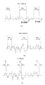
- FIGS. 1A and 1B are schematic diagrams of a surface roughness curve having the same Sm.
- finer irregularities exist in the valley period of the irregularities. Since the surface area of (b) is larger than that of (a), it is easily considered that a larger anchoring effect can be obtained.
- the index of the surface roughness representing the interval between each fine unevenness is the above-mentioned average interval S between the local peaks. S is the average of the intervals between the vertices of the individual peaks of the surface roughness curve schematically represented in FIG. Therefore, it is more important to appropriately control Rz and S.
- Patent Document 5 Japanese Patent Laid-Open No. 2011-219790 proposes a copper foil for a copper clad laminate in which the range of Rz and S is defined, and measurement is performed using a violet laser having a wavelength of 408 nm. S of the roughened copper foil particles is controlled to 210 nm or less. And since the intervals of the roughening particles are close, there are many roughening particles per unit area. For this reason, the adhesion surface area with the resin substrate is increased, and an efficient anchoring effect is obtained. It is marked as preferred.
- Patent Document 5 does not discuss the adhesiveness between the copper foil and the resin via the adhesive, and the range of Rz and S of the copper foil described in the literature is the adhesion with the adhesive. The present inventor has found a problem that when considering, S is too small to obtain sufficient adhesion.
- the present invention has been created in view of the above circumstances, and an object of the present invention is to provide a metal foil having excellent adhesion to an adhesive. Another object of the present invention is to provide a laminate of the metal foil and the resin having high adhesiveness bonded through an adhesive. Furthermore, this invention makes it another subject to provide the solar cell back surface protection sheet or solar cell back surface wiring sheet provided with the said laminated body.
- the inventor has found that the ten-point average roughness Rz on the bonding surface with the adhesive is in the range of 2.0 ⁇ m or more and 6.0 ⁇ m or less, and the ratio with the average interval S of the local peaks ( It has been found that a metal foil having Rz / S) in the range of 2.0 or more and 6.0 or less is excellent in adhesiveness with an adhesive.
- At least one surface has a ten-point average roughness Rz of 2.0 ⁇ m or more and 6.0 ⁇ m or less, and the local summit A metal foil having a ratio (Rz / S) with an average interval S of 2.0 or more and 6.0 or less.
- the metal foil is a copper foil.
- the average distance S between the local peaks is not less than 0.5 ⁇ m and not more than 3.0 ⁇ m.
- the ratio (Rz / Sm) of the ten-point average roughness Rz to the average interval Sm of the irregularities is 0.5 or more and 4.0 or less.
- the average interval Sm of the irregularities is 1.0 ⁇ m or more and 4.0 ⁇ m or less.
- the at least one surface has a coating layer made of a Cu—Zn alloy, a coating layer made of a Cu—Ni alloy, a coating layer made of a Co—Ni alloy, One or a plurality of surface coating layers are formed of a coating layer made of a Ni—Zn alloy and a rust-proof coating layer made of Cr oxide.
- a silane coupling agent treatment layer is formed on the surface coating layer.
- the metal foil is an electrolytic copper foil.
- the present invention is a laminated plate in which the metal foil and the resin according to the present invention are bonded together with an adhesive.
- the resin is a plastic film.
- the present invention is a wiring board in which a metal foil of a laminated board according to the present invention is partially etched to form a circuit.
- the present invention is a solar cell back surface protective sheet or solar cell back surface wiring sheet obtained by processing the laminate according to the present invention.
- the electrolyte solution containing copper and sulfuric acid contains chloride ions of 20 to 100 mg / L, gelatin of 0.2 to 6.0 mg / L, and at least one of thiourea and an active sulfur-containing substance.
- a method for producing a copper foil comprising a step of adding a total of 0.01 to 2.0 mg / L of seeds and electrodepositing copper under a current density of 10 to 90 A / dm 2 .
- the electrolyte solution containing copper and sulfuric acid contains chloride ions of 20 to 100 mg / L, gelatin of 0.2 to 6.0 mg / L, and at least one of thiourea and an active sulfur-containing substance.
- the electrolyte solution containing copper and sulfuric acid contains chloride ions of 20 to 100 mg / L, gelatin of 0.2 to 6.0 mg / L, and at least one of thiourea and an active sulfur-containing substance.
- a method for producing a copper foil comprising a surface treatment step of forming any one or a plurality of surface coating layers of an anticorrosive coating layer comprising an oxide and then forming a silane coupling agent layer on the surface coating layer is there.
- FIG. 1 Another aspect of the present invention is a method for manufacturing a laminated board including a step of bonding a copper foil and a resin manufactured by the method for manufacturing a copper foil according to the present invention through an adhesive.
- the metal foil according to the present invention has high adhesiveness with an adhesive, it exhibits excellent adhesiveness when bonded to a resin via an adhesive. Therefore, the laminate of the metal foil and the resin according to the present invention can be suitably used as, for example, a solar cell back surface protection sheet and a solar cell back surface wiring sheet.
- the metal foil used in the present invention is not particularly limited, but a copper foil can be typically used. However, it goes without saying that metal foils other than copper foil can be used if Rz and the ratio of Rz to S (Rz / S) are within the range shown in the present invention. For example, nickel foil and aluminum foil can be used. An alloy foil can also be used.
- Copper foils are roughly classified into electrolytic copper foils and rolled copper foils depending on the manufacturing method. Both are often used as circuit materials for printed wiring boards.
- the electrolytic copper foil is manufactured by electrolytically depositing copper from a copper sulfate plating bath onto a titanium or stainless steel rotating drum in a foil manufacturing process.
- the surface on the rotating drum side is generally referred to as a shiny surface (or drum surface)
- the surface in contact with the electrolyte on the opposite side is generally referred to as a mat surface (or precipitation surface or rough surface).
- a roughening treatment e.g., a rust prevention treatment, and a silane coupling agent treatment in the surface treatment step.
- Rolled copper foil is manufactured by repeating plastic working and heat treatment with a rolling roll (rolling process). Thereafter, generally, roughening treatment, rust prevention treatment, and silane coupling agent treatment are performed in the surface treatment step in the same manner as the electrolytic copper foil.
- composition of the copper foil in addition to high-purity copper such as electrolytic copper, electroless copper, tough pitch copper and oxygen-free copper, which are usually used as conductor patterns of printed wiring boards, for example, Sn-containing copper, Ag-containing copper, Cr, Zr Alternatively, a copper alloy such as a copper alloy to which Mg or the like is added, or a Corson copper alloy to which Ni or Si is added can also be used. In addition, when the term “copper foil” is used alone in this specification, a copper alloy foil is also included.
- the thickness of the copper foil that can be used in the present invention is not particularly limited, and may be appropriately adjusted to a thickness suitable for practical use. For example, it can be about 2 to 300 ⁇ m. However, when the copper foil of the present invention is also used as a circuit material, the copper foil thickness is 5 to 105 ⁇ m, preferably 12 to 70 ⁇ m, and typically about 18 to 35 ⁇ m.
- Rz on at least one surface is 2.0 ⁇ m or more and 6.0 ⁇ m or less, and the ratio of Rz to S (Rz / S) is 2.0 or more and 6.0 or less. Is one of the features.
- Rz indicates the 10-point average roughness defined by JIS B0601-1994
- S indicates the average interval S of the local peaks defined by JIS B0601-1994.
- Rz is defined to be 6.0 ⁇ m or less.
- Rz is preferably 5.5 ⁇ m or less.
- Rz is defined as 2.0 ⁇ m or more.
- Rz is preferably 2.5 ⁇ m or more, more preferably 3.0 ⁇ m or more.
- Rz / S tends to be smaller than 2.0.
- the adhesion strength with the adhesive is low. This is because the height of the unevenness is too small compared to the interval between the unevennesses, so that adhesion due to the anchoring effect (anchor effect) cannot be obtained sufficiently. Therefore, in this invention, ratio (Rz / S) with the local peak top average space
- Rz / S is preferably 2.2 or more, more preferably 3.5 or more.
- the local summit average interval S itself is indirectly defined by defining Rz and Rz / S.
- S is preferably 5 ⁇ m or more, and more preferably 1.0 ⁇ m or more.
- the upper limit of S is indirectly defined by similarly defining Rz and Rz / S, but is preferably 3.0 ⁇ m or less, and more preferably 2.5 ⁇ m or less. When S is larger than this range, the adhesion strength with the adhesive is lowered.
- the ratio of the ten-point average roughness Rz to the average interval Sm is preferably 0.5 or more and 4.0 or less. More preferably, it is 0 or more and 2.0 or less. Moreover, it is preferable that the average space
- various roughening treatments are applied to the surface of the metal foil made of Cu, Ni, Fe, Al, etc. obtained by electrolysis or rolling. Can be considered.
- a roughening treatment by electrodeposition of fine particles, chemical etching with a chemical agent, or an anodic oxidation method can be used.
- the production conditions of the foil making process it is preferable to optimize the production conditions of the foil making process.
- various additives are added to the electrolytic solution of copper sulfate to perform foil formation under predetermined electrolysis conditions.
- gelatin with glue as a representative example is 0.2 to 6.0 mg / L, preferably 2.0 to 5.5 mg / L, and chloride ion is 20 to 100 mg / L, preferably 20 to Use in a concentration range of 60 mg / L.
- the liquid temperature is 40 to 70 ° C., preferably 50 to 65 ° C.
- the current density is 10 to 90 A / dm 2 , preferably 50 to 90 A / dm 2
- the linear flow rate of the electrolyte is 1.0 to 5. It is suitable to carry out in the range of 0 m / second, preferably 3.0 to 5.0 m / second.
- the sulfuric acid concentration in the electrolytic solution is not limited, but is preferably 50 to 150 g / L, and preferably 80 to 120 g in order to increase the conductivity of the electrolytic solution to lower the electrolytic voltage and reduce power consumption. / L is more preferable.
- the copper concentration in the electrolytic solution is not limited, but is preferably 50 to 150 g / L, and more preferably 80 to 120 g / L in order to improve productivity during commercial production.
- the surface of the metal foil according to the present invention may be further subjected to various heat and rust preventive surface treatments or silane coupling agent treatments for the purpose of preventing oxidation discoloration of the metal foil and improving adhesion strength with the adhesive.
- various heat and rust preventive surface treatments or silane coupling agent treatments for the purpose of preventing oxidation discoloration of the metal foil and improving adhesion strength with the adhesive.
- a Cu—Zn alloy, a Cu—Ni alloy, a Ni—Co alloy, a Ni—Zn alloy, a Cr oxide is provided on a surface that satisfies at least the above-described surface roughness definition. Any one or more of the coating treatment layers made of may be laminated in combination.
- a coating treatment layer made of a Cu—Zn alloy is formed and a coating treatment layer made of a Ni—Zn alloy is laminated thereon, a coating treatment layer of a Cu—Zn alloy is formed, and a Cr oxide is formed thereon.
- a coating treatment layer made of a Cu—Zn alloy is formed, and a coating treatment layer made of a Ni—Zn alloy and a coating treatment layer made of a Cr oxide are sequentially laminated thereon, A case where a coating treatment layer made of a Ni—Zn alloy is formed and a coating treatment layer made of Cr oxide is formed thereon is exemplified.
- the total thickness of the coating treatment layer is preferably in a range that does not change Rz and Rz / S obtained in the foil-making process, and the coating amount of the whole coating treatment layer is preferably 0.01 to 10 mg / dm 2 , more preferably It is preferable that the amount be in the range of 0.1 to 6.0 mg / dm 2 , more preferably 1.0 to 5.0 mg / dm 2 .
- surface coating with a silane coupling agent may be performed on the coating treatment layer.
- the surface coating layer by the silane coupling agent is effective because the metal (copper foil) surface and the organic material (adhesive) surface are cross-linked and the mutual adhesion is improved.
- the silane coupling agent layer usually has a thickness of several to several tens of atoms and is so thin that it does not greatly change the values of Rz and Rz / S of the copper foil.
- the metal foil according to the present invention exhibits excellent adhesiveness with the adhesive by having the specific surface roughness described above.
- the adhesive used for laminating the metal foil and the resin is not limited, but the effect is high for, for example, an epoxy resin adhesive, a urethane resin adhesive, and a polyester resin adhesive.
- the adhesive strength of the polyimide adhesive is high even in conventional copper foil, so that the excellent adhesive strength of the present invention is exhibited significantly, At the time of joining with an adhesive other than the polyimide adhesive.
- the metal foil according to the present invention can form a laminate by being bonded to a resin via an adhesive.
- a copper foil may be used as the metal foil to make a copper-clad laminate by thermocompression bonding with a resin, particularly an insulating thermosetting resin.
- the material of the resin is not limited, but fluorine-containing resins such as polyvinyl fluoride (PVF), polyvinylidene fluoride (PVDF), polytetrafluoroethylene (PTFE), vinyl acetate resin, polyethylene terephthalate (PET), Polyester resins such as polybutylene terephthalate (PBT) and polyethylene naphthalate (PEN), polyolefin resins such as polypropylene, polyethylene, and polyphenylene sulfide (PPS) can be appropriately selected and used.
- the insulating thermosetting resin include, but are not limited to, epoxy resins and bismaleimide-triazine resins. Of course, it can also be bonded to polyimide.
- the thickness of the resin is not particularly limited and may be appropriately changed depending on the application. However, the thickness may be as flexible as a plastic film, for example, 10 to 1000 ⁇ m.
- the laminated board can be processed into a wiring board in which a circuit is formed by partially etching a metal foil, and can be used as a printed wiring board or a solar cell backside wiring sheet.
- the laminated plate can be processed to form a solar cell back surface protective sheet.
- Electrodeposition was carried out on a stainless steel cylindrical cathode under the electrolytic solution and electrolysis conditions shown below to obtain a copper foil having a predetermined thickness.
- an electrolytic copper foil having a thickness of 35 ⁇ m (however, Example 11 was an aluminum foil).
- Example 11 an aluminum foil having a thickness of 20 ⁇ m obtained by rolling was used as a metal foil other than a copper foil.
- Rz of the surface to be bonded to the adhesive was measured with a surf coder SE-3C manufactured by Kosaka Laboratory, and was 1.0 ⁇ m before the surface treatment.
- the purpose of the first stage roughening treatment is to generate nuclei of roughened particles on the surface of the metal foil by electrodepositing Cu fine particles at a current density exceeding the limit current density of copper ion diffusion on the outermost surface of the metal foil. It is.
- Liquid temperature 20-50 ° C
- Current density 20 to 100 A / dm 2
- Energizing time 1 to 10 seconds
- the purpose of the second stage roughening treatment is to grow the roughened particle nuclei by applying smooth plating on the nuclei of the coarsened particles generated in the first stage roughening treatment, and to obtain a roughened particle having a predetermined size.
- Cu as Cu 2+
- 20-60g / L H 2 SO 4 50 to 150 g / L
- Liquid temperature 30-60 ° C
- Current density 1 to 50 A / dm 2
- Energizing time 1 to 10 seconds
- (A) Cu—Zn alloy plating treatment (electrolyte composition, pH) NaCN: 10-30g / L NaOH: 40-100 g / L Cu (CN) 2 : 60 to 120 g / L Zn (CN) 2 : 1 to 10 g / L pH: 10-13 (Electrolysis conditions) Liquid temperature: 50-80 ° C Current density: 10 A / dm 2 Plating time: 4 seconds Coating amount: 5.0 mg / dm 2 (B) Ni—Zn alloy plating treatment (electrolyte composition, pH) Zn (as Zn 2+ ): 12 to 25 g / L Ni (as Ni 2+ ): 1-8g / L pH: 2.0 to 4.0 (Electrolysis conditions) Liquid temperature: 25-50 ° C Current density: 10 A / dm 2 Plating time: 2 seconds Coating amount: 1.5 mg / dm 2 (C) Cu-Ni alloy plating treatment (electrolyt
- Silane Coupling Agent Treatment A 0.2 vol% solution of 3-glycidoxypropyltriethoxysilane was sprayed and then dried in air at a temperature of 100 ° C. or higher for 1 to 10 seconds.
- the ten-point average roughness Rz, local peak average interval S, and average interval Sm of irregularities of the mat surface of the metal foil thus prepared were measured.
- Ten-point average roughness Rz was measured with a surf coder SE-3C manufactured by Kosaka Laboratory.
- the local peak top average interval S and the uneven average interval Sm were measured using VK-8510 manufactured by Keyence Corporation.
- the measurement method used was a line roughness-JIS94 mode. The measurement results are shown in Table 1.
- a laminated sheet of the metal foil and the plastic film was produced according to the following procedure.
- Plastic film In Examples 1 to 9 and 11 and Comparative Examples 1 to 4, Lumirror (thickness: 200 ⁇ m) manufactured by Toray Industries, Inc. was used as a polyethylene terephthalate (PET) film.
- PET polyethylene terephthalate
- the adhesive used was a mixture of Toyo Morton Co., Ltd .: two-component mixed adhesive (main agent: polyester polyol AD-76P1) / (curing agent TCS-4277) and ethyl acetate.
- the PET film coated with the adhesive was heated in a dry air atmosphere at 90 ° C. for 3 minutes to volatilize the solvent.
- (Lamination method) The surface coating treated surface of the metal foil and the adhesive coated surface of the PET film were pressure-bonded using a rubber roller to form a laminated sheet of the metal foil and the PET film.
- Example 10 and Comparative Example 5 a polyimide resin is used as a resin constituting the laminate and an adhesive, and a laminated sheet is obtained by thermocompression bonding with a hot press machine at a lamination temperature of 240 ° C. and a pressure of 2.5 Mpa. Produced.
- the metal foil on the produced laminated sheet was etched using an iron chloride-hydrochloric acid etching solution to obtain a circuit wiring sheet.
- the circuit width was 10 mm for measuring the adhesion strength described below.
- Adhesion strength measurement The adhesion strength between the metal foil and the adhesive was measured using the 90 degree peel strength method specified in JIS-C6481. For the measurement, an autograph AGS-J manufactured by Shimadzu Corporation was used. The measurement results are shown in Table 1.
- Example 1 to 11 In Examples 1 to 11, the ten-point average roughness is 2.6 to 5.6 ⁇ m, the local peak top average interval S is 1.0 to 1.3 ⁇ m, and the Rz / S ratio is 2.2 to 5.5. became.
- the adhesion strength between the copper foil and the aluminum foil and the adhesive is 0.45 to 0.72 kN / m, which is sufficient.
- Comparative Example 1 In Comparative Example 1, the foil was made without adding thiourea into the electrolytic solution in the foil making process, and then the copper foil mat surface was subjected to roughening treatment, Cu—Zn alloy plating treatment, chromate treatment, and silane coupling agent. Processing is performed in order. The difference from Example 1 is that thiourea is not added and a roughening treatment is performed in the foil-making process. Since thiourea is not added to the electrolytic solution in the foil-making process, the surface roughness Rz is larger than 6.0 ⁇ m, and Rz / S is also larger than 6.0. The adhesion strength between the copper foil and the adhesive was 0.40 kN / m. Moreover, many bubbles existed at the interface between the copper foil and the adhesive.
- Comparative Example 2 In Comparative Example 2, after the foil was made without adding glue to the electrolytic solution in the foil making process, the matte surface of the copper foil was subjected to Ni—Zn alloy plating treatment, chromate treatment and silane coupling agent treatment in this order. It is. The difference from Example 5 is that no glue is added in the foil-making process. When no glue was added to the electrolytic solution in the foil making process, Rz was smaller than 2.0 ⁇ m and Rz / S was smaller than 2.0. The adhesion strength between the copper foil and the adhesive was 0.20 kN / m.
- Comparative Example 3 In Comparative Example 3, after the foil was made without adding chloride ions to the electrolytic solution in the foil making process, the copper foil mat surface was sequentially subjected to Cu—Zn alloy plating treatment, chromate treatment, and silane coupling agent treatment. It is a thing. The difference from Example 1 is that chloride ions are not added in the foil-making process. When chloride ions are not added to the electrolytic solution in the foil-making process, Rz is in the range of 2.0 ⁇ m to 6.0 ⁇ m, but Rz / S is smaller than 2.0, and sufficient adhesion strength is obtained. Absent. The adhesion strength between the copper foil and the adhesive was 0.35 kN / m.
- Comparative Example 4 In Comparative Example 4, the current density in the foil making process was 110 A / dm 2 .
- the other production conditions are the same as in Example 6.
- the current density in the foil-making process is higher than 90 A / dm 2 , the mat surface unevenness shape changes, and Rz becomes larger and S becomes smaller than the example using the current density of 40 to 80 A / dm 2 .
- Rz was in the range of 2.0 to 6.0 ⁇ m, but Rz / S was larger than 6.0.
- bubbles were observed at the interface between the copper foil and the adhesive.
- the adhesion strength between the copper foil and the adhesive was 0.41 kN / m.
- Comparative Example 5 the resin that is bonded to the copper foil via an adhesive is a polyimide resin, and the other methods for manufacturing the copper foil are the same as in Comparative Example 2.
- Rz is smaller than 2.0 ⁇ m and Rz / S is smaller than 2.0.
- the adhesion strength between the copper foil and the adhesive was higher than when a PET film was used, and was 0.40 kN / m.
- Examples 1 to 11 have adhesive adhesive strengths of 0.45 to 0.72 kN / m, while Comparative Examples 1 to 5 have 0.20 to 0.41 kN / m. It was confirmed that the present invention is effective in improving the adhesiveness of the adhesive.
Landscapes
- Chemical & Material Sciences (AREA)
- Engineering & Computer Science (AREA)
- Metallurgy (AREA)
- Chemical Kinetics & Catalysis (AREA)
- Electrochemistry (AREA)
- Materials Engineering (AREA)
- Organic Chemistry (AREA)
- Microelectronics & Electronic Packaging (AREA)
- Manufacturing & Machinery (AREA)
- Laminated Bodies (AREA)
- Parts Printed On Printed Circuit Boards (AREA)
- Electroplating Methods And Accessories (AREA)
- Manufacturing Of Printed Wiring (AREA)
Abstract
接着剤との密着性に優れた金属箔を提供する。少なくとも一方の面において、十点平均粗さRzが2.0μm以上6.0μm以下であり、且つ、これと局部山頂の平均間隔Sとの比(Rz/S)が2.0以上6.0以下である金属箔。
Description
本発明はプリント配線板用の金属箔に関する。また、本発明は金属箔と樹脂との積層体、とりわけ太陽電池裏面保護シート及び太陽電池裏面配線シートとして好適な積層体に関する。
従来、金属箔と樹脂を張り合わせた積層体の工業的用途として代表的なものに、フレキシブルプリント配線板用の銅張積層板があり、樹脂としてはポリイミド系材料が、金属箔としては銅箔が主に使用されていた。こうした技術に加えて近年では、銅箔の良好な電気伝導性・熱伝導性を利用した新しい工業的用途として、銅箔とポリイミド以外の様々な樹脂とを接着剤を介して接着し、シート状の構造材料、回路材料又は放熱材料として使用する技術が研究・開発されている。
このような技術として、例えば特許文献1(特開2009-170771号公報)に示されるように、太陽電池裏面保護シートの熱伝導性を向上させることを目的として、銅箔の両面にプラスティックフィルムを積層した構造の太陽電池裏面保護シートが提案されている。
また、例えば特許文献2(特開2011-061151号公報)に示されるように、太陽電池裏面保護シート中の銅箔が回路状にパターン加工されており、該パターン部と太陽電池セル裏面に設けられた端子部とが接続されることによって配線材としても機能する太陽電池裏面配線シートが開発されている。
一方で、銅箔は従来、主としてプリント配線板の回路材料として使用されてきた。銅箔と熱硬化性絶縁樹脂とを当該樹脂のガラス転移温度以上の高温で熱圧着させて銅張積層板とした後に、エッチングにより銅箔面に導体パターンを形成するという工程を経て製造されるのが一般的である。銅箔と熱硬化性絶縁樹脂との密着性を向上させる技術として、粗化処理と呼ばれる銅箔表面に凹凸を形成する表面処理を施すことが一般に行われている。例えば電解銅箔の粗面(析出面)に硫酸銅酸性めっき浴を用いて、樹枝状又は小球状に銅粒子を多数電着せしめて微細な凹凸を形成し、投錨効果(アンカー効果とも言う)によって密着性を改善させる方法がある。粗化処理後には密着強度を更に向上させるためにクロメート処理によるCr酸化物被膜形成やシランカップリング剤による表面処理等が一般的に行われている。
従来のプリント配線板用銅箔において、表面粗さに着目して銅箔と樹脂との接着性を向上することを狙った技術は多いが、銅箔の表面粗さを表す指標は従来、JIS B0601-1994で規定される十点平均粗さRzであり、熱硬化性樹脂との接着面のRzを制御することで当該樹脂との密着性を得る技術が多数提案されている。例えば、特許文献3(特開2005-48269号公報)などが該当する。
しかし、投錨効果による接着の本質を考えた場合、銅箔の表面積を対象接着物に対して最適化することこそが最も重要である。このことから、銅箔と接着剤の密着性を議論するには銅箔の表面凹凸の高さを表すRzを制御するだけでは不十分であり、凹凸の間隔も合わせて考慮する必要がある。一般に、凹凸の高低差が大きい、つまりRzが大きいほど、また凹凸の間隔が小さいほど表面積は大きくなる。凹凸の間隔を表す指標として代表的なものとして、JIS B0601-1994で規定される凹凸の平均間隔Smと局部山頂の平均間隔Sがある。
例えば、特許文献4(特開2011-216598号公報)には、Rzに加えSmを制御し、RzとSmの比(Rz/Sm)が1.5~3.5の範囲にある金属箔と熱可塑性液晶ポリマーフィルムを積層して得た高周波回路基板が提案されており、これにより金属箔(実施例においては市販の銅箔)と液晶ポリマーとの高い密着性を得ることができるとされている。特許文献5(特開2011-219790号公報)には、RzとSの範囲が規定された銅張積層板用銅箔が提案されており、波長408nmのバイオレットレーザーを使用して測定した銅箔粗化粒子のSが210nm以下であると記されている。
このように、プリント配線板用の銅箔については、樹脂との接着性を高めるために表面粗さの最適化が模索されてきた。しかしながら、従来プリント配線板用に使用されてきた粗化処理銅箔を、接着剤を介して樹脂と積層する場合、銅箔と接着剤の間に十分な密着性が得られないばかりでなく、当該積層シートが高温・高湿条件下に長時間置かれるとその密着性が大きく低下するという問題があった。さらに、接着剤の厚みが不必要に厚くなって不経済となる問題もある。
こうした問題が起こる原因としては、微細な凹凸をもつ銅箔表面と接着剤とが十分な接触面積で密着していないことが考えられる。特許文献4(特開2005-48269号公報)ではRzに加えてSmを制御しているが、Rzに加えSmを制御することは銅箔と接着剤及び樹脂との接着の本質を完全に説明したとは言えない。なぜなら、Smとは凹凸の山谷周期の平均値を表すに過ぎず、その周期の中に多数存在する微細な凹凸の存在が考慮されていないからである。
このことは図1により理解される。図1の(a)と(b)は同一のSmを持つ表面粗さ曲線の模式図であるが、(b)では凹凸の山谷周期の中にさらに細かい凹凸が存在する。(b)の方が(a)よりも表面積が大きいため、より大きな投錨効果を得られることは容易に考えられる。細かい凹凸ひとつひとつの間隔を表す表面粗さの指標は前述の局部山頂の平均間隔Sである。Sとは、図1の(c)に模式的に表される表面粗さ曲線の個々の山の頂点の間隔の平均である。したがって、RzとSを適切に制御することがより重要である。
この点、特許文献5(特開2011-219790号公報)には、RzとSの範囲が規定された銅張積層板用銅箔が提案されており、波長408nmのバイオレットレーザーを使用して測定した銅箔粗化粒子のSを210nm以下に制御している。そして、粗化粒子の間隔が密であるため、単位面積あたりの粗化粒子が多く、このため、樹脂基板との接着表面積が増え、効率的な投錨効果が得られることから、Sは小さいほど好ましいであると記されている。しかし、特許文献5では、接着剤を介した銅箔と樹脂の接着性を議論しているわけではなく、当該文献に記載される銅箔のRz及びSの範囲は、接着剤との接着を考える際にはSが小さすぎて十分な密着性が得られないという問題を本発明者は見出した。
本発明は上記事情に鑑みて創作されたものであり、接着剤との密着性に優れた金属箔を提供することを課題の一つとする。また、本発明は接着剤を介して接着された、密着性の高い前記金属箔と樹脂との積層体を提供することを別の課題の一つとする。更に、本発明は前記積層体を備えた太陽電池裏面保護シート又は太陽電池裏面配線シートを提供することを更に別の課題の一つとする。
本発明者は、鋭意研究の結果、接着剤との接着面における十点平均粗さRzが2.0μm以上6.0μm以下の範囲内にあり、且つ、局部山頂の平均間隔Sとの比(Rz/S)が2.0以上6.0以下の範囲内にある金属箔が接着剤との密着性に優れることを見出した。
本発明は上記知見に基づいて完成されたものであり、一側面において、少なくとも一方の面において、十点平均粗さRzが2.0μm以上6.0μm以下であり、且つ、これと局部山頂の平均間隔Sとの比(Rz/S)が2.0以上6.0以下である金属箔である。
本発明に係る金属箔の一実施形態においては、金属箔が銅箔である。
本発明に係る金属箔の別の一実施形態においては、局部山頂の平均間隔Sが0.5μm以上3.0μm以下である。
本発明に係る金属箔の更に別の一実施形態においては、凹凸の平均間隔Smに対する十点平均粗さRzの比(Rz/Sm)が0.5以上4.0以下である。
本発明に係る金属箔の更に別の一実施形態においては、凹凸の平均間隔Smが1.0μm以上4.0μm以下である。
本発明に係る金属箔の更に別の一実施形態においては、前記少なくとも一方の面において、Cu-Zn合金からなる被覆層、Cu-Ni合金からなる被覆層、Co-Ni合金からなる被覆層、Ni-Zn合金からなる被覆層、Cr酸化物からなる防錆被覆層のうち何れか一つ又は複数の表面被覆層が形成されている。
本発明に係る金属箔の更に別の一実施形態においては、表面被覆層の上に、シランカップリング剤処理層が形成されている。
本発明に係る金属箔の更に別の一実施形態においては、金属箔が電解銅箔である。
本発明は別の一側面において、本発明に係る金属箔と樹脂とを接着剤を介して貼り合せた積層板である。
本発明に係る積層板の一実施形態においては、樹脂がプラスティックフィルムである。
本発明は更に別の一側面において、本発明に係る積層板の金属箔が部分的にエッチングされて回路を形成している配線板である。
本発明は更に別の一側面において、本発明に係る積層板を加工して得た太陽電池裏面保護シート又は太陽電池裏面配線シートである。
本発明は更に別の一側面において、銅及び硫酸を含む電解液に塩化物イオン20~100mg/Lと、ゼラチン0.2~6.0mg/Lと、チオ尿素及び活性硫黄含有物質の少なくとも1種の合計0.01~2.0mg/Lとを添加し、電流密度10~90A/dm2の条件で銅を電着させる工程を含む銅箔の製造方法である。
本発明は更に別の一側面において、銅及び硫酸を含む電解液に塩化物イオン20~100mg/Lと、ゼラチン0.2~6.0mg/Lと、チオ尿素及び活性硫黄含有物質の少なくとも1種の合計0.01~2.0mg/Lとを添加し、電流密度10~90A/dm2の条件で銅を電着させて未処理銅箔を得る製箔工程と、前記未処理銅箔の少なくとも一方の面にCu-Zn合金からなる被覆層、Cu-Ni合金からなる被覆層、Co-Ni合金からなる被覆層、Ni-Zn合金からなる被覆層、Cr酸化物からなる防錆被覆層のうち何れか一つ又は複数の表面被覆層を形成した後、前記表面被覆層上にシランカップリング剤層を形成する表面処理工程を含む銅箔の製造方法である。
本発明は更に別の一側面において、銅及び硫酸を含む電解液に塩化物イオン20~100mg/Lと、ゼラチン0.2~6.0mg/Lと、チオ尿素及び活性硫黄含有物質の少なくとも1種の合計0.01~2.0mg/Lとを添加し、電流密度10~90A/dm2の条件で銅を電着させて未処理銅箔を得る製箔工程と、前記未処理銅箔の少なくとも一方の面に粗化処理を行った後にCu-Zn合金からなる被覆層、Cu-Ni合金からなる被覆層、Co-Ni合金からなる被覆層、Ni-Zn合金からなる被覆層、Cr酸化物からなる防錆被覆層のうち何れか一つ又は複数の表面被覆層を形成し、次いで前記表面被覆層上にシランカップリング剤層を形成する表面処理工程を含む銅箔の製造方法である。
本発明は更に別の一側面において、本発明に係る銅箔の製造方法によって製造された銅箔と樹脂とを接着剤を介して貼り合わせる工程を含む積層板の製造方法である。
本発明に係る金属箔は接着剤との密着性が高いので、接着剤を介して樹脂と接着したときに優れた密着性を示す。そのため、本発明に係る金属箔と樹脂の積層体は例えば太陽電池裏面保護シート及び太陽電池裏面配線シートとして好適に使用可能である。
本発明において用いられる金属箔としては、特に限定されないが、典型的には銅箔を用いることができる。ただし、Rz、及びRzとSの比(Rz/S)が本発明で示される範囲内にあるならば、銅箔以外の金属箔を用いることができるのは言うまでもない。例えば、ニッケル箔、アルミ箔を使用できる。また、合金箔を用いることもできる。
銅箔は、その製造方法の違いによって電解銅箔と圧延銅箔に大別される。どちらもプリント配線板の回路材料として使用されることが多い。一般的には、電解銅箔は製箔工程において硫酸銅めっき浴からチタンあるいはステンレス鋼製の回転ドラム上に銅を電解析出して製造される。この時、回転ドラム側の面をシャイニー面(又はドラム面)、その反対側の電解液に接していた面をマット面(又は析出面、粗面)と呼称するのが一般的である。その後、樹脂との密着強度を向上させるために、表面処理工程において一般的にはどちらか一方あるいは両方の面に粗化処理、防錆処理、シランカップリング剤処理が施される。
圧延銅箔は圧延ロールによる塑性加工と熱処理を繰り返して製造される(圧延工程)。その後、一般的には電解銅箔と同様に表面処理工程で粗化処理、防錆処理、シランカップリング剤処理が施される。
銅箔の組成としてはプリント配線板の導体パターンとして通常使用される電解銅、無電解銅、タフピッチ銅や無酸素銅といった高純度の銅の他、例えばSn入り銅、Ag入り銅、Cr、Zr又はMg等を添加した銅合金、Ni及びSi等を添加したコルソン系銅合金のような銅合金も使用可能である。なお、本明細書において用語「銅箔」を単独で用いたときには銅合金箔も含むものとする。
本発明に用いることのできる銅箔の厚さについても特に制限はなく、実用に適した厚さに適宜調節すればよい。例えば、2~300μm程度とすることができる。但し、本発明の銅箔を回路材料としても使用する場合には銅箔厚みは5~105μm、好ましくは12~70μmであり、典型的には18~35μm程度である。
本発明に係る金属箔は、少なくとも一方の面のRzが2.0μm以上6.0μm以下であり、且つ、RzとSの比(Rz/S)が2.0以上6.0以下であることを特徴の一つとする。本発明において、RzはJIS B0601-1994で規定される十点平均粗さを指し、SはJIS B0601-1994で規定される局部山頂の平均間隔Sを指す。
Rzが6.0μmよりも大きいと、銅箔表面凹凸の谷部に接着剤が入り込まず、密着強度が低下することがある。また、凹凸部により多くの接着剤を充填する必要があるために、使用する接着剤の塗布量が不必要に増して不経済となるという問題もある。そこで、Rzは6.0μm以下と規定した。Rzは好ましくは5.5μm以下である。
Rzが2.0μmよりも小さい場合も、必要十分な接着剤との密着強度が得られない。これは、金属箔と接着剤の接触面積が少ないため、投錨効果(アンカー効果)による密着が十分に得られないからである。そこで、Rzは2.0μm以上と規定した。Rzは好ましくは2.5μm以上であり、より好ましくは3.0μm以上である。
金属箔と接着剤との密着強度をさらに高めるためには、Rzの範囲のみならず、RzとSの比(Rz/S)も合わせて考慮する必要がある。従来プリント配線板用途に使用されてきた銅箔はRz/Sが6.0よりも高い傾向にある。これは、表面の水平方向の凹凸間隔が、凹凸の高さに対して小さすぎることを意味する。この場合も、接着剤が凹凸部に入り込まず、密着強度が十分に得られない。したがって、本発明においては、凹凸の水平方向の間隔を表す指標である局部山頂平均間隔Sとの比(Rz/S)を6.0以下に規定した。Rz/Sは好ましくは5.5以下である。
また、回路幅が特別に狭いプリント配線板用途に用いられる低プロファイル銅箔又はリチウムイオン電池負極集電体用の両面平滑箔では、Rz/Sが2.0よりも小さい傾向にあり、この場合も接着剤との密着強度は低い。これは、凹凸の高さが凹凸の間隔に比して小さすぎるため、投錨効果(アンカー効果)による密着が十分に得られないからである。したがって、本発明においては、凹凸の水平方向の間隔を表す指標である局部山頂平均間隔Sとの比(Rz/S)を2.0以上に規定した。Rz/Sは好ましくは2.2以上であり、より好ましくは3.5以上である。
また、局部山頂平均間隔S自体については、Rz及びRz/Sを規定することにより間接的に規定されるが、Sが小さすぎると接着剤が凹凸部に入り込めないことから、Sは0.5μm以上であることが好ましく、1.0μm以上であることがより好ましい。Sの上限についても同様にRz及びRz/Sを規定することにより間接的に規定されるが、3.0μm以下であることが好ましく、2.5μm以下であることがより好ましい。Sがこの範囲よりも大きいと接着剤との密着強度が低下する。
金属箔と接着剤との密着強度を高める上では、凹凸の平均間隔Smに対する十点平均粗さRzの比(Rz/Sm)が0.5以上4.0以下であることが好ましく、1.0以上2.0以下であることがより好ましい。また、凹凸の平均間隔Smが1.0μm以上4.0μm以下であることが好ましく、2.0μm以上3.5μm以下であることがより好ましい。但し、先述したようにこれらを規定するだけでは十分な密着強度は得られず、Rz及びRz/Sの両方を適切な範囲に調節する必要がある。SmはJIS B0601-1994で規定される凹凸の平均間隔を指す。
本発明のRz及びRz/Sの最適範囲を持つ金属箔を製造する方法としては、電解又は圧延により得られたCu、Ni、Fe、Al等からなる金属箔の表面に、種々の粗化処理を施すことが考えられる。粗化処理としては具体的に、微細粒子の電着による粗化処理、薬剤による化学的なエッチング、陽極酸化法を用いることができる。
特に、本発明のRz及びRz/Sの最適範囲を持つ銅箔を製造するためには、製箔工程の製造条件を最適化するのがよい。具体的には、硫酸銅の電解液に種々の添加剤を加え、所定の電解条件で製箔を行うことが望まれる。添加剤としては、膠を代表例とするゼラチンを0.2~6.0mg/L、好ましくは2.0~5.5mg/L、及び塩化物イオンを20~100mg/L、好ましくは20~60mg/Lの濃度範囲で使用する。これに加えて、チオ尿素及び活性硫黄含有物質の少なくとも1種の合計濃度を0.01~2.0mg/L、好ましくは0.1~1.5mg/Lとして添加することによって十点平均粗さRz及び局部山頂平均間隔Sを最適な範囲に調整することができる。電解条件としては、液温を40~70℃、好ましくは50~65℃、電流密度10~90A/dm2、好ましくは50~90A/dm2、電解液の線流速を1.0~5.0m/秒、好ましくは3.0~5.0m/秒の範囲で実施するのが好適である。
電解液中の硫酸濃度としては、限定的ではないが、電解液の導電率を上げて電解電圧を下げ、消費電力を削減するためには50~150g/Lとすることが好ましく、80~120g/Lとすることがより好ましい。
電解液中の銅濃度としては、限定的ではないが、商業生産時の生産性を向上するために50~150g/Lとすることが好ましく、80~120g/Lとすることがより好ましい。
電解液中の硫酸濃度としては、限定的ではないが、電解液の導電率を上げて電解電圧を下げ、消費電力を削減するためには50~150g/Lとすることが好ましく、80~120g/Lとすることがより好ましい。
電解液中の銅濃度としては、限定的ではないが、商業生産時の生産性を向上するために50~150g/Lとすることが好ましく、80~120g/Lとすることがより好ましい。
本発明に係る金属箔の表面には、更に、金属箔の酸化変色防止、接着剤との密着強度向上等の目的で各種の耐熱・防錆表面処理又はシランカップリング剤処理を施してもよい。例えば、本発明に係る金属箔の一実施形態においては、少なくとも上述した表面粗さの規定を満たす面にCu-Zn合金、Cu-Ni合金、Ni-Co合金、Ni-Zn合金、Cr酸化物からなる被覆処理層の何れか一つあるいは複数を組み合わせて積層することができる。例えば、Cu-Zn合金からなる被覆処理層を形成し、その上にNi-Zn合金からなる被覆処理層を積層する場合、Cu-Zn合金の被覆処理層を形成し、その上にCr酸化物からなる被覆処理層を積層する場合、Cu-Zn合金からなる被覆処理層を形成し、その上にNi-Zn合金からなる被覆処理層及びCr酸化物からなる被覆処理層を順に積層する場合、Ni-Zn合金からなる被覆処理層を形成し、その上にCr酸化物からなる被覆処理層を形成する場合が挙げられる。
被覆処理層全体の厚みは、製箔工程で得られたRz及びRz/Sに変化を与えない範囲が好ましく、被覆処理層全体の被覆量としては0.01~10mg/dm2、より好ましくは0.1~6.0mg/dm2、さらに好ましくは1.0~5.0mg/dm2の範囲とするのが好適である。
また、本発明に係る銅箔のさらに別の一実施形態においては、前記被覆処理層の上にシランカップリング剤による表面被覆を施してもよい。シランカップリング剤による表面被覆層は、金属(銅箔)表面と有機材料(接着剤)表面を架橋して互いの密着力を向上させるので効果的である。
シランカップリング剤層は通常、数~数十原子分の厚みを持ち、非常に薄いため銅箔のRz及びRz/Sの値を大きく変化させることはない。
本発明に係る金属箔は、上述した特定の表面粗さを有していることにより、接着剤と優れた密着性を示す。金属箔と樹脂の積層に使用される接着剤には、限定的ではないが、例えばエポキシ系樹脂接着剤、ウレタン系樹脂接着剤及びポリエステル系樹脂接着剤等に対してその効果が高い。ポリイミド系接着剤にも使用可能であるが、ポリイミド系接着剤は接着強度が従来の銅箔においても高い接着強度が得られるため、本発明の優れた接着強度が有意に発揮されるのは、ポリイミド系接着剤以外の接着剤との接合時である。
本発明に係る金属箔は、接着剤を介して樹脂と貼り合せることにより積層板を形成することができる。金属箔として銅箔を用いて樹脂、特に絶縁性熱硬化性樹脂と熱圧着させて銅張積層板とすることもできる。樹脂の素材としては、限定的ではないが、例えばポリフッ化ビニル(PVF)、ポリフッ化ビニリデン(PVDF)、ポリテトラフルオロエチレン(PTFE)等のフッ素含有樹脂、酢酸ビニル樹脂、ポリエチレンテレフタレート(PET)、ポリブチレンテレフタレート(PBT)、ポリエチレンナフタレート(PEN)等のポリエステル樹脂、ポリプロピレン、ポリエチレン、ポリフェニレンサルファイド(PPS)等のポリオレフィン樹脂等を適宜選択して使用することができる。絶縁性熱硬化性樹脂としては、限定的ではないが、エポキシ樹脂、ビスマレイミド-トリアジン樹脂等が挙げられる。当然ながら、ポリイミドと貼り合わせることもできる。
樹脂の厚みには特に制限はなく、用途に応じて適宜変更すればよいが、プラスティックフィルム程度の柔軟性のある厚み、例えば10~1000μmの厚みとすることができる。
積層板は、金属箔を部分的にエッチングすることにより回路を形成した配線板に加工することができ、プリント配線板や太陽電池裏面配線シートとして用いることができる。積層板を加工して太陽電池裏面保護シートとすることもできる。
以下に、本発明の実施例を示す。これらは本発明をより良く理解するために提供するものであり、本発明が後述の実施例に限定されることを意図するものではない。
(製箔工程)
下記に示すような電解液及び電解条件でステンレス鋼製の円柱型カソード上に電析させ、所定厚みの銅箔を得た。すべての実施例及び比較例において、厚さ35μmの電解銅箔(但し、実施例11はアルミニウム箔)とした。
下記に示すような電解液及び電解条件でステンレス鋼製の円柱型カソード上に電析させ、所定厚みの銅箔を得た。すべての実施例及び比較例において、厚さ35μmの電解銅箔(但し、実施例11はアルミニウム箔)とした。
(製箔工程の電解液組成)
Cu(Cu2+として):100g/L
H2SO4:100g/L
添加剤として、Cl(塩化物イオンとして)、膠、及びチオ尿素を表1に記載の各添加量で加えた。
Cu(Cu2+として):100g/L
H2SO4:100g/L
添加剤として、Cl(塩化物イオンとして)、膠、及びチオ尿素を表1に記載の各添加量で加えた。
(製箔工程の電解条件)
液温:57℃
電流密度:40~80A/dm2
電解液流速:4.0m/秒
液温:57℃
電流密度:40~80A/dm2
電解液流速:4.0m/秒
実施例11においては、銅箔以外の金属箔として圧延によって得られた厚さ20μmのアルミニウム箔を用いた。接着剤との貼り合わせる面のRzは小坂研究所製サーフコーダーSE-3Cにより測定して、表面処理前において1.0μmであった。
(粗化処理)
実施例6~8及び11においては、製箔工程で得られた銅箔のマット面及びアルミニウム箔の表面に、以下に示す2段階の粗化処理を施した。
実施例6~8及び11においては、製箔工程で得られた銅箔のマット面及びアルミニウム箔の表面に、以下に示す2段階の粗化処理を施した。
(1段階目の粗化処理)
1段階目の粗化処理の目的は、金属箔最表面への銅イオン拡散の限界電流密度を超える電流密度でCu微粒子を電着することによって金属箔表面に粗化粒子の核を生成させることである。
(電解液組成)
Cu(Cu2+として):10~30g/L
H2SO4:50~150g/L
As:1~2000mg/L
W:1~100mg/L
(粗化処理条件)
液温:20~50℃
電流密度:20~100A/dm2
通電時間:1~10秒
1段階目の粗化処理の目的は、金属箔最表面への銅イオン拡散の限界電流密度を超える電流密度でCu微粒子を電着することによって金属箔表面に粗化粒子の核を生成させることである。
(電解液組成)
Cu(Cu2+として):10~30g/L
H2SO4:50~150g/L
As:1~2000mg/L
W:1~100mg/L
(粗化処理条件)
液温:20~50℃
電流密度:20~100A/dm2
通電時間:1~10秒
(2段階目の粗化処理)
2段階目の粗化処理の目的は、1段階目の粗化処理で生成した粗化粒子の核の上に平滑なめっきを施すことによって粗化粒子核を成長させ、所定の大きさの粗化粒子とすることである。
(電解液組成)
Cu(Cu2+として):20~60g/L
H2SO4:50~150g/L(粗化処理条件)
液温:30~60℃
電流密度:1~50A/dm2
通電時間:1~10秒
2段階目の粗化処理の目的は、1段階目の粗化処理で生成した粗化粒子の核の上に平滑なめっきを施すことによって粗化粒子核を成長させ、所定の大きさの粗化粒子とすることである。
(電解液組成)
Cu(Cu2+として):20~60g/L
H2SO4:50~150g/L(粗化処理条件)
液温:30~60℃
電流密度:1~50A/dm2
通電時間:1~10秒
(表面処理工程)
実施例1~8及び10~11においては、製箔工程で得られた銅箔のマット面(粗面、析出面)又はアルミニウム箔(実施例11)の片面上に、以下に示す表面被覆処理(a)、(b)、(c)、(d)、(e)のうち何れか1つ又は複数を選択し処理した。各実施例で適用した表面処理の組み合わせを表1に示す。各表面被覆処理層の被覆量は表面被覆層を希硝酸により溶解した後、溶解液中の被覆処理層成分元素の濃度をICP-AES法によって測定して算出した。
(a)Cu-Zn合金めっき処理
(電解液組成、pH)
NaCN :10~30g/L
NaOH :40~100g/L
Cu(CN)2 :60~120g/L
Zn(CN)2:1~10g/L
pH:10~13
(電解条件)
液温:50~80℃
電流密度:10A/dm2
めっき時間:4秒
被覆量:5.0mg/dm2
(b)Ni-Zn合金めっき処理
(電解液組成、pH)
Zn(Zn2+として):12~25g/L
Ni(Ni2+として):1~8g/L
pH:2.0~4.0
(電解条件)
液温:25~50℃
電流密度:10A/dm2
めっき時間:2秒
被覆量:1.5mg/dm2
(c)Cu-Ni合金めっき処理
(電解液組成、pH)
Cu(Cu2+として):0.01~5.0g/L
Ni(Ni2+として):5~25g/L
pH:2.0~4.0
(電解条件)
液温:25~50℃
電流密度:5A/dm2
めっき時間:2秒
被覆量:1.0mg/dm2
(d)Co-Ni合金めっき処理
(電解液組成、pH)
Co(Co2+として):0.1~6.0g/L
Ni(Ni2+として):5~20g/L
pH:2.0~4.0
(電解条件)
液温:25~50℃
電流密度:5A/dm2
めっき時間:3秒
被覆量:3.0mg/dm2
(e)電解クロメート処理
(電解液組成、pH)
K2Cr2O7:2.0~6.0g/L
Zn(Zn2+として):0~0.5g/L
Na2SO4:5~15g/L
pH:3.5~5.0
(電解条件)
液温:20~60℃
電流密度:2.0A/dm2
めっき時間:2秒
被覆量:0.15mg/dm2
最後に、前記被覆処理層の上に以下に示すシランカップリング剤処理を行った。
シランカップリング剤処理
3-グリシドキシプロピルトリエトキシシランの0.2vol%溶液をスプレー塗布後、気温100℃以上の空気中で1~10秒間乾燥させた。
シランカップリング剤処理
3-グリシドキシプロピルトリエトキシシランの0.2vol%溶液をスプレー塗布後、気温100℃以上の空気中で1~10秒間乾燥させた。
(表面粗さ測定)
このようにして作製した金属箔のマット面の十点平均粗さRz、局部山頂平均間隔S及び凹凸の平均間隔Smを測定した。十点平均粗さRzは小坂研究所製サーフコーダーSE-3Cにより測定した。局部山頂平均間隔S及び凹凸の平均間隔Smは(株)キーエンス製VK-8510を用いて測定した。測定方法は線粗さ-JIS94モードを使用した。測定結果を表1に示す。
このようにして作製した金属箔のマット面の十点平均粗さRz、局部山頂平均間隔S及び凹凸の平均間隔Smを測定した。十点平均粗さRzは小坂研究所製サーフコーダーSE-3Cにより測定した。局部山頂平均間隔S及び凹凸の平均間隔Smは(株)キーエンス製VK-8510を用いて測定した。測定方法は線粗さ-JIS94モードを使用した。測定結果を表1に示す。
(積層シートの製作)
さらに、作製した金属箔と接着剤との密着強度を測定するため、以下の手順で金属箔とプラスティックフィルムの積層シートを作製した。
(プラスティックフイルム)
実施例1~9及び11、比較例1~4においては、ポリエチレンテレフタレート(PET)製フィルムとして、東レ(株)製ルミラー(厚み200μm)を使用した。
(接着剤)
接着剤は、東洋モートン(株)製:2液混合型接着剤(主剤:ポリエステル系ポリオールAD-76P1)/(硬化剤TCS-4277)と酢酸エチルを混合して使用した。混合比(体積基準)は、AD-76P1:TCS-4277:酢酸エチル=7.5:1.0:6.5とした。
(接着剤塗布)
PETフィルム上に、前記接着剤を厚みが15μmになるように均一に塗布した。接着剤が塗布されたPETフィルムを90℃の乾燥空気雰囲気中で3分間加熱して溶剤を揮発させた。
(ラミネート法)
金属箔の表面被覆処理面とPETフィルムの接着剤塗布面を、ゴム製のローラーを用いて圧着し、金属箔とPETフィルムの積層シートを形成した。
(熱硬化法)
上記積層シートを100℃の乾燥空気雰囲気中で10時間加熱し、接着剤を硬化させた。
実施例10及び比較例5においては、積層体を構成する樹脂及び接着剤としてポリイミド樹脂を用い、熱プレス機にて積層温度を240℃、圧力2.5Mpaの条件で熱圧着して積層シートを作製した。
(配線シート製作)
作製した積層シート上の金属箔を塩化鉄-塩酸系エッチング液を用いてエッチングし、回路配線シートとした。回路幅は次に述べる密着強度測定用として10mmとした。
作製した積層シート上の金属箔を塩化鉄-塩酸系エッチング液を用いてエッチングし、回路配線シートとした。回路幅は次に述べる密着強度測定用として10mmとした。
(密着強度測定)
金属箔と接着剤の密着強度の測定をJIS-C6481に規定される90度はく離強度方法を用いて行った。測定には(株)島津製作所製オートグラフAGS-Jを使用した。測定結果を表1に示す。
金属箔と接着剤の密着強度の測定をJIS-C6481に規定される90度はく離強度方法を用いて行った。測定には(株)島津製作所製オートグラフAGS-Jを使用した。測定結果を表1に示す。
(実施例1~11)
実施例1~11において、十点平均粗さは2.6~5.6μm、局部山頂平均間隔Sは1.0~1.3μm、Rz/S比は2.2~5.5の範囲となった。銅箔及びアルミニウム箔と接着剤の密着強度は0.45~0.72kN/mとなり、十分な密着強度を有する。
実施例1~11において、十点平均粗さは2.6~5.6μm、局部山頂平均間隔Sは1.0~1.3μm、Rz/S比は2.2~5.5の範囲となった。銅箔及びアルミニウム箔と接着剤の密着強度は0.45~0.72kN/mとなり、十分な密着強度を有する。
(比較例1)
比較例1は、製箔工程の電解液中にチオ尿素を添加せずに製箔した後、銅箔のマット面に、粗化処理、Cu-Zn合金めっき処理、クロメート処理及びシランカップリング剤処理を順に施したものである。実施例1との違いは製箔工程でチオ尿素を添加していないことと粗化処理が施されていることである。製箔工程の電解液にチオ尿素が添加されていないため、表面粗さRzが6.0μmより大きく、またRz/Sも6.0より大きい。銅箔と接着剤の密着強度は0.40kN/mであった。また、銅箔と接着剤の界面には気泡が多く存在した。
比較例1は、製箔工程の電解液中にチオ尿素を添加せずに製箔した後、銅箔のマット面に、粗化処理、Cu-Zn合金めっき処理、クロメート処理及びシランカップリング剤処理を順に施したものである。実施例1との違いは製箔工程でチオ尿素を添加していないことと粗化処理が施されていることである。製箔工程の電解液にチオ尿素が添加されていないため、表面粗さRzが6.0μmより大きく、またRz/Sも6.0より大きい。銅箔と接着剤の密着強度は0.40kN/mであった。また、銅箔と接着剤の界面には気泡が多く存在した。
(比較例2)
比較例2は、製箔工程の電解液中に膠を添加せずに製箔した後、銅箔のマット面にNi-Zn合金めっき処理、クロメート処理及びシランカップリング剤処理を順に施したものである。実施例5との違いは製箔工程で膠を添加していないことである。製箔工程の電解液に膠を添加しない場合、Rzが2.0μmよりも小さく、かつRz/Sが2.0よりも小さくなった。銅箔と接着剤の密着強度は0.20kN/mであった。
比較例2は、製箔工程の電解液中に膠を添加せずに製箔した後、銅箔のマット面にNi-Zn合金めっき処理、クロメート処理及びシランカップリング剤処理を順に施したものである。実施例5との違いは製箔工程で膠を添加していないことである。製箔工程の電解液に膠を添加しない場合、Rzが2.0μmよりも小さく、かつRz/Sが2.0よりも小さくなった。銅箔と接着剤の密着強度は0.20kN/mであった。
(比較例3)
比較例3は、製箔工程の電解液中に塩化物イオンを添加せずに製箔した後、銅箔のマット面にCu-Zn合金めっき処理、クロメート処理及びシランカップリング剤処理を順に施したものである。実施例1との違いは製箔工程で塩化物イオンを添加していないことである。製箔工程の電解液に塩化物イオンを添加しない場合、Rzが2.0μm以上6.0μm以下の範囲になるが、Rz/Sが2.0よりも小さくなり、十分な密着強度が得られない。銅箔と接着剤の密着強度は0.35kN/mであった。
比較例3は、製箔工程の電解液中に塩化物イオンを添加せずに製箔した後、銅箔のマット面にCu-Zn合金めっき処理、クロメート処理及びシランカップリング剤処理を順に施したものである。実施例1との違いは製箔工程で塩化物イオンを添加していないことである。製箔工程の電解液に塩化物イオンを添加しない場合、Rzが2.0μm以上6.0μm以下の範囲になるが、Rz/Sが2.0よりも小さくなり、十分な密着強度が得られない。銅箔と接着剤の密着強度は0.35kN/mであった。
(比較例4)
比較例4は、製箔工程における電流密度を110A/dm2とした。これ以外の製造条件は実施例6と同一である。製箔工程における電流密度を90A/dm2よりも高くすると、マット面表面凹凸形状が変化し、電流密度40~80A/dm2を使用した実施例よりもRzが大きくなり、Sが小さくなる。この結果、Rzは2.0~6.0μmの範囲になるが、Rz/Sは6.0よりも大きくなった。この場合も比較例1と同様、銅箔と接着剤の界面には気泡が見られた。銅箔と接着剤の密着強度は0.41kN/mであった。
比較例4は、製箔工程における電流密度を110A/dm2とした。これ以外の製造条件は実施例6と同一である。製箔工程における電流密度を90A/dm2よりも高くすると、マット面表面凹凸形状が変化し、電流密度40~80A/dm2を使用した実施例よりもRzが大きくなり、Sが小さくなる。この結果、Rzは2.0~6.0μmの範囲になるが、Rz/Sは6.0よりも大きくなった。この場合も比較例1と同様、銅箔と接着剤の界面には気泡が見られた。銅箔と接着剤の密着強度は0.41kN/mであった。
(比較例5)
比較例5は、銅箔と接着剤を介して接着する樹脂をポリイミド樹脂としたもので、それ以外の銅箔の製造方法は比較例2と同一である。Rzが2.0μmよりも小さく、かつRz/Sが2.0よりも小さくなる。銅箔と接着剤の密着強度はPETフィルムを用いたときよりも高くなり、0.40kN/mであった。
比較例5は、銅箔と接着剤を介して接着する樹脂をポリイミド樹脂としたもので、それ以外の銅箔の製造方法は比較例2と同一である。Rzが2.0μmよりも小さく、かつRz/Sが2.0よりも小さくなる。銅箔と接着剤の密着強度はPETフィルムを用いたときよりも高くなり、0.40kN/mであった。
以上に示すように、実施例1~11は接着剤密着強度が0.45~0.72kN/mであるのに対し、比較例1~5は0.20~0.41kN/mであり、本発明は接着剤の密着性向上に効果がある事が確認された。

Claims (16)
- 少なくとも一方の面において、十点平均粗さRzが2.0μm以上6.0μm以下であり、且つ、これと局部山頂の平均間隔Sとの比(Rz/S)が2.0以上6.0以下である金属箔。
- 金属箔が銅箔である請求項1に記載の金属箔。
- 局部山頂の平均間隔Sが0.5μm以上3.0μm以下である請求項1又は2に記載の金属箔。
- 凹凸の平均間隔Smに対する十点平均粗さRzの比(Rz/Sm)が0.5以上4.0以下である請求項1~3の何れか一項に記載の金属箔。
- 凹凸の平均間隔Smが1.0μm以上4.0μm以下である請求項1~4の何れか一項に記載の金属箔。
- 前記少なくとも一方の面において、Cu-Zn合金からなる被覆層、Cu-Ni合金からなる被覆層、Co-Ni合金からなる被覆層、Ni-Zn合金からなる被覆層、Cr酸化物からなる防錆被覆層のうち何れか一つ又は複数の表面被覆層が形成されている請求項1~5の何れか一項に記載の金属箔。
- 表面被覆層の上に、シランカップリング剤処理層が形成されている請求項6に記載の金属箔。
- 金属箔が電解銅箔である請求項1~7の何れか一項に記載の金属箔。
- 請求項1~8の何れか一項に記載の金属箔と樹脂とを接着剤を介して貼り合せた積層板。
- 樹脂がプラスティックフィルムである請求項9に記載の積層板。
- 請求項9又は10に記載の積層板の金属箔が部分的にエッチングされて回路を形成している配線板。
- 請求項9又は10に記載の積層板を加工して得た太陽電池裏面保護シート又は太陽電池裏面配線シート。
- 銅及び硫酸を含む電解液に塩化物イオン20~100mg/Lと、ゼラチン0.2~6.0mg/Lと、チオ尿素及び活性硫黄含有物質の少なくとも1種の合計0.01~2.0mg/Lとを添加し、電流密度10~90A/dm2の条件で銅を電着させる工程を含む銅箔の製造方法。
- 銅及び硫酸を含む電解液に塩化物イオン20~100mg/Lと、ゼラチン0.2~6.0mg/Lと、チオ尿素及び活性硫黄含有物質の少なくとも1種の合計0.01~2.0mg/Lとを添加し、電流密度10~90A/dm2の条件で銅を電着させて未処理銅箔を得る製箔工程と、前記未処理銅箔の少なくとも一方の面にCu-Zn合金からなる被覆層、Cu-Ni合金からなる被覆層、Co-Ni合金からなる被覆層、Ni-Zn合金からなる被覆層、Cr酸化物からなる防錆被覆層のうち何れか一つ又は複数の表面被覆層を形成した後、前記表面被覆層上にシランカップリング剤層を形成する表面処理工程を含む銅箔の製造方法。
- 銅及び硫酸を含む電解液に塩化物イオン20~100mg/Lと、ゼラチン0.2~6.0mg/Lと、チオ尿素及び活性硫黄含有物質の少なくとも1種の合計0.01~2.0mg/Lとを添加し、電流密度10~90A/dm2の条件で銅を電着させて未処理銅箔を得る製箔工程と、前記未処理銅箔の少なくとも一方の面に粗化処理を行った後にCu-Zn合金からなる被覆層、Cu-Ni合金からなる被覆層、Co-Ni合金からなる被覆層、Ni-Zn合金からなる被覆層、Cr酸化物からなる防錆被覆層のうち何れか一つ又は複数の表面被覆層を形成し、次いで前記表面被覆層上にシランカップリング剤層を形成する表面処理工程を含む銅箔の製造方法。
- 請求項13~15の何れかに記載の製造方法によって製造された銅箔と樹脂とを接着剤を介して貼り合わせる工程を含む積層板の製造方法。
Priority Applications (3)
| Application Number | Priority Date | Filing Date | Title |
|---|---|---|---|
| KR1020147030582A KR20140141704A (ko) | 2012-03-30 | 2013-02-28 | 금속박 |
| CN201380018605.7A CN104271812B (zh) | 2012-03-30 | 2013-02-28 | 金属箔 |
| KR1020167032633A KR102095619B1 (ko) | 2012-03-30 | 2013-02-28 | 금속박 |
Applications Claiming Priority (2)
| Application Number | Priority Date | Filing Date | Title |
|---|---|---|---|
| JP2012083265A JP5858849B2 (ja) | 2012-03-30 | 2012-03-30 | 金属箔 |
| JP2012-083265 | 2012-03-30 |
Publications (1)
| Publication Number | Publication Date |
|---|---|
| WO2013146088A1 true WO2013146088A1 (ja) | 2013-10-03 |
Family
ID=49259363
Family Applications (1)
| Application Number | Title | Priority Date | Filing Date |
|---|---|---|---|
| PCT/JP2013/055572 WO2013146088A1 (ja) | 2012-03-30 | 2013-02-28 | 金属箔 |
Country Status (5)
| Country | Link |
|---|---|
| JP (1) | JP5858849B2 (ja) |
| KR (2) | KR20140141704A (ja) |
| CN (1) | CN104271812B (ja) |
| TW (1) | TWI481746B (ja) |
| WO (1) | WO2013146088A1 (ja) |
Cited By (4)
| Publication number | Priority date | Publication date | Assignee | Title |
|---|---|---|---|---|
| WO2017179416A1 (ja) * | 2016-04-14 | 2017-10-19 | 三井金属鉱業株式会社 | 表面処理銅箔、キャリア付銅箔、並びにそれらを用いた銅張積層板及びプリント配線板の製造方法 |
| JP2019210520A (ja) * | 2018-06-05 | 2019-12-12 | Jx金属株式会社 | 表面処理銅箔、銅張積層板及びプリント配線板 |
| JP2019210521A (ja) * | 2018-06-05 | 2019-12-12 | Jx金属株式会社 | 表面処理銅箔、銅張積層板及びプリント配線板 |
| EP4202086A3 (en) * | 2021-12-24 | 2023-10-18 | Circuit Foil Luxembourg | Electrolytic copper foil and secondary battery comprising the same |
Families Citing this family (9)
| Publication number | Priority date | Publication date | Assignee | Title |
|---|---|---|---|---|
| JP6650923B2 (ja) * | 2015-03-24 | 2020-02-19 | 三井金属鉱業株式会社 | キャリア付極薄銅箔、その製造方法、銅張積層板及びプリント配線板 |
| JP6023367B1 (ja) * | 2015-06-17 | 2016-11-09 | Jx金属株式会社 | キャリア付銅箔、積層体、プリント配線板の製造方法及び電子機器の製造方法 |
| JP6683507B2 (ja) * | 2015-07-22 | 2020-04-22 | サトーホールディングス株式会社 | ラベルを用いた加工物の生産を管理する方法 |
| JP6594108B2 (ja) * | 2015-08-25 | 2019-10-23 | サトーホールディングス株式会社 | ラベル、および、当該ラベルを用いた加工物の生産を管理する方法 |
| JP6605271B2 (ja) * | 2015-09-24 | 2019-11-13 | Jx金属株式会社 | 離型層付き電解銅箔、積層体、半導体パッケージの製造方法、電子機器の製造方法及びプリント配線板の製造方法 |
| JP6204430B2 (ja) * | 2015-09-24 | 2017-09-27 | Jx金属株式会社 | 金属箔、離型層付き金属箔、積層体、プリント配線板、半導体パッケージ、電子機器及びプリント配線板の製造方法 |
| JP6782116B2 (ja) * | 2016-08-02 | 2020-11-11 | 古河電気工業株式会社 | 銀被覆材料 |
| KR102098475B1 (ko) | 2018-07-06 | 2020-04-07 | 주식회사 포스코 | 내식성, 도장성이 우수한 표면처리된 Zn-Ni 합금 전기도금강판의 제조방법 |
| WO2023028983A1 (zh) * | 2021-09-03 | 2023-03-09 | 宁德时代新能源科技股份有限公司 | 金属箔及制备方法、集流体、电极、电池及用电装置 |
Citations (7)
| Publication number | Priority date | Publication date | Assignee | Title |
|---|---|---|---|---|
| JPH04501887A (ja) * | 1989-09-13 | 1992-04-02 | グールド エレクトロニクス インコーポレイテッド | 特性の調整された、印刷回路基板用の電着された箔並びにそれを製造するための方法及び電解槽溶液 |
| JPH09143785A (ja) * | 1995-09-22 | 1997-06-03 | Furukawa Circuit Foil Kk | ファインパターン用電解銅箔とその製造方法 |
| JP2001123290A (ja) * | 1999-10-27 | 2001-05-08 | Dowa Mining Co Ltd | 電解銅箔とその製造方法 |
| WO2010061736A1 (ja) * | 2008-11-25 | 2010-06-03 | 日鉱金属株式会社 | 印刷回路用銅箔 |
| JP2011127226A (ja) * | 2005-06-23 | 2011-06-30 | Jx Nippon Mining & Metals Corp | プリント配線板用銅箔 |
| WO2011078077A1 (ja) * | 2009-12-24 | 2011-06-30 | Jx日鉱日石金属株式会社 | 表面処理銅箔 |
| JP2011216598A (ja) * | 2010-03-31 | 2011-10-27 | Kuraray Co Ltd | 高周波回路基板 |
Family Cites Families (12)
| Publication number | Priority date | Publication date | Assignee | Title |
|---|---|---|---|---|
| AU7952791A (en) * | 1990-05-30 | 1991-12-31 | Gould Inc. | Electrodeposited copper foil and process for making same using electrolyte solutions having low chloride ion concentrations |
| JPH1036992A (ja) * | 1996-07-19 | 1998-02-10 | Japan Energy Corp | 電解銅箔及びその製造方法 |
| JP4419161B2 (ja) * | 1999-10-27 | 2010-02-24 | Dowaホールディングス株式会社 | 電解銅箔の製造方法 |
| JP2004226615A (ja) * | 2003-01-22 | 2004-08-12 | Ricoh Co Ltd | 現像装置およびこれを使用する画像形成装置 |
| TW200500199A (en) * | 2003-02-12 | 2005-01-01 | Furukawa Circuit Foil | Copper foil for fine patterned printed circuits and method of production of same |
| JP4172704B2 (ja) | 2003-07-31 | 2008-10-29 | 日鉱金属株式会社 | 表面処理銅箔およびそれを使用した基板 |
| JP2009170771A (ja) | 2008-01-18 | 2009-07-30 | Toppan Printing Co Ltd | 太陽電池バックシート及び太陽電池モジュール |
| JP2011061151A (ja) | 2009-09-14 | 2011-03-24 | Toppan Printing Co Ltd | 太陽電池用裏面保護シートおよびその製造方法、太陽電池モジュール |
| JP5493797B2 (ja) * | 2009-12-10 | 2014-05-14 | 富士ゼロックス株式会社 | 画像形成装置および定着装置 |
| JP5885054B2 (ja) * | 2010-04-06 | 2016-03-15 | 福田金属箔粉工業株式会社 | 銅張積層板用処理銅箔及び該処理銅箔を絶縁性樹脂基材に接着してなる銅張積層板並びに該銅張積層板を用いたプリント配線板。 |
| JP5634103B2 (ja) | 2010-04-06 | 2014-12-03 | 福田金属箔粉工業株式会社 | 銅張積層板用処理銅箔及び該処理銅箔を絶縁性樹脂基材に接着してなる銅張積層板並びに該銅張積層板を用いたプリント配線板。 |
| JP5128695B2 (ja) * | 2010-06-28 | 2013-01-23 | 古河電気工業株式会社 | 電解銅箔、リチウムイオン二次電池用電解銅箔、該電解銅箔を用いたリチウムイオン二次電池用電極、該電極を使用したリチウムイオン二次電池 |
-
2012
- 2012-03-30 JP JP2012083265A patent/JP5858849B2/ja active Active
-
2013
- 2013-02-28 CN CN201380018605.7A patent/CN104271812B/zh active Active
- 2013-02-28 KR KR1020147030582A patent/KR20140141704A/ko active Application Filing
- 2013-02-28 WO PCT/JP2013/055572 patent/WO2013146088A1/ja active Application Filing
- 2013-02-28 KR KR1020167032633A patent/KR102095619B1/ko active IP Right Grant
- 2013-03-04 TW TW102107462A patent/TWI481746B/zh active
Patent Citations (7)
| Publication number | Priority date | Publication date | Assignee | Title |
|---|---|---|---|---|
| JPH04501887A (ja) * | 1989-09-13 | 1992-04-02 | グールド エレクトロニクス インコーポレイテッド | 特性の調整された、印刷回路基板用の電着された箔並びにそれを製造するための方法及び電解槽溶液 |
| JPH09143785A (ja) * | 1995-09-22 | 1997-06-03 | Furukawa Circuit Foil Kk | ファインパターン用電解銅箔とその製造方法 |
| JP2001123290A (ja) * | 1999-10-27 | 2001-05-08 | Dowa Mining Co Ltd | 電解銅箔とその製造方法 |
| JP2011127226A (ja) * | 2005-06-23 | 2011-06-30 | Jx Nippon Mining & Metals Corp | プリント配線板用銅箔 |
| WO2010061736A1 (ja) * | 2008-11-25 | 2010-06-03 | 日鉱金属株式会社 | 印刷回路用銅箔 |
| WO2011078077A1 (ja) * | 2009-12-24 | 2011-06-30 | Jx日鉱日石金属株式会社 | 表面処理銅箔 |
| JP2011216598A (ja) * | 2010-03-31 | 2011-10-27 | Kuraray Co Ltd | 高周波回路基板 |
Cited By (6)
| Publication number | Priority date | Publication date | Assignee | Title |
|---|---|---|---|---|
| WO2017179416A1 (ja) * | 2016-04-14 | 2017-10-19 | 三井金属鉱業株式会社 | 表面処理銅箔、キャリア付銅箔、並びにそれらを用いた銅張積層板及びプリント配線板の製造方法 |
| JPWO2017179416A1 (ja) * | 2016-04-14 | 2019-02-21 | 三井金属鉱業株式会社 | 表面処理銅箔、キャリア付銅箔、並びにそれらを用いた銅張積層板及びプリント配線板の製造方法 |
| TWI711139B (zh) * | 2016-04-14 | 2020-11-21 | 日商三井金屬鑛業股份有限公司 | 表面處理銅箔、附有載體之銅箔以及使用此等之貼銅層積板及印刷配線板之製造方法 |
| JP2019210520A (ja) * | 2018-06-05 | 2019-12-12 | Jx金属株式会社 | 表面処理銅箔、銅張積層板及びプリント配線板 |
| JP2019210521A (ja) * | 2018-06-05 | 2019-12-12 | Jx金属株式会社 | 表面処理銅箔、銅張積層板及びプリント配線板 |
| EP4202086A3 (en) * | 2021-12-24 | 2023-10-18 | Circuit Foil Luxembourg | Electrolytic copper foil and secondary battery comprising the same |
Also Published As
| Publication number | Publication date |
|---|---|
| TW201343976A (zh) | 2013-11-01 |
| CN104271812B (zh) | 2016-10-05 |
| JP2013213250A (ja) | 2013-10-17 |
| CN104271812A (zh) | 2015-01-07 |
| TWI481746B (zh) | 2015-04-21 |
| KR20160137678A (ko) | 2016-11-30 |
| KR102095619B1 (ko) | 2020-03-31 |
| JP5858849B2 (ja) | 2016-02-10 |
| KR20140141704A (ko) | 2014-12-10 |
Similar Documents
| Publication | Publication Date | Title |
|---|---|---|
| JP5858849B2 (ja) | 金属箔 | |
| WO2017179416A1 (ja) | 表面処理銅箔、キャリア付銅箔、並びにそれらを用いた銅張積層板及びプリント配線板の製造方法 | |
| KR101129471B1 (ko) | 표면처리동박 및 회로기판 | |
| KR102078897B1 (ko) | 표면 처리 전해 동박, 적층판, 및 프린트 배선판 | |
| TWI704048B (zh) | 表面處理銅箔及使用其製成的覆銅積層板 | |
| WO2014196576A1 (ja) | キャリア付銅箔、銅張積層板、プリント配線板、電子機器、樹脂層、キャリア付銅箔の製造方法、及びプリント配線板の製造方法 | |
| TWI530234B (zh) | Printed wiring board with copper foil and the use of its laminated body, printed wiring board and electronic components | |
| JP7453154B2 (ja) | 表面処理銅箔、キャリア付銅箔、銅張積層板及びプリント配線板 | |
| JP2013213250A5 (ja) | ||
| JPWO2012046804A1 (ja) | 銅箔及びその製造方法、キャリア付き銅箔及びその製造方法、プリント配線板、多層プリント配線板 | |
| KR20160119875A (ko) | 수지와의 밀착성이 우수한 동박 및 그 제조 방법 그리고 그 전해 동박을 사용한 프린트 배선판 또는 전지용 부극재 | |
| JP2015124426A (ja) | 表面処理銅箔及び積層板 | |
| KR101695236B1 (ko) | 동박, 이를 포함하는 전기부품 및 전지 | |
| KR101822251B1 (ko) | 구리박, 캐리어 부착 구리박, 구리 피복 적층체, 프린트 배선판, 반도체 패키지용 회로 형성 기판, 반도체 패키지, 전자 기기, 수지 기재, 회로의 형성 방법, 세미 애디티브 공법, 프린트 배선판의 제조 방법 | |
| JP2009214308A (ja) | キャリア付き銅箔 | |
| JP2005288856A (ja) | キャリア箔付電解銅箔及びその製造方法並びにそのキャリア箔付電解銅箔を用いた銅張積層板 | |
| WO2021131359A1 (ja) | 表面処理銅箔及びその製造方法 | |
| JP2007046095A (ja) | 銅箔およびその表面処理方法 | |
| JP2010218905A (ja) | 基板用金属材料、基板用金属材料の表面粗化処理方法および基板用金属材料の製造方法 | |
| JP2004124214A (ja) | キャリア箔付電解銅箔並びにその製造方法及びそのキャリア箔付電解銅箔を用いた銅張積層板 | |
| JP4330979B2 (ja) | 表面処理電解銅箔 | |
| JP4471795B2 (ja) | 電解銅箔の製造方法およびプリント配線板 | |
| TW202244330A (zh) | 粗化處理銅箔、銅箔積層板及印刷佈線板 | |
| JP2023040316A (ja) | 表面処理金属箔及び金属張積層板 |
Legal Events
| Date | Code | Title | Description |
|---|---|---|---|
| 121 | Ep: the epo has been informed by wipo that ep was designated in this application |
Ref document number: 13770089 Country of ref document: EP Kind code of ref document: A1 |
|
| DPE1 | Request for preliminary examination filed after expiration of 19th month from priority date (pct application filed from 20040101) | ||
| NENP | Non-entry into the national phase |
Ref country code: DE |
|
| ENP | Entry into the national phase |
Ref document number: 20147030582 Country of ref document: KR Kind code of ref document: A |
|
| 122 | Ep: pct application non-entry in european phase |
Ref document number: 13770089 Country of ref document: EP Kind code of ref document: A1 |