WO2013099243A1 - 接合構造体 - Google Patents
接合構造体 Download PDFInfo
- Publication number
- WO2013099243A1 WO2013099243A1 PCT/JP2012/008324 JP2012008324W WO2013099243A1 WO 2013099243 A1 WO2013099243 A1 WO 2013099243A1 JP 2012008324 W JP2012008324 W JP 2012008324W WO 2013099243 A1 WO2013099243 A1 WO 2013099243A1
- Authority
- WO
- WIPO (PCT)
- Prior art keywords
- layer
- intermetallic compound
- electrode
- semiconductor element
- bonding
- Prior art date
Links
- 229910000765 intermetallic Inorganic materials 0.000 claims abstract description 238
- 239000004065 semiconductor Substances 0.000 claims abstract description 180
- 229910016347 CuSn Inorganic materials 0.000 claims abstract description 71
- 239000000758 substrate Substances 0.000 claims abstract description 35
- 239000000463 material Substances 0.000 claims description 123
- 229910020830 Sn-Bi Inorganic materials 0.000 claims description 113
- 229910018728 Sn—Bi Inorganic materials 0.000 claims description 113
- 238000005304 joining Methods 0.000 claims description 43
- 229910017750 AgSn Inorganic materials 0.000 claims description 20
- 229910017482 Cu 6 Sn 5 Inorganic materials 0.000 claims description 6
- 230000002250 progressing effect Effects 0.000 abstract 1
- 239000010410 layer Substances 0.000 description 500
- ORQBXQOJMQIAOY-UHFFFAOYSA-N nobelium Chemical group [No] ORQBXQOJMQIAOY-UHFFFAOYSA-N 0.000 description 49
- 238000000034 method Methods 0.000 description 41
- 230000008646 thermal stress Effects 0.000 description 23
- 150000001875 compounds Chemical class 0.000 description 22
- 230000008018 melting Effects 0.000 description 21
- 238000002844 melting Methods 0.000 description 21
- 239000000047 product Substances 0.000 description 21
- 238000000926 separation method Methods 0.000 description 18
- 238000006243 chemical reaction Methods 0.000 description 16
- 238000010438 heat treatment Methods 0.000 description 16
- 238000004519 manufacturing process Methods 0.000 description 15
- 238000009792 diffusion process Methods 0.000 description 14
- 230000035882 stress Effects 0.000 description 14
- 238000005336 cracking Methods 0.000 description 13
- 230000020169 heat generation Effects 0.000 description 13
- 230000015572 biosynthetic process Effects 0.000 description 11
- 229910052802 copper Inorganic materials 0.000 description 10
- 229910052718 tin Inorganic materials 0.000 description 10
- 239000000203 mixture Substances 0.000 description 9
- 238000001816 cooling Methods 0.000 description 8
- 239000001257 hydrogen Substances 0.000 description 8
- 229910052739 hydrogen Inorganic materials 0.000 description 8
- 238000005259 measurement Methods 0.000 description 8
- 239000012299 nitrogen atmosphere Substances 0.000 description 8
- 229910000679 solder Inorganic materials 0.000 description 8
- UFHFLCQGNIYNRP-UHFFFAOYSA-N Hydrogen Chemical compound [H][H] UFHFLCQGNIYNRP-UHFFFAOYSA-N 0.000 description 6
- 238000009713 electroplating Methods 0.000 description 6
- 229910052709 silver Inorganic materials 0.000 description 6
- 230000002950 deficient Effects 0.000 description 5
- 239000002184 metal Substances 0.000 description 5
- 229910052751 metal Inorganic materials 0.000 description 5
- 238000012986 modification Methods 0.000 description 5
- 230000004048 modification Effects 0.000 description 5
- RYGMFSIKBFXOCR-UHFFFAOYSA-N Copper Chemical compound [Cu] RYGMFSIKBFXOCR-UHFFFAOYSA-N 0.000 description 4
- 229910052797 bismuth Inorganic materials 0.000 description 4
- 230000008034 disappearance Effects 0.000 description 4
- 230000002265 prevention Effects 0.000 description 4
- 238000001771 vacuum deposition Methods 0.000 description 4
- 229910000881 Cu alloy Inorganic materials 0.000 description 3
- 238000007772 electroless plating Methods 0.000 description 3
- 230000005496 eutectics Effects 0.000 description 3
- 230000001747 exhibiting effect Effects 0.000 description 3
- 239000011888 foil Substances 0.000 description 3
- 229910005887 NiSn Inorganic materials 0.000 description 2
- 238000002441 X-ray diffraction Methods 0.000 description 2
- 238000004364 calculation method Methods 0.000 description 2
- 238000007598 dipping method Methods 0.000 description 2
- 239000006185 dispersion Substances 0.000 description 2
- 150000002431 hydrogen Chemical class 0.000 description 2
- 239000002244 precipitate Substances 0.000 description 2
- 238000007789 sealing Methods 0.000 description 2
- 239000002356 single layer Substances 0.000 description 2
- 238000003860 storage Methods 0.000 description 2
- 229910020816 Sn Pb Inorganic materials 0.000 description 1
- 229910020922 Sn-Pb Inorganic materials 0.000 description 1
- 229910008783 Sn—Pb Inorganic materials 0.000 description 1
- 238000004458 analytical method Methods 0.000 description 1
- 230000007423 decrease Effects 0.000 description 1
- 230000032798 delamination Effects 0.000 description 1
- 238000000151 deposition Methods 0.000 description 1
- 238000010586 diagram Methods 0.000 description 1
- 238000002845 discoloration Methods 0.000 description 1
- 239000007772 electrode material Substances 0.000 description 1
- 230000007613 environmental effect Effects 0.000 description 1
- 229910052737 gold Inorganic materials 0.000 description 1
- CNQCVBJFEGMYDW-UHFFFAOYSA-N lawrencium atom Chemical compound [Lr] CNQCVBJFEGMYDW-UHFFFAOYSA-N 0.000 description 1
- 238000001465 metallisation Methods 0.000 description 1
- 229910052759 nickel Inorganic materials 0.000 description 1
- 230000003647 oxidation Effects 0.000 description 1
- 238000007254 oxidation reaction Methods 0.000 description 1
- 238000004806 packaging method and process Methods 0.000 description 1
- 230000000704 physical effect Effects 0.000 description 1
Images


Classifications
-
- H—ELECTRICITY
- H01—ELECTRIC ELEMENTS
- H01L—SEMICONDUCTOR DEVICES NOT COVERED BY CLASS H10
- H01L24/00—Arrangements for connecting or disconnecting semiconductor or solid-state bodies; Methods or apparatus related thereto
- H01L24/01—Means for bonding being attached to, or being formed on, the surface to be connected, e.g. chip-to-package, die-attach, "first-level" interconnects; Manufacturing methods related thereto
- H01L24/02—Bonding areas ; Manufacturing methods related thereto
- H01L24/04—Structure, shape, material or disposition of the bonding areas prior to the connecting process
- H01L24/05—Structure, shape, material or disposition of the bonding areas prior to the connecting process of an individual bonding area
-
- B—PERFORMING OPERATIONS; TRANSPORTING
- B23—MACHINE TOOLS; METAL-WORKING NOT OTHERWISE PROVIDED FOR
- B23K—SOLDERING OR UNSOLDERING; WELDING; CLADDING OR PLATING BY SOLDERING OR WELDING; CUTTING BY APPLYING HEAT LOCALLY, e.g. FLAME CUTTING; WORKING BY LASER BEAM
- B23K35/00—Rods, electrodes, materials, or media, for use in soldering, welding, or cutting
- B23K35/02—Rods, electrodes, materials, or media, for use in soldering, welding, or cutting characterised by mechanical features, e.g. shape
- B23K35/0255—Rods, electrodes, materials, or media, for use in soldering, welding, or cutting characterised by mechanical features, e.g. shape for use in welding
- B23K35/0261—Rods, electrodes, wires
- B23K35/0272—Rods, electrodes, wires with more than one layer of coating or sheathing material
-
- B—PERFORMING OPERATIONS; TRANSPORTING
- B23—MACHINE TOOLS; METAL-WORKING NOT OTHERWISE PROVIDED FOR
- B23K—SOLDERING OR UNSOLDERING; WELDING; CLADDING OR PLATING BY SOLDERING OR WELDING; CUTTING BY APPLYING HEAT LOCALLY, e.g. FLAME CUTTING; WORKING BY LASER BEAM
- B23K35/00—Rods, electrodes, materials, or media, for use in soldering, welding, or cutting
- B23K35/22—Rods, electrodes, materials, or media, for use in soldering, welding, or cutting characterised by the composition or nature of the material
- B23K35/24—Selection of soldering or welding materials proper
- B23K35/26—Selection of soldering or welding materials proper with the principal constituent melting at less than 400 degrees C
- B23K35/264—Bi as the principal constituent
-
- B—PERFORMING OPERATIONS; TRANSPORTING
- B23—MACHINE TOOLS; METAL-WORKING NOT OTHERWISE PROVIDED FOR
- B23K—SOLDERING OR UNSOLDERING; WELDING; CLADDING OR PLATING BY SOLDERING OR WELDING; CUTTING BY APPLYING HEAT LOCALLY, e.g. FLAME CUTTING; WORKING BY LASER BEAM
- B23K35/00—Rods, electrodes, materials, or media, for use in soldering, welding, or cutting
- B23K35/22—Rods, electrodes, materials, or media, for use in soldering, welding, or cutting characterised by the composition or nature of the material
- B23K35/24—Selection of soldering or welding materials proper
- B23K35/30—Selection of soldering or welding materials proper with the principal constituent melting at less than 1550 degrees C
- B23K35/302—Cu as the principal constituent
-
- H—ELECTRICITY
- H01—ELECTRIC ELEMENTS
- H01L—SEMICONDUCTOR DEVICES NOT COVERED BY CLASS H10
- H01L23/00—Details of semiconductor or other solid state devices
- H01L23/48—Arrangements for conducting electric current to or from the solid state body in operation, e.g. leads, terminal arrangements ; Selection of materials therefor
- H01L23/488—Arrangements for conducting electric current to or from the solid state body in operation, e.g. leads, terminal arrangements ; Selection of materials therefor consisting of soldered or bonded constructions
- H01L23/492—Bases or plates or solder therefor
-
- H—ELECTRICITY
- H01—ELECTRIC ELEMENTS
- H01L—SEMICONDUCTOR DEVICES NOT COVERED BY CLASS H10
- H01L24/00—Arrangements for connecting or disconnecting semiconductor or solid-state bodies; Methods or apparatus related thereto
- H01L24/01—Means for bonding being attached to, or being formed on, the surface to be connected, e.g. chip-to-package, die-attach, "first-level" interconnects; Manufacturing methods related thereto
- H01L24/26—Layer connectors, e.g. plate connectors, solder or adhesive layers; Manufacturing methods related thereto
- H01L24/28—Structure, shape, material or disposition of the layer connectors prior to the connecting process
- H01L24/29—Structure, shape, material or disposition of the layer connectors prior to the connecting process of an individual layer connector
-
- H—ELECTRICITY
- H01—ELECTRIC ELEMENTS
- H01L—SEMICONDUCTOR DEVICES NOT COVERED BY CLASS H10
- H01L24/00—Arrangements for connecting or disconnecting semiconductor or solid-state bodies; Methods or apparatus related thereto
- H01L24/01—Means for bonding being attached to, or being formed on, the surface to be connected, e.g. chip-to-package, die-attach, "first-level" interconnects; Manufacturing methods related thereto
- H01L24/26—Layer connectors, e.g. plate connectors, solder or adhesive layers; Manufacturing methods related thereto
- H01L24/31—Structure, shape, material or disposition of the layer connectors after the connecting process
- H01L24/32—Structure, shape, material or disposition of the layer connectors after the connecting process of an individual layer connector
-
- H—ELECTRICITY
- H01—ELECTRIC ELEMENTS
- H01L—SEMICONDUCTOR DEVICES NOT COVERED BY CLASS H10
- H01L24/00—Arrangements for connecting or disconnecting semiconductor or solid-state bodies; Methods or apparatus related thereto
- H01L24/80—Methods for connecting semiconductor or other solid state bodies using means for bonding being attached to, or being formed on, the surface to be connected
- H01L24/83—Methods for connecting semiconductor or other solid state bodies using means for bonding being attached to, or being formed on, the surface to be connected using a layer connector
-
- H—ELECTRICITY
- H01—ELECTRIC ELEMENTS
- H01L—SEMICONDUCTOR DEVICES NOT COVERED BY CLASS H10
- H01L2224/00—Indexing scheme for arrangements for connecting or disconnecting semiconductor or solid-state bodies and methods related thereto as covered by H01L24/00
- H01L2224/01—Means for bonding being attached to, or being formed on, the surface to be connected, e.g. chip-to-package, die-attach, "first-level" interconnects; Manufacturing methods related thereto
- H01L2224/02—Bonding areas; Manufacturing methods related thereto
- H01L2224/04—Structure, shape, material or disposition of the bonding areas prior to the connecting process
- H01L2224/04026—Bonding areas specifically adapted for layer connectors
-
- H—ELECTRICITY
- H01—ELECTRIC ELEMENTS
- H01L—SEMICONDUCTOR DEVICES NOT COVERED BY CLASS H10
- H01L2224/00—Indexing scheme for arrangements for connecting or disconnecting semiconductor or solid-state bodies and methods related thereto as covered by H01L24/00
- H01L2224/01—Means for bonding being attached to, or being formed on, the surface to be connected, e.g. chip-to-package, die-attach, "first-level" interconnects; Manufacturing methods related thereto
- H01L2224/02—Bonding areas; Manufacturing methods related thereto
- H01L2224/04—Structure, shape, material or disposition of the bonding areas prior to the connecting process
- H01L2224/04042—Bonding areas specifically adapted for wire connectors, e.g. wirebond pads
-
- H—ELECTRICITY
- H01—ELECTRIC ELEMENTS
- H01L—SEMICONDUCTOR DEVICES NOT COVERED BY CLASS H10
- H01L2224/00—Indexing scheme for arrangements for connecting or disconnecting semiconductor or solid-state bodies and methods related thereto as covered by H01L24/00
- H01L2224/01—Means for bonding being attached to, or being formed on, the surface to be connected, e.g. chip-to-package, die-attach, "first-level" interconnects; Manufacturing methods related thereto
- H01L2224/02—Bonding areas; Manufacturing methods related thereto
- H01L2224/04—Structure, shape, material or disposition of the bonding areas prior to the connecting process
- H01L2224/05—Structure, shape, material or disposition of the bonding areas prior to the connecting process of an individual bonding area
- H01L2224/0554—External layer
- H01L2224/05599—Material
- H01L2224/056—Material with a principal constituent of the material being a metal or a metalloid, e.g. boron [B], silicon [Si], germanium [Ge], arsenic [As], antimony [Sb], tellurium [Te] and polonium [Po], and alloys thereof
- H01L2224/05601—Material with a principal constituent of the material being a metal or a metalloid, e.g. boron [B], silicon [Si], germanium [Ge], arsenic [As], antimony [Sb], tellurium [Te] and polonium [Po], and alloys thereof the principal constituent melting at a temperature of less than 400°C
- H01L2224/05611—Tin [Sn] as principal constituent
-
- H—ELECTRICITY
- H01—ELECTRIC ELEMENTS
- H01L—SEMICONDUCTOR DEVICES NOT COVERED BY CLASS H10
- H01L2224/00—Indexing scheme for arrangements for connecting or disconnecting semiconductor or solid-state bodies and methods related thereto as covered by H01L24/00
- H01L2224/01—Means for bonding being attached to, or being formed on, the surface to be connected, e.g. chip-to-package, die-attach, "first-level" interconnects; Manufacturing methods related thereto
- H01L2224/02—Bonding areas; Manufacturing methods related thereto
- H01L2224/04—Structure, shape, material or disposition of the bonding areas prior to the connecting process
- H01L2224/05—Structure, shape, material or disposition of the bonding areas prior to the connecting process of an individual bonding area
- H01L2224/0554—External layer
- H01L2224/05599—Material
- H01L2224/056—Material with a principal constituent of the material being a metal or a metalloid, e.g. boron [B], silicon [Si], germanium [Ge], arsenic [As], antimony [Sb], tellurium [Te] and polonium [Po], and alloys thereof
- H01L2224/05638—Material with a principal constituent of the material being a metal or a metalloid, e.g. boron [B], silicon [Si], germanium [Ge], arsenic [As], antimony [Sb], tellurium [Te] and polonium [Po], and alloys thereof the principal constituent melting at a temperature of greater than or equal to 950°C and less than 1550°C
- H01L2224/05639—Silver [Ag] as principal constituent
-
- H—ELECTRICITY
- H01—ELECTRIC ELEMENTS
- H01L—SEMICONDUCTOR DEVICES NOT COVERED BY CLASS H10
- H01L2224/00—Indexing scheme for arrangements for connecting or disconnecting semiconductor or solid-state bodies and methods related thereto as covered by H01L24/00
- H01L2224/01—Means for bonding being attached to, or being formed on, the surface to be connected, e.g. chip-to-package, die-attach, "first-level" interconnects; Manufacturing methods related thereto
- H01L2224/02—Bonding areas; Manufacturing methods related thereto
- H01L2224/04—Structure, shape, material or disposition of the bonding areas prior to the connecting process
- H01L2224/05—Structure, shape, material or disposition of the bonding areas prior to the connecting process of an individual bonding area
- H01L2224/0554—External layer
- H01L2224/05599—Material
- H01L2224/056—Material with a principal constituent of the material being a metal or a metalloid, e.g. boron [B], silicon [Si], germanium [Ge], arsenic [As], antimony [Sb], tellurium [Te] and polonium [Po], and alloys thereof
- H01L2224/05638—Material with a principal constituent of the material being a metal or a metalloid, e.g. boron [B], silicon [Si], germanium [Ge], arsenic [As], antimony [Sb], tellurium [Te] and polonium [Po], and alloys thereof the principal constituent melting at a temperature of greater than or equal to 950°C and less than 1550°C
- H01L2224/05644—Gold [Au] as principal constituent
-
- H—ELECTRICITY
- H01—ELECTRIC ELEMENTS
- H01L—SEMICONDUCTOR DEVICES NOT COVERED BY CLASS H10
- H01L2224/00—Indexing scheme for arrangements for connecting or disconnecting semiconductor or solid-state bodies and methods related thereto as covered by H01L24/00
- H01L2224/01—Means for bonding being attached to, or being formed on, the surface to be connected, e.g. chip-to-package, die-attach, "first-level" interconnects; Manufacturing methods related thereto
- H01L2224/02—Bonding areas; Manufacturing methods related thereto
- H01L2224/04—Structure, shape, material or disposition of the bonding areas prior to the connecting process
- H01L2224/05—Structure, shape, material or disposition of the bonding areas prior to the connecting process of an individual bonding area
- H01L2224/0554—External layer
- H01L2224/05599—Material
- H01L2224/056—Material with a principal constituent of the material being a metal or a metalloid, e.g. boron [B], silicon [Si], germanium [Ge], arsenic [As], antimony [Sb], tellurium [Te] and polonium [Po], and alloys thereof
- H01L2224/05638—Material with a principal constituent of the material being a metal or a metalloid, e.g. boron [B], silicon [Si], germanium [Ge], arsenic [As], antimony [Sb], tellurium [Te] and polonium [Po], and alloys thereof the principal constituent melting at a temperature of greater than or equal to 950°C and less than 1550°C
- H01L2224/05647—Copper [Cu] as principal constituent
-
- H—ELECTRICITY
- H01—ELECTRIC ELEMENTS
- H01L—SEMICONDUCTOR DEVICES NOT COVERED BY CLASS H10
- H01L2224/00—Indexing scheme for arrangements for connecting or disconnecting semiconductor or solid-state bodies and methods related thereto as covered by H01L24/00
- H01L2224/01—Means for bonding being attached to, or being formed on, the surface to be connected, e.g. chip-to-package, die-attach, "first-level" interconnects; Manufacturing methods related thereto
- H01L2224/02—Bonding areas; Manufacturing methods related thereto
- H01L2224/04—Structure, shape, material or disposition of the bonding areas prior to the connecting process
- H01L2224/05—Structure, shape, material or disposition of the bonding areas prior to the connecting process of an individual bonding area
- H01L2224/0554—External layer
- H01L2224/05599—Material
- H01L2224/056—Material with a principal constituent of the material being a metal or a metalloid, e.g. boron [B], silicon [Si], germanium [Ge], arsenic [As], antimony [Sb], tellurium [Te] and polonium [Po], and alloys thereof
- H01L2224/05638—Material with a principal constituent of the material being a metal or a metalloid, e.g. boron [B], silicon [Si], germanium [Ge], arsenic [As], antimony [Sb], tellurium [Te] and polonium [Po], and alloys thereof the principal constituent melting at a temperature of greater than or equal to 950°C and less than 1550°C
- H01L2224/05655—Nickel [Ni] as principal constituent
-
- H—ELECTRICITY
- H01—ELECTRIC ELEMENTS
- H01L—SEMICONDUCTOR DEVICES NOT COVERED BY CLASS H10
- H01L2224/00—Indexing scheme for arrangements for connecting or disconnecting semiconductor or solid-state bodies and methods related thereto as covered by H01L24/00
- H01L2224/01—Means for bonding being attached to, or being formed on, the surface to be connected, e.g. chip-to-package, die-attach, "first-level" interconnects; Manufacturing methods related thereto
- H01L2224/26—Layer connectors, e.g. plate connectors, solder or adhesive layers; Manufacturing methods related thereto
- H01L2224/27—Manufacturing methods
- H01L2224/271—Manufacture and pre-treatment of the layer connector preform
- H01L2224/2712—Applying permanent coating
-
- H—ELECTRICITY
- H01—ELECTRIC ELEMENTS
- H01L—SEMICONDUCTOR DEVICES NOT COVERED BY CLASS H10
- H01L2224/00—Indexing scheme for arrangements for connecting or disconnecting semiconductor or solid-state bodies and methods related thereto as covered by H01L24/00
- H01L2224/01—Means for bonding being attached to, or being formed on, the surface to be connected, e.g. chip-to-package, die-attach, "first-level" interconnects; Manufacturing methods related thereto
- H01L2224/26—Layer connectors, e.g. plate connectors, solder or adhesive layers; Manufacturing methods related thereto
- H01L2224/27—Manufacturing methods
- H01L2224/273—Manufacturing methods by local deposition of the material of the layer connector
- H01L2224/2733—Manufacturing methods by local deposition of the material of the layer connector in solid form
- H01L2224/27334—Manufacturing methods by local deposition of the material of the layer connector in solid form using preformed layer
-
- H—ELECTRICITY
- H01—ELECTRIC ELEMENTS
- H01L—SEMICONDUCTOR DEVICES NOT COVERED BY CLASS H10
- H01L2224/00—Indexing scheme for arrangements for connecting or disconnecting semiconductor or solid-state bodies and methods related thereto as covered by H01L24/00
- H01L2224/01—Means for bonding being attached to, or being formed on, the surface to be connected, e.g. chip-to-package, die-attach, "first-level" interconnects; Manufacturing methods related thereto
- H01L2224/26—Layer connectors, e.g. plate connectors, solder or adhesive layers; Manufacturing methods related thereto
- H01L2224/28—Structure, shape, material or disposition of the layer connectors prior to the connecting process
- H01L2224/29—Structure, shape, material or disposition of the layer connectors prior to the connecting process of an individual layer connector
- H01L2224/29001—Core members of the layer connector
- H01L2224/29075—Plural core members
- H01L2224/2908—Plural core members being stacked
- H01L2224/29083—Three-layer arrangements
-
- H—ELECTRICITY
- H01—ELECTRIC ELEMENTS
- H01L—SEMICONDUCTOR DEVICES NOT COVERED BY CLASS H10
- H01L2224/00—Indexing scheme for arrangements for connecting or disconnecting semiconductor or solid-state bodies and methods related thereto as covered by H01L24/00
- H01L2224/01—Means for bonding being attached to, or being formed on, the surface to be connected, e.g. chip-to-package, die-attach, "first-level" interconnects; Manufacturing methods related thereto
- H01L2224/26—Layer connectors, e.g. plate connectors, solder or adhesive layers; Manufacturing methods related thereto
- H01L2224/28—Structure, shape, material or disposition of the layer connectors prior to the connecting process
- H01L2224/29—Structure, shape, material or disposition of the layer connectors prior to the connecting process of an individual layer connector
- H01L2224/29001—Core members of the layer connector
- H01L2224/29099—Material
- H01L2224/291—Material with a principal constituent of the material being a metal or a metalloid, e.g. boron [B], silicon [Si], germanium [Ge], arsenic [As], antimony [Sb], tellurium [Te] and polonium [Po], and alloys thereof
- H01L2224/29101—Material with a principal constituent of the material being a metal or a metalloid, e.g. boron [B], silicon [Si], germanium [Ge], arsenic [As], antimony [Sb], tellurium [Te] and polonium [Po], and alloys thereof the principal constituent melting at a temperature of less than 400°C
- H01L2224/29111—Tin [Sn] as principal constituent
-
- H—ELECTRICITY
- H01—ELECTRIC ELEMENTS
- H01L—SEMICONDUCTOR DEVICES NOT COVERED BY CLASS H10
- H01L2224/00—Indexing scheme for arrangements for connecting or disconnecting semiconductor or solid-state bodies and methods related thereto as covered by H01L24/00
- H01L2224/01—Means for bonding being attached to, or being formed on, the surface to be connected, e.g. chip-to-package, die-attach, "first-level" interconnects; Manufacturing methods related thereto
- H01L2224/26—Layer connectors, e.g. plate connectors, solder or adhesive layers; Manufacturing methods related thereto
- H01L2224/28—Structure, shape, material or disposition of the layer connectors prior to the connecting process
- H01L2224/29—Structure, shape, material or disposition of the layer connectors prior to the connecting process of an individual layer connector
- H01L2224/29001—Core members of the layer connector
- H01L2224/29099—Material
- H01L2224/291—Material with a principal constituent of the material being a metal or a metalloid, e.g. boron [B], silicon [Si], germanium [Ge], arsenic [As], antimony [Sb], tellurium [Te] and polonium [Po], and alloys thereof
- H01L2224/29138—Material with a principal constituent of the material being a metal or a metalloid, e.g. boron [B], silicon [Si], germanium [Ge], arsenic [As], antimony [Sb], tellurium [Te] and polonium [Po], and alloys thereof the principal constituent melting at a temperature of greater than or equal to 950°C and less than 1550°C
- H01L2224/29139—Silver [Ag] as principal constituent
-
- H—ELECTRICITY
- H01—ELECTRIC ELEMENTS
- H01L—SEMICONDUCTOR DEVICES NOT COVERED BY CLASS H10
- H01L2224/00—Indexing scheme for arrangements for connecting or disconnecting semiconductor or solid-state bodies and methods related thereto as covered by H01L24/00
- H01L2224/01—Means for bonding being attached to, or being formed on, the surface to be connected, e.g. chip-to-package, die-attach, "first-level" interconnects; Manufacturing methods related thereto
- H01L2224/26—Layer connectors, e.g. plate connectors, solder or adhesive layers; Manufacturing methods related thereto
- H01L2224/28—Structure, shape, material or disposition of the layer connectors prior to the connecting process
- H01L2224/29—Structure, shape, material or disposition of the layer connectors prior to the connecting process of an individual layer connector
- H01L2224/29001—Core members of the layer connector
- H01L2224/29099—Material
- H01L2224/291—Material with a principal constituent of the material being a metal or a metalloid, e.g. boron [B], silicon [Si], germanium [Ge], arsenic [As], antimony [Sb], tellurium [Te] and polonium [Po], and alloys thereof
- H01L2224/29138—Material with a principal constituent of the material being a metal or a metalloid, e.g. boron [B], silicon [Si], germanium [Ge], arsenic [As], antimony [Sb], tellurium [Te] and polonium [Po], and alloys thereof the principal constituent melting at a temperature of greater than or equal to 950°C and less than 1550°C
- H01L2224/29147—Copper [Cu] as principal constituent
-
- H—ELECTRICITY
- H01—ELECTRIC ELEMENTS
- H01L—SEMICONDUCTOR DEVICES NOT COVERED BY CLASS H10
- H01L2224/00—Indexing scheme for arrangements for connecting or disconnecting semiconductor or solid-state bodies and methods related thereto as covered by H01L24/00
- H01L2224/01—Means for bonding being attached to, or being formed on, the surface to be connected, e.g. chip-to-package, die-attach, "first-level" interconnects; Manufacturing methods related thereto
- H01L2224/26—Layer connectors, e.g. plate connectors, solder or adhesive layers; Manufacturing methods related thereto
- H01L2224/31—Structure, shape, material or disposition of the layer connectors after the connecting process
- H01L2224/32—Structure, shape, material or disposition of the layer connectors after the connecting process of an individual layer connector
- H01L2224/321—Disposition
- H01L2224/32151—Disposition the layer connector connecting between a semiconductor or solid-state body and an item not being a semiconductor or solid-state body, e.g. chip-to-substrate, chip-to-passive
- H01L2224/32221—Disposition the layer connector connecting between a semiconductor or solid-state body and an item not being a semiconductor or solid-state body, e.g. chip-to-substrate, chip-to-passive the body and the item being stacked
- H01L2224/32245—Disposition the layer connector connecting between a semiconductor or solid-state body and an item not being a semiconductor or solid-state body, e.g. chip-to-substrate, chip-to-passive the body and the item being stacked the item being metallic
-
- H—ELECTRICITY
- H01—ELECTRIC ELEMENTS
- H01L—SEMICONDUCTOR DEVICES NOT COVERED BY CLASS H10
- H01L2224/00—Indexing scheme for arrangements for connecting or disconnecting semiconductor or solid-state bodies and methods related thereto as covered by H01L24/00
- H01L2224/01—Means for bonding being attached to, or being formed on, the surface to be connected, e.g. chip-to-package, die-attach, "first-level" interconnects; Manufacturing methods related thereto
- H01L2224/26—Layer connectors, e.g. plate connectors, solder or adhesive layers; Manufacturing methods related thereto
- H01L2224/31—Structure, shape, material or disposition of the layer connectors after the connecting process
- H01L2224/32—Structure, shape, material or disposition of the layer connectors after the connecting process of an individual layer connector
- H01L2224/325—Material
- H01L2224/32501—Material at the bonding interface
- H01L2224/32503—Material at the bonding interface comprising an intermetallic compound
-
- H—ELECTRICITY
- H01—ELECTRIC ELEMENTS
- H01L—SEMICONDUCTOR DEVICES NOT COVERED BY CLASS H10
- H01L2224/00—Indexing scheme for arrangements for connecting or disconnecting semiconductor or solid-state bodies and methods related thereto as covered by H01L24/00
- H01L2224/01—Means for bonding being attached to, or being formed on, the surface to be connected, e.g. chip-to-package, die-attach, "first-level" interconnects; Manufacturing methods related thereto
- H01L2224/26—Layer connectors, e.g. plate connectors, solder or adhesive layers; Manufacturing methods related thereto
- H01L2224/31—Structure, shape, material or disposition of the layer connectors after the connecting process
- H01L2224/32—Structure, shape, material or disposition of the layer connectors after the connecting process of an individual layer connector
- H01L2224/325—Material
- H01L2224/32505—Material outside the bonding interface, e.g. in the bulk of the layer connector
- H01L2224/32507—Material outside the bonding interface, e.g. in the bulk of the layer connector comprising an intermetallic compound
-
- H—ELECTRICITY
- H01—ELECTRIC ELEMENTS
- H01L—SEMICONDUCTOR DEVICES NOT COVERED BY CLASS H10
- H01L2224/00—Indexing scheme for arrangements for connecting or disconnecting semiconductor or solid-state bodies and methods related thereto as covered by H01L24/00
- H01L2224/01—Means for bonding being attached to, or being formed on, the surface to be connected, e.g. chip-to-package, die-attach, "first-level" interconnects; Manufacturing methods related thereto
- H01L2224/42—Wire connectors; Manufacturing methods related thereto
- H01L2224/47—Structure, shape, material or disposition of the wire connectors after the connecting process
- H01L2224/48—Structure, shape, material or disposition of the wire connectors after the connecting process of an individual wire connector
- H01L2224/4805—Shape
- H01L2224/4809—Loop shape
- H01L2224/48091—Arched
-
- H—ELECTRICITY
- H01—ELECTRIC ELEMENTS
- H01L—SEMICONDUCTOR DEVICES NOT COVERED BY CLASS H10
- H01L2224/00—Indexing scheme for arrangements for connecting or disconnecting semiconductor or solid-state bodies and methods related thereto as covered by H01L24/00
- H01L2224/01—Means for bonding being attached to, or being formed on, the surface to be connected, e.g. chip-to-package, die-attach, "first-level" interconnects; Manufacturing methods related thereto
- H01L2224/42—Wire connectors; Manufacturing methods related thereto
- H01L2224/47—Structure, shape, material or disposition of the wire connectors after the connecting process
- H01L2224/48—Structure, shape, material or disposition of the wire connectors after the connecting process of an individual wire connector
- H01L2224/481—Disposition
- H01L2224/48151—Connecting between a semiconductor or solid-state body and an item not being a semiconductor or solid-state body, e.g. chip-to-substrate, chip-to-passive
- H01L2224/48221—Connecting between a semiconductor or solid-state body and an item not being a semiconductor or solid-state body, e.g. chip-to-substrate, chip-to-passive the body and the item being stacked
- H01L2224/48245—Connecting between a semiconductor or solid-state body and an item not being a semiconductor or solid-state body, e.g. chip-to-substrate, chip-to-passive the body and the item being stacked the item being metallic
- H01L2224/48247—Connecting between a semiconductor or solid-state body and an item not being a semiconductor or solid-state body, e.g. chip-to-substrate, chip-to-passive the body and the item being stacked the item being metallic connecting the wire to a bond pad of the item
-
- H—ELECTRICITY
- H01—ELECTRIC ELEMENTS
- H01L—SEMICONDUCTOR DEVICES NOT COVERED BY CLASS H10
- H01L2224/00—Indexing scheme for arrangements for connecting or disconnecting semiconductor or solid-state bodies and methods related thereto as covered by H01L24/00
- H01L2224/73—Means for bonding being of different types provided for in two or more of groups H01L2224/10, H01L2224/18, H01L2224/26, H01L2224/34, H01L2224/42, H01L2224/50, H01L2224/63, H01L2224/71
- H01L2224/732—Location after the connecting process
- H01L2224/73251—Location after the connecting process on different surfaces
- H01L2224/73265—Layer and wire connectors
-
- H—ELECTRICITY
- H01—ELECTRIC ELEMENTS
- H01L—SEMICONDUCTOR DEVICES NOT COVERED BY CLASS H10
- H01L2224/00—Indexing scheme for arrangements for connecting or disconnecting semiconductor or solid-state bodies and methods related thereto as covered by H01L24/00
- H01L2224/80—Methods for connecting semiconductor or other solid state bodies using means for bonding being attached to, or being formed on, the surface to be connected
- H01L2224/83—Methods for connecting semiconductor or other solid state bodies using means for bonding being attached to, or being formed on, the surface to be connected using a layer connector
- H01L2224/83053—Bonding environment
- H01L2224/83054—Composition of the atmosphere
- H01L2224/83065—Composition of the atmosphere being reducing
-
- H—ELECTRICITY
- H01—ELECTRIC ELEMENTS
- H01L—SEMICONDUCTOR DEVICES NOT COVERED BY CLASS H10
- H01L2224/00—Indexing scheme for arrangements for connecting or disconnecting semiconductor or solid-state bodies and methods related thereto as covered by H01L24/00
- H01L2224/80—Methods for connecting semiconductor or other solid state bodies using means for bonding being attached to, or being formed on, the surface to be connected
- H01L2224/83—Methods for connecting semiconductor or other solid state bodies using means for bonding being attached to, or being formed on, the surface to be connected using a layer connector
- H01L2224/831—Methods for connecting semiconductor or other solid state bodies using means for bonding being attached to, or being formed on, the surface to be connected using a layer connector the layer connector being supplied to the parts to be connected in the bonding apparatus
- H01L2224/83101—Methods for connecting semiconductor or other solid state bodies using means for bonding being attached to, or being formed on, the surface to be connected using a layer connector the layer connector being supplied to the parts to be connected in the bonding apparatus as prepeg comprising a layer connector, e.g. provided in an insulating plate member
-
- H—ELECTRICITY
- H01—ELECTRIC ELEMENTS
- H01L—SEMICONDUCTOR DEVICES NOT COVERED BY CLASS H10
- H01L2224/00—Indexing scheme for arrangements for connecting or disconnecting semiconductor or solid-state bodies and methods related thereto as covered by H01L24/00
- H01L2224/80—Methods for connecting semiconductor or other solid state bodies using means for bonding being attached to, or being formed on, the surface to be connected
- H01L2224/83—Methods for connecting semiconductor or other solid state bodies using means for bonding being attached to, or being formed on, the surface to be connected using a layer connector
- H01L2224/8319—Arrangement of the layer connectors prior to mounting
- H01L2224/83192—Arrangement of the layer connectors prior to mounting wherein the layer connectors are disposed only on another item or body to be connected to the semiconductor or solid-state body
-
- H—ELECTRICITY
- H01—ELECTRIC ELEMENTS
- H01L—SEMICONDUCTOR DEVICES NOT COVERED BY CLASS H10
- H01L2224/00—Indexing scheme for arrangements for connecting or disconnecting semiconductor or solid-state bodies and methods related thereto as covered by H01L24/00
- H01L2224/80—Methods for connecting semiconductor or other solid state bodies using means for bonding being attached to, or being formed on, the surface to be connected
- H01L2224/83—Methods for connecting semiconductor or other solid state bodies using means for bonding being attached to, or being formed on, the surface to be connected using a layer connector
- H01L2224/832—Applying energy for connecting
- H01L2224/83201—Compression bonding
-
- H—ELECTRICITY
- H01—ELECTRIC ELEMENTS
- H01L—SEMICONDUCTOR DEVICES NOT COVERED BY CLASS H10
- H01L2224/00—Indexing scheme for arrangements for connecting or disconnecting semiconductor or solid-state bodies and methods related thereto as covered by H01L24/00
- H01L2224/80—Methods for connecting semiconductor or other solid state bodies using means for bonding being attached to, or being formed on, the surface to be connected
- H01L2224/83—Methods for connecting semiconductor or other solid state bodies using means for bonding being attached to, or being formed on, the surface to be connected using a layer connector
- H01L2224/8338—Bonding interfaces outside the semiconductor or solid-state body
- H01L2224/83399—Material
- H01L2224/834—Material with a principal constituent of the material being a metal or a metalloid, e.g. boron [B], silicon [Si], germanium [Ge], arsenic [As], antimony [Sb], tellurium [Te] and polonium [Po], and alloys thereof
- H01L2224/83401—Material with a principal constituent of the material being a metal or a metalloid, e.g. boron [B], silicon [Si], germanium [Ge], arsenic [As], antimony [Sb], tellurium [Te] and polonium [Po], and alloys thereof the principal constituent melting at a temperature of less than 400°C
- H01L2224/83411—Tin [Sn] as principal constituent
-
- H—ELECTRICITY
- H01—ELECTRIC ELEMENTS
- H01L—SEMICONDUCTOR DEVICES NOT COVERED BY CLASS H10
- H01L2224/00—Indexing scheme for arrangements for connecting or disconnecting semiconductor or solid-state bodies and methods related thereto as covered by H01L24/00
- H01L2224/80—Methods for connecting semiconductor or other solid state bodies using means for bonding being attached to, or being formed on, the surface to be connected
- H01L2224/83—Methods for connecting semiconductor or other solid state bodies using means for bonding being attached to, or being formed on, the surface to be connected using a layer connector
- H01L2224/8338—Bonding interfaces outside the semiconductor or solid-state body
- H01L2224/83399—Material
- H01L2224/834—Material with a principal constituent of the material being a metal or a metalloid, e.g. boron [B], silicon [Si], germanium [Ge], arsenic [As], antimony [Sb], tellurium [Te] and polonium [Po], and alloys thereof
- H01L2224/83438—Material with a principal constituent of the material being a metal or a metalloid, e.g. boron [B], silicon [Si], germanium [Ge], arsenic [As], antimony [Sb], tellurium [Te] and polonium [Po], and alloys thereof the principal constituent melting at a temperature of greater than or equal to 950°C and less than 1550°C
- H01L2224/83439—Silver [Ag] as principal constituent
-
- H—ELECTRICITY
- H01—ELECTRIC ELEMENTS
- H01L—SEMICONDUCTOR DEVICES NOT COVERED BY CLASS H10
- H01L2224/00—Indexing scheme for arrangements for connecting or disconnecting semiconductor or solid-state bodies and methods related thereto as covered by H01L24/00
- H01L2224/80—Methods for connecting semiconductor or other solid state bodies using means for bonding being attached to, or being formed on, the surface to be connected
- H01L2224/83—Methods for connecting semiconductor or other solid state bodies using means for bonding being attached to, or being formed on, the surface to be connected using a layer connector
- H01L2224/8338—Bonding interfaces outside the semiconductor or solid-state body
- H01L2224/83399—Material
- H01L2224/834—Material with a principal constituent of the material being a metal or a metalloid, e.g. boron [B], silicon [Si], germanium [Ge], arsenic [As], antimony [Sb], tellurium [Te] and polonium [Po], and alloys thereof
- H01L2224/83438—Material with a principal constituent of the material being a metal or a metalloid, e.g. boron [B], silicon [Si], germanium [Ge], arsenic [As], antimony [Sb], tellurium [Te] and polonium [Po], and alloys thereof the principal constituent melting at a temperature of greater than or equal to 950°C and less than 1550°C
- H01L2224/83444—Gold [Au] as principal constituent
-
- H—ELECTRICITY
- H01—ELECTRIC ELEMENTS
- H01L—SEMICONDUCTOR DEVICES NOT COVERED BY CLASS H10
- H01L2224/00—Indexing scheme for arrangements for connecting or disconnecting semiconductor or solid-state bodies and methods related thereto as covered by H01L24/00
- H01L2224/80—Methods for connecting semiconductor or other solid state bodies using means for bonding being attached to, or being formed on, the surface to be connected
- H01L2224/83—Methods for connecting semiconductor or other solid state bodies using means for bonding being attached to, or being formed on, the surface to be connected using a layer connector
- H01L2224/8338—Bonding interfaces outside the semiconductor or solid-state body
- H01L2224/83399—Material
- H01L2224/834—Material with a principal constituent of the material being a metal or a metalloid, e.g. boron [B], silicon [Si], germanium [Ge], arsenic [As], antimony [Sb], tellurium [Te] and polonium [Po], and alloys thereof
- H01L2224/83438—Material with a principal constituent of the material being a metal or a metalloid, e.g. boron [B], silicon [Si], germanium [Ge], arsenic [As], antimony [Sb], tellurium [Te] and polonium [Po], and alloys thereof the principal constituent melting at a temperature of greater than or equal to 950°C and less than 1550°C
- H01L2224/83447—Copper [Cu] as principal constituent
-
- H—ELECTRICITY
- H01—ELECTRIC ELEMENTS
- H01L—SEMICONDUCTOR DEVICES NOT COVERED BY CLASS H10
- H01L2224/00—Indexing scheme for arrangements for connecting or disconnecting semiconductor or solid-state bodies and methods related thereto as covered by H01L24/00
- H01L2224/80—Methods for connecting semiconductor or other solid state bodies using means for bonding being attached to, or being formed on, the surface to be connected
- H01L2224/83—Methods for connecting semiconductor or other solid state bodies using means for bonding being attached to, or being formed on, the surface to be connected using a layer connector
- H01L2224/8338—Bonding interfaces outside the semiconductor or solid-state body
- H01L2224/83399—Material
- H01L2224/834—Material with a principal constituent of the material being a metal or a metalloid, e.g. boron [B], silicon [Si], germanium [Ge], arsenic [As], antimony [Sb], tellurium [Te] and polonium [Po], and alloys thereof
- H01L2224/83438—Material with a principal constituent of the material being a metal or a metalloid, e.g. boron [B], silicon [Si], germanium [Ge], arsenic [As], antimony [Sb], tellurium [Te] and polonium [Po], and alloys thereof the principal constituent melting at a temperature of greater than or equal to 950°C and less than 1550°C
- H01L2224/83455—Nickel [Ni] as principal constituent
-
- H—ELECTRICITY
- H01—ELECTRIC ELEMENTS
- H01L—SEMICONDUCTOR DEVICES NOT COVERED BY CLASS H10
- H01L2224/00—Indexing scheme for arrangements for connecting or disconnecting semiconductor or solid-state bodies and methods related thereto as covered by H01L24/00
- H01L2224/80—Methods for connecting semiconductor or other solid state bodies using means for bonding being attached to, or being formed on, the surface to be connected
- H01L2224/83—Methods for connecting semiconductor or other solid state bodies using means for bonding being attached to, or being formed on, the surface to be connected using a layer connector
- H01L2224/838—Bonding techniques
- H01L2224/83801—Soldering or alloying
- H01L2224/8381—Soldering or alloying involving forming an intermetallic compound at the bonding interface
-
- H—ELECTRICITY
- H01—ELECTRIC ELEMENTS
- H01L—SEMICONDUCTOR DEVICES NOT COVERED BY CLASS H10
- H01L2224/00—Indexing scheme for arrangements for connecting or disconnecting semiconductor or solid-state bodies and methods related thereto as covered by H01L24/00
- H01L2224/80—Methods for connecting semiconductor or other solid state bodies using means for bonding being attached to, or being formed on, the surface to be connected
- H01L2224/83—Methods for connecting semiconductor or other solid state bodies using means for bonding being attached to, or being formed on, the surface to be connected using a layer connector
- H01L2224/83986—Specific sequence of steps, e.g. repetition of manufacturing steps, time sequence
-
- H—ELECTRICITY
- H01—ELECTRIC ELEMENTS
- H01L—SEMICONDUCTOR DEVICES NOT COVERED BY CLASS H10
- H01L23/00—Details of semiconductor or other solid state devices
- H01L23/48—Arrangements for conducting electric current to or from the solid state body in operation, e.g. leads, terminal arrangements ; Selection of materials therefor
- H01L23/488—Arrangements for conducting electric current to or from the solid state body in operation, e.g. leads, terminal arrangements ; Selection of materials therefor consisting of soldered or bonded constructions
- H01L23/495—Lead-frames or other flat leads
- H01L23/49503—Lead-frames or other flat leads characterised by the die pad
- H01L23/49513—Lead-frames or other flat leads characterised by the die pad having bonding material between chip and die pad
-
- H—ELECTRICITY
- H01—ELECTRIC ELEMENTS
- H01L—SEMICONDUCTOR DEVICES NOT COVERED BY CLASS H10
- H01L24/00—Arrangements for connecting or disconnecting semiconductor or solid-state bodies; Methods or apparatus related thereto
- H01L24/01—Means for bonding being attached to, or being formed on, the surface to be connected, e.g. chip-to-package, die-attach, "first-level" interconnects; Manufacturing methods related thereto
- H01L24/42—Wire connectors; Manufacturing methods related thereto
- H01L24/47—Structure, shape, material or disposition of the wire connectors after the connecting process
- H01L24/48—Structure, shape, material or disposition of the wire connectors after the connecting process of an individual wire connector
-
- H—ELECTRICITY
- H01—ELECTRIC ELEMENTS
- H01L—SEMICONDUCTOR DEVICES NOT COVERED BY CLASS H10
- H01L24/00—Arrangements for connecting or disconnecting semiconductor or solid-state bodies; Methods or apparatus related thereto
- H01L24/73—Means for bonding being of different types provided for in two or more of groups H01L24/10, H01L24/18, H01L24/26, H01L24/34, H01L24/42, H01L24/50, H01L24/63, H01L24/71
-
- H—ELECTRICITY
- H01—ELECTRIC ELEMENTS
- H01L—SEMICONDUCTOR DEVICES NOT COVERED BY CLASS H10
- H01L2924/00—Indexing scheme for arrangements or methods for connecting or disconnecting semiconductor or solid-state bodies as covered by H01L24/00
- H01L2924/0001—Technical content checked by a classifier
- H01L2924/00014—Technical content checked by a classifier the subject-matter covered by the group, the symbol of which is combined with the symbol of this group, being disclosed without further technical details
-
- H—ELECTRICITY
- H01—ELECTRIC ELEMENTS
- H01L—SEMICONDUCTOR DEVICES NOT COVERED BY CLASS H10
- H01L2924/00—Indexing scheme for arrangements or methods for connecting or disconnecting semiconductor or solid-state bodies as covered by H01L24/00
- H01L2924/013—Alloys
- H01L2924/0132—Binary Alloys
- H01L2924/01322—Eutectic Alloys, i.e. obtained by a liquid transforming into two solid phases
-
- H—ELECTRICITY
- H01—ELECTRIC ELEMENTS
- H01L—SEMICONDUCTOR DEVICES NOT COVERED BY CLASS H10
- H01L2924/00—Indexing scheme for arrangements or methods for connecting or disconnecting semiconductor or solid-state bodies as covered by H01L24/00
- H01L2924/013—Alloys
- H01L2924/0132—Binary Alloys
- H01L2924/01327—Intermediate phases, i.e. intermetallics compounds
-
- H—ELECTRICITY
- H01—ELECTRIC ELEMENTS
- H01L—SEMICONDUCTOR DEVICES NOT COVERED BY CLASS H10
- H01L2924/00—Indexing scheme for arrangements or methods for connecting or disconnecting semiconductor or solid-state bodies as covered by H01L24/00
- H01L2924/10—Details of semiconductor or other solid state devices to be connected
- H01L2924/11—Device type
- H01L2924/12—Passive devices, e.g. 2 terminal devices
- H01L2924/1204—Optical Diode
- H01L2924/12042—LASER
-
- H—ELECTRICITY
- H01—ELECTRIC ELEMENTS
- H01L—SEMICONDUCTOR DEVICES NOT COVERED BY CLASS H10
- H01L2924/00—Indexing scheme for arrangements or methods for connecting or disconnecting semiconductor or solid-state bodies as covered by H01L24/00
- H01L2924/20—Parameters
- H01L2924/203—Ultrasonic frequency ranges, i.e. KHz
-
- H—ELECTRICITY
- H01—ELECTRIC ELEMENTS
- H01L—SEMICONDUCTOR DEVICES NOT COVERED BY CLASS H10
- H01L2924/00—Indexing scheme for arrangements or methods for connecting or disconnecting semiconductor or solid-state bodies as covered by H01L24/00
- H01L2924/30—Technical effects
- H01L2924/301—Electrical effects
- H01L2924/3025—Electromagnetic shielding
-
- H—ELECTRICITY
- H01—ELECTRIC ELEMENTS
- H01L—SEMICONDUCTOR DEVICES NOT COVERED BY CLASS H10
- H01L2924/00—Indexing scheme for arrangements or methods for connecting or disconnecting semiconductor or solid-state bodies as covered by H01L24/00
- H01L2924/30—Technical effects
- H01L2924/35—Mechanical effects
- H01L2924/351—Thermal stress
- H01L2924/3512—Cracking
- H01L2924/35121—Peeling or delaminating
Definitions
- the present invention relates to internal joining of semiconductor components.
- the present invention particularly relates to a joint structure including a joint portion for joining an electrode of a semiconductor element of a power semiconductor module and an electrode of a substrate, which are required to have excellent mechanical characteristics and heat resistance.
- Au-based, Bi-based, Zn-based, and Sn-based materials are being studied as high heat-resistant Pb-free solder materials.
- Au-20Sn with a melting point of 280 ° C. is partially put into practical use as an Au-based solder material.
- the main component is Au, the material physical properties are hard, the material cost is high, and the small parts are used. It is not versatile, such as limited to use.
- Bi-based solder material has a melting point of around 270 ° C., so there is no problem in terms of melting temperature, but ductility and thermal conductivity are poor.
- Zn-based solder material has an elastic modulus that is too high, mechanical characteristics and heat resistance are problems in internal bonding of semiconductor components.
- FIG. 11 is a cross-sectional view of a conventional joint structure described in Patent Document 1.
- the power semiconductor module has a joint 604 between the power semiconductor element 602 and the electrode 603.
- an AgSn compound or a CuSn compound is used as a bonding material.
- the joining material of AgSn compound and CuSn compound of Patent Document 1 has heat resistance against the heat generation of the power semiconductor element due to the intermetallic compound of Sn and Ag and Sn and Cu, from 260 ° C. to room temperature in the joining process. During the cooling, cracking of the power semiconductor element or peeling of the interface between the power semiconductor element and the joint portion occurs.
- an object of the present invention is to provide a bonded structure of a power semiconductor module that has heat resistance against heat generation of the power semiconductor element and can prevent peeling of the power semiconductor element and the bonded portion.
- a bonded structure according to the present invention includes a substrate electrode, An electrode of a semiconductor element; A joint for joining between the electrode of the substrate and the electrode of the semiconductor element; With The joint is A first intermetallic compound layer comprising a CuSn-based intermetallic compound; Bi layer; A second intermetallic compound layer comprising a CuSn-based intermetallic compound; A Cu layer; A third intermetallic compound layer comprising a CuSn-based intermetallic compound; Are arranged in order from the electrode of the substrate toward the electrode of the semiconductor element.
- the bonding portion that bonds the electrode of the substrate and the electrode of the semiconductor element includes the first intermetallic compound layer containing a CuSn-based intermetallic compound. And a Bi layer, a second intermetallic compound layer including a CuSn-based intermetallic compound, a Cu layer, and a third intermetallic compound layer including a CuSn-based intermetallic compound.
- the intermetallic compound layer, the Cu layer, and the Bi layer that constitute the joint portion have sufficient heat resistance, it is possible to ensure heat resistance against heat generation of the semiconductor element during operation of the power semiconductor module.
- the junction structure concerning the present invention it is possible to make it possible to prevent the occurrence of cracks in the semiconductor element or the separation between the semiconductor element and the junction and the heat resistance against thermal stress in the joining process. Therefore, it is possible to increase the bonding reliability by bonding the semiconductor element and the electrode with high quality.
- FIG. 3 is a cross-sectional view of a power semiconductor module joined by the joint structure according to the first embodiment.
- (A) is sectional drawing which shows the detailed cross-section of the joining structure which concerns on Embodiment 1
- (b) is an expanded sectional view of Cu layer of (a).
- (A)-(c) is a flowchart of the manufacturing process of the joining structure body based on Embodiment 1.
- FIG. (A)-(c) is a schematic cross section which shows the detailed cross-section structure of formation of the junction part in the manufacturing process of the junction structure which concerns on Embodiment 1.
- FIG. (A) is sectional drawing which shows the detailed cross-section of the joining structure body which concerns on Embodiment 2
- (b) is an expanded sectional view of Cu layer of (a).
- FIG. (A)-(c) is a flowchart of the manufacturing process of the joining structure based on Embodiment 2.
- FIG. (A) is sectional drawing which shows the detailed cross-section of the joining structure body concerning Embodiment 3
- (b) is an expanded sectional view of Cu layer of (a).
- (A)-(c) is a flowchart of the manufacturing process of the joining structure body based on Embodiment 3.
- FIG. (A)-(c) is a schematic cross section which shows the detailed cross-section structure of formation of the junction part in the manufacturing process of the junction structure concerning Embodiment 3.
- the bonded structure according to the first aspect includes an electrode of a substrate, An electrode of a semiconductor element; A joint for joining between the electrode of the substrate and the electrode of the semiconductor element; With The joint is A first intermetallic compound layer comprising a CuSn-based intermetallic compound; Bi layer; A second intermetallic compound layer comprising a CuSn-based intermetallic compound; A Cu layer; A third intermetallic compound layer comprising a CuSn-based intermetallic compound; Are arranged in order from the electrode of the substrate toward the electrode of the semiconductor element.
- the bonding portion is further provided between the third intermetallic compound layer and the electrode of the semiconductor element.
- a fourth intermetallic compound layer comprising a CuSn-based intermetallic compound; May be arranged in order.
- the CuSn-based intermetallic compound includes at least one intermetallic compound of Cu 6 Sn 5 and Cu 3 Sn. May be included.
- the thickness of the Cu layer may be 6.2 ⁇ m or more.
- the area of the junction surface between the junction and the electrode of the semiconductor element may be 5 mm 2 or more and 100 mm 2 or less.
- the first intermetallic compound layer includes a CuSn-based intermetallic compound, and includes an AgSn-based intermetallic compound. But you can.
- the fourth intermetallic compound layer includes a CuSn-based intermetallic compound, and may include an AgSn-based intermetallic compound.
- the bonding material according to the eighth aspect is a bonding material inserted between the electrode of the substrate and the electrode of the semiconductor element,
- the bonding material is An Sn layer; A Cu layer; A Sn-Bi layer; Are arranged in order,
- the thickness of the Cu layer is equal to or greater than the thickness of the adjacent Sn layer and Sn—Bi layer.
- the bonding material according to the ninth aspect is a bonding material to be inserted between the electrode of the substrate and the electrode of the semiconductor element,
- the bonding material is A first Sn-Bi layer; A Cu layer; A second Sn-Bi layer; Are arranged in order,
- the thickness of the Cu layer is equal to or greater than the thickness of each of the adjacent first and second Sn—Bi layers.
- FIG. 1 is a cross-sectional view of a power semiconductor module 100 joined at a joint 104 according to the first embodiment.
- the power semiconductor module 100 includes a substrate 101 and a semiconductor element 102 bonded to an electrode 103 on the substrate 101 via a bonding portion 104.
- the bonding structure 106 is configured by the electrode 205, the bonding portion 104, and the electrode 103 of the semiconductor element 102.
- FIG. 2A is a cross-sectional view showing a detailed cross-sectional structure of the bonded structure 106.
- the bonding structure 106 includes an electrode 103, an electrode 205 of the semiconductor element 102, and a bonding portion 104 that bonds the electrode 103 and the electrode 205.
- the bonding portion 104 includes a first intermetallic compound layer 207c containing a CuSn-based intermetallic compound, a Bi layer 209, and a CuSn-based intermetallic material from the electrode 103 side toward the electrode 205 side of the semiconductor element 102.
- FIG. 2B is an enlarged cross-sectional view of the three layers in FIG.
- the boundary surface between the second intermetallic compound layer 207d and the Cu layer 200 and the boundary surface between the third intermetallic compound layer 208c and the Cu layer 200 are planar. Instead, it becomes an uneven surface. Therefore, the Cu layer 200 sandwiched between the second intermetallic compound layer 207d and the third intermetallic compound layer 208c has a width from the minimum thickness t min to the maximum thickness t max. It is considered to have a thickness with
- the bonding structure 106 includes the second and third intermetallic compound layers 207 d at the bonding portion 104 that bonds the electrode 103 and the electrode 205 of the semiconductor element 102. , 208c and a layered Bi layer 209 sandwiched between the first and second intermetallic compound layers 207c and 207d.
- each layer 207c, 209, 207d, 200, 208c included in the joint 104 has sufficient heat resistance and is sandwiched between the second and third intermetallic compound layers 207d, 208c.
- the ductility at the joint 104 can be maintained by the layered Cu layer 200.
- the joint structure 106 can achieve both heat resistance in the joining process, stress relaxation due to Cu ductility and low elasticity of Bi against thermal stress.
- the bonding structure 106 can prevent cracking of the semiconductor element 102 and separation of the semiconductor element 102 and the bonding portion 104 by exhibiting ductility with respect to thermal stress.
- FIGS. 3A to 3C are flowcharts of the manufacturing process of the bonded structure according to the first embodiment.
- FIG. 3A is a cross-sectional view illustrating a process of preparing the bonding material 203 and a process of supplying the bonding material 203 onto the electrode 103.
- FIG. 3B is a cross-sectional view showing a process of placing the semiconductor element 102 on the Sn layer 202 of the bonding material 203.
- FIG.3 (c) is sectional drawing which shows the process of naturally cooling after FIG.3 (b) and obtaining the junction part 212.
- FIG. 3A is a cross-sectional view illustrating a process of preparing the bonding material 203 and a process of supplying the bonding material 203 onto the electrode 103.
- FIG. 3B is a cross-sectional view showing a process of placing the semiconductor element 102 on the Sn layer 202 of the bonding material 203.
- FIG.3 (c) is sectional drawing which shows the process of
- a bonding material 203 in which an Sn—Bi layer 201, a Cu layer 200, and an Sn layer 202 are sequentially arranged is prepared.
- the bonding material 203 includes, for example, an Sn—Bi layer 201 in which Sn-58 wt% Bi (hereinafter abbreviated as Sn—Bi) having a thickness of 10 ⁇ m is formed on the lower surface in the thickness direction of the Cu layer 200 having a thickness of 50 ⁇ m, and the Cu layer 200.
- Sn—Bi Sn-58 wt% Bi
- an Sn layer 202 having a thickness of 10 ⁇ m is an example, Comprising: It does not restrict to this.
- the Sn—Bi composition is preferably within a variation range of ⁇ 5 wt% with respect to the eutectic composition in order to maintain wettability at the time of melting and a single layer after bonding.
- the Sn—Bi layer 201 can be provided on the lower surface of the Cu layer 200 by electrolytic plating or electroless plating.
- the Sn—Bi layer 201 can be provided by electrolytic plating.
- the Sn layer 202 can also be provided by an electrolytic plating method or electroless plating.
- the Sn layer 202 can be provided preferably by electrolytic plating.
- the method of obtaining the bonding material having the Sn—Bi layer 201 on the back surface of the Cu layer 200 and the Sn layer 202 on the surface is not limited to the above method, and the Sn—Bi foil is pressure-bonded to the back surface of the Cu foil,
- the bonding material 203 may be configured by pressure bonding an Sn foil to the surface.
- the bonding material 203 may be configured by depositing Sn—Bi on the back surface of the Cu foil and Sn on the front surface by vacuum deposition or dipping.
- the Cu layer 200 of the bonding material 203 is preferably equal to or more than the thickness of each of the Sn—Bi layer 201 and the Sn layer 202 sandwiching both surfaces. Furthermore, it is preferable that the Cu layer 200 has a thickness of 15 ⁇ m or more and 100 ⁇ m or less.
- the bonding material 203 is supplied onto the electrode 103 (FIG. 3A).
- the electrode 103 is heated in advance.
- an electrode 103 made of a Cu alloy heated to 280 ° C. in a nitrogen atmosphere containing 5% hydrogen is used.
- the bonding material 203 is supplied onto the electrode 103, the wettability of the Sn—Bi layer 201 and the Sn layer 202 of the bonding material 203 can be ensured. From the viewpoint of increasing the diffusion rate of Sn and Cu at the time of melting Sn—Bi, it is desirable that Sn and Bi are melted at a melting point of Bi of 270 ° C. or higher.
- the heating temperature is set to the median value of 280 ° C. in view of the temperature variation of the equipment.
- the semiconductor element 102 is placed on the Sn layer 202 of the bonding material 203 (FIG. 3B).
- the semiconductor element 102 is placed on the bonding material 203, as in the above-described supplying process of the bonding material 203, 280 continuously from the process of FIG. 3A in a nitrogen atmosphere containing 5% hydrogen.
- the electrode 103 in a state heated to ° C. is used.
- the semiconductor element 102 for example, one made of GaN can be used.
- the semiconductor element 102 having a thickness of 0.3 mm, 4 mm ⁇ 5 mm can be used.
- an Ag layer 205 having a thickness of 1 ⁇ m is formed on the semiconductor element 102 as the electrode 205.
- the semiconductor element 102 is placed on the Sn layer 202 of the bonding material 203 supplied to the electrode 103 with a load of about 50 gf to 150 gf so that the Ag layer 205 is in contact with the Sn layer 202 of the bonding material 203.
- the semiconductor element 102 is placed on the bonding material 203 while the electrode 103 is continuously heated to 280 ° C. from FIG. Then, after being allowed to stand for about 30 minutes, the heating is stopped and the system is switched to natural cooling in a nitrogen atmosphere containing 5% of hydrogen (FIG. 3C). Thereby, the junction part 212 which joins the electrode 103 and the electrode 205 of the semiconductor element 102 can be formed, and a junction structure can be manufactured.
- FIGS. 4A and 4B are views showing a change in the state of the bonded structure 106 between the steps of FIGS. 3B and 3C.
- FIG. 4C is a view showing the bonding structure 106 corresponding to FIG. 3C, and shows the bonding portion 212 in detail.
- FIG. 4A shows the bonding material 203 described with reference to FIG. It is a schematic cross section immediately after mounting the semiconductor element 102 on top.
- an intermetallic compound layer 208b containing an AgSn-based intermetallic compound is formed at the interface between the Ag layer 205 and the Sn layer 202 by a diffusion reaction.
- an intermetallic compound layer 208a made of a CuSn-based intermetallic compound is formed by a diffusion reaction.
- an intermetallic compound layer 207a made of a CuSn-based intermetallic compound is formed by a diffusion reaction.
- an intermetallic compound layer 207b made of a CuSn-based intermetallic compound is formed by a diffusion reaction.
- Bi that does not undergo diffusion reaction with Cu precipitates between the intermetallic compound layers 207a and 207b and the Sn—Bi layer 201, and Bi layers 209a and 209b start to form, respectively.
- the intermetallic compound layer 207a, Bi layer 209a, Sn—Bi layer 201, Bi layer 209b, intermetallic compound layer 207b, Cu layer 200, intermetallic compound layer 208a, Sn layer 202, intermetallic compound layer 207b constitutes the joint portion 212a.
- FIG. 4B shows a state where the semiconductor element 102 is left for 15 minutes from FIG. It is a schematic cross section 15 minutes after being placed.
- the intermetallic compound layers 208a and 208b and the intermetallic compound layers 207a and 207b formed in FIG. 4A grow, and are shown in FIG. 4A.
- the Sn layer 202 and the Sn—Bi layer 201 disappear completely. Specifically, the intermetallic compound layers 208a and 208b sandwiching the Sn layer 202 grow and the Sn layer 202 disappears.
- the third intermetallic compound layer 208c in which the AgSn compound is finely and uniformly dispersed in the layered bulk CuSn-based intermetallic compound is formed.
- the CuSn-based intermetallic compound that is the main phase in the third intermetallic compound 208c is, for example, Cu 6 Sn 5 or Cu 3 Sn.
- the AgSn-based intermetallic compound included as the second phase is, for example, Ag 3 Sn.
- the composition of the intermetallic compound can be confirmed by, for example, EDX (Energy dispersion X-ray analysis) mounted on a scanning electron microscope (SEM).
- the intermetallic compound layers 207a and 207b sandwiching the Sn—Bi layer 201 grow, the Sn—Bi layer 201 disappears, and the first and second intermetallic compound layers 207c made of a CuSn-based intermetallic compound, 207d and a Bi layer 209 are formed.
- the CuSn-based intermetallic compound is, for example, Cu 6 Sn 5 or Cu 3 Sn.
- the Cu layer 200 of the original bonding material 203 partially changes into the second and third intermetallic compound layers 207d and 208c by the diffusion reaction, but the layered Cu layer 200 remains. (See FIGS. 2A and 2B.)
- the first intermetallic compound layer 207c, the Bi layer 209, the second intermetallic compound layer 207d, the Cu layer 200, and the third intermetallic compound layer 208c constitute the joint portion 212b.
- the joint portion 212b is clearly different in configuration from the joint portion 212a.
- the heating time is 15 minutes here, the heating time is not limited to this, and the heating time may be 45 minutes or less. As will be described later, when the heating time is within 45 minutes, Cu of the electrode 103 can be prevented from being oxidized and discolored.
- FIG. 4C is a schematic cross-sectional view of the bonded structure 106 completed by naturally cooling from the heated state of FIG. 4B to room temperature.
- the joint portion 212 has substantially the same configuration as the joint portion 212b.
- the composition may partially change. is there.
- the electrode 103 and the electrode 205 of the semiconductor element 102 are joined by a joining portion 212.
- the melting point of Sn—Bi is as low as 139 ° C.
- the heat resistance of the semiconductor element during operation at a heat generation temperature of 250 ° C. is lost.
- the semiconductor element and the electrode may be displaced at a heat generation temperature of 250 ° C. Because there is.
- the present inventor considered that the Cu layer and the Bi layer remain instead of Sn—Bi.
- Ag and Cu are widely used as electrodes, it can be considered that Ag and Cu on the electrode side should be left.
- the present inventor makes the bonding portion 212 ductile by leaving the layered Cu layer 200 sandwiched between the second and third intermetallic compound layers 207d and 208c.
- the configuration of the first embodiment has been achieved in consideration of providing it and further reducing the elasticity by allowing the Bi layer 209 to remain.
- the melting points of the AgSn compound and the CuSn compound constituting the third intermetallic compound layer 208c of the joint portion 212 are 480 ° C. or higher and 415 ° C. or higher, respectively.
- the melting point of the CuSn compound constituting the first and second intermetallic compound layers 207c and 207d is 415 ° C. or higher.
- the melting point of the Cu layer 200 is 1000 ° C. or higher, and the melting point of the Bi layer 209 is 270 ° C.
- the joining portion 212 includes the third intermetallic compound layer 208c in which the AgSn compound and the CuSn compound are mixed, the layered Cu layer 200, the second intermetallic compound layer 207d, and the Bi layer. 209 and a first intermetallic compound layer 207c.
- FIG. 5A is a cross-sectional view showing a detailed cross-sectional structure of the joint structure 106 according to the second embodiment.
- FIG. 5B is an enlarged cross-sectional view of the Cu layer 200 in FIG. 6 (a) to 6 (c) are flowcharts of the manufacturing process of the bonded structure according to the second embodiment.
- the bonding structure 106 according to the second embodiment includes an electrode 103, an electrode 205 of the semiconductor element 102, and a bonding portion 104 between them.
- FIG. 5A the bonding structure 106 according to the second embodiment includes an electrode 103, an electrode 205 of the semiconductor element 102, and a bonding portion 104 between them.
- the bonding material 213 used in the second embodiment is between the electrode 103 side and the electrode 205 of the semiconductor element 102.
- the difference is that the arrangement of the Sn—Bi layer 204 and the Sn layer 206 is upside down with respect to the Cu layer 200.
- the bonding portion 104 to be formed includes a first material containing a CuSn-based intermetallic compound from the electrode 103 side toward the electrode 205 side of the semiconductor element 102.
- Intermetallic compound layer 217c, Cu layer 200, second intermetallic compound layer 218c containing a CuSn-based intermetallic compound, Bi layer 220, and third intermetallic compound layer containing a CuSn-based intermetallic compound 218d are arranged in order.
- the joint structure 106 according to the second embodiment is a joint that joins the electrode 103 and the electrode 205 of the semiconductor element 102 in the same manner as the joint structure according to the first embodiment.
- the portion 104 has a layered Cu layer 200 sandwiched between the first and second intermetallic compound layers 217c and 218c, and a layered structure sandwiched between the second and third intermetallic compound layers 218c and 218d. And a Bi layer 220. With such a laminated structure, each of the layers 217c, 200, 218c, 220, and 218d included in the joint portion 104 has sufficient heat resistance and is sandwiched between the first and third intermetallic compound layers 217c and 218c.
- the ductility at the joint 104 can be maintained by the layered Cu layer 200.
- stress relaxation by the low elastic metal layer can be achieved by the layered Bi layer 220 sandwiched between the second and third intermetallic compounds 218c and 218d.
- this bonded structure can achieve both the heat resistance in the bonding process, the ductility of Cu with respect to thermal stress, and the stress relaxation due to the low elasticity of Bi.
- the bonding structure 106 can prevent cracking of the semiconductor element 102 and separation of the semiconductor element 102 and the bonding portion 104 by exhibiting ductility with respect to thermal stress.
- ⁇ Method for producing bonded structure> 6 (a) to 6 (c) are flowcharts of the manufacturing process of the bonded structure according to the second embodiment.
- the Sn—Bi layer 204 is provided on the surface of the Cu layer 200 and the Sn layer 206 is formed on the back surface as compared with the manufacturing process of the bonded structure according to the first embodiment. The difference is that the bonding material 213 is used.
- the composition, production method, and the like of the Sn—Bi layer 204 and the Sn layer 206 may be substantially the same as those in the first embodiment.
- FIG. 7A is a cross-sectional view showing a detailed cross-sectional structure of the joint structure 106 according to the third embodiment.
- the bonding structure 106 includes an electrode 103, an electrode 205 of the semiconductor element 102, and a bonding portion 104 that bonds the electrode 103 and the electrode 205.
- the bonding portion 104 includes a first intermetallic compound layer 227 containing a CuSn-based intermetallic compound, a Bi layer 229, and a CuSn-based intermetallic material from the electrode 103 side toward the electrode 205 side of the semiconductor element 102.
- FIG. 7B is an enlarged cross-sectional view of the three layers in FIG. As shown in FIG. 7B, the boundary surface between the second intermetallic compound layer 227d and the Cu layer 200 and the boundary surface between the third intermetallic compound layer 228c and the Cu layer 200 are planar. Instead, it becomes an uneven surface. Therefore, the Cu layer 200 sandwiched between the second intermetallic compound layer 227d and the third intermetallic compound layer 228c has a thickness ranging from a minimum thickness t min to a maximum thickness t max. It is considered to have a thickness with
- the bonding structure 106 includes the second and third intermetallic compound layers 227d at the bonding portion 104 that bonds the electrode 103 and the electrode 205 of the semiconductor element 102.
- each of the layers 227c, 229, 227d, 200, 228c, 230, 228d included in the bonding portion 104 has sufficient heat resistance, and the second and third intermetallic compound layers 227d,
- the ductility at the joint 104 can be maintained by the layered Cu layer 200 sandwiched between 228c.
- the layered Bi layer 229 sandwiched between the first and second intermetallic compounds 227c and 227d, and the layered Bi layer 230 sandwiched between the third and fourth intermetallic compounds 228c and 228d Stress relaxation by the low elastic metal layer can be achieved. The reason will be explained later.
- the joint structure 106 can achieve both heat resistance in the joining process, stress relaxation due to Cu ductility and low elasticity of Bi against thermal stress.
- the bonding structure 106 can prevent cracking of the semiconductor element 102 and separation of the semiconductor element 102 and the bonding portion 104 by exhibiting ductility with respect to thermal stress.
- FIGS. 8A to 8C are flowcharts of the manufacturing process of the bonded structure according to the third embodiment.
- a bonding material 223 in which a first Sn—Bi layer 201, a Cu layer 200, and a second Sn—Bi layer 204 are sequentially arranged is prepared.
- This bonding material 223 is, for example, a first Sn-Bi layer in which Sn-58 wt% Bi (hereinafter abbreviated as Sn-Bi) having a thickness of 10 ⁇ m is formed on the upper and lower surfaces of the Cu layer 200 having a thickness of 50 ⁇ m.
- Sn-Bi Sn-58 wt% Bi
- the said thickness is an example, Comprising: It does not restrict to this.
- the Sn—Bi composition is preferably within a variation range of ⁇ 5 wt% with respect to the eutectic composition in order to maintain wettability at the time of melting and a single layer after bonding.
- the first and second Sn—Bi layers 201 and 204 can be provided on both surfaces of the Cu layer 200 by electrolytic plating or electroless plating, for example.
- the first and second Sn—Bi layers 201 and 204 can be provided by electrolytic plating.
- the method for obtaining the bonding material having the first and second Sn—Bi layers 201, 204 on the front and back surfaces of the Cu layer 200 is not limited to the above method, and Sn—Bi foil is used on each of the front and back surfaces of the Cu foil.
- the bonding material 223 may be formed by pressure bonding. Alternatively, the bonding material 223 may be configured by forming a film of Sn—Bi on each of the front and back surfaces of the Cu foil by vacuum deposition or dipping.
- the first Sn—Bi layer 201, the Cu layer 200, and the second Sn—Bi layer 204 are sequentially arranged on the electrode 103 by a vacuum evaporation method to form a bonding material 223, and the bonding is performed on the electrode 103.
- the step of supplying the material 223 may be performed at the same time.
- the Cu layer 200 of the bonding material 223 is preferably equal to or greater than the thickness of each of the first Sn—Bi layer 201 and the second Sn—Bi layer 204 sandwiching both surfaces.
- the Cu layer 200 has a thickness of 15 ⁇ m or more and 100 ⁇ m.
- the bonding material 223 is supplied onto the electrode 103 (FIG. 8A).
- the electrode 103 is heated in advance.
- an electrode 103 made of a Cu alloy heated to 280 ° C. in a nitrogen atmosphere containing 5% hydrogen is used.
- the wettability of the first Sn—Bi layer 201 and the second Sn—Bi layer 204 of the bonding material 223 can be ensured when the bonding material 223 is supplied onto the electrode 103.
- the heating temperature is set to the median value of 280 ° C. in view of the temperature variation of the equipment.
- the semiconductor element 102 is placed on the second Sn—Bi layer 204 of the bonding material 223 (FIG. 8B).
- the temperature is continuously increased to 280 ° C. from FIG. 8A in a nitrogen atmosphere containing 5% hydrogen in the same manner as the above-described supply process of the bonding material 223.
- a heated electrode 103 is used.
- the semiconductor element 102 for example, one made of GaN can be used.
- the semiconductor element 102 having a thickness of 0.3 mm, 4 mm ⁇ 5 mm can be used.
- an Ag layer 205 having a thickness of 1 ⁇ m is formed on the semiconductor element 102 as the electrode 205.
- the semiconductor element 102 is placed on the bonding material 223 supplied to the electrode 103 with a load of about 50 gf to 150 gf so that the Ag layer 205 is in contact with the second Sn—Bi layer 204 of the bonding material 223.
- the semiconductor element 102 is placed on the bonding material 223 with the electrode 103 continuously heated to 280 ° C. from FIG. Then, after being allowed to stand for about 30 minutes, heating is stopped and switching to natural cooling in a nitrogen atmosphere containing 5% hydrogen (FIG. 8C). Thereby, the joining part 232 which joins the electrode 103 and the electrode 205 of the semiconductor element 102 can be formed, and a joined structure can be manufactured.
- FIGS. 9A and 9B are views showing a change in the state of the bonded structure 106 between the steps of FIGS. 8B and 8C.
- FIG. 9C is a view showing the state of FIG.
- the joining structure body 106 corresponding to is shown, and the joining portion 232 is shown in detail.
- FIG. 9A is a diagram supplied on the electrode 103.
- 8 is a schematic cross-sectional view immediately after the semiconductor element 102 is placed on the bonding material 223 described in FIG.
- an intermetallic compound layer 228b containing an AgSn-based intermetallic compound is formed by a diffusion reaction at the interface between the Ag layer 205 and the second Sn—Bi layer 204 of the bonding material 223 in FIG. Is done.
- an intermetallic compound layer 228a made of a CuSn-based intermetallic compound is formed by a diffusion reaction. Further, Bi which does not diffuse and react with Cu is deposited between the intermetallic compound layers 228a and 228b and the second Sn—Bi layer 204, and Bi layers 230a and 230b start to be formed, respectively.
- an intermetallic compound layer 227a made of a CuSn-based intermetallic compound is formed by a diffusion reaction.
- an intermetallic compound layer 227b made of a CuSn-based intermetallic compound is formed by a diffusion reaction.
- Bi that does not diffuse and react with Cu precipitates between the intermetallic compound layers 227a and 227b and the first Sn—Bi layer 201, and Bi layers 229a and 229b start to be formed, respectively.
- the intermetallic compound layer 227a, the Bi layer 229a, the first Sn—Bi layer 201, the Bi layer 229b, the intermetallic compound layer 227b, the Cu layer 200, the intermetallic compound layer 228a, the Bi layer 230a, the first The Sn—Bi layer 204, the Bi layer 230b, and the intermetallic compound layer 227b of the second layer constitute a joint portion 232a.
- FIG. 9B shows a state in which the first and second Sn—Bi layers 201 and 204 are left for 15 minutes from FIG. 9A, that is, the semiconductor element 102 is placed on the electrode 103 with the bonding material 223 interposed therebetween. It is a schematic cross section after 15 minutes after mounting. When left at 280 ° C. for 15 minutes, the intermetallic compound layers 228a and 228b and the intermetallic compound layers 227a and 227b formed in FIG. 9A grow, respectively, and are shown in FIG. 9A. The second Sn—Bi layer 204 and the first Sn—Bi layer 201 disappear completely.
- the intermetallic compound layers 228a and 228b sandwiching the second Sn—Bi layer 204 are grown, and the second Sn—Bi layer 204 disappears.
- a third intermetallic compound layer 228c and a Bi layer 230 are formed.
- the CuSn-based intermetallic compound that is the main phase in the fourth intermetallic compound 228d is, for example, Cu 6 Sn 5 or Cu 3 Sn.
- the AgSn-based intermetallic compound included as the second phase is, for example, Ag 3 Sn.
- the composition of the intermetallic compound can be confirmed by, for example, EDX (Energy dispersion X-ray analysis) mounted on a scanning electron microscope (SEM).
- the intermetallic compound layers 227a and 227b sandwiching the first Sn—Bi layer 201 grow, and the first Sn—Bi layer 201 disappears, and the first and second CuSn-based intermetallic compounds are used.
- Intermetallic compound layers 227c and 227d and a Bi layer 229 are formed.
- the CuSn-based intermetallic compound is, for example, Cu 6 Sn 5 or Cu 3 Sn.
- the Cu layer 200 of the original bonding material 223 is partially changed into the second and third intermetallic compound layers 227d and 228c by the diffusion reaction, but the layered Cu layer 200 remains. (FIG. 9B).
- the compound layer 228d constitutes the joint portion 232b.
- the joint portion 232b is clearly different in configuration from the joint portion 232a.
- the heating time is 15 minutes here, the heating time is not limited to this, and the heating time may be 45 minutes or less. As will be described later, when the heating time is within 45 minutes, Cu of the electrode 103 can be prevented from being oxidized and discolored.
- FIG. 9C is a schematic cross-sectional view of the bonded structure 106 completed by naturally cooling from the heated state of FIG. 9B to room temperature.
- the joined structure 106 of FIG. 9C can be obtained while maintaining the laminated state of FIG. 9B.
- the joint portion 232 has substantially the same configuration as the joint portion 232b.
- the composition may partially change. .
- the electrode 103 and the electrode 205 of the semiconductor element 102 are joined by a joining portion 232.
- the Bi layer 229 sandwiched between the first and second intermetallic compound layers 227c and 227d and the Bi layer 230 sandwiched between the third and fourth intermetallic compound layers 228c and 228d are left, Low elasticity due to the Bi layers 229 and 230 can be obtained.
- the melting point of Sn—Bi is as low as 139 ° C.
- the heat resistance of the semiconductor element during operation at a heat generation temperature of 250 ° C. is lost.
- the semiconductor element and the electrode may be displaced at a heat generation temperature of 250 ° C. Because there is.
- the present inventor considered that the Cu layer and the Bi layer remain instead of Sn—Bi.
- Ag and Cu are widely used as electrodes, it can be considered that Ag and Cu on the electrode side should be left.
- the inventor makes the joint 232 ductile by leaving the layered Cu layer 200 sandwiched between the second and third intermetallic compound layers 227d and 228c.
- the configuration of the third embodiment has been achieved in consideration of providing the material and further reducing the elasticity by allowing the Bi layers 230 and 229 to remain.
- 80% or more is distinguished from ⁇ (good), less than 80% is identified as x (not), and 80% or more ( ⁇ ) is regarded as a non-defective product. Since the yield of the joined structure completed as described above was 100%, it can be judged as “good” and judged as a good product.
- the reason why the occurrence of cracks in the semiconductor element of the bonded structure and the separation of the interface between the semiconductor element and the bonded part does not occur is as follows. Compared with the upper and lower second and third intermetallic compound layers, a Cu layer having plastic deformability and a Bi layer having a low elastic modulus exist in the joint portion of the joint structure. As a result, the Cu layer can be distorted and the Bi layer can relieve stress, thereby preventing the occurrence of cracks in the semiconductor element or the separation between the semiconductor element and the junction against thermal stress in the bonding process. Conceivable.
- 80% or more is distinguished from ⁇ (good), less than 80% is identified as x (no), and 80% or more ( ⁇ ) is regarded as a non-defective product. Since the product yield of the joined structure completed as described above was 100%, it can be judged as “good” and judged as a non-defective product.
- the melting points of the AgSn compound and the CuSn compound constituting the third and fourth intermetallic compound layers 228c and 228d of the joint portion 232 are 480 ° C. or higher and 415 ° C. or higher, respectively. Further, the melting point of the CuSn compound constituting the first and second intermetallic compound layers 227c and 227d is 415 ° C. or higher. Further, the melting point of the Cu layer 200 is 1000 ° C. or higher, and the melting points of the Bi layers 229 and 230 are 270 ° C.
- the joint portion 232 includes the fourth intermetallic compound layer 228d in which the AgSn compound and the CuSn compound are mixed, the Bi layer 230, and the CuSn-based metal. It has a third intermetallic compound layer 228c made of an intermetallic compound, a layered Cu layer 200, a second intermetallic compound layer 227d, a Bi layer 229, and a first intermetallic compound layer 227c.
- the thickness of the Cu layer of the bonding material, the thickness of the Sn—Bi layer of the first Sn—Bi layer, and the thickness of the Sn—Bi layer of the second Sn—Bi layer are made equal to each other, and the thickness is changed to change the heat in the bonding process. It was confirmed that the cracking of the semiconductor element or the peeling between the semiconductor element and the bonded portion against the stress was prevented (peeling prevention) and heat resistance.
- the level of 0 ⁇ m thickness of the Cu layer corresponds to the conventional example.
- the holding time in the state heated at 280 ° C. at the time of bonding was limited to 45 minutes. This is because when the substrate is heated at 280 ° C. for 45 minutes or more, discoloration due to oxidation of the Cu alloy of the substrate electrode is severe, and the subsequent wire bonding and sealing cannot be performed.
- the method for confirming the yield of the bonded structure is similar to the above-described method, in which the bonded structure is observed with an ultrasonic image to determine the occurrence of cracks in the semiconductor element and the interface peeling between the semiconductor element and the bonded portion.
- the determination of the yield of the bonded structure is made such that 80% or more is distinguished from ⁇ , less than 80% is distinguished from X, and 80% or more ( ⁇ ) is regarded as a non-defective product. However, even if the yield is judged as ⁇ , the level at which Sn—Bi is not completely lost in the joining process in the cross-sectional analysis of the joined structure is judged as a joint failure.
- the level where the judgment of the yield of the bonded structure was x it was not carried out because it was not necessary to confirm the product yield (except for the level corresponding to the conventional example). This is because the purpose is to confirm a level satisfying both heat resistance and prevention of cracking of the semiconductor element or separation of the semiconductor element and the bonded portion against thermal stress in the bonding process.
- 80% or more is distinguished from ⁇ (good), less than 80% is identified as x (no), and 80% or more ( ⁇ ) is regarded as a non-defective product.
- the thickness of the ⁇ Bi layer is in the range of 5 ⁇ m to 15 ⁇ m
- the thickness of the Cu layer in the bonding material is in the range of 15 ⁇ m to 100 ⁇ m. Therefore, the thickness of the Cu layer in the bonding material is required to be 15 ⁇ m or more in order to ensure the stress relaxation property of the bonding portion, and the thickness of the Sn—Bi layer in the bonding material is required to ensure the heat resistance. It can be seen that it is necessary to be 15 ⁇ m or less.
- a thickness of 0 ⁇ m of the Cu layer which is a level corresponding to the conventional example, is (2) in the product yield, and (1) in the yield of the joined structure in (1). That is, since the Cu layer is not included in the bonding material, the Cu layer naturally does not exist in the bonded portion of the bonded structure. As described above, when the Cu layer is not included in the joint portion of the joint structure, although it has heat resistance, it lacks stress relaxation properties, and heat resistance and stress relaxation properties are not compatible. From this, it is possible to confirm the superiority of the configuration of the third embodiment over the conventional example.
- FIG. 7B is an enlarged cross-sectional view of the Cu layer of the bonded structure.
- a method of measuring the thickness of the Cu layer at the joint from the cross-sectional view of the joint structure will be described with reference to FIG.
- the thinnest portion is the minimum thickness t min and the thickest portion is the maximum thickness t max. measure.
- the average thickness of arbitrary points N 10 points (measurement of 5 points per cross section, measurement of 2 cross sections) is measured in the cross-sectional view.
- FIG. 10 shows the relationship between the thickness of the Cu layer in the bonded portion after bonding when the thickness of the Cu layer in the bonded material before bonding is changed with respect to the thickness of the Sn—Bi layer in the bonding material before bonding of 15 ⁇ m. It is a graph which shows.
- FIG. 10 shows that when the Cu layer thickness of the bonding material before bonding is 15 ⁇ m and the Sn—Bi layer thickness is 15 ⁇ m, the average thickness of the Cu layer remaining in the bonded portion after bonding is 7.2 ⁇ m, and the minimum thickness t min 3.7 ⁇ m.
- the determination method is ⁇ when there is no occurrence of a crack in the semiconductor element or separation between the semiconductor element and the joint, and ⁇ when there is a crack in the semiconductor element or there is separation between the semiconductor element and the joint.
- the Cu layer having plastic deformability exists in a continuous layer form in the bonded portion of the bonded structure. Therefore, when the thickness of the Cu layer of the bonding material before bonding is 15 ⁇ m or more for a semiconductor element having an area of the bonding surface with the electrode of the semiconductor element of 5 mm 2 or more and 100 mm 2 or less, the bonded portion of the bonded structure In FIG. 5, the Cu layer having plastic deformability exists in a continuous layer shape, so that the Cu layer at the joint where thermal stress is applied to the difference in linear expansion coefficient between the semiconductor element and the electrode is distorted. Thereby, it is considered that it is possible to prevent the occurrence of cracks in the semiconductor element or the separation between the semiconductor element and the bonded portion against thermal stress in the bonding process.
- the first Sn—Bi Bonding is performed using a bonding material 223 in which a layer 201, a Cu layer 200, and a second Sn—Bi layer 204 are arranged in this order.
- the joining portion 232 joining the electrode 205 and the electrode 103 of the semiconductor element 102 is a first metal containing a CuSn-based intermetallic compound.
- the present invention is not limited to the configurations of the first to third embodiments.
- the electrode of the semiconductor element is not limited to the Ag layer, and may be, for example, a Cu layer, a Sn layer, a Ni layer, an Au layer, or a plurality of layers selected from these.
- the electrode of the substrate is not limited to the Cu layer, and may be, for example, an Ag layer, a Sn layer, a Ni layer, an Au layer, or a plurality of layers selected from these.
- the layer constituting the bonding material is not limited to the three-layered film including the first Sn—Bi layer, the Cu layer, and the second Sn—Bi layer.
- the bonding material only needs to include at least one Cu layer and one Bi layer.
- the bonding material needs to further include a Sn—Bi layer between the Cu layer and the surface in contact with the substrate electrode. This is because an Sn—Bi layer needs to be present on at least one of the bonding material 223 and the electrode in order to ensure wettability at the interface between the bonding material and the electrode.
- the bonding material needs to further include an Sn—Bi layer between the Cu layer and the surface in contact with the electrode of the semiconductor element. This is because the Sn—Bi layer is present on at least one of the bonding material and the electrode in order to ensure the wettability at the interface between the bonding material and the electrode. Furthermore, the thickness of the Cu layer needs to be equal to or greater than the thickness of the adjacent Sn—Bi layer. This is a necessary condition for allowing the layered Cu layer and Bi layer to remain in the bonded portion after bonding.
- Table 4 shows some modified examples corresponding to the above conditions.
- Bi is included in both the interface between the bonding material and the electrode of the semiconductor element and the interface between the bonding material and the electrode of the substrate, as in the third embodiment. It is composed. About this, you may comprise so that Bi may be included only in any one interface like Embodiment 1 or 2.
- the fourth intermetallic compound layer and the first intermetallic compound layer are CuSn.
- An intermetallic compound of the type is used as the main phase, and a NiSn type intermetallic compound and / or an AuSn type intermetallic compound is included as the second phase.
- the NiSn-based intermetallic compound is, for example, Ni 3 Sn 4 .
- the AuSn-based intermetallic compound is, for example, AuSn 4 .
- the joined portion after the joining includes the first intermetallic compound layer, the fourth intermetallic compound layer, the second and third components.
- a layered Cu layer sandwiched between intermetallic compound layers and a Bi layer are provided.
- a CuSn-based intermetallic compound layer a Cu layer having superior plastic deformability compared with the intermetallic compound layer, and low elasticity at the joint portion of the joint structure.
- Bi layer a CuSn-based intermetallic compound layer, a Cu layer having superior plastic deformability compared with the intermetallic compound layer, and low elasticity at the joint portion of the joint structure. Therefore, the heat resistance, the Cu layer is distorted, and the Bi layer relaxes the stress, thereby preventing the occurrence of cracks in the semiconductor element or the separation between the semiconductor element and the joint against the thermal stress in the bonding process. Coexistence is possible. Thereby, it can apply to the use of semiconductor packages, such as a power semiconductor module and a small power transistor.
Abstract
Description
半導体素子の電極と、
前記基板の電極と前記半導体素子の電極との間を接合する接合部と、
を備え、
前記接合部は、
CuSn系の金属間化合物を含む、第1の金属間化合物層と、
Bi層と、
CuSn系の金属間化合物を含む、第2の金属間化合物層と、
Cu層と、
CuSn系の金属間化合物を含む、第3の金属間化合物層と、
が前記基板の電極から前記半導体素子の電極に向かって順に配置されている。
半導体素子の電極と、
前記基板の電極と前記半導体素子の電極との間を接合する接合部と、
を備え、
前記接合部は、
CuSn系の金属間化合物を含む、第1の金属間化合物層と、
Bi層と、
CuSn系の金属間化合物を含む、第2の金属間化合物層と、
Cu層と、
CuSn系の金属間化合物を含む、第3の金属間化合物層と、
が前記基板の電極から前記半導体素子の電極に向かって順に配置されている。
Bi層と、
CuSn系の金属間化合物を含む、第4の金属間化合物層と、
が順に配置されていてもよい。
前記接合材料は、
Sn層と、
Cu層と、
Sn-Bi層と、
が順に配置され、
前記Cu層の厚さは、隣接する前記Sn層及び前記Sn-Bi層の厚さ以上である。
前記接合材料は、
第1のSn-Bi層と、
Cu層と、
第2のSn-Bi層と、
が順に配置され、
前記Cu層の厚さは、隣接する前記第1及び第2のSn-Bi層のそれぞれの厚さ以上である。
図1は、実施の形態1に係る接合部104で接合されたパワー半導体モジュール100の断面図である。このパワー半導体モジュール100は、基板101と、基板101上の電極103に接合部104を介して接合された半導体素子102と、によって構成されている。また、半導体素子102の電極205と、接合部104と、電極103とによって、接合構造体106を構成する。
図3(a)~(c)は、実施の形態1における接合構造体の製造工程のフロー図である。図3(a)は、接合材料203を準備する工程、及び、電極103上に接合材料203を供給する工程を示す断面図である。図3(b)は、接合材料203のSn層202の上に半導体素子102を載置する工程を示す断面図である。図3(c)は、図3(b)の後、自然冷却させて接合部212を得る工程を示す断面図である。
また、接合材料203のCu層200は、両面を挟むSn-Bi層201及びSn層202のそれぞれの厚さ以上であることが好ましい。さらに、Cu層200は、その厚さとして15μm以上、100μm以下であることが好ましい。
なお、Sn-Bi溶融時のSnとCuとの拡散速度を速める観点からはBiの融点である270℃以上でSnとBiが溶融していることが望ましい。この場合において、加熱温度270℃~290℃の範囲で良好な濡れ性を有することを実際に確認した。そこで、後述の実施例においては設備の温度バラつきを鑑み、加熱温度を中央値の280℃に設定した。
半導体素子102としては、例えば、GaNで構成されているものを用いることができる。また半導体素子102は、例えば、厚み0.3mm、4mm×5mmの大きさを有するものを用いることができる。また、半導体素子102には、電極205として、例えば、厚み1μmのAg層205を成膜させている。このAg層205が接合材料203のSn層202に接するように、半導体素子102を50gf~150gf程度の荷重で、電極103に供給された接合材料203のSn層202の上に載置する。
さらに、図4(a)~(c)を用いて、接合構造体106の電極103と半導体素子102とを接合する接合部212の形成について説明する。
図4(a)と(b)は、図3(b)と(c)の工程間における接合構造体106の状態変化を示した図である。図4(c)は、図3(c)に相当する接合構造体106を示した図であり、接合部212を詳細に示している。
図4(a)は、電極103上に供給された図3で説明した接合材料203の上に、半導体素子102を載置した直後の模式断面図である。電極103を加熱することによって、Ag層205とSn層202との界面では、拡散反応によりAgSn系の金属間化合物を含む金属間化合物層208bが形成される。また、接合材料203のSn層とCu層との界面では、拡散反応によりCuSn系の金属間化合物からなる金属間化合物層208aが形成される。
以上の反応の結果、金属間化合物層207a、Bi層209a、Sn-Bi層201、Bi層209b、金属間化合物層207b、Cu層200、金属間化合物層208a、Sn層202、金属間化合物層207bは、接合部212aを構成する。
図4(b)は、図4(a)から15分間放置した状態、つまり電極103上に半導体素子102が接合材料203を介して載置されてから15分間後の模式断面図である。280℃で加熱した状態で15分間放置することで、図4(a)で形成した金属間化合物層208a、208bと金属間化合物層207aと207bとがそれぞれ成長し、図4(a)に記載のSn層202及びSn-Bi層201が完全に消失する。
具体的には、Sn層202を挟む金属間化合物層208a、208bが成長して、Sn層202を消失させる。その結果、層状のバルクのCuSn系の金属間化合物の中にAgSn化合物が微細に均一分散した状態で混在した第3の金属間化合物層208cが形成される。特に、第3の金属間化合物208cにおいて主相となるCuSn系の金属間化合物は、例えば、Cu6Sn5、Cu3Snである。また、第2相として含まれるAgSn系の金属間化合物は、例えば、Ag3Snである。なお、上記金属間化合物の組成は、例えば走査型電子顕微鏡(SEM)に搭載されたEDX(Energy dispersion X-ray analysis)等によって確認できる。
さらに、この場合において、元の接合材料203のCu層200は、拡散反応によってその一部が第2及び第3の金属間化合物層207d、208cに変化するが、層状のCu層200が残存する(図2(a)及び(b)参照。)。
図4(c)は、図4(b)の加熱状態から室温まで自然冷却させ、接合構造体106を完成させた模式断面図である。加熱状態から室温まで自然冷却することによって、図4(b)の積層状態を維持したまま、図4(c)の接合構造体106を得ることができる。なお、接合部212は、上記接合部212bとほぼ同様の構成を有するが、各金属間化合物において温度に応じて高温相/低温相等が存在する場合には、その組成が一部変化する場合がある。
例えば、図4(c)に示すように、電極103と、半導体素子102の電極205との間を、接合部212により接合される。接合部212には、AgSn金属間化合物とCuSn金属間化合物とが混在した第3の金属間化合物層208cと、Cu層200と、CuSn金属間化合物による第2の金属間化合物層207dと、Bi層209と、CuSn金属間化合物による第1の金属間化合物層207cと、を含む。また、Cu層200は、平均厚み4.8μm(断面観察でN=10点(一断面あたり5点を計測、2断面について計測)測定の平均)を有する。
図4(c)に示されるように、この実施の形態1に係る接合構造体106では、図3で説明した接合材料203のSn-Bi層201、Cu層200、Sn層202のうち、Sn-Bi層201、及び、Sn層202を消失させている。一方、第2及び第3の金属間化合物層207d、208cに挟まれた層状のCu層200を残存させて、接合部212にCu層200による延性を得ることができる。また、第1及び第2の金属間化合物層207c、207dに挟まれたBi層209を残存させ、Bi層209による低弾性を得ることができる。
図4(c)に示すように、接合部212の第3の金属間化合物層208cを構成するAgSn化合物、CuSn化合物の融点は、それぞれ480℃以上、及び、415℃以上である。また、第1及び第2の金属間化合物層207c、207dを構成するCuSn化合物の融点は、415℃以上である。さらに、Cu層200の融点は1000℃以上であり、Bi層209の融点は270℃である。以上のことから、パワー半導体モジュールとして使用する際の半導体素子102の動作時の発熱に対する耐熱性250℃に対して接合部212の全ての構成が上記耐熱性の基準250℃より高融点側にあることより、耐熱性を確保したと考えられる。
図5(a)は、実施の形態2に係る接合構造体106の詳細な断面構造を示す断面図である。図5(b)は、図5(a)のCu層200の拡大断面図である。図6(a)~(c)は、実施の形態2に係る接合構造体の製造工程のフロー図である。
図5(a)に示すように、この実施の形態2に係る接合構造体106は、電極103と、半導体素子102の電極205と、両者の間の接合部104と、を備えている。図6(a)の断面図に示すように、実施の形態1に係る接合材料と比較すると、実施の形態2で用いる接合材料213は、電極103側と半導体素子102の電極205との間で、Cu層200に対してSn-Bi層204とSn層206の配置が上下逆の配置である点で相違する。その結果、形成される接合部104としては、図5(a)に示すように、電極103の側から半導体素子102の電極205の側に向かって、CuSn系の金属間化合物を含む第1の金属間化合物層217cと、Cu層200と、CuSn系の金属間化合物を含む第2の金属間化合物層218cと、Bi層220と、CuSn系の金属間化合物を含む第3の金属間化合物層218dと、が順に配置されている。
図6(a)~(c)は、実施の形態2に係る接合構造体の製造工程のフロー図である。
実施の形態2の接合構造体の製造工程では、実施の形態1の接合構造体の製造工程と比較して、Cu層200の表面にSn-Bi層204を有し、裏面にSn層206を有する接合材料213を用いる点で相違する。なお、Sn-Bi層204、Sn層206の組成、作成方法等については、実施の形態1と実質的に同一であってもよい。
図7(a)は、実施の形態3に係る接合構造体106の詳細な断面構造を示す断面図である。この接合構造体106では、電極103と、半導体素子102の電極205と、電極103と電極205とを接合する接合部104と、を備えている。接合部104は、電極103の側から半導体素子102の電極205の側に向かって、CuSn系の金属間化合物を含む第1の金属間化合物層227と、Bi層229と、CuSn系の金属間化合物を含む第2の金属間化合物層227dと、Cu層200と、CuSn系の金属間化合物を含む第3の金属間化合物層228cと、Bi層230と、CuSn系の金属間化合物を含む第4の金属間化合物層228dと、が順に配置されている。さらに、図7(b)は、図7(a)の3つの層の拡大断面図である。この図7(b)に示されるように、第2の金属間化合物層227dとCu層200との境界面、及び、第3の金属間化合物層228cとCu層200との境界面は、平面ではなく凹凸面となる。そのため、第2の金属間化合物層227dと第3の金属間化合物層228cとの間に挟まれたCu層200は、その厚さとして、最小厚さtminから最大厚さtmaxまでの幅を持った厚さを有するものと考えられる。
図8(a)~(c)は、実施の形態3における接合構造体の製造工程のフロー図である。
(1)まず、第1のSn-Bi層201、Cu層200、第2のSn-Bi層204が順に配置された接合材料223を用意する。この接合材料223は、例えば、厚み50μmのCu層200の厚み方向の上下各々の表面に厚み10μmのSn-58wt%Bi(以下、Sn-Biと略記)を形成した第1のSn-Bi層201、第2のSn-Bi層204を有する。なお、上記厚さは一例であって、これに限られるものではない。また、Sn-Biの組成は溶融時の濡れ性と接合後に単層で残存させる為には、共晶組成に対して±5wt%以内のバラつき範囲であることが望ましい。第1及び第2のSn-Bi層201,204は、例えば、Cu層200の両面について電解めっき法又は無電解めっきによって設けることができる。好ましくは電解めっき法によって第1及び第2のSn-Bi層201、204を設けることができる。なお、Cu層200の表裏面に第1及び第2のSn-Bi層201、204を有する接合材料を得る方法は、上記方法に限られず、Cu箔の表裏面のそれぞれにSn-Bi箔を圧着することによって、接合材料223を構成してもよい。あるいは、Cu箔の表裏面のそれぞれにSn-Biを真空蒸着法やディップで成膜して接合材料223を構成してもよい。また、電極103上に、第1のSn-Bi層201、Cu層200、第2のSn-Bi層204を真空蒸着法で順に配置して接合材料223を構成して、電極103上に接合材料223を供給する工程を同時に行ってもよい。
また、接合材料223のCu層200は、両面を挟む第1のSn-Bi層201及び第2のSn-Bi層204のそれぞれの厚さ以上であることが好ましい。さらに、Cu層200は、その厚さとして15μm以上、100μmであることが好ましい。
なお、Sn-Bi溶融時のSnとCuとの拡散速度を速める観点からはBiの融点である270℃以上でSnとBiが溶融していることが望ましい。この場合において、加熱温度270℃~290℃の範囲で良好な濡れ性を確認した。そこで、後述の実施例においては設備の温度バラつきを鑑み、加熱温度を中央値の280℃に設定した。
半導体素子102としては、例えば、GaNで構成されているものを用いることができる。また半導体素子102は、例えば、厚み0.3mm、4mm×5mmの大きさを有するものを用いることができる。また、半導体素子102には、電極205として、例えば、厚み1μmのAg層205を成膜させている。このAg層205が接合材料223の第2のSn-Bi層204に接するように、半導体素子102を50gf~150gf程度の荷重で、電極103に供給された接合材料223の上に載置する。
さらに、図9(a)~(c)を用いて、接合構造体106の電極103と半導体素子102とを接合する接合部232の形成について説明する。
図9(a)と(b)は、図8(b)と(c)の工程間における接合構造体106の状態変化を示した図であり、図9(c)は、図8(c)に相当する接合構造体106を示し、接合部232を詳細に示している。
図9(a)は、電極103上に供給された図8で説明した接合材料223の上に、半導体素子102を載置した直後の模式断面図である。電極103を加熱することによって、図8の接合材料223のAg層205と第2のSn-Bi層204との界面では、拡散反応によりAgSn系の金属間化合物を含む金属間化合物層228bが形成される。また、接合材料223の第2のSn-Bi層204とCu層200との界面では、拡散反応によりCuSn系の金属間化合物からなる金属間化合物層228aが形成される。更に、金属間化合物層228a、228bと第2のSn-Bi層204との間に、Cuとは拡散反応しないBiが析出してBi層230a、230bがそれぞれ形成し始める。
以上の反応の結果、金属間化合物層227a、Bi層229a、第1のSn-Bi層201、Bi層229b、金属間化合物層227b、Cu層200、金属間化合物層228a、Bi層230a、第2のSn-Bi層204、Bi層230b、金属間化合物層227bは接合部232aを構成する。
図9(b)は、図9(a)から15分間放置した状態、つまり電極103上に半導体素子102が接合材料223を介して載置されてから15分間後の模式断面図である。280℃で加熱した状態で15分間放置することで、図9(a)で形成した金属間化合物層228a、228bと金属間化合物層227aと227bとがそれぞれ成長し、図9(a)に記載の第2のSn-Bi層204及び第1のSn-Bi層201が完全に消失する。
具体的には、第2のSn-Bi層204を挟む金属間化合物層228a、228bが成長して、第2のSn-Bi層204を消失させる。その結果、層状のバルクのCuSn系の金属間化合物の中にAgSn化合物が微細に均一分散した状態で混在した第4の金属間化合物層228dと、層状のバルクのCuSn系の金属間化合物である第3の金属間化合物層228cと、Bi層230と、が形成される。特に、第4の金属間化合物228dにおいて主相となるCuSn系の金属間化合物は、例えば、Cu6Sn5、Cu3Snである。また、第2相として含まれるAgSn系の金属間化合物は、例えば、Ag3Snである。なお、上記金属間化合物の組成は、例えば走査型電子顕微鏡(SEM)に搭載されたEDX(Energy dispersion X-ray analysis)等によって確認できる。
さらに、この場合において、元の接合材料223のCu層200は、拡散反応によってその一部が第2及び第3の金属間化合物層227d、228cに変化するが、層状のCu層200が残存する(図9(b))。
図9(c)は、図9(b)の加熱状態から室温まで自然冷却させ、接合構造体106を完成させた模式断面図である。加熱状態から室温まで自然冷却することによって、図9(b)の積層状態を維持したまま、図9(c)の接合構造体106を得ることができる。なお、接合部232は、上記接合部232bとほぼ同様の構成を有するが、金属間化合物において温度に応じて高温相/低温相等が存在する場合には、その組成が一部変化する場合がある。
例えば、図9(c)に示すように、電極103と、半導体素子102の電極205との間を、接合部232により接合される。接合部232には、AgSn金属間化合物とCuSn金属間化合物とが混在した第4の金属間化合物層228dと、Bi層230と、CuSn金属間化合物による第3の金属間化合物層228cと、Cu層200と、CuSn金属間化合物による第2の金属間化合物層227dと、Bi層229と、CuSn金属間化合物による第1の金属間化合物層227cと、を含む。また、Cu層200は、平均厚み4.8μm(断面観察でN=10点(一断面あたり5点を計測、2断面について計測)測定の平均)を有する。
図9(c)に示すように、この実施の形態3に係る接合構造体106では、図8で説明した接合材料223の第1のSn-Bi層201、Cu層200、第2のSn-Bi層204のうち、第1及び第2のSn-Bi層201、204を消失させている。一方、第2及び第3の金属間化合物層227d、228cに挟まれた層状のCu層200を残存させて、接合部232にCu層200による延性を得ることができる。また、第1及び第2の金属間化合物層227c、227dに挟まれたBi層229と、第3及び第4の金属間化合物層228c、228dに挟まれたBi層230と、を残存させ、Bi層229、230による低弾性を得ることができる。
ここで、上記のように完成させた接合構造体を使用して、半導体素子中のクラック発生、半導体素子と接合部との界面剥離の確認のため、接合構造体の歩留まりを確認した。接合構造体の歩留まりの確認方法は、接合構造体を超音波映像で観察し、半導体素子中のクラック発生、半導体素子と接合部の界面剥離を判定し、半導体素子、接合部の表面積に対してクラック発生、剥離が20%未満の歩留まり(N数=20)を算出した。
この接合構造体の接合部において、上下の第2及び第3の金属間化合物層と比較して、塑性変形能を有するCu層と、弾性率の低いBi層と、が存在している。このことにより、Cu層がひずむことと、Bi層が応力を緩和することと、により接合プロセスにおける熱応力に対して半導体素子のクラック発生或いは半導体素子と接合部との剥離を防ぐことができると考えられる。
次に、上記のように完成させた接合構造体を使用して、ワイヤボンディング、封止を実施し、パワー半導体モジュールを形成させ、パワー半導体モジュールとして使用するための耐熱性を確認するため、製品歩留まりを算出した。
製品の歩留まりの確認方法は、250℃の高温保存試験後1000時間後に製品を超音波映像で観察し、接合構造体の接合部のクラック発生、剥離を判定し、接合部の表面積に対してクラック発生、剥離が20%未満の製品歩留まり(N数=20)を算出した。
上記のように完成させた接合構造体の製品歩留まりは100%であったことから、○とし、良品と判定できる。
図9(c)に示すように、接合部232の第3及び第4の金属間化合物層228c、228dを構成するAgSn化合物、CuSn化合物の融点は、それぞれ480℃以上、415℃以上である。また、第1及び第2の金属間化合物層227c、227dを構成するCuSn化合物の融点は415℃以上である。さらに、Cu層200の融点は1000℃以上、Bi層229、230の融点は270℃である。以上のことから、パワー半導体モジュールとして使用する際の半導体素子102の動作時の発熱に対する耐熱性250℃に対して接合部232の全ての構成が上記耐熱性の基準250℃より高融点側にあることより、耐熱性を確保したと考えられる。
次に、接合材料のCu層のCu層の厚み、第1のSn-Bi層、第2のSn-Bi層のSn-Biの厚みを等しくし、その厚さを変化させて接合プロセスにおける熱応力に対して半導体素子のクラック発生或いは半導体素子と接合部との剥離を防ぐこと(剥離防止性)、耐熱性を確認した。ここでCu層の厚み0μmの水準は従来例に相当する。

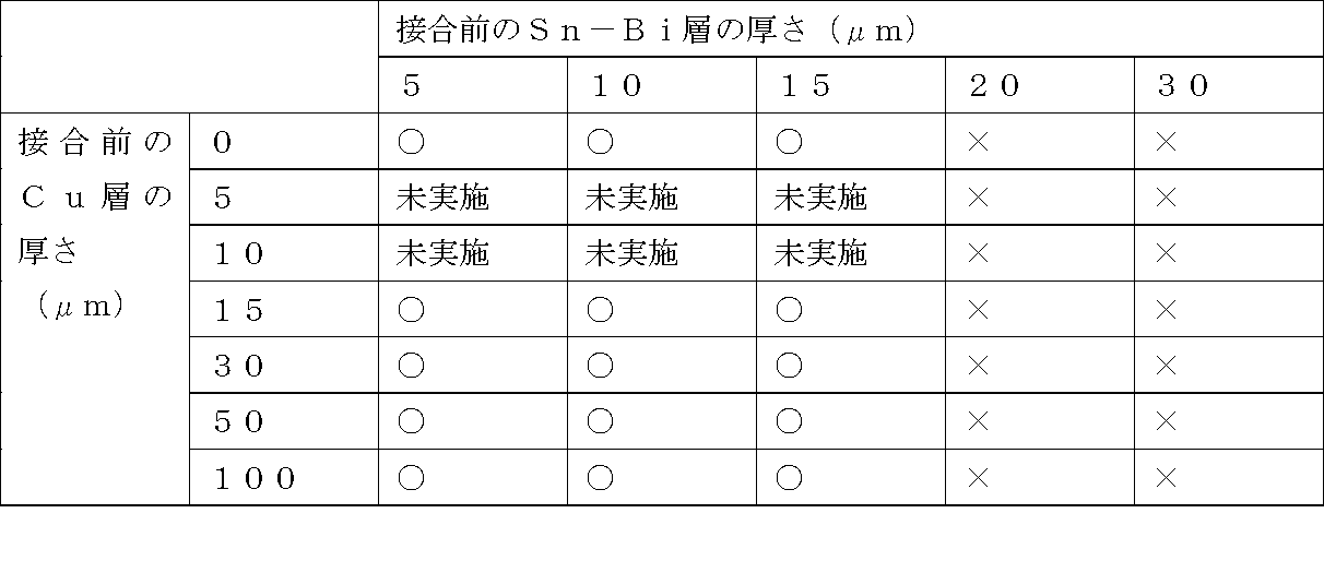
次に、接合前の接合材料におけるCu層の厚みと接合後の接合部におけるCu層の厚みとの関係を検討した。これは、接合プロセスにおいて、接合材料において、SnとCuが拡散反応により金属間化合物化すると、残存するCu層が減少する為、実際に接合後に応力緩和に必要なCu層の厚みを明らかにするためである。
図10から、接合前の接合材料におけるCu層の厚み15μm、Sn-Bi層の厚み15μmの場合、接合後の接合部において残存するCu層の平均厚みは7.2μmであり、最小厚さtmin3.7μmである。このことから、少なくとも接合後に接合部のCu層の最小厚さtminが3.7μm以上あれば、接合プロセスにおける熱応力に対して半導体素子のクラック発生或いは半導体素子と接合部との剥離を防ぐことと、耐熱性とを両立させることができると考えられる。
次に、半導体素子の電極との接合面の面積を変化させ、接合プロセスにおける異なる熱応力に対して、半導体素子のクラック発生或いは半導体素子と接合部との剥離の有無を検討した。接合前の接合材料のCu層の厚さ及び接合後の接合部のCu層の厚さと、半導体素子の電極との接合面の面積とに対する半導体素子のクラック発生或いは半導体素子と接合部との剥離の有無の結果を表3に示す。

実施の形態3では、図8(a)に示すように、半導体素子102の電極205としてAg層205を設け、基板101の電極103としてCu層103を設けた場合に、第1のSn-Bi層201、Cu層200、第2のSn-Bi層204が順に配置された接合材料223を用いて接合している。この場合、接合後には、図9(c)に示すように、半導体素子102の電極205と、電極103との間を接合する接合部232は、CuSn系の金属間化合物を含む第1の金属間化合物層227cと、Bi層229と、CuSn系の第2の金属間化合物層227dと、Cu層200と、CuSn系の第3の金属間化合物層228cと、Bi層230と、CuSn系の金属間化合物を主相とし、AgSn系の金属間化合物が第2相として含まれる第4の金属間化合物層228dと、を備える。
まず、半導体素子の電極は、Ag層に限られず、例えば、Cu層、Sn層、Ni層、Au層、あるいは、これらの中から選択された複数の層を配置したものであってもよい。
また、基板の電極は、Cu層に限られず、例えば、Ag層、Sn層、Ni層、Au層、あるいは、これらの中から選択された複数の層を配置したものであってもよい。
さらに、Cu層の厚さは、隣接するSn-Bi層の厚さ以上であることが必要となる。これは、接合後の接合部において、層状のCu層とBi層を残存させるために必要な条件である。

また、接合材料を構成する各層の厚みの割合に関しては、上記実施例の検討と同様、接合後の半導体素子との接合面の面積に応じて、接合構造体の歩留まり、製品の歩留まりに応じて決定すればよい。
101 基板
102 半導体素子
103 電極
104 接合部
106 接合構造体
200 Cu層
201 Sn-Bi層
202 Sn層
203、213、223 接合材料
204 第2のSn-Bi層
205 電極、Ag層
206 Sn層
207a、207b 金属間化合物層
207c 第1の金属間化合物層
207d 第2の金属間化合物層
208a、208b 金属間化合物層
208c 第3の金属間化合物層
209、209a、209b Bi層
212、212a、212b 接合部
217a、217b 金属間化合物層
217c 第1の金属間化合物層
218a、218b 金属間化合物層
218c 第2の金属間化合物層
218d 第3の金属間化合物層
220a、220b、220 Bi層
222 接合部
227a、227b 金属間化合物層
227c 第1の金属間化合物層
227d 第2の金属間化合物層
228a、228b 金属間化合物層
228c 第3の金属間化合物層
228d 第4の金属間化合物層
229a、229b、230a、230b、229、230 Bi層
232、232a、232b 接合部
602 パワー半導体素子
603 電極
604 接合部
Claims (9)
- 基板の電極と、
半導体素子の電極と、
前記基板の電極と前記半導体素子の電極との間を接合する接合部と、
を備え、
前記接合部は、
CuSn系の金属間化合物を含む、第1の金属間化合物層と、
Bi層と、
CuSn系の金属間化合物を含む、第2の金属間化合物層と、
Cu層と、
CuSn系の金属間化合物を含む、第3の金属間化合物層と、
が前記基板の電極から前記半導体素子の電極に向かって順に配置されている、接合構造体。 - 前記接合部は、前記第3の金属間化合物層と前記半導体素子の電極との間に、さらに、
Bi層と、
CuSn系の金属間化合物を含む、第4の金属間化合物層と、
が順に配置されている、請求項1に記載の接合構造体。 - 前記CuSn系の金属間化合物は、Cu6Sn5、及び、Cu3Snの少なくとも一つの金属間化合物を含む、請求項1または2に記載の接合構造体。
- 前記Cu層の厚さが6.2μm以上である、請求項1から3のいずれか一項に記載の接合構造体。
- 前記接合部と前記半導体素子の電極との接合面の面積は、5mm2以上であって100mm2以下である、請求項4に記載の接合構造体。
- 前記第1の金属間化合物層は、CuSn系の金属間化合物を有し、AgSn系金属間化合物を含む、請求項1または2に記載の接合構造体。
- 前記第4の金属間化合物層は、CuSn系の金属間化合物を有し、AgSn系金属間化合物を含む、請求項2に記載の接合構造体。
- 基板の電極と半導体素子の電極との間に挿入する接合材料であって、
前記接合材料は、
Sn層と、
Cu層と、
Sn-Bi層と、
が順に配置され、
前記Cu層の厚さは、隣接する前記Sn層及び前記Sn-Bi層の厚さ以上である、接合材料。 - 基板の電極と半導体素子の電極との間に挿入する接合材料であって、
前記接合材料は、
第1のSn-Bi層と、
Cu層と、
第2のSn-Bi層と、
が順に配置され、
前記Cu層の厚さは、隣接する前記第1及び第2のSn-Bi層のそれぞれの厚さ以上である、接合材料。
Priority Applications (4)
| Application Number | Priority Date | Filing Date | Title |
|---|---|---|---|
| EP12862148.9A EP2800129A4 (en) | 2011-12-27 | 2012-12-26 | CONNECTION STRUCTURE |
| US14/114,337 US8957521B2 (en) | 2011-12-27 | 2012-12-26 | Mounted structure |
| CN201280015910.6A CN103493190A (zh) | 2011-12-27 | 2012-12-26 | 接合结构体 |
| JP2013551248A JP5608824B2 (ja) | 2011-12-27 | 2012-12-26 | 接合構造体 |
Applications Claiming Priority (2)
| Application Number | Priority Date | Filing Date | Title |
|---|---|---|---|
| JP2011-284893 | 2011-12-27 | ||
| JP2011284893 | 2011-12-27 |
Publications (1)
| Publication Number | Publication Date |
|---|---|
| WO2013099243A1 true WO2013099243A1 (ja) | 2013-07-04 |
Family
ID=48696776
Family Applications (1)
| Application Number | Title | Priority Date | Filing Date |
|---|---|---|---|
| PCT/JP2012/008324 WO2013099243A1 (ja) | 2011-12-27 | 2012-12-26 | 接合構造体 |
Country Status (5)
| Country | Link |
|---|---|
| US (1) | US8957521B2 (ja) |
| EP (1) | EP2800129A4 (ja) |
| JP (1) | JP5608824B2 (ja) |
| CN (1) | CN103493190A (ja) |
| WO (1) | WO2013099243A1 (ja) |
Families Citing this family (8)
| Publication number | Priority date | Publication date | Assignee | Title |
|---|---|---|---|---|
| DE102012201935A1 (de) * | 2012-02-09 | 2013-08-14 | Robert Bosch Gmbh | Verbindungsanordnung eines elektrischen und/oder elektronischen Bauelements |
| US9024205B2 (en) * | 2012-12-03 | 2015-05-05 | Invensas Corporation | Advanced device assembly structures and methods |
| US9355980B2 (en) * | 2013-09-03 | 2016-05-31 | Taiwan Semiconductor Manufacturing Company, Ltd. | Three-dimensional chip stack and method of forming the same |
| JP6380539B2 (ja) * | 2014-08-22 | 2018-08-29 | 株式会社豊田自動織機 | 接合構造、接合材、及び接合方法 |
| US10115716B2 (en) * | 2015-07-18 | 2018-10-30 | Semiconductor Components Industries, Llc | Die bonding to a board |
| JP6042577B1 (ja) * | 2016-07-05 | 2016-12-14 | 有限会社 ナプラ | 多層プリフォームシート |
| JP6621068B2 (ja) * | 2016-12-08 | 2019-12-18 | パナソニックIpマネジメント株式会社 | 実装構造体 |
| WO2021059485A1 (ja) * | 2019-09-27 | 2021-04-01 | 三菱電機株式会社 | 光半導体装置およびその製造方法 |
Citations (4)
| Publication number | Priority date | Publication date | Assignee | Title |
|---|---|---|---|---|
| JP2000054189A (ja) * | 1998-08-10 | 2000-02-22 | Furukawa Electric Co Ltd:The | Sn−Bi系はんだを接合して用いられる電気・電子部品用材料、それを用いた電気・電子部品、電気・電子部品実装基板、それを用いたはんだ接合または実装方法 |
| JP2001230351A (ja) * | 2000-02-14 | 2001-08-24 | Shibafu Engineering Corp | 電子モジュール用接合材料、モジュール型半導体装置及びその製造方法 |
| WO2005020315A1 (ja) * | 2003-08-26 | 2005-03-03 | Tokuyama Corporation | 素子接合用基板、素子接合基板及びその製造方法 |
| JP2009290007A (ja) | 2008-05-29 | 2009-12-10 | Toshiba Corp | 接合体、半導体装置および接合体の製造方法 |
Family Cites Families (13)
| Publication number | Priority date | Publication date | Assignee | Title |
|---|---|---|---|---|
| JP2003198117A (ja) * | 2001-12-28 | 2003-07-11 | Matsushita Electric Ind Co Ltd | はんだ付け方法および接合構造体 |
| US8169684B2 (en) * | 2002-09-30 | 2012-05-01 | Gentex Corporation | Vehicular rearview mirror elements and assemblies incorporating these elements |
| TW200423344A (en) * | 2002-12-31 | 2004-11-01 | Texas Instruments Inc | Composite metal column for mounting semiconductor device |
| US7247030B2 (en) * | 2004-04-05 | 2007-07-24 | Tyco Electronics Corporation | Bonded three dimensional laminate structure |
| JP4145287B2 (ja) * | 2004-06-17 | 2008-09-03 | 株式会社ルネサステクノロジ | 半導体装置および半導体装置の製造方法 |
| JP4344707B2 (ja) * | 2005-02-24 | 2009-10-14 | 株式会社ルネサステクノロジ | 半導体装置およびその製造方法 |
| JP4742844B2 (ja) * | 2005-12-15 | 2011-08-10 | ルネサスエレクトロニクス株式会社 | 半導体装置の製造方法 |
| JP2007288001A (ja) * | 2006-04-18 | 2007-11-01 | Toshiba Corp | 半導体装置及びその製造方法、並びに半導体装置用部材 |
| WO2011049128A1 (ja) * | 2009-10-20 | 2011-04-28 | ローム株式会社 | 半導体装置および半導体装置の製造方法 |
| KR100976812B1 (ko) * | 2010-02-08 | 2010-08-20 | 옵토팩 주식회사 | 전자 소자 패키지 및 그 제조 방법 |
| US8348139B2 (en) * | 2010-03-09 | 2013-01-08 | Indium Corporation | Composite solder alloy preform |
| KR100976813B1 (ko) * | 2010-04-23 | 2010-08-20 | 옵토팩 주식회사 | 전자 소자 패키지 및 그 제조 방법 |
| JP2012174332A (ja) * | 2011-02-17 | 2012-09-10 | Fujitsu Ltd | 導電性接合材料、導体の接合方法、及び半導体装置の製造方法 |
-
2012
- 2012-12-26 WO PCT/JP2012/008324 patent/WO2013099243A1/ja active Application Filing
- 2012-12-26 EP EP12862148.9A patent/EP2800129A4/en not_active Withdrawn
- 2012-12-26 US US14/114,337 patent/US8957521B2/en not_active Expired - Fee Related
- 2012-12-26 CN CN201280015910.6A patent/CN103493190A/zh active Pending
- 2012-12-26 JP JP2013551248A patent/JP5608824B2/ja not_active Expired - Fee Related
Patent Citations (4)
| Publication number | Priority date | Publication date | Assignee | Title |
|---|---|---|---|---|
| JP2000054189A (ja) * | 1998-08-10 | 2000-02-22 | Furukawa Electric Co Ltd:The | Sn−Bi系はんだを接合して用いられる電気・電子部品用材料、それを用いた電気・電子部品、電気・電子部品実装基板、それを用いたはんだ接合または実装方法 |
| JP2001230351A (ja) * | 2000-02-14 | 2001-08-24 | Shibafu Engineering Corp | 電子モジュール用接合材料、モジュール型半導体装置及びその製造方法 |
| WO2005020315A1 (ja) * | 2003-08-26 | 2005-03-03 | Tokuyama Corporation | 素子接合用基板、素子接合基板及びその製造方法 |
| JP2009290007A (ja) | 2008-05-29 | 2009-12-10 | Toshiba Corp | 接合体、半導体装置および接合体の製造方法 |
Non-Patent Citations (1)
| Title |
|---|
| See also references of EP2800129A4 |
Also Published As
| Publication number | Publication date |
|---|---|
| US8957521B2 (en) | 2015-02-17 |
| CN103493190A (zh) | 2014-01-01 |
| EP2800129A1 (en) | 2014-11-05 |
| US20140048942A1 (en) | 2014-02-20 |
| JPWO2013099243A1 (ja) | 2015-04-30 |
| EP2800129A4 (en) | 2015-07-08 |
| JP5608824B2 (ja) | 2014-10-15 |
Similar Documents
| Publication | Publication Date | Title |
|---|---|---|
| JP5608824B2 (ja) | 接合構造体 | |
| CN102917835B (zh) | 接合材料、接合材料的制造方法以及接合结构的制造方法 | |
| JP2010179336A (ja) | 接合体、半導体モジュール、及び接合体の製造方法 | |
| JP5546067B2 (ja) | 半導体接合構造体および半導体接合構造体の製造方法 | |
| JP5523680B2 (ja) | 接合体、半導体装置および接合体の製造方法 | |
| WO2017217145A1 (ja) | はんだ接合部 | |
| TW200829361A (en) | Connecting material, method for manufacturing connecting material, and semiconductor device | |
| US20130043594A1 (en) | Method for manufacturing semiconductor device and semiconductor device | |
| JP5708961B2 (ja) | 半導体装置の製造方法 | |
| TW200903575A (en) | Substrate bonding method and semiconductor device | |
| KR102133765B1 (ko) | 납땜 이음 및 납땜 이음의 형성 방법 | |
| JP2009129983A (ja) | 接合体及びその製造方法、並びにパワー半導体モジュール及びその製造方法 | |
| WO2021085451A1 (ja) | 銅/セラミックス接合体、絶縁回路基板、及び、銅/セラミックス接合体の製造方法、絶縁回路基板の製造方法 | |
| ES2928498T3 (es) | Método de fase líquida transitoria de plata-indio de unión de dispositivo semiconductor y soporte de dispersión de calor y estructura semiconductora que tiene una junta de unión de fase líquida transitoria de plata-indio | |
| JP2010073908A (ja) | 半導体装置およびその製造方法 | |
| JP4917375B2 (ja) | パワー半導体モジュールの製造方法 | |
| TW201308543A (zh) | 接合構造體 | |
| WO2010125800A1 (ja) | 接合構造体と接合構造体の接合方法 | |
| JP6156693B2 (ja) | 半導体装置の製造方法 | |
| JP2020155761A (ja) | 接合構造及び液相拡散接合方法 | |
| US11817417B2 (en) | Semiconductor device and method for fabricating a semiconductor device | |
| JP2013035046A (ja) | 金属膜とリードのはんだ接合構体およびその熱処理方法 | |
| JP6493161B2 (ja) | 半導体装置の製造方法 | |
| JP2011009331A (ja) | 層を有した半導体素子およびその半導体素子を用いた接合構造体 | |
| CN104465578A (zh) | 半导体装置及半导体模块 |
Legal Events
| Date | Code | Title | Description |
|---|---|---|---|
| 121 | Ep: the epo has been informed by wipo that ep was designated in this application |
Ref document number: 12862148 Country of ref document: EP Kind code of ref document: A1 |
|
| ENP | Entry into the national phase |
Ref document number: 2013551248 Country of ref document: JP Kind code of ref document: A |
|
| REEP | Request for entry into the european phase |
Ref document number: 2012862148 Country of ref document: EP |
|
| WWE | Wipo information: entry into national phase |
Ref document number: 2012862148 Country of ref document: EP |
|
| WWE | Wipo information: entry into national phase |
Ref document number: 14114337 Country of ref document: US |
|
| NENP | Non-entry into the national phase |
Ref country code: DE |