WO2013027760A1 - 弾性波装置および電子部品 - Google Patents
弾性波装置および電子部品 Download PDFInfo
- Publication number
- WO2013027760A1 WO2013027760A1 PCT/JP2012/071181 JP2012071181W WO2013027760A1 WO 2013027760 A1 WO2013027760 A1 WO 2013027760A1 JP 2012071181 W JP2012071181 W JP 2012071181W WO 2013027760 A1 WO2013027760 A1 WO 2013027760A1
- Authority
- WO
- WIPO (PCT)
- Prior art keywords
- element substrate
- frame portion
- wall
- frame
- main surface
- Prior art date
- Legal status (The legal status is an assumption and is not a legal conclusion. Google has not performed a legal analysis and makes no representation as to the accuracy of the status listed.)
- Ceased
Links
Images


Classifications
-
- H—ELECTRICITY
- H03—ELECTRONIC CIRCUITRY
- H03H—IMPEDANCE NETWORKS, e.g. RESONANT CIRCUITS; RESONATORS
- H03H9/00—Networks comprising electromechanical or electro-acoustic elements; Electromechanical resonators
- H03H9/02—Details
- H03H9/05—Holders or supports
- H03H9/10—Mounting in enclosures
- H03H9/1064—Mounting in enclosures for surface acoustic wave [SAW] devices
- H03H9/1092—Mounting in enclosures for surface acoustic wave [SAW] devices the enclosure being defined by a cover cap mounted on an element forming part of the surface acoustic wave [SAW] device on the side of the IDT's
-
- H—ELECTRICITY
- H03—ELECTRONIC CIRCUITRY
- H03H—IMPEDANCE NETWORKS, e.g. RESONANT CIRCUITS; RESONATORS
- H03H9/00—Networks comprising electromechanical or electro-acoustic elements; Electromechanical resonators
- H03H9/02—Details
- H03H9/02535—Details of surface acoustic wave devices
- H03H9/02992—Details of bus bars, contact pads or other electrical connections for finger electrodes
-
- H—ELECTRICITY
- H03—ELECTRONIC CIRCUITRY
- H03H—IMPEDANCE NETWORKS, e.g. RESONANT CIRCUITS; RESONATORS
- H03H9/00—Networks comprising electromechanical or electro-acoustic elements; Electromechanical resonators
- H03H9/02—Details
- H03H9/05—Holders or supports
- H03H9/10—Mounting in enclosures
- H03H9/1007—Mounting in enclosures for bulk acoustic wave [BAW] devices
- H03H9/105—Mounting in enclosures for bulk acoustic wave [BAW] devices the enclosure being defined by a cover cap mounted on an element forming part of the BAW device
-
- H—ELECTRICITY
- H03—ELECTRONIC CIRCUITRY
- H03H—IMPEDANCE NETWORKS, e.g. RESONANT CIRCUITS; RESONATORS
- H03H9/00—Networks comprising electromechanical or electro-acoustic elements; Electromechanical resonators
- H03H9/15—Constructional features of resonators consisting of piezoelectric or electrostrictive material
- H03H9/17—Constructional features of resonators consisting of piezoelectric or electrostrictive material having a single resonator
- H03H9/171—Constructional features of resonators consisting of piezoelectric or electrostrictive material having a single resonator implemented with thin-film techniques, i.e. of the film bulk acoustic resonator [FBAR] type
-
- H—ELECTRICITY
- H10—SEMICONDUCTOR DEVICES; ELECTRIC SOLID-STATE DEVICES NOT OTHERWISE PROVIDED FOR
- H10N—ELECTRIC SOLID-STATE DEVICES NOT OTHERWISE PROVIDED FOR
- H10N30/00—Piezoelectric or electrostrictive devices
- H10N30/80—Constructional details
- H10N30/87—Electrodes or interconnections, e.g. leads or terminals
- H10N30/875—Further connection or lead arrangements, e.g. flexible wiring boards, terminal pins
-
- H—ELECTRICITY
- H10—SEMICONDUCTOR DEVICES; ELECTRIC SOLID-STATE DEVICES NOT OTHERWISE PROVIDED FOR
- H10N—ELECTRIC SOLID-STATE DEVICES NOT OTHERWISE PROVIDED FOR
- H10N30/00—Piezoelectric or electrostrictive devices
- H10N30/80—Constructional details
- H10N30/88—Mounts; Supports; Enclosures; Casings
- H10N30/883—Additional insulation means preventing electrical, physical or chemical damage, e.g. protective coatings
Definitions
- the present invention relates to an acoustic wave device such as a surface acoustic wave (SAW) device or a piezoelectric thin film resonator (FBAR), and an electronic component using the same.
- SAW surface acoustic wave
- FBAR piezoelectric thin film resonator
- WLP Wafer Level Package
- This WLP type acoustic wave device has a piezoelectric substrate, an excitation electrode provided on the piezoelectric substrate, and a cover for sealing the excitation electrode (see, for example, Patent Document 1).
- the cover includes an annular frame portion surrounding the excitation electrode disposed on the upper surface of the piezoelectric substrate and a lid portion disposed on the upper surface of the frame portion so as to close the opening of the frame portion. In this way, the opening of the frame portion is closed by the lid portion, so that a vibration space that is an area surrounded by the inner wall of the frame portion and the lower surface of the lid portion is secured on the excitation electrode.
- the frame part and the cover part constituting the cover are often formed of the same material, the frame part and the cover part are slightly formed between the frame part and the cover part when the frame part and the cover part are formed through different processes. Gaps may be formed.
- the atmosphere in the vibration space is changed by connecting the outside of the cover and the vibration space through the gap. For example, if moisture in the outside air enters the vibration space through the gap, it causes corrosion of the excitation electrode. If the excitation electrode corrodes, the electrical characteristics of the acoustic wave device will deteriorate.
- an elastic wave device that can maintain the hermeticity of the vibration space for a long time even when the cover is composed of a frame portion and a lid portion.
- An elastic wave device includes an element substrate, an excitation electrode positioned on the main surface of the element substrate, a frame portion positioned on the main surface of the element substrate so as to surround the excitation electrode, and the A cover that includes a lid portion that overlaps the frame portion and closes the frame portion, and has a hanging portion that extends from the upper side of the inner wall of the frame portion or the upper side of the outer wall and covers at least a part of the inner wall or the outer wall. It is equipped with.
- An acoustic wave device includes an element substrate, an excitation electrode positioned on the principal surface of the element substrate, a frame portion positioned on the principal surface of the element substrate so as to surround the excitation electrode, and A cover including a lid portion that overlaps the frame portion and closes the frame portion, the frame portion has a frame-side uneven portion on the upper surface, and the lid portion has a lid-side uneven portion on the lower surface. And this cover part side uneven
- an electronic component as one aspect of the present invention includes a mounting substrate and the elastic wave device mounted via a conductive bonding material in a state where the main surface of the element substrate faces the main surface of the mounting substrate And a mold resin that covers the acoustic wave device.
- the elastic wave device having the above-described configuration is provided with a hanging part that covers at least a part of the inner wall from the upper side of the inner wall of the frame part. Since the infiltration path of moisture and the like from the outside air to the vibration space becomes long, the airtightness of the vibration space can be maintained in a normal state for a long time.
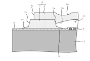
- FIG. 2 is a sectional view taken along line II-II in FIG.
- FIG. 3 is an enlarged view of a region indicated by III in FIG. 2. It is sectional drawing of the electronic component which concerns on embodiment of this invention.
- (A) to (d) are cross-sectional views for explaining a method of manufacturing the electronic component of FIG. (A) to (c) is a cross-sectional view showing a continuation of FIG. It is an expanded sectional view which shows the modification of the SAW apparatus shown in FIG.
- FIGS. 9A to 9C are cross-sectional views illustrating a method for manufacturing a SAW device according to the fourth embodiment.
- FIGS. 9A to 9C are cross-sectional views for explaining a method of manufacturing a SAW device according to the fourth embodiment, and show a process following FIG. It is sectional drawing for demonstrating the reason a microprotrusion is formed in the internal peripheral surface of a 2nd through-hole. It is sectional drawing which shows the modification of the SAW apparatus which concerns on 4th Embodiment.
- FIG. 16 is a partial cross-sectional view taken along line XVI-XVI in FIG. 15. It is sectional drawing of the reference
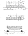
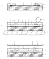
- FIG. 1A is a plan view of the SAW device 1 according to the first embodiment of the present invention
- FIG. 1B is a plan view of the SAW device 1 with the lid 4 removed.
- FIG. 2 is a cross-sectional view taken along the line II-II in FIG.
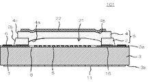
- the SAW device 1 includes an element substrate 3, an excitation electrode 5 provided on the first main surface 3a of the element substrate 3, a pad 7 provided on the first main surface 3a and connected to the excitation electrode 5,
- the cover 9 covers the excitation electrode 5 and exposes the pad 7, and the back surface portion 11 is provided on the second main surface 3 b of the element substrate 3.
- the SAW device 1 receives a signal through any of the plurality of pads 7.
- the input signal is filtered by the excitation electrode 5 or the like. Then, the SAW device 1 outputs the filtered signal via any of the plurality of pads 7.
- the specific configuration of each member is as follows.
- the element substrate 3 is constituted by a piezoelectric substrate.
- the element substrate 3 is composed of a single crystal substrate having piezoelectricity, such as a lithium tantalate single crystal or a lithium niobate single crystal.
- the element substrate 3 is formed in a rectangular parallelepiped shape, for example, and has a first main surface 3a and a second main surface 3b which are rectangular and parallel to each other and are flat.
- the size of the element substrate 3 may be set as appropriate.
- the thickness (Z direction) is 0.2 mm to 0.5 mm
- the length of one side (X direction or Y direction) is 0.5 mm. ⁇ 3 mm.
- the excitation electrode 5 is formed on the first main surface 3a.
- the excitation electrode 5 is a so-called IDT (InterDigital Transducer), and has a pair of comb-like electrodes.
- Each comb-like electrode has a bus bar extending in the propagation direction of the surface acoustic wave on the element substrate 3 and a plurality of electrode fingers extending from the bus bar in a direction orthogonal to the propagation direction of the surface acoustic wave.
- the two comb-like electrodes are provided so that their electrode fingers mesh with each other.
- FIG. 1 and the like are schematic diagrams, a pair of comb-like electrodes having several electrode fingers is shown, but in practice, a plurality of pairs of combs having a larger number of electrode fingers are shown. Toothed electrodes may be provided. Further, a ladder-type SAW filter in which a plurality of excitation electrodes 5 are connected by a system such as series connection or parallel connection may be configured, or a plurality of excitation electrodes 5 are arranged in the propagation direction of a surface acoustic wave. A mode SAW resonator filter may be configured.
- the pad 7 is formed on the first main surface 3a.
- the planar shape of the pad 7 may be set as appropriate.
- the planar shape is a circle.
- the number and arrangement position of the pads 7 are appropriately set according to the configuration of the filter constituted by the excitation electrodes 5.
- the SAW device 1 the case where the six pads 7 are arranged along the outer periphery of the 1st main surface 3a is illustrated.
- Excitation electrode 5 and pad 7 are connected by wiring 15.
- the wiring 15 is formed on the first main surface 3 a and connects the bus bar of the excitation electrode 5 and the pad 7.
- the wiring 15 may be three-dimensionally crossed with not only a portion formed on the first main surface 3a but also two wirings 15 through which different signals flow with an insulator interposed therebetween.
- the excitation electrode 5, the pad 7 and the wiring 15 are made of the same conductive material, for example.
- the conductive material is, for example, an Al alloy such as Al or an Al—Cu alloy.
- the excitation electrode 5, the pad 7 and the wiring 15 are formed with the same thickness, for example, and these thicknesses are, for example, 100 to 500 nm.
- the wires 15 on the first main surface 3a side are formed of, for example, an Al—Cu alloy, and the wires 15 disposed thereon via an insulator are, for example, sequentially from the bottom. It is formed by wiring having a multilayer structure of Cr / Ni / Au or Cr / Al.
- the cover 9 made of resin is not laminated on the three-dimensional wiring. It is good to do so. Thereby, peeling of the cover 9 can be suppressed.
- the cover 9 may be laminated on the three-dimensional wiring.
- connection reinforcing layer 6 for the purpose of improving the connectivity with the conductive bonding material in addition to the same material and the same thickness as the excitation electrode 5.
- the connection reinforcing layer 6 includes, for example, a nickel layer superimposed on the pad 7 and a gold layer superimposed on the nickel layer.
- the cover 9 has, for example, a protruding portion 9a that protrudes between adjacent pads 7, and the planar shape excluding the protruding portion 9a is roughly rectangular.
- the cover 9 can be regarded as a shape that is cut out so that the pad 7 is exposed from a rectangle having a size that covers the pad 7.
- the cover 9 is provided on the first main surface 3 a, the frame portion 2 surrounding the excitation electrode 5 in a plan view of the first main surface 3 a, and the lid portion 4 that overlaps the frame portion 2 and closes the opening of the frame portion 2. And have.
- a vibration space 21 is formed by the space surrounded by the first main surface 3a, the frame portion 2 and the lid portion 4 so as not to hinder the vibration of the SAW excited by the excitation electrode 5.
- the planar shape of the vibration space 21 may be set as appropriate, but the SAW device 1 is generally rectangular.
- the cover 9 may be regarded as having a shape in which a concave portion constituting the vibration space 21 is formed on the lower surface side.
- the frame part 2 is configured by forming one or more openings to be the vibration space 21 in a layer having a substantially constant thickness.
- the thickness of the frame portion 2 (height of the vibration space 21) is, for example, several ⁇ m to 30 ⁇ m.
- the lid portion 4 is constituted by a layer having a substantially constant thickness. The thickness of the lid 4 is, for example, several ⁇ m to 30 ⁇ m.
- the planar shape of the lid portion 4 is, for example, substantially the same as the planar shape of the frame portion 2, and the lid portion 4 is formed to be slightly smaller than the frame portion 2.
- the frame portion 2 is sized so that a portion along the outer periphery of the frame portion 2 slightly protrudes from the lid portion 4 when viewed in plan.
- the frame part 2 and the lid part 4 may be formed of the same material, or may be formed of different materials.
- the boundary between the frame 2 and the lid 4 is clearly shown as a boundary line.
- the frame 2 and the lid 4 are integrally formed of the same material. May be.
- the cover 9 (the frame portion 2 and the lid portion 4) is made of a photosensitive resin.
- the photosensitive resin is, for example, a urethane acrylate-based, polyester acrylate-based, or epoxy acrylate-based resin that is cured by radical polymerization of an acryl group or a methacryl group.
- a polyimide resin or the like can also be used.
- the back surface portion 11 has, for example, a back electrode that covers substantially the entire second main surface 3b of the element substrate 3 and an insulating protective layer that covers the back electrode.
- the back surface electrode discharges the charge charged on the surface of the element substrate 3 due to a temperature change or the like. Damage to the element substrate 3 is suppressed by the protective layer.
- illustration and description of the back surface portion 11 may be omitted.
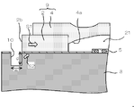
- FIG. 3 is an enlarged view of region III in FIG.
- a protective layer 8 is disposed on the first main surface 3 a of the element substrate 3, and a cover 9 is disposed on the protective layer 8.
- the protective layer 8 covers the excitation electrode 5 and contributes to prevention of oxidation of the excitation electrode 5.
- the protective layer 8 is made of, for example, silicon oxide (such as SiO 2 ), aluminum oxide, zinc oxide, titanium oxide, silicon nitride, or silicon.
- the thickness of the protective layer 8 is, for example, about 1/10 (10 to 30 nm) of the thickness of the excitation electrode 5 or 200 nm to 1500 nm, which is thicker than the excitation electrode 5.
- connection reinforcing layer 6 is exposed from the protective layer 8.
- the opening for exposing the connection reinforcing layer 6 of the protective layer 8 has the same shape and area as the connection reinforcing layer 6, but the opening is larger than the connection reinforcing layer 6. Alternatively, it may be small (a portion around the opening of the protective layer 8 may cover the outer peripheral portion of the connection reinforcing layer 6).
- the SAW device 1 has a lid portion 4 having a hanging portion 4a.
- the hanging part 4a is a part of the lid part 4 that is continuous from the upper side of the inner wall 2a of the frame part 2 and covers at least a part of the inner wall 2a.
- the hanging part 4 a covers almost the upper half of the inner wall 2 a of the frame part 2.
- the hanging portion 4 a is in contact with the inner wall of the frame portion 2 as indicated by a white arrow in the intrusion route. Since it becomes longer by that amount, it becomes difficult for moisture to enter the vibration space 21. Therefore, corrosion of the excitation electrode 5 and the like in the vibration space can be suppressed, and the electrical characteristics of the SAW device 1 can be stabilized over a long period of time.
- the hanging part 4a is formed in, for example, an annular shape when viewed in plan. That is, the inner wall 2 a is covered so as to go around along the inner wall 2 a of the frame portion 2. As a result, it is possible to further enhance the effect of preventing moisture from entering between the lid portion 4 and the frame portion 2.
- the hanging part 4a can be formed, for example, by adjusting conditions such as temperature when the lid part 4 is attached to the frame part 2. For example, heating may be performed at a somewhat high temperature in order to attach the resin lid portion 4 and the resin frame portion 2 to each other, but the temperature at that time is slightly higher than usual, and the temperature holding time is longer than usual. By adjusting the temperature and holding time, such as slightly longer, a part of the resin lid part 4 hangs down along the inner wall 2a of the frame part 2, and the part becomes solid, thereby forming a sag part 4a. it can. As the hanging part 4a is formed, a minute recess 4b may be formed in a region directly above the hanging part 4a in the upper surface of the lid part 4.
- the outer wall 2b of the frame portion 2 is inclined so as to go outward as it goes to the first main surface 3a of the element substrate 3.
- the angle ⁇ of the outer wall 2b of the frame part 2 with respect to the first main surface 3a is, for example, about 80 °.
- the lower end of the outer wall 2b is separated from the connection reinforcing layer 6 (or the pad 7 when there is no connection reinforcing layer 6). The distance is, for example, 40 ⁇ m to 65 ⁇ m.
- the side wall 4c of the lid part 4 may or may not be inclined so as to go outward as it goes to the first main surface 3a of the element substrate 3.
- the angle ⁇ with respect to the main surface 3a of the outer wall 4b of the lid 4 may be the same as, for example, the angle ⁇ , may be increased, or may be decreased.
- the side wall 4 c of the lid part 4 is located slightly inside the outer wall 2 b of the frame part 2. In other words, the lid 4 is made slightly smaller than the frame 2 when viewed in plan.
- the side wall 4 c of the lid part 4 is located several ⁇ m to several tens of ⁇ m inside the outer wall 2 b of the frame part 2.
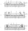
- FIG. 4 is a cross-sectional view showing a part of the electronic component 51 on which the SAW device 1 is mounted.
- the electronic component 51 includes a mounting substrate 53, a pad 55 provided on the mounting surface 53 a of the mounting substrate 53, a conductive bonding material 57 disposed on the pad 55, and a mounting surface via the conductive bonding material 57.
- the SAW device 1 mounted on 53a and a mold resin 59 for sealing the SAW device 1 are provided.
- the electronic component 51 includes, for example, an IC or the like mounted on the mounting substrate 53 and sealed together with the SAW device 1 by a mold resin 59 to form a module.
- the mounting substrate 53 is configured by, for example, a printed wiring board.
- the printed wiring board may be a rigid board or a flexible board.
- the printed wiring board may be a single-layer board, a two-layer board, or a multilayer board having two or more layers.
- the base material, insulating material, and conductive material of the printed wiring board may be selected from appropriate materials.
- the conductive bonding material 57 is in contact with both the pad 7 of the SAW device 1 and the pad 55 of the mounting substrate 53.
- the conductive bonding material 57 is formed of a metal that is melted by heating and bonded to the pad 7.
- the conductive bonding material 57 is made of, for example, solder.
- the solder may be a solder using lead such as Pb—Sn alloy solder, or lead-free solder such as Au—Sn alloy solder, Au—Ge alloy solder, Sn—Ag alloy solder, Sn—Cu alloy solder, etc. It may be.
- the mold resin 59 is mainly composed of, for example, an epoxy resin, a curing material, and a filler.
- the mold resin 59 not only covers the SAW device 1 from the back surface portion 11 side and the side, but also fills the space between the SAW device 1 and the mounting substrate 53. Specifically, the mold resin 59 is also filled between the upper surface of the cover 9 and the mounting surface 53 a of the mounting substrate 53 and around the conductive bonding material 57.
- the conductive bonding material 57 has a shape in which an approximately spherical shape such as a conductor bump is crushed by the pad 7 and the pad 55. That is, the conductive bonding material 57 has two planes in contact with the pad 7 and the pad 55 and an outer peripheral surface connecting the two planes.
- the two planes and the outer peripheral surface are circular in a plan view, and the outer peripheral surface is a side surface. When viewed, the center side has a curved shape protruding outward.
- the area of the plane in contact with the pad 7 and the pad 55 of the conductive bonding material 57 is preferably equal to or less than the area of the pad 7 and the pad 55.
- the side wall 2b of the frame portion 2 and the side wall 4b of the lid portion 4 are not in contact with the conductive bonding material 57 over the entirety. Therefore, a gap between the outer wall of the cover 9 (the frame portion 2 and the lid portion 4) and the conductive bonding material 57 is formed from the upper surface to the lower surface of the cover 9, and the gap is filled with the mold resin 59.
- the side wall 2b of the frame portion 2 and the side wall 4b of the lid portion 4 are not in contact with the conductive bonding material 57 over the whole, and the mold resin is not between the side walls and the conductive bonding material 57. Since it is filled, the conductive bonding material 57 is not easily affected by the shape of the outer wall of the cover 9. As a result, for example, the corners between the outer wall of the cover 9 and the upper surface of the cover are prevented from forming a shape that is likely to cause stress concentration in the conductive bonding material 57, and cracks in the conductive bonding material 57 are generated. Is suppressed. These effects are particularly remarkable when the mold resin 59 is filled between the conductive bonding material 57 and the outer wall of the cover 9 from the upper surface to the lower surface of the cover 9 as in the embodiment. Become.
- the outer wall 2b of the frame portion 2 constituting the cover 9 is inclined so as to expand toward the main surface 3a of the element substrate 3, and the mold resin 59 is in contact with the inclined outer wall 2b. ing.
- the mold resin 59 can easily flow from the upper surface side to the lower surface side of the cover 9, and the formation of a cavity in the mold resin 59 is suppressed. If there is a cavity in the mold resin 59, when the heat is applied during reflow, the cavity expands, which may cause a mounting failure of the SAW device 1, but the formation of the cavity is suppressed. Occurrence of a bad mounting failure or the like is suppressed.
- the outer wall 4c of the lid part 4 is located on the inner side of the outer wall 2b of the frame part 2, the same effect as that obtained by the inclination of the outer wall 2b of the frame part 2 is expected. That is, the mold resin 59 easily flows from the upper surface side to the lower surface side of the cover 9 between the outer wall of the cover 9 and the conductive bonding material 57.
- FIG. 5 (a) to 6 (c) are cross-sectional views (corresponding to the line III-III in FIG. 1) for explaining a method for manufacturing the SAW device 1 and the electronic component 51.
- FIG. The manufacturing process proceeds in order from FIG. 5 (a) to FIG. 6 (c).
- FIGS. 5A to 6A corresponding to the method for manufacturing the SAW device 1 is realized in a so-called wafer process. That is, a thin film formation, a photolithography method, or the like is performed on the mother substrate that becomes the element substrate 3 by being divided, and then a large number of SAW devices 1 are formed in parallel by dicing.
- FIGS. 5A to 6A only a portion corresponding to one SAW device 1 is shown.
- a common code may be used before and after the change.
- the excitation electrode 5, the pad 7, and the wiring 15 are formed on the main surface 3 a of the element substrate 3.
- a metal layer is formed on the main surface 3a by a thin film forming method such as a sputtering method, a vapor deposition method, or a CVD (Chemical Vapor Deposition) method.
- the metal layer is patterned by a photolithography method using a reduction projection exposure machine (stepper) and an RIE (Reactive (Ion Etching) apparatus.
- Excitation electrode 5, wiring 15 and pad 7 are formed by patterning.
- the protective layer 8 is formed as shown in FIG. Specifically, first, a thin film to be the protective layer 8 is formed by an appropriate thin film forming method.
- the thin film forming method is, for example, a sputtering method or CVD.
- a part of the thin film is removed by RIE or the like so that the pad 7 is exposed. Thereby, the protective layer 8 is formed.
- a thin film made of a photosensitive resin, which becomes the frame portion 2 is formed.
- the thin film is formed, for example, by attaching a film.
- the film includes, for example, a base film 31 and a resin layer 17 that becomes the frame portion 2 attached to the base film 31. After the resin layer 17 is brought into close contact with the protective layer 8, the base film 31 is peeled off as indicated by the arrow y1.
- the thin film used as the frame part 2 may be formed by the thin film formation method similar to the protective layer 8, and may be formed by a spin coat method etc. in addition.
- the thin film to be the frame portion 2 is formed, as shown in FIG. 5D, a region along the outer periphery of the element substrate 3 on which the thin film on the excitation electrode 5 and the pad 7 are arranged by a photolithography method or the like.
- the thin film is removed.
- the thin film is also removed with a constant width on the dicing line. In this way, the frame portion 2 is formed.
- the process of peeling the base film 31 may be performed after the exposure process of photolithography.
- a thin film made of a photosensitive resin, which becomes the cover part 4 is formed.
- the thin film is formed, for example, by attaching a film.
- the film includes, for example, a base film 32 and a resin layer 18 that becomes the lid 4 attached to the base film 32. And the resin layer 18 and the frame part 2 are adhere
- Adhesion between the resin layer 18 and the frame portion 2 is performed, for example, by placing the element substrate 3 on a stage 29 heated to about 40 ° C. to 50 ° C., and rotating the roller 30 similarly heated to about 40 ° C. to 50 ° C. in that state.
- the softened resin layer 18 can be dripped along the inner wall 2a of the frame portion 2, and this drooping A part becomes the drooping part 4a.
- the shape of the hanging part 4a can be controlled to some extent by adjusting the temperature of the stage 29 and the roller 30, the holding time on the stage 29, the rotational speed of the roller, and the like.
- the stage 29 and the roller 30 are several times higher than the temperature during normal bonding.
- the temperature is raised from 42 ° C. to about 45 ° C., the drooping portion 4a covering the upper half of the inner wall 2a of the frame portion 2 can be formed.
- the base film 32 is peeled off, and the region along the outer periphery of the resin layer 18 to be the lid portion 4 is removed by a photolithography method or the like as shown in FIG. 6B, and the lid portion 4 having the hanging portion 4a is formed. It is formed. Further, the thin film is removed with a constant width on the dicing line.
- a vibration space 21 including a space surrounded by the protective layer 8, the frame portion 2, and the lid portion 4 is formed.
- the method of forming the vibration space 21 is not limited to this, for example, a sacrificial layer is formed in advance on a portion where the vibration space 21 is to be formed, and a resin serving as a cover is formed so as to cover the sacrificial layer, Finally, it may be formed by removing the sacrificial layer.
- the SAW device 1 When the lid portion 4 is formed, the SAW device 1 is cut out from the wafer and mounted on the mounting substrate 53 as shown in FIG. Prior to mounting the SAW device 1, the pad 55 and the conductive bonding material 57 are provided on the mounting surface 53 a of the mounting substrate 53. If the conductive bonding material 57 is a conductor bump before the SAW device 1 is bonded, for example, a spherical or hemispherical surface is obtained by utilizing the effect of surface tension by vapor deposition, plating, or printing. It is formed in a shape.
- the SAW device 1 is arranged with the upper surface of the cover 9 facing the mounting surface 53a.
- the conductive bonding material 57 contacts the pad 7 on the SAW device 1 side and supports the SAW device 1. Thereafter, the SAW device 1 and the mounting substrate 53 are temporarily heated by being passed through a reflow furnace or the like, and the conductive bonding material 57 and the pad 7 are fixed by melting and solidification of the conductive bonding material 57.
- the mold resin 59 is supplied around the SAW device 1 by, for example, a transfer molding method or a printing method.
- the mold resin 59 supplied to the periphery of the SAW device 1 flows between the upper surface of the cover 9 and the mounting surface 53a by the applied pressure, and further, between the side surface of the cover 9 and the conductive bonding material 57. Flows in.
- the electronic component 51 is manufactured as shown in FIG.
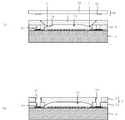
- FIG. 7 is an enlarged cross-sectional view showing a modified example of the SAW device 1 in the first embodiment. 7 corresponds to the part shown in FIG.
- the SAW device 1 according to this modification is different from the SAW device 1 shown in FIG. 1 in the shape of the hanging part 4a. Specifically, in the SAW device 1 according to the modification, the lower end of the hanging portion 4 a reaches the first main surface 3 a of the element substrate 3. Thus, since the contact area of the drooping part 4a and the inner wall 2a of the frame part 2 increases because the lower end of the drooping part 4a reaches the first main surface 3a, the adhesive strength between the lid part 4 and the frame part 2 is increased. At the same time, the moisture intrusion path between the lid portion 4 and the frame portion 2 becomes longer, so that moisture hardly enters the vibration space 21.
- FIG. 23 is an enlarged cross-sectional view showing another modified example of the SAW device 1 in the first embodiment, and is an enlarged cross-sectional view of a portion corresponding to the portion shown in FIG.
- the hanging part 4 a is also provided on the outer wall side of the frame part 2. That is, the SAW device 1 shown in FIG. 23A is continuous from the upper side of the inner wall 2a of the frame part 2 and from the upper side of the hanging part 4a covering a part of the inner wall 2a and the outer wall 2b of the frame part 2. It has a hanging part 4a that covers a part of the outer wall 2b.
- the contact area between the frame part 2 and the lid part 4 is further increased, so that the frame part 2 and the lid part 4 are peeled off.
- the suppression effect can be improved.
- the portion between the frame portion 2 and the lid portion 4 that can serve as a moisture intrusion path from the outside becomes longer, the effect of suppressing moisture intrusion into the vibration space 21 is also improved.
- the hanging part 4a is provided only on the outer wall side of the frame part 2, and is not provided on the inner wall side of the frame part 2.
- the frame part 2 and the lid part 4 are the same as the above-described SAW device 1 provided with the hanging part 4 a only on the inner wall side of the frame part 2.
- Can be prevented and moisture can be prevented from entering the vibration space 21.
- the hanging portion 4a is formed on the inner wall 2a side, the hanging portion 4a is likely to come into contact with the excitation electrode 5, so that FIG.
- the frame portion 2 and the lid portion 4 are peeled off and the vibration space is prevented while the contacting of the hanging portion 4a to the excitation electrode 5 is prevented. Intrusion of moisture into 21 can be suppressed.
- the position where the hanging part 4a is formed depends on, for example, the rotation speed or temperature of the roller 30 such that the rotation speed of the roller 30 shown in FIG. 6A is decreased at the position where the hanging part 4a is formed. It can be controlled by adjusting etc.
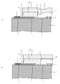
- FIG. 8 is a cross-sectional view corresponding to FIG. 2 showing the SAW device 101 of the second embodiment.
- the SAW device 101 has a reinforcing layer 22 disposed on the upper surface of the cover 9.
- the reinforcing layer 22 is for reinforcing the strength of the cover 9 (particularly the lid 4).
- the reinforcing layer 22 is formed over a relatively wide range of the cover 9.
- the reinforcing layer 22 is formed over substantially the entire upper surface of the cover 9. Therefore, the reinforcing layer 22 covers the entire vibration space 21 in a plan view, extends to the outside of the vibration space 21, and is supported by the frame portion 2 together with the lid portion 4.
- a minute recess 4b is formed in the upper surface of the cover 9 in a region immediately above the hanging portion 4a.
- the reinforcing layer 22 is formed on the inner surface of the minute recess 4b. It is formed in contact. Therefore, the contact area between the reinforcing layer 22 and the upper surface of the cover 9 is increased, and the peeling of the reinforcing layer 22 from the cover 9 can be suppressed.
- the reinforcing layer 22 is made of a material having a Young's modulus higher than that of the cover 9.
- the cover 9 is made of a resin having a Young's modulus of 0.5 to 1 GPa
- the reinforcing layer 22 is made of a metal having a Young's modulus of 100 to 250 GPa.
- the thickness of the reinforcing layer 22 is, for example, 1 to 50 ⁇ m.
- the reinforcing layer 22 has, for example, a base layer located directly on the upper surface of the cover 9 and a metal portion overlapping the base layer.
- the underlayer is formed of, for example, copper, titanium, or a laminate of these.
- the thickness of the underlayer is, for example, 300 nm to 1 ⁇ m when the underlayer is made of copper, and 10 nm to 100 nm when the underlayer is made of titanium.
- the metal part is made of, for example, copper.
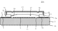
- FIG. 9 is a cross-sectional view corresponding to FIG. 2 showing the SAW device 201 of the third embodiment.
- the SAW device 201 has a sealing film 23 that covers the outer wall 2b of the frame portion 2 and the side wall 4c of the lid portion 4.
- the vibration space 21 such as moisture that can enter from between the frame part 2 and the lid part 4 is introduced into the vibration space 21.
- the invasion suppressing effect can be further enhanced.
- the sealing film 23 for example, an insulating material such as silicon oxide or silicon nitride, or a metal material such as copper can be used.
- the sealing film 23 is formed of a metal material, and is continuously formed not only from the outer wall 2 b of the frame portion 2 to the side wall 4 c of the lid portion 4 but also to the upper surface of the cover 9. As a result, the sealing film 23 can also be used as the reinforcing layer 22 of the SAW device 101 in the second embodiment.
- the side wall 4c of the lid part 4 is positioned on the inner side of the outer wall 2b of the frame part 2, there is a step in the portion between the outer wall 2b of the frame part 2 and the side wall 4c of the lid part 4, It becomes easy to form the sealing film 23 having a sufficient thickness on the portion between the outer wall 2 b of the frame portion 2 and the side wall 4 c of the lid portion 4.
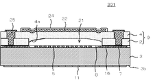
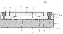
- FIG. 10 is a cross-sectional view corresponding to FIG. 2 showing the SAW device 301 of the fourth embodiment.
- the SAW device 301 has a terminal 25.
- the terminal 25 is located on the pad 7 in a state of being electrically connected to the pad 7. Further, the terminal 25 penetrates the cover 9 in the vertical direction, and the end portion not connected to the pad 7 is exposed from the upper surface of the cover 9.
- the terminal 7 is formed by plating using copper or the like, for example.
- the entire reinforcing layer 22 is covered with the insulating film 24. Therefore, when the SAW device 301 is mounted on the mounting substrate, the reinforcing layer 22 and the terminal 25 can be prevented from being short-circuited.
- a method for manufacturing the SAW device 301 will be described with reference to FIGS. 11 and 12.
- the steps up to the formation of the frame portion 2 are the same as the manufacturing steps of the SAW device 1, The description of the part is omitted, and the process of forming the frame part 2 will be described below.
- the first through hole 33 is formed on the pad 7 on which the columnar terminal 25 is formed.
- the resin layer 17 to be the frame portion 2 is patterned.
- the resin layer 18 to be the lid portion 4 is adhered to the frame portion 2 and the hanging portion 4 a is formed.
- This process is basically the same as the process of the SAW device 1 shown in FIG.
- a photosensitive negative resist is used as the resin layer 18.
- the mask 40 has a transparent substrate 38 and a light shielding portion 39 formed in a predetermined pattern on the lower surface of the transparent substrate 38.
- the light shielding portion 38 is disposed at a position corresponding to the position where the resin layer 18 is to be removed when the position of the mask 40 is set, and has a shape corresponding to the shape of the portion to be removed.
- a light shielding part 39 disposed immediately above the first through hole 33 and a light shielding part 39 disposed immediately above the region between the first through hole 33 and the vibration space 21 are provided. Yes.
- the reason why the light shielding part 39 is provided also in the portion directly above the region between the first through hole 33 and the vibration space 21 will be described in comparison with a case where such a light shielding part 39 is not provided.
- the minute protrusions 26 are formed on the inner peripheral surface of the second through hole 34 for arranging the upper portion of the terminal 25.
- FIG. 13A is a cross-sectional view showing a process of performing exposure using a mask 40 in which a light shielding portion 39 is not provided in a portion immediately above a region between the first through hole 33 and the vibration space 21.
- a part of the exposure light L is scattered at the lower end of the hanging part 4a, and a part of the scattered light is a part directly above the first through hole 33 in the resin layer 18. It is considered that Then, a portion that is not originally exposed is exposed, and it is assumed that when the development process is performed thereafter, the minute protrusions 26 shown in FIG. 13B are formed.
- the minute protrusion 26 becomes an obstacle when a plating base film is formed on the inner peripheral surface of the second through hole 34 by sputtering or the like. Thus, a portion where the plating base film is not formed is formed. Since the plating does not grow on the portion where the plating base film does not exist, the shape of the terminal 25 becomes distorted, which causes a mounting defect or the like.
- the second through hole 34 connected to the first through hole 33 is formed, and the cover 9 including the lid portion 4 and the frame portion 2 is formed.
- the width of the light shielding portion 39 corresponding to the region T in FIG. 11C may be made smaller than a predetermined dimension. This is because by making the width of the light shielding portion 39 smaller than a predetermined dimension, the entire region T is exposed even by weak exposure with scattered light.
- a plating resist layer 41 is formed.
- the plating resist layer 41 is patterned so as to have openings in portions where the terminals 25 are to be formed and portions where the reinforcing layer 22 is to be formed.
- a plating base film is formed on the upper surface of the lid portion 4, the inner peripheral surfaces of the first through hole 33 and the second through hole 34, and the bottom surface of the first through hole. .
- the plating base film is formed by, for example, a sputtering method.
- the terminal 25 and the reinforcing layer 22 are formed by plating.
- a plating treatment is applied to the plating base film exposed from the plating resist layer 41 to grow the plating. Then, the upper surface of the grown plating is flattened by chemical mechanical polishing (CMP), and the plating resist layer 41 is removed. Thereby, the terminal 25 and the reinforcing layer 22 are completed.
- CMP chemical mechanical polishing
- the plating method may be selected as appropriate, but the electroplating method is preferable. This is because the electroplating method has a high degree of freedom in the height of the columnar terminals 25 and has good adhesion to the plating base film.
- an insulating film 24 covering the reinforcing layer 22 is formed.
- the insulating film 24 can be formed, for example, by applying a negative photosensitive resin to the upper surface of the cover 9 by spin coating or the like, and then performing exposure / development processing and patterning.
- the insulating film 24 may be filled in the groove 12.
- the SAW device 301 is completed through the above steps.
- FIG. 14 is a cross-sectional view showing a modification of the SAW device 301 in the fourth embodiment.
- a groove 12 is formed in a portion of the upper surface of the cover 9 that is located between the terminal 25 and the vibration space 21 when the cover 9 is viewed in plan, and a part of the reinforcing layer 22 is formed in the groove 12. Is to fit. In this way, by fitting a part of the reinforcing layer 22 into the groove portion 12, peeling of the reinforcing layer 22 from the cover 9 can be suppressed.
- the groove 12 for fitting the reinforcing layer 22 is formed by performing exposure using a mask 40 provided with a light shielding portion 39 at a position where the groove 12 is to be formed. be able to.
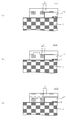
- FIG. 15 is a plan view showing a SAW device 401 according to the fifth embodiment.
- the outer periphery of the vibration space 21 (the inner wall 2a of the frame portion) is indicated by a dotted line.
- the SAW device 401 has a recess 10 in a predetermined region of the main surface 3a of the element substrate 3. As shown in FIG. 15, the recess 10 is provided so as to be exposed from the frame portion 2 when viewed in plan.
- FIG. 16 is a partial cross-sectional view taken along line XVI-XVI in FIG.
- the concave portion 10 is provided at a position just in contact with the outer wall 2b of the frame portion 2 when viewed in plan.
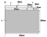
- FIG. 17 shows a reference analysis model S of the SAW device used for the simulation.
- the reference analysis model S is a simple model obtained by cutting out a part of a solid formed with the rotational symmetry axis A as a rotation axis.
- the material of the element substrate 3 is a lithium tantalate single crystal, and the cover 9 has a coefficient of thermal expansion at ⁇ 40 ° C. of 38.5 ppm / ° C. (actual value) and a coefficient of thermal expansion at 85 ° C. of 50 ppm / ° C. (actual value). Material.
- the dimensions of each part are as shown in FIG.
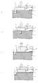
- the analysis models A to E were obtained by forming various recesses 10 or notches 13 in the SAW device of the reference analysis model S.
- the analysis model A is obtained by forming the concave portion 10 shown in FIG. 16 in the reference analysis model S, and the concave portion 10 is formed at a position in contact with the outer wall 2 b of the frame portion 2.
- the analysis model B is obtained by forming the concave portion 10 shown in FIG. 18A in the reference analysis model S.
- the concave portion 10 is partially located below the frame portion 2 and the remaining portion is the frame portion 2.
- the analysis model C is obtained by forming the concave portion 10 shown in FIG. 18B in the reference analysis model S, and the entire concave portion 10 is located below the frame portion 2.
- the analysis model D is obtained by forming the recess 10 shown in FIG.
- the analysis model E is a reference analysis model S in which notches 13 but notches 13 are formed.
- the notch 13 is formed so that the corner of the element substrate 3 is notched to the side surface starting from the portion of the outer wall 2b of the frame 2 that contacts the main surface of the element substrate 3.
- Table 1 shows the depth d and width w dimensions of the recess 10 or the notch 13 provided in each analysis model.
- the maximum principal stress applied to the cover 9 is smaller than that of the reference analysis model S in the analysis model A, analysis model B, analysis model D, and analysis model E other than the analysis model C. It was. On the other hand, the analysis model C has a maximum principal stress larger than that of the reference analysis model S.
- a part of the main surface 3a of the element substrate 3 is partly viewed in plan view in a region outside the portion located at the lower end of the inner wall 2a of the frame portion 2 that partitions the vibration space 21.
- the reason why the stress applied to the cover 9 can be reduced by forming the recess 10 or the notch 13 in this way is not necessarily clear, but one reason is that the thermal stress is relaxed. It is thought that.
- the cover 9 is changed according to the temperature change of the surrounding environment due to the difference in thermal expansion coefficient between the element substrate 3 and the cover 9. Thermal stress is generated.
- the concave portion 10 is provided as shown in FIG. 16, the element substrate 3 also follows the contraction indicated by the white arrow S1 of the cover 9 (frame part 2) as indicated by the white arrow S2. It is considered that the thermal stress of the cover 9 is reduced by some deformation.
- the interval between the edge of the recess 10 on the frame 2 side and the outer wall 2b of the frame 2 is 4 ⁇ m.
- the cover 9 The effect of relieving the stress generated by is reduced. From this, if the recessed part 10 or the notch part 13 is formed in the vicinity of the frame part 2, more specifically, the edge on the frame part 2 side is in contact with the frame part 2, the stress relaxation effect is enhanced. It is considered possible.
- the cross-sectional shape of the recess 10 is not limited to a rectangular shape as shown in FIGS. 16 and 18 (a) to (c), and may be a triangular shape as shown in FIG. 19 (a). As shown in FIG. 19B, the bottom may have an arc shape. Further, the cross-sectional shape of the cutout portion 13 is not limited to a triangular shape as shown in FIG. 18 (d), and for example, as shown in FIG. It may be what was.
- the formation position of the recessed part 10 or the notch part 13 is not restricted to what was shown in FIG. 15, For example, as shown in FIG. 20, you may form in each edge
- Such recesses 10 and notches 13 are formed in the above-described method of manufacturing the SAW device, for example, at the stage where the protective layer 8 shown in FIG. 5B is formed, the frame shown in FIG. At the stage where the portion 2 is formed or before the assembly of the wafer-like element substrate 3 before the cutting of the element substrate 3 in FIG. 6C, the main substrate of the element substrate 3 is obtained using a dicing blade or the like. It can be formed by making a cut in the surface 3a.
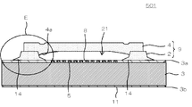
- FIG. 21 is a cross-sectional view showing a SAW device 501 of the sixth embodiment
- FIG. 22 is an enlarged view of a region E shown in FIG.
- the SAW device 501 in the sixth embodiment has an extending portion 14 at the lower end portion of the cover 9 (frame portion 2).
- the extending portion 14 extends along the main surface 3 a of the element substrate 3 on the outer surface side and the inner surface side of the joint portion of the cover 9 with the element substrate 3.
- the elongated portion 14 extends from the inner wall 2a toward the vibration space 21 on the inner wall 2a side of the frame portion 2, and extends from the outer wall 2b to the outer periphery of the element substrate 3 on the outer wall 2b side of the frame portion 2. It stretches toward.
- the extending portion 14 is provided over substantially the entire circumference of the lower end portion of the cover 9, but is not provided in the vicinity of the wiring 15.
- an infiltration path of moisture or the like to the vibrating space 21 between the cover 9 and the main surface 3a is increased by the amount of the extending portion 14, and thus the airtightness of the vibrating space 21 is increased.
- Sex can be maintained in a normal state for a long time. Therefore, corrosion of the excitation electrode 5 and the like in the vibration space can be suppressed, and the electrical characteristics of the SAW device 1 can be stabilized over a long period of time.
- the extending portion 14 is made of the same material as the cover 9 and is formed integrally with the cover 9, for example. If the extending portion 14 is formed integrally with the cover 9 in this way, the contact area on the main surface 3a side of the cover 9 can be considered to be increased by the amount of the extending portion 14, and thus the element substrate 3 of the cover 9 is moved to. The adhesion of the cover 9 can be improved, and the peeling of the cover 9 from the element substrate 3 can be suppressed. Note that the elongated portion 14 may be formed of a material different from that of the cover 9.
- the thick part such as the frame part 2 needs to be separated from the excitation electrode 5 and the element substrate 3 by a predetermined distance, and cannot be simply increased. This is because, on the excitation electrode 5 side, if a large thickness like the frame portion 2 touches the excitation electrode 5, the vibration of the excitation electrode 5 is greatly affected, resulting in deterioration of electrical characteristics. Since the portion of the substrate 3 is a wafer dicing line on the outer peripheral side of the substrate 3, if the thick frame portion 2 is present on the dicing line, chipping occurs in the element substrate 3 or the like when the wafer is cut.
- the SAW device 501 when the SAW device 501 is mounted on another mounting substrate and the entire SAW device 501 is covered with an exterior resin, the outer wall of the cover 9 is located near the outer periphery of the element substrate 2.
- the exterior resin is less likely to enter between the SAW device 1 and the main surface of the mounting substrate, and there is a problem that a gap is easily formed in that portion.
- the extension part 14 is formed so as to extend from the lower end part of the cover 9, it is assumed that the extension part 14 touches the excitation electrode 5 or extends to the vicinity of the outer periphery of the element substrate 3.
- the above problems are suppressed.
- the extension portion 14 is formed so that the thickness gradually decreases as it goes outward, even if the tip of the extension portion 14 touches the excitation electrode 5, the electrical characteristics are not greatly affected. Even if it extends to the vicinity of the outer periphery, it is possible to more effectively suppress the chipping of the element substrate 3 and the like during wafer dicing.
- the thickest portion of the extension portion 14, that is, the thickness of the connection portion with the cover 9, is, for example, 1/30 to 1/10 of the thickness of the frame portion 2.
- the thickness of the frame portion 2 is 30 ⁇ m
- the size of the thickest portion of the elongated portion 14 is 1.5 ⁇ m.
- the horizontal width of the extending portion 14 is, for example, about 40 ⁇ m.
- the cross-sectional shape of the elongated portion 14 is not limited to the triangular shape shown in FIG. 22, and the outer periphery may be an arc shape, a trapezoidal shape, a rectangular shape, or the like.
- 24A to 24C are enlarged cross-sectional views of a portion corresponding to FIG. 3, showing the SAW device 601 of the seventh embodiment.
- Each of the SAW devices 601 shown in FIGS. 24A to 24C has an uneven portion formed on the upper surface of the frame portion 2.
- an uneven portion that fits into the uneven portion formed in the frame portion 2 is formed on the lower surface of the lid portion 4, and when the lid portion 4 overlaps the frame portion 2, the uneven portion of the lid portion 4 is the frame portion. It fits in 2 uneven parts.
- the contact area between the lid 4 and the frame 2 is increased in the same manner as the hanging part 4 a in the SAW device 1 of the first embodiment described above. Therefore, it is possible to suppress the peeling between the lid portion 4 and the frame portion 2 and to prevent moisture from entering the vibration space 21 from the outside.
- the upper surface of the frame portion 2 is dry-etched at the stage of forming the frame portion 2 (FIG. 5D). Alternatively, it may be cut by wet etching.
- the frame portion 2 may have a two-layer structure. Specifically, the first layer below the convex portion is formed by the photolithography method or the like in the same manner as the case of forming the normal frame portion 2 (FIG. 5D), and then the upper layer of the first layer is formed.
- the second layer to be a convex portion may be formed by a photolithography method or the like.
- oxygen is formed on the upper surface of the frame body 2.
- An ashing process may be performed using plasma or the like.
- the uneven portion of the lid portion 4 that fits into the uneven portion formed on the upper surface of the frame portion 2 is, for example, the rotation of the roller 30 at the stage of attaching a thin film to be the lid portion 4 to the frame portion 2 (FIG. 6A). It can be formed by setting the speed, temperature, temperature of the stage 29, etc. to predetermined conditions.
- the cross-sectional shape of the concavo-convex portion is a rectangular shape, but the cross-sectional shape of the concavo-convex portion is not limited to this, for example, a triangular shape, a trapezoidal shape, an arc shape, etc. Any shape is possible.
- the depth of the concave portion in the concave and convex portion is, for example, 10% to 10% of the thickness of the frame portion 2 when relatively large concave and convex portions are formed as shown in FIGS. 60%, specifically 1 ⁇ m to 20 ⁇ m. Further, when relatively small irregularities are formed as shown in FIG.
- the upper surface of the frame portion 2 is roughened, and the arithmetic operation of the upper surface of the roughened frame portion 2 is performed.
- the average roughness (arithmetic average roughness as measured with a laser microscope) is 0.5 ⁇ m to 2 ⁇ m.
- the concavo-convex portions formed on the upper surface of the frame portion 2 may be formed so as to be evenly scattered on the upper surface of the frame portion 2 when the frame portion 2 is viewed in plan, or the concave portions are formed in the frame portion 2. You may form so that it may become a continuous groove
- the SAW device 1 according to the first embodiment also has a shape in which the frame-side uneven portion formed on the upper surface of the frame portion 2 and the lid-side uneven portion formed on the lower surface of the lid portion 4 are fitted. Can also be seen. That is, since the hanging part 4 a is formed on the lid part 4, a relatively large concave part is formed on the lower surface of the lid part 4, and a convex part that fits into the concave part is formed on the upper surface of the frame part 2. Can be seen.
- the present invention is not limited to the above embodiment, and may be implemented in various aspects, and the above-described embodiments may be combined as appropriate.
- an uneven portion is formed on the upper surface of the frame portion 2 like the SAW device 601 according to the sixth embodiment, and the lid portion 4 You may form the uneven
- the elastic wave device is not limited to a SAW device.
- the acoustic wave device may be a piezoelectric thin film resonator.
- the protective layer 8 and the back surface portion 11 are not essential requirements and may be omitted.
Landscapes
- Physics & Mathematics (AREA)
- Acoustics & Sound (AREA)
- Surface Acoustic Wave Elements And Circuit Networks Thereof (AREA)
Priority Applications (4)
| Application Number | Priority Date | Filing Date | Title |
|---|---|---|---|
| JP2012550237A JP5259024B1 (ja) | 2011-08-22 | 2012-08-22 | 弾性波装置および電子部品 |
| US14/239,768 US9548437B2 (en) | 2011-08-22 | 2012-08-22 | Acoustic wave device and electronic component |
| CN201280040419.9A CN103748787B (zh) | 2011-08-22 | 2012-08-22 | 弹性波装置以及电子部件 |
| US15/406,427 US10554192B2 (en) | 2011-08-22 | 2017-01-13 | Acoustic wave device and electronic component |
Applications Claiming Priority (6)
| Application Number | Priority Date | Filing Date | Title |
|---|---|---|---|
| JP2011-180265 | 2011-08-22 | ||
| JP2011180265 | 2011-08-22 | ||
| JP2011-239314 | 2011-10-31 | ||
| JP2011239314 | 2011-10-31 | ||
| JP2012-122994 | 2012-05-30 | ||
| JP2012122994 | 2012-05-30 |
Related Child Applications (2)
| Application Number | Title | Priority Date | Filing Date |
|---|---|---|---|
| US14/239,768 A-371-Of-International US9548437B2 (en) | 2011-08-22 | 2012-08-22 | Acoustic wave device and electronic component |
| US15/406,427 Continuation US10554192B2 (en) | 2011-08-22 | 2017-01-13 | Acoustic wave device and electronic component |
Publications (1)
| Publication Number | Publication Date |
|---|---|
| WO2013027760A1 true WO2013027760A1 (ja) | 2013-02-28 |
Family
ID=47746498
Family Applications (1)
| Application Number | Title | Priority Date | Filing Date |
|---|---|---|---|
| PCT/JP2012/071181 Ceased WO2013027760A1 (ja) | 2011-08-22 | 2012-08-22 | 弾性波装置および電子部品 |
Country Status (4)
| Country | Link |
|---|---|
| US (2) | US9548437B2 (enExample) |
| JP (5) | JP5259024B1 (enExample) |
| CN (1) | CN103748787B (enExample) |
| WO (1) | WO2013027760A1 (enExample) |
Cited By (10)
| Publication number | Priority date | Publication date | Assignee | Title |
|---|---|---|---|---|
| WO2016039038A1 (ja) * | 2014-09-09 | 2016-03-17 | 日本電波工業株式会社 | 圧電デバイス、圧電デバイス製造方法、及び電子部品 |
| JP2016123020A (ja) * | 2014-12-25 | 2016-07-07 | 京セラ株式会社 | 弾性波素子および通信装置 |
| JP2017147280A (ja) * | 2016-02-15 | 2017-08-24 | 株式会社デンソー | 電子回路部品 |
| CN107251428A (zh) * | 2015-03-27 | 2017-10-13 | 株式会社村田制作所 | 弹性波装置、通信模块设备以及弹性波装置的制造方法 |
| JPWO2016147724A1 (ja) * | 2015-03-16 | 2017-11-16 | 株式会社村田製作所 | 弾性表面波装置 |
| US20180110147A1 (en) * | 2013-11-08 | 2018-04-19 | Samsung Electro-Mechanics Co., Ltd. | Electronic component module and manufacturing method thereof |
| JP2018098599A (ja) * | 2016-12-12 | 2018-06-21 | 株式会社村田製作所 | 圧電振動子、モジュール部品及びそれらの製造方法 |
| JP2019062029A (ja) * | 2017-09-25 | 2019-04-18 | パナソニックIpマネジメント株式会社 | パッケージ用カバー部材、電子デバイス、及びパッケージ用カバー部材の製造方法 |
| JPWO2020262607A1 (enExample) * | 2019-06-28 | 2020-12-30 | ||
| US11653571B2 (en) | 2019-03-25 | 2023-05-16 | Seiko Epson Corporation | Resonance device, oscillator, resonance module, electronic device and vehicle |
Families Citing this family (22)
| Publication number | Priority date | Publication date | Assignee | Title |
|---|---|---|---|---|
| CN103748787B (zh) * | 2011-08-22 | 2017-04-12 | 京瓷株式会社 | 弹性波装置以及电子部件 |
| US10084168B2 (en) | 2012-10-09 | 2018-09-25 | Johnson Battery Technologies, Inc. | Solid-state battery separators and methods of fabrication |
| KR101706257B1 (ko) * | 2015-01-13 | 2017-02-13 | (주)와이솔 | 압전소자 디바이스 |
| JP6288533B2 (ja) * | 2015-05-27 | 2018-03-07 | 株式会社村田製作所 | 圧電振動子 |
| JP6612529B2 (ja) * | 2015-05-28 | 2019-11-27 | 京セラ株式会社 | 弾性波装置および通信装置 |
| JP6665487B2 (ja) * | 2015-11-02 | 2020-03-13 | セイコーエプソン株式会社 | 集積回路装置、電子デバイス、電子機器、および基地局 |
| US20170207766A1 (en) * | 2016-01-20 | 2017-07-20 | Qorvo Us, Inc. | Cap structure for wafer level package |
| WO2017139542A1 (en) | 2016-02-11 | 2017-08-17 | Skyworks Solutions, Inc. | Device packaging using a recyclable carrier substrate |
| US20170365554A1 (en) * | 2016-06-21 | 2017-12-21 | Skyworks Solutions, Inc. | Polymer bonding with improved step coverage |
| US10756700B2 (en) * | 2016-07-14 | 2020-08-25 | Samsung Electro-Mechanics Co., Ltd. | Bulk acoustic wave resonator device |
| WO2018021242A1 (ja) * | 2016-07-26 | 2018-02-01 | 京セラ株式会社 | 弾性波デバイスおよび通信装置 |
| US10453763B2 (en) | 2016-08-10 | 2019-10-22 | Skyworks Solutions, Inc. | Packaging structures with improved adhesion and strength |
| JP2018078419A (ja) * | 2016-11-08 | 2018-05-17 | 株式会社村田製作所 | 弾性波装置、高周波フロントエンド回路及び通信装置 |
| CN110100387B (zh) * | 2016-12-16 | 2023-06-06 | 株式会社村田制作所 | 弹性波装置、高频前端电路以及通信装置 |
| CN110089031B (zh) * | 2017-03-22 | 2024-02-23 | 京瓷株式会社 | 弹性波装置、分波器以及通信装置 |
| WO2019044178A1 (ja) * | 2017-08-31 | 2019-03-07 | 株式会社村田製作所 | 弾性波装置およびそれを備えた弾性波モジュール |
| DE112018006603B4 (de) * | 2017-12-26 | 2023-09-14 | Murata Manufacturing Co., Ltd. | Schallwellenvorrichtung und Schallwellenmodul |
| JP7057690B2 (ja) * | 2018-03-19 | 2022-04-20 | 株式会社村田製作所 | 弾性波装置 |
| DE102019115971A1 (de) * | 2019-06-12 | 2020-12-17 | RF360 Europe GmbH | Elektrisches Bauelement, elektrische Vorrichtung undVerfahren zur Herstellung einer Vielzahl von elektrischenBauelementen |
| TWI690156B (zh) | 2019-07-10 | 2020-04-01 | 頎邦科技股份有限公司 | 表面聲波裝置及其製造方法 |
| WO2021100506A1 (ja) | 2019-11-21 | 2021-05-27 | 株式会社村田製作所 | 電子部品 |
| CN117652098A (zh) * | 2021-07-08 | 2024-03-05 | 株式会社村田制作所 | 弹性波装置 |
Citations (3)
| Publication number | Priority date | Publication date | Assignee | Title |
|---|---|---|---|---|
| JP2008182292A (ja) * | 2007-01-23 | 2008-08-07 | Fujitsu Media Device Kk | 弾性波デバイス |
| JP2008235432A (ja) * | 2007-03-19 | 2008-10-02 | Fujitsu Media Device Kk | 電子部品およびその製造方法 |
| JP2010278971A (ja) * | 2009-06-01 | 2010-12-09 | Murata Mfg Co Ltd | 弾性波装置 |
Family Cites Families (22)
| Publication number | Priority date | Publication date | Assignee | Title |
|---|---|---|---|---|
| JPH04207308A (ja) * | 1990-11-30 | 1992-07-29 | Hitachi Ltd | 弾性表面波素子 |
| JP3748967B2 (ja) | 1996-12-02 | 2006-02-22 | Tdk株式会社 | 電子部品の封止構造 |
| JP4368499B2 (ja) * | 1999-06-14 | 2009-11-18 | パナソニック株式会社 | 弾性表面波素子の製造方法およびそれを用いた弾性表面波デバイスの製造方法 |
| JP2001217679A (ja) * | 2000-02-01 | 2001-08-10 | Murata Mfg Co Ltd | 端面反射型表面波装置、共用器及び通信機 |
| JP2001274271A (ja) | 2000-03-27 | 2001-10-05 | Kyocera Corp | 電子部品装置の製造方法 |
| JP4063000B2 (ja) * | 2001-08-14 | 2008-03-19 | 株式会社村田製作所 | 端面反射型表面波フィルタ |
| JP3783605B2 (ja) | 2001-10-29 | 2006-06-07 | 松下電器産業株式会社 | 気密封止パッケージおよびこれを用いたデバイス |
| JP4585419B2 (ja) * | 2005-10-04 | 2010-11-24 | 富士通メディアデバイス株式会社 | 弾性表面波デバイスおよびその製造方法 |
| JP2007318058A (ja) | 2006-04-27 | 2007-12-06 | Murata Mfg Co Ltd | 電子部品及びその製造方法 |
| JP5117083B2 (ja) | 2007-03-09 | 2013-01-09 | 太陽誘電株式会社 | 弾性波デバイスおよびその製造方法 |
| US8436514B2 (en) | 2007-10-30 | 2013-05-07 | Kyocera Corporation | Acoustic wave device comprising an inter-digital transducer electrode |
| US20110118339A1 (en) * | 2008-01-18 | 2011-05-19 | Alnylam Pharmaceuticals, Inc. | Chemically modified oligonucleotides and uses thereof |
| JP5104518B2 (ja) * | 2008-04-22 | 2012-12-19 | パナソニック株式会社 | 弾性表面波デバイスとその製造方法 |
| WO2009157587A1 (ja) | 2008-06-27 | 2009-12-30 | 京セラ株式会社 | 弾性波装置 |
| JP5434138B2 (ja) | 2009-02-27 | 2014-03-05 | パナソニック株式会社 | 弾性表面波部品およびその製造方法 |
| JP5532685B2 (ja) * | 2009-06-01 | 2014-06-25 | 株式会社村田製作所 | 弾性波装置 |
| JP5514478B2 (ja) * | 2009-06-26 | 2014-06-04 | 京セラ株式会社 | 弾性波装置及びその製造方法 |
| US9136195B2 (en) * | 2009-07-17 | 2015-09-15 | Tyco Electronics Corporation | Oxygen barrier compositions and related methods |
| JP5339313B2 (ja) | 2009-11-27 | 2013-11-13 | 京セラ株式会社 | 弾性波装置およびその製造方法 |
| JP5339625B2 (ja) * | 2009-12-21 | 2013-11-13 | 太陽誘電株式会社 | 中空パッケージの製造方法 |
| JP2011188255A (ja) * | 2010-03-09 | 2011-09-22 | Panasonic Corp | 弾性波素子 |
| CN103748787B (zh) * | 2011-08-22 | 2017-04-12 | 京瓷株式会社 | 弹性波装置以及电子部件 |
-
2012
- 2012-08-22 CN CN201280040419.9A patent/CN103748787B/zh active Active
- 2012-08-22 WO PCT/JP2012/071181 patent/WO2013027760A1/ja not_active Ceased
- 2012-08-22 JP JP2012550237A patent/JP5259024B1/ja active Active
- 2012-08-22 US US14/239,768 patent/US9548437B2/en active Active
- 2012-11-06 JP JP2012244333A patent/JP5926165B2/ja active Active
-
2013
- 2013-02-14 JP JP2013026324A patent/JP5859993B2/ja active Active
-
2016
- 2016-04-21 JP JP2016085183A patent/JP6396941B2/ja active Active
-
2017
- 2017-01-13 US US15/406,427 patent/US10554192B2/en active Active
-
2018
- 2018-08-30 JP JP2018161728A patent/JP6603377B2/ja active Active
Patent Citations (3)
| Publication number | Priority date | Publication date | Assignee | Title |
|---|---|---|---|---|
| JP2008182292A (ja) * | 2007-01-23 | 2008-08-07 | Fujitsu Media Device Kk | 弾性波デバイス |
| JP2008235432A (ja) * | 2007-03-19 | 2008-10-02 | Fujitsu Media Device Kk | 電子部品およびその製造方法 |
| JP2010278971A (ja) * | 2009-06-01 | 2010-12-09 | Murata Mfg Co Ltd | 弾性波装置 |
Cited By (16)
| Publication number | Priority date | Publication date | Assignee | Title |
|---|---|---|---|---|
| US10667419B2 (en) * | 2013-11-08 | 2020-05-26 | Samsung Electro-Mechanics Co., Ltd. | Manufacturing method of an electronic component module |
| US20180110147A1 (en) * | 2013-11-08 | 2018-04-19 | Samsung Electro-Mechanics Co., Ltd. | Electronic component module and manufacturing method thereof |
| WO2016039038A1 (ja) * | 2014-09-09 | 2016-03-17 | 日本電波工業株式会社 | 圧電デバイス、圧電デバイス製造方法、及び電子部品 |
| JP2016123020A (ja) * | 2014-12-25 | 2016-07-07 | 京セラ株式会社 | 弾性波素子および通信装置 |
| JPWO2016147724A1 (ja) * | 2015-03-16 | 2017-11-16 | 株式会社村田製作所 | 弾性表面波装置 |
| CN107251428A (zh) * | 2015-03-27 | 2017-10-13 | 株式会社村田制作所 | 弹性波装置、通信模块设备以及弹性波装置的制造方法 |
| JPWO2016158050A1 (ja) * | 2015-03-27 | 2017-10-26 | 株式会社村田製作所 | 弾性波装置、通信モジュール機器及び弾性波装置の製造方法 |
| CN107251428B (zh) * | 2015-03-27 | 2020-10-23 | 株式会社村田制作所 | 弹性波装置、通信模块设备以及弹性波装置的制造方法 |
| JP2017147280A (ja) * | 2016-02-15 | 2017-08-24 | 株式会社デンソー | 電子回路部品 |
| US10938370B2 (en) | 2016-12-12 | 2021-03-02 | Murata Manufacturing Co., Ltd. | Piezoelectric resonator unit, module component, and manufacturing method for same |
| JP2018098599A (ja) * | 2016-12-12 | 2018-06-21 | 株式会社村田製作所 | 圧電振動子、モジュール部品及びそれらの製造方法 |
| JP2019062029A (ja) * | 2017-09-25 | 2019-04-18 | パナソニックIpマネジメント株式会社 | パッケージ用カバー部材、電子デバイス、及びパッケージ用カバー部材の製造方法 |
| JP7029691B2 (ja) | 2017-09-25 | 2022-03-04 | パナソニックIpマネジメント株式会社 | パッケージ用カバー部材、電子デバイス、及びパッケージ用カバー部材の製造方法 |
| US11653571B2 (en) | 2019-03-25 | 2023-05-16 | Seiko Epson Corporation | Resonance device, oscillator, resonance module, electronic device and vehicle |
| JPWO2020262607A1 (enExample) * | 2019-06-28 | 2020-12-30 | ||
| JP7344290B2 (ja) | 2019-06-28 | 2023-09-13 | 京セラ株式会社 | 弾性波装置及び弾性波装置の製造方法 |
Also Published As
| Publication number | Publication date |
|---|---|
| JP6396941B2 (ja) | 2018-09-26 |
| US20170207767A1 (en) | 2017-07-20 |
| JPWO2013027760A1 (ja) | 2015-03-19 |
| JP2018207524A (ja) | 2018-12-27 |
| JP2014007722A (ja) | 2014-01-16 |
| US20140191617A1 (en) | 2014-07-10 |
| JP2014007727A (ja) | 2014-01-16 |
| JP6603377B2 (ja) | 2019-11-06 |
| US9548437B2 (en) | 2017-01-17 |
| US10554192B2 (en) | 2020-02-04 |
| JP2016171579A (ja) | 2016-09-23 |
| JP5926165B2 (ja) | 2016-05-25 |
| CN103748787A (zh) | 2014-04-23 |
| JP5259024B1 (ja) | 2013-08-07 |
| CN103748787B (zh) | 2017-04-12 |
| JP5859993B2 (ja) | 2016-02-16 |
Similar Documents
| Publication | Publication Date | Title |
|---|---|---|
| JP6603377B2 (ja) | 弾性波装置および電子部品 | |
| JP5882306B2 (ja) | 電子部品 | |
| CN101911485B (zh) | 压电器件 | |
| JP5591163B2 (ja) | 弾性波装置およびその製造方法 | |
| JP5815365B2 (ja) | 弾性波装置、電子部品および弾性波装置の製造方法 | |
| JP5688149B2 (ja) | 弾性波装置を有する電子部品 | |
| JP5730169B2 (ja) | 弾性波装置、電子部品および弾性波装置の製造方法 | |
| JP5721500B2 (ja) | 弾性波装置およびその製造方法 | |
| JP6298120B2 (ja) | 弾性波装置および回路基板 | |
| JP5865698B2 (ja) | 弾性波装置、電子部品および弾性波装置の製造方法 | |
| JP2013118444A (ja) | 弾性波デバイスの製造方法及び弾性波デバイス | |
| JP6142023B2 (ja) | 弾性波装置、電子部品および弾性波装置の製造方法 | |
| JP5813177B2 (ja) | 弾性波装置および回路基板 | |
| JP5754907B2 (ja) | 弾性波装置および回路基板 | |
| JP5945016B2 (ja) | 弾性波装置、電子部品および弾性波装置の製造方法 | |
| JP5997327B2 (ja) | 弾性波装置および回路基板 | |
| JP4186677B2 (ja) | 弾性表面波装置及びその製造方法 | |
| JP2018093528A (ja) | 弾性波装置および回路基板 |
Legal Events
| Date | Code | Title | Description |
|---|---|---|---|
| ENP | Entry into the national phase |
Ref document number: 2012550237 Country of ref document: JP Kind code of ref document: A |
|
| 121 | Ep: the epo has been informed by wipo that ep was designated in this application |
Ref document number: 12825025 Country of ref document: EP Kind code of ref document: A1 |
|
| WWE | Wipo information: entry into national phase |
Ref document number: 14239768 Country of ref document: US |
|
| NENP | Non-entry into the national phase |
Ref country code: DE |
|
| 122 | Ep: pct application non-entry in european phase |
Ref document number: 12825025 Country of ref document: EP Kind code of ref document: A1 |