WO2012161218A1 - 配線板および配線板の製造方法 - Google Patents
配線板および配線板の製造方法 Download PDFInfo
- Publication number
- WO2012161218A1 WO2012161218A1 PCT/JP2012/063186 JP2012063186W WO2012161218A1 WO 2012161218 A1 WO2012161218 A1 WO 2012161218A1 JP 2012063186 W JP2012063186 W JP 2012063186W WO 2012161218 A1 WO2012161218 A1 WO 2012161218A1
- Authority
- WO
- WIPO (PCT)
- Prior art keywords
- hole
- metal plate
- base material
- wiring board
- plate
- Prior art date
Links
Images


Classifications
-
- H—ELECTRICITY
- H05—ELECTRIC TECHNIQUES NOT OTHERWISE PROVIDED FOR
- H05K—PRINTED CIRCUITS; CASINGS OR CONSTRUCTIONAL DETAILS OF ELECTRIC APPARATUS; MANUFACTURE OF ASSEMBLAGES OF ELECTRICAL COMPONENTS
- H05K1/00—Printed circuits
- H05K1/02—Details
- H05K1/11—Printed elements for providing electric connections to or between printed circuits
-
- H—ELECTRICITY
- H05—ELECTRIC TECHNIQUES NOT OTHERWISE PROVIDED FOR
- H05K—PRINTED CIRCUITS; CASINGS OR CONSTRUCTIONAL DETAILS OF ELECTRIC APPARATUS; MANUFACTURE OF ASSEMBLAGES OF ELECTRICAL COMPONENTS
- H05K3/00—Apparatus or processes for manufacturing printed circuits
- H05K3/0094—Filling or covering plated through-holes or blind plated vias, e.g. for masking or for mechanical reinforcement
-
- H—ELECTRICITY
- H05—ELECTRIC TECHNIQUES NOT OTHERWISE PROVIDED FOR
- H05K—PRINTED CIRCUITS; CASINGS OR CONSTRUCTIONAL DETAILS OF ELECTRIC APPARATUS; MANUFACTURE OF ASSEMBLAGES OF ELECTRICAL COMPONENTS
- H05K3/00—Apparatus or processes for manufacturing printed circuits
- H05K3/40—Forming printed elements for providing electric connections to or between printed circuits
- H05K3/4038—Through-connections; Vertical interconnect access [VIA] connections
- H05K3/4084—Through-connections; Vertical interconnect access [VIA] connections by deforming at least one of the conductive layers
-
- H—ELECTRICITY
- H05—ELECTRIC TECHNIQUES NOT OTHERWISE PROVIDED FOR
- H05K—PRINTED CIRCUITS; CASINGS OR CONSTRUCTIONAL DETAILS OF ELECTRIC APPARATUS; MANUFACTURE OF ASSEMBLAGES OF ELECTRICAL COMPONENTS
- H05K1/00—Printed circuits
- H05K1/02—Details
- H05K1/0213—Electrical arrangements not otherwise provided for
- H05K1/0263—High current adaptations, e.g. printed high current conductors or using auxiliary non-printed means; Fine and coarse circuit patterns on one circuit board
-
- H—ELECTRICITY
- H05—ELECTRIC TECHNIQUES NOT OTHERWISE PROVIDED FOR
- H05K—PRINTED CIRCUITS; CASINGS OR CONSTRUCTIONAL DETAILS OF ELECTRIC APPARATUS; MANUFACTURE OF ASSEMBLAGES OF ELECTRICAL COMPONENTS
- H05K1/00—Printed circuits
- H05K1/02—Details
- H05K1/11—Printed elements for providing electric connections to or between printed circuits
- H05K1/115—Via connections; Lands around holes or via connections
-
- H—ELECTRICITY
- H05—ELECTRIC TECHNIQUES NOT OTHERWISE PROVIDED FOR
- H05K—PRINTED CIRCUITS; CASINGS OR CONSTRUCTIONAL DETAILS OF ELECTRIC APPARATUS; MANUFACTURE OF ASSEMBLAGES OF ELECTRICAL COMPONENTS
- H05K2201/00—Indexing scheme relating to printed circuits covered by H05K1/00
- H05K2201/03—Conductive materials
- H05K2201/0302—Properties and characteristics in general
- H05K2201/0305—Solder used for other purposes than connections between PCB or components, e.g. for filling vias or for programmable patterns
-
- H—ELECTRICITY
- H05—ELECTRIC TECHNIQUES NOT OTHERWISE PROVIDED FOR
- H05K—PRINTED CIRCUITS; CASINGS OR CONSTRUCTIONAL DETAILS OF ELECTRIC APPARATUS; MANUFACTURE OF ASSEMBLAGES OF ELECTRICAL COMPONENTS
- H05K2201/00—Indexing scheme relating to printed circuits covered by H05K1/00
- H05K2201/09—Shape and layout
- H05K2201/09209—Shape and layout details of conductors
- H05K2201/095—Conductive through-holes or vias
- H05K2201/09509—Blind vias, i.e. vias having one side closed
-
- H—ELECTRICITY
- H05—ELECTRIC TECHNIQUES NOT OTHERWISE PROVIDED FOR
- H05K—PRINTED CIRCUITS; CASINGS OR CONSTRUCTIONAL DETAILS OF ELECTRIC APPARATUS; MANUFACTURE OF ASSEMBLAGES OF ELECTRICAL COMPONENTS
- H05K2201/00—Indexing scheme relating to printed circuits covered by H05K1/00
- H05K2201/09—Shape and layout
- H05K2201/09209—Shape and layout details of conductors
- H05K2201/09654—Shape and layout details of conductors covering at least two types of conductors provided for in H05K2201/09218 - H05K2201/095
- H05K2201/0969—Apertured conductors
-
- H—ELECTRICITY
- H05—ELECTRIC TECHNIQUES NOT OTHERWISE PROVIDED FOR
- H05K—PRINTED CIRCUITS; CASINGS OR CONSTRUCTIONAL DETAILS OF ELECTRIC APPARATUS; MANUFACTURE OF ASSEMBLAGES OF ELECTRICAL COMPONENTS
- H05K2203/00—Indexing scheme relating to apparatus or processes for manufacturing printed circuits covered by H05K3/00
- H05K2203/03—Metal processing
- H05K2203/033—Punching metal foil, e.g. solder foil
-
- H—ELECTRICITY
- H05—ELECTRIC TECHNIQUES NOT OTHERWISE PROVIDED FOR
- H05K—PRINTED CIRCUITS; CASINGS OR CONSTRUCTIONAL DETAILS OF ELECTRIC APPARATUS; MANUFACTURE OF ASSEMBLAGES OF ELECTRICAL COMPONENTS
- H05K2203/00—Indexing scheme relating to apparatus or processes for manufacturing printed circuits covered by H05K3/00
- H05K2203/11—Treatments characterised by their effect, e.g. heating, cooling, roughening
- H05K2203/1178—Means for venting or for letting gases escape
-
- H—ELECTRICITY
- H05—ELECTRIC TECHNIQUES NOT OTHERWISE PROVIDED FOR
- H05K—PRINTED CIRCUITS; CASINGS OR CONSTRUCTIONAL DETAILS OF ELECTRIC APPARATUS; MANUFACTURE OF ASSEMBLAGES OF ELECTRICAL COMPONENTS
- H05K3/00—Apparatus or processes for manufacturing printed circuits
- H05K3/40—Forming printed elements for providing electric connections to or between printed circuits
- H05K3/4038—Through-connections; Vertical interconnect access [VIA] connections
- H05K3/4046—Through-connections; Vertical interconnect access [VIA] connections using auxiliary conductive elements, e.g. metallic spheres, eyelets, pieces of wire
-
- Y—GENERAL TAGGING OF NEW TECHNOLOGICAL DEVELOPMENTS; GENERAL TAGGING OF CROSS-SECTIONAL TECHNOLOGIES SPANNING OVER SEVERAL SECTIONS OF THE IPC; TECHNICAL SUBJECTS COVERED BY FORMER USPC CROSS-REFERENCE ART COLLECTIONS [XRACs] AND DIGESTS
- Y10—TECHNICAL SUBJECTS COVERED BY FORMER USPC
- Y10T—TECHNICAL SUBJECTS COVERED BY FORMER US CLASSIFICATION
- Y10T29/00—Metal working
- Y10T29/49—Method of mechanical manufacture
- Y10T29/49002—Electrical device making
- Y10T29/49117—Conductor or circuit manufacturing
- Y10T29/49124—On flat or curved insulated base, e.g., printed circuit, etc.
- Y10T29/49155—Manufacturing circuit on or in base
- Y10T29/49165—Manufacturing circuit on or in base by forming conductive walled aperture in base
Definitions
- the present invention relates to a wiring board and a method for manufacturing the wiring board.
- the interlayer connection in the substrate is generally performed by copper plating.
- a copper plating layer 304 formed on the inner wall surface of the through hole 303 is formed between the front surface layer (for example, copper foil) 301 and the back surface layer (for example, copper foil) 302 on the insulating substrate 300. Connecting.
- a large current for example, 120 amperes
- Patent Document 1 discloses a technique for flowing a large current. Specifically, in the printed wiring board, a plurality of current through holes penetrating the front surface side and the back surface side of the substrate are arranged densely. As a result, a large current of 50 to 180 amperes can be passed without using a bus bar.
- An object of the present invention is to provide a wiring board and wiring capable of flowing a large current through a conductive path connecting a metal plate on the front surface and a metal plate on the back surface and reducing the amount of conductive material constituting the conductive path. It is in providing the manufacturing method of a board.
- a wiring board is bonded to a substrate having a front surface, a back surface, and a side surface, a first metal plate bonded to the surface, and the back surface.
- a second metal plate, and a conductive path configured to conduct between the first metal plate and the second metal plate.
- the conductive path is provided in an internal space defined by an inner wall surface of a base material through-hole formed in the base material or an external space outside the side surface of the base material.
- the conductive path includes the first metal plate, the second metal plate, and a conductive material that electrically connects the first metal plate and the second metal plate.
- At least one of the first metal plate and the second metal plate is joined to the base material, and a bent portion extending so as to be bent from the joint portion so as to cover the inner wall surface or the side surface. And have.
- the inside of the bent part is filled with the conductive material.
- At least one of the first metal plate and the second metal plate is bent from the joint portion so as to cover the joint portion joined to the base material and the inner wall surface or the side surface. It has a bent part that extends. A conductive material is filled in the inner portion of the bent portion.
- the conductive path electrically connects the first metal plate joined to the surface of the base material, the second metal plate joined to the back surface of the base material, the first metal plate and the second metal plate. And a conductive material to be connected.
- the first metal plate and the second metal plate conduct in the internal space of the base material through hole penetrating the base material or the external space outside the side surface of the base material. Thereby, a big electric current can be sent through the conductive path which connects a 1st metal plate and a 2nd metal plate.
- the space filled with the conductive material is narrowed, the amount of the conductive material to be filled can be reduced.
- the first metal plate includes a first joint as the joint and a first bent part as the bent part.
- the first bent portion bends toward the back surface.
- the second metal plate has a second joint portion as the joint portion and a second bent portion as the bent portion.
- the second bent portion is bent toward the surface so as to cover the inner wall surface or the side surface together with the first bent portion.
- the conductive material is filled between the first bent portion and the second bent portion.
- the place where the conductive material is filled is between the first bent portion that is bent toward the back surface of the base material and the second bent portion that is bent toward the surface of the base material, Since the bent portion and the second bent portion are bent toward the base material side, it is easy to flow downward after the conductive material is melted.
- the second metal plate has a through hole at a portion facing the internal space or the external space.
- the conductive path is provided in the internal space.
- the first bent portion bends from the opening end of the base material through hole that opens to the surface toward the internal space, and has a through hole at a portion corresponding to the central portion of the base material through hole. ing.
- the second bent portion is bent toward the internal space from the opening end of the base material through hole that opens to the back surface, and is inserted into the through hole of the first bent portion.
- a plurality of the through holes formed in the second metal plate are provided on a circumference around the central axis of the base material through hole having a circular cross section.
- the conductive path can be more reliably inspected by a plurality of through holes provided on the circumference around the central axis of the base material through hole having a circular cross section.
- the plurality of through holes formed in the second metal plate are arranged at equiangular intervals.
- the conductive path can be inspected more reliably.
- the wiring board according to the second aspect of the present invention includes a base material having a front surface, a back surface, and a base material through hole, a first metal plate bonded to the front surface, and a second metal bonded to the back surface.
- a metal plate and a conductive path provided in the internal space of the through hole so as to conduct electricity between the first metal plate and the second metal plate.
- the conductive path includes the first metal plate, the second metal plate, and a conductive material that electrically connects the first metal plate and the second metal plate.
- the second metal plate has a joint portion joined to the base material and an extending portion extending from the joint portion to the opening portion of the base material through hole.
- a plate material having a through hole is disposed in the internal space. The conductive material is filled in the through holes of the plate material.
- the second metal plate has the joint portion joined to the base material and the extending portion extending from the joint portion to the opening portion of the base material through hole.
- a plate material having a through hole is disposed in the internal space of the substrate through hole.
- a conductive material is filled in the through hole of the plate material.
- the conductive path electrically connects the first metal plate joined to the surface of the base material, the second metal plate joined to the back surface of the base material, the first metal plate and the second metal plate. And a conductive material to be connected.
- the first metal plate and the second metal plate conduct in the internal space of the base material through hole penetrating the base material. Thereby, a big electric current can be sent through the conductive path which connects a 1st metal plate and a 2nd metal plate.
- the space filled with the conductive material is narrowed by the plate material disposed in the space filled with the conductive material, the amount of the conductive material to be filled can be reduced.
- the extending portion has a through hole communicating with the through hole of the plate member.
- the first metal plate has a joint part joined to the base material and an extending part extending from the joint part to the opening of the base material through hole.
- the extending portion has a through hole smaller than the base material through hole.
- the through hole of the plate material communicates with the through hole of the first metal plate, and the conductive material is filled into the through hole of the first metal plate and the through hole of the plate material.
- the wiring board is bonded to the base having a front surface, a back surface, and a side surface, a first metal plate bonded to the front surface, and the back surface.
- a second metal plate and a conductive path configured to conduct between the first metal plate and the second metal plate, the conductive path being a base material formed on the base material Provided in an internal space defined by an inner wall surface of the through hole, the conductive path includes the first metal plate, the second metal plate, the first metal plate, and the second metal plate. And a conductive material that electrically connects the conductive paths.
- At least one of the first metal plate and the second metal plate has a joint part joined to the base material and a bent part extending to bend from the joint part so as to cover the inner wall surface.
- the method for manufacturing the wiring board includes a step of bonding the first metal plate to the front surface, and a step of bonding the second metal plate to the back surface so as to block one opening end of the base material through hole.
- the first metal plate is joined to the surface of the base material, and the second metal plate closes one opening end of the base material through hole on the back surface of the base material Are joined together.
- a solder paste is applied to a portion corresponding to the other opening end of the base material through hole on the surface of the first metal plate.
- the solder paste is reflowed and the inside of the bent portion including the inside of the through hole is removed as a conductive material while the gas is extracted from the through hole formed in the part facing the base material internal space in the second metal plate. Solder is filled.
- Solder wettability is stabilized by removing the gas from the substrate through-holes in the reflow process in manufacturing the wiring board.
- the wiring board is bonded to the base having a front surface, a back surface, and a side surface, a first metal plate bonded to the front surface, and the back surface.
- a second metal plate, and a conductive path configured to conduct between the first metal plate and the second metal plate.
- the conductive path is provided in an internal space defined by an inner wall surface of a base material through hole formed in the base material, and the conductive path includes the first metal plate, the second metal plate, and the A conductive material that electrically connects the first metal plate and the second metal plate.
- the method of manufacturing the wiring board is a step of arranging the second metal plate having a through hole on the back surface, and the through hole of the second metal plate corresponds to the opening of the base material through hole.
- the through hole of the first metal plate communicates with the through hole of the plate material, the process, the through hole of the second metal plate, the through hole of the first metal plate, and the penetration of the plate material. Filling the space formed by the holes with solder as a conductive material , Comprising a.
- the second metal plate is disposed on the back surface of the base material and has a through hole that is located at the opening of the base material through hole and is smaller than the base material through hole. Is done.
- a plate material that is communicated with the through hole of the second metal plate and has a through hole larger than the through hole of the second metal plate is arranged inside the base material through hole.
- a first metal plate in which a through hole communicating with the through hole of the plate material is formed on the surface of the substrate.
- solder as a conductive material is filled in the through hole of the first metal plate including the inside of the through hole of the second metal plate and the internal space of the through hole of the plate material.
- the wiring board according to the second aspect can be obtained.
- a large current can be passed through the conductive path connecting the front and back, and the amount of conductive material constituting the conductive path can be reduced.
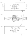
- (A) is a plan view of the wiring board according to the first embodiment of the present invention
- (b) is a longitudinal sectional view taken along line II in FIG. 1 (a)
- (c) is a bottom view of the wiring board.
- (A) is a plan view of the wiring board for explaining the manufacturing process of the wiring board of FIG. 1 (a)
- (b) is a longitudinal sectional view taken along line II-II of (a)
- (c) is wiring.
- (A) is a plan view of the wiring board for explaining the manufacturing process of the wiring board of FIG. 1,
- (b) is a longitudinal sectional view taken along line III-III of (a)
- (c) is a lower surface of the wiring board.
- FIG. 1 is a plan view of the wiring board for explaining the manufacturing process of the wiring board of FIG. 1
- (b) is a longitudinal sectional view taken along line IV-IV of (a)
- (c) is a lower surface of the wiring board.
- Figure. (A) is a top view of the wiring board based on the 2nd Embodiment of this invention
- (b) is a longitudinal cross-sectional view along the VV line of (a)
- (c) is a bottom view of a wiring board.
- 5A is a plan view of the wiring board for explaining the manufacturing process of the wiring board of FIG. 5A
- FIG. 5B is a longitudinal sectional view taken along line VI-VI of FIG. 5A
- FIG. 5A is a plan view of the wiring board for explaining the manufacturing process of the wiring board in FIG. 5
- FIG. 5B is a longitudinal sectional view taken along line VII-VII in FIG. 5A
- FIG. Figure. 5A is a plan view of the wiring board for explaining the manufacturing process of the wiring board of FIG. 5
- FIG. 5B is a longitudinal sectional view taken along line VIII-VIII of FIG. 5A
- FIG. Figure. (A) is a top view of the wiring board based on the 3rd Embodiment of this invention
- (b) is a longitudinal cross-sectional view along the IX-IX line of (a)
- (c) is a bottom view of a wiring board.
- FIG. 9A is a plan view of the wiring board for explaining the manufacturing process of the wiring board of FIG. 9A
- FIG. 9B is a longitudinal sectional view taken along line XX of FIG. 9A
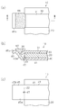
- (A) is a top view of the wiring board based on the 4th Embodiment of this invention
- (b) is a longitudinal cross-sectional view along the XI-XI line of (a)
- (c) is a bottom view of a wiring board.
- (A)-(c) is a longitudinal cross-sectional view of a wiring board for demonstrating the manufacturing process of the wiring board of Fig.11 (a).
- (A), (b) is a longitudinal cross-sectional view of a wiring board for demonstrating the manufacturing process of the wiring board of Fig.11 (a). The longitudinal cross-sectional view of the wiring board for a comparison.
- (A)-(c) is a longitudinal cross-sectional view for demonstrating the application
- (A)-(c) is a longitudinal cross-sectional view for demonstrating the application process of the solder paste for a comparison.
- (A)-(c) is a longitudinal cross-sectional view for demonstrating the manufacturing process of a modification.
- the wiring board 10 is configured using a thick copper substrate. That is, the first copper plate 30 as the first metal plate is bonded to the upper surface of the insulating substrate 20 as the base material. A second copper plate 40 as a second metal plate is bonded to the lower surface of the insulating substrate 20. The first copper plate 30 is patterned into a desired shape to form a current path. Further, the second copper plate 40 is patterned into a desired shape to form a current path.
- a glass / epoxy resin substrate can be used for the insulating substrate 20.
- the thickness of the insulating substrate 20 is 400 ⁇ m, for example, the thickness of the first copper plate 30 is 500 ⁇ m, for example, and the thickness of the second copper plate 40 is 500 ⁇ m, for example.
- the conductor pattern made of the first copper plate 30 and the conductor pattern made of the second copper plate 40 are electrically connected in the following configuration.
- the wiring board 10 is bonded to the first copper plate 30 bonded to the front surface (upper surface) of the insulating substrate 20 and the rear surface (lower surface) of the insulating substrate 20 inside the base material through hole 21 penetrating the insulating substrate 20.
- a conductive path 50 is formed to conduct with the second copper plate 40 to be formed.
- the base material through-hole 21 is circular.
- the conductive path 50 includes a first copper plate 30, a second copper plate 40, and a solder 60 as a conductive material that electrically connects the first copper plate 30 and the second copper plate 40.
- the first copper plate 30 has a first bent portion 32.
- the first bent portion 32 extends from the first joint portion 31 and is bent toward the back surface side (lower surface side) of the insulating substrate 20. Specifically, the first bent portion 32 is bent into the inside of the base material through hole 21 from the opening portion on the surface side (upper surface side) of the insulating substrate 20 in the base material through hole 21. The first bent portion 32 linearly extends obliquely downward from the opening of the substrate through hole 21.
- a through hole 33 is formed at a portion corresponding to the central portion of the base material through hole 21 in the first bent portion 32. The through hole 33 is circular.
- Two through holes 43 and 44 are formed in the second copper plate 40, and the second copper plate 40 has a second bent portion 42, and the second bent portion 42 has a first bent portion 42.
- the second joint 41 extends from the second joint 41.
- the second bent portion 42 is formed at a portion corresponding to the central portion of the base material through hole 21.
- the second bent portion 42 has a slanted portion 42a and a horizontal portion 42b.
- the second bent part 42 is arranged so as to bend toward the surface side (upper surface side) of the insulating substrate 20 and to cover the inner wall surface of the substrate through-hole 21 together with the first bent part 32.
- the inclined portion 42 a of the second bent portion 42 is obliquely upward from the opening on the back surface side (lower surface side) of the insulating substrate 20 in the base material through hole 21 toward the inside of the base material through hole 21. It is bent so as to extend linearly and is inserted into the through hole 33 of the first bent portion 32.
- a horizontal portion 42b is located at the tip of the inclined portion 42a.
- the horizontal portion 42b is circular in plan view, and the upper surface of the horizontal portion 42b is a horizontal plane.
- the upper surface of the horizontal portion 42b is slightly lower than the upper surface of the wiring board 10 (the upper surface of the first copper plate 30).
- the through holes 43 and 44 are provided in a portion of the second copper plate 40 facing the inside of the base material through hole 21. Specifically, the through holes 43 and 44 are formed between the outer periphery of the opening of the base material through hole 21 in the second copper plate 40 and the root portion of the second bent part 42. More specifically, the through holes 43 and 44 are formed in a portion closer to the inclined portion 42a in the second copper plate 40.
- the two through holes 43 and 44 are provided on the circumference centering on the center O of the circular base material through hole 21.
- the through holes (43, 44) are arranged at equiangular intervals.
- the through holes 43 and 44 are circular.
- solder 60 is filled in the space between the first bent part 32 and the second bent part 42 including the inside of the through holes 43 and 44. It can be visually observed that the solder 60 is poured by the through holes 43 and 44, that is, it can be ensured that the solder 60 is poured by the through holes 43 and 44.
- a first copper plate 30 is bonded to the surface of the insulating substrate 20 and a second copper plate 40 is bonded to the back surface of the insulating substrate 20.
- the space between the first bent part 32 and the second bent part 42 is filled with solder 60.
- the first copper plate 30 and the second copper plate 40 are electrically connected to each other by the solder 60.
- a current I flows from the first copper plate 30 to the second copper plate 40. Specifically, a current flows from the first bent portion 32 to the second bent portion 42 through the solder 60. At this time, a large current (for example, 120 amperes) can be passed.
- a large current for example, 120 amperes
- a large current for example, 120 amperes
- an insulating substrate 20, a first copper plate 30, and a second copper plate 40 are prepared.
- a base material through hole 21 is formed in the insulating substrate 20.
- a first bent portion 32 is formed on the first copper plate 30.
- a second bent portion 42 is formed on the second copper plate 40.
- the first copper plate 30 is bonded to the upper surface of the insulating substrate 20 and the second copper plate 40 is bonded to the lower surface of the insulating substrate 20.
- the first bent portion 32 of the first copper plate 30 is positioned in the base material through hole 21 of the insulating substrate 20.
- the second bent portion 42 of the second copper plate 40 is arranged in the base material through hole 21 of the insulating substrate 20 so as to cover the inner wall surface of the base material through hole 21 together with the first bent portion 32.
- a gap is formed between the first bent portion 32 and the second bent portion 42, and this gap is a space for filling the solder 60.
- the solder paste 61 is applied to the formation region of the through hole 33 (on the horizontal portion 42 b of the second bent portion 42) and the periphery thereof in the first copper plate 30.
- the application of the solder paste 61 is performed in a state where the region other than the application region of the solder paste 61 in the substrate through hole 21 is covered with a metal mask. That is, the upper surface of the wiring board 10 is flat, and a copper plate surface having no protrusion is secured, so that the solder paste can be printed in a desired region.
- the solder paste is applied also in the area where the surface mount component is arranged in the area other than the double-sided connection part (base material through hole 21) in the wiring board 10.
- the solder having fluidity flows between the first bent portion 32 and the second bent portion 42 below the application region of the solder paste 61. As shown in FIG. 1, the space between the first bent portion 32 and the second bent portion 42 is filled with the solder 60. In addition, the solder 60 is filled in the through holes 43 and 44.
- the reflow solder 60 is sufficiently between the first bent portion 32 and the second bent portion 42. It can be seen that it is contained, and the quality of soldering can be judged. Specifically, since the second copper plate 40 has a red-black color and the solder 60 has a silver color, it can be easily identified. Thereby, a connection can be guaranteed.
- the solder 60 when the solder 60 is filled between the first bent portion 32 and the second bent portion 42, the solder 60 is filled in the through holes 43 and 44. If not, it will look like this: The solder 60 cannot be visually recognized through the through holes 43 and 44. Thereby, it turns out that it is a soldering defect. That is, it can be seen that even if it is melted by solder reflow, it does not spread sufficiently. That is, the connection cannot be guaranteed.
- causes of the failure include, for example, a low reflow temperature, a short reflow time, and the difficulty of spreading the solder due to oxidation on the surface of the copper plate.
- the through holes 43 and 44 are formed in the lower second copper plate 40, and the solder paste 61 is applied to the upper first copper plate 30. It can be seen from the through holes 43 and 44 of the copper plate 40 that the solder 60 has flowed. That is, it can be confirmed that the solder 60 has flowed.
- a conductive path 50 is configured from the first copper plate 30, the second copper plate 40, and the solder 60 that electrically connects the first copper plate 30 and the second copper plate 40.
- This conductive path 50, the front surface and the back surface are conductive inside the substrate through-hole 21. Thereby, a big electric current can be sent through the conductive path 50 which connects front and back.
- the surface of the substrate when a thick copper plating layer 305 is formed by extending the plating time to flow a large current (for example, 120 amperes), the surface of the substrate also rises by ⁇ H. Mounting on the surface and applying solder are difficult. In other words, it is necessary to take measures for the unevenness. In addition, the plating process time becomes long and the substrate cost increases.
- the surface of the substrate can be a flat surface, and electronic components can be easily mounted on the surface of the substrate. Further, the plating process time is not prolonged, and an increase in substrate cost can be avoided.
- the solder 60 as the conductive material is filled in the inner portions of the bent portions 32 and 42, and the space filled with the solder 60 becomes narrow, so that the amount of the solder 60 to be filled can be reduced.
- the “inner side of the bent portions 32 and 42” corresponds to a space between the first copper plate 30 and the second copper plate 40 that form a conductive path.
- “the inner part of the bent parts 32, 42” corresponds to the space between the first bent part 32 and the second bent part 42.
- first copper plate 30 as the first metal plate is extended from the first joint portion 31 joined to the insulating substrate 20 as the base material, and is bent to the back side of the insulating substrate 20.
- a bent portion 32 is provided.
- the second copper plate 40 as the second metal plate extends from the second joint portion 41 joined to the insulating substrate 20, bends to the surface side of the insulating substrate 20, and the first bent portion 32. And it has the 2nd bending part 42 arrange
- a solder 60 as a conductive material is filled between the first bent portion 32 and the second bent portion 42.
- the place where the solder 60 as the conductive material is filled (the place where the solder 60 is placed) is the first bent portion 32 bent to the back side of the insulating substrate 20 and the second bent to the front surface side of the insulating substrate 20. Since it is between the bent portion 42 and bent toward the insulating substrate 20, the solder 60 is likely to flow downward after melting.
- Through holes 43 and 44 are formed at portions of the second copper plate 40 facing the inside of the substrate through holes 21.
- the conductive path 50 can be inspected by the through holes 43 and 44. That is, it can be visually confirmed from the through holes 43 and 44 that the solder 60 is filled between the first bent portion 32 and the second bent portion 42, and the conductive path 50 is inspected. It can be carried out. That is, it can be confirmed that a portion serving as a current path through which a large current flows is filled with the solder 60 as a conductive material.
- the first bent portion 32 is bent from the opening on the surface side of the insulating substrate 20 in the base material through hole 21 into the base material through hole 21 and corresponds to the center portion of the base material through hole 21.
- the through-hole 33 is formed in.
- the second bent portion 42 is bent into the inside of the base material through hole 21 from the opening on the back surface side of the insulating substrate 20 in the base material through hole 21 and into the through hole 33 of the first bent portion 32. Has been inserted. Therefore, electrical connection can be reliably performed using the conductive path 50 formed inside the substrate through hole 21.
- the conductive path 50 is provided. The inspection can be performed more reliably.
- the wiring board (thick copper substrate) 10 of the present embodiment is preferably used for an electric vehicle, a hybrid vehicle, and a train. The same applies to the wiring boards (thick copper substrates) of other embodiments.
- FIG. 1 shows a wiring board on which a conductive path for conducting the first copper plate 30 and the second copper plate 40 is formed inside the substrate through-hole 21.
- a conductive path 55 that conducts the first copper plate 30 and the second copper plate 40 on the side surface side of the insulating substrate 20 is formed.
- the conductive path 55 includes a first copper plate 30, a second copper plate 40, and a solder 65 as a conductive material that electrically connects the first copper plate 30 and the second copper plate 40.
- the first copper plate 30 has a first bent portion 35 that extends from the first bonding portion 31 bonded to the insulating substrate 20 and bends to the back surface side (lower surface side) of the insulating substrate 20.
- the first bent portion 35 linearly extends obliquely downward from the side surface 22 of the insulating substrate 20.
- the second copper plate 40 is extended from the second joint portion 41 joined to the insulating substrate 20, bent to the front surface side (upper surface side) of the insulating substrate 20, and together with the first bent portion 35. It has the 2nd bending part 45 arrange
- the second bent portion 45 has an inclined portion 45a and a horizontal portion 45b.
- the oblique portion 45a of the second bent portion 45 extends linearly obliquely upward.
- the horizontal portion 45b of the second bent portion 45 extends in the horizontal direction from the upper end of the inclined portion 45a.
- the upper surface of the horizontal portion 45b is the same height as the upper surface of the wiring board 10 (the upper surface of the first copper plate 30).
- a through hole 47 is provided in a portion of the second copper plate 40 facing the side surface of the insulating substrate 20. Specifically, the through hole 47 is formed at a position substantially in contact with the side surface 22 of the insulating substrate 20 as shown in FIG. Further, as shown in FIG. 5C, the through hole 47 is formed at the center in the width direction of the second copper plate 40.
- the through hole 47 has a circular shape.
- Solder 65 is filled between the first bent portion 35 and the second bent portion 45 including the inside of the through hole 47.
- an insulating substrate 20, a first copper plate 30, and a second copper plate 40 are prepared.
- a first bent portion 35 is formed in the first copper plate 30.
- a second bent portion 45 is formed in the second copper plate 40.
- the first copper plate 30 is bonded to the upper surface of the insulating substrate 20 and the second copper plate 40 is bonded to the lower surface of the insulating substrate 20.
- the first bent portion 35 of the first copper plate 30 is positioned at the side surface 22 of the insulating substrate 20.
- the second bent portion 45 of the second copper plate 40 is disposed at the portion of the side surface 22 of the insulating substrate 20 so as to cover the side surface 22 of the insulating substrate 20 together with the first bent portion 35.
- a gap is formed between the first bent portion 35 and the second bent portion 45, and this gap is a filling space for the solder 65.
- solder paste 66 is applied. That is, the upper surface of the wiring board 10 is flat, and a copper plate surface having no protrusion is secured, so that the solder paste can be printed in a desired region.
- a metal mask is located in a partial region (front end side) of the upper surface of the horizontal portion 45 b of the second bent portion 45.
- solder 65 As shown in FIG.
- the through hole 47 is filled with solder 65. Also, it is possible to determine whether soldering is good or not by visually recognizing the filling of the solder 65 into the through hole 47 from the back surface (lower surface).
- solder 65 when the solder 65 is filled between the first bent portion 35 and the second bent portion 45, the solder 65 is not filled in the through hole 47. If it looks like this: The solder 65 cannot be visually recognized through the through hole 47. Thereby, it turns out that it is a soldering defect.
- the first copper plate 30 as the first metal plate and the second copper plate 40 as the second metal plate are joined to the insulating substrate 20 as the base material. , 41, bent to the insulating substrate 20 side, and has bent portions 35, 45 disposed so as to cover the side surface of the insulating substrate 20.
- solder 65 as a conductive material is filled in the bent portions 35 and 45.
- a through hole 47 is provided in a portion of the second copper plate 40 facing the side surface 22 side of the insulating substrate 20, and solder as a conductive material is provided inside the bent portions 35 and 45 including the inside of the through hole 47. 65 is filled. Thereby, a big electric current can be sent through the conductive path which connects front and back.
- the space filled with the solder 65 as the conductive material is narrowed, the amount of the solder 65 to be filled can be reduced. Furthermore, it can be visually recognized from the through hole 47 that the solder 65 as the conductive material is filled in the bent portions 35 and 45, and the conductive path can be inspected.
- first copper plate 30 and the second copper plate 40 may have a bent portion.
- first copper plate 30 of FIG. 5 may be extended horizontally outward from the side surface 22 of the insulating substrate 20.
- the first copper plate 30 as the first metal plate is bonded to the upper surface of the insulating substrate 20, and the second metal plate as the second metal plate is bonded to the lower surface of the insulating substrate 20.
- a copper plate 40 is bonded.
- the first copper plate 30 bonded to the upper surface of the insulating substrate 20 is patterned into a desired shape to form a current path.
- the second copper plate 40 bonded to the lower surface of the insulating substrate 20 is patterned into a desired shape to form a current path.
- the conductor pattern made of the first copper plate 30 and the conductor pattern made of the second copper plate 40 are electrically connected.
- the wiring board 10 is bonded to the first copper plate 30 bonded to the front surface (upper surface) of the insulating substrate 20 and the rear surface (lower surface) of the insulating substrate 20 inside the base material through hole 21 penetrating the insulating substrate 20.
- a conductive path 50 is formed to conduct with the second copper plate 40 to be formed.
- the base material through-hole 21 is circular.
- the conductive path 50 includes a first copper plate 30, a second copper plate 40, and a solder 110 that electrically connects the first copper plate 30 and the second copper plate 40.
- the first copper plate 30 has a bent portion 37.
- the bent portion 37 extends from the first bonding portion 31 bonded to the insulating substrate 20 and is bent toward the back surface side (lower surface side) of the insulating substrate 20.
- the bent portion 37 linearly extends obliquely downward from the opening of the substrate through hole 21 and is disposed so as to cover the inner wall surface of the substrate through hole 21.
- a through hole 38 is formed at a portion corresponding to the central portion of the base material through hole 21 in the bent portion 37.
- the through hole 38 has a circular shape.
- the second copper plate 40 extends horizontally without being bent, and a circular through hole 49 is formed in the second copper plate 40.
- the through hole 49 is located at the center of the substrate through hole 21.
- the inside of the substrate through hole 21 including the inside of the through hole 49 is filled with solder 110. Through the through hole 49, it is possible to degas during the solder reflow, and it is possible to visually check that the solder 110 is poured. That is, it can be assured that the solder 110 is poured.
- the solder paste 111 is applied to the formation region of the through hole 38 in the first copper plate 30 and the periphery thereof. Then, by heating in the solder reflow furnace, the solder having fluidity flows downward from the application region of the solder paste 111, and as shown in FIG. The space between the copper plate 30 and the second copper plate 40 is filled with the solder 110. In addition, the solder 110 is filled in the through hole 49. At this time, if there is no through hole 49, the gas (air) confined in the space between the solder paste 111 and the second copper plate 40 is warmed when the solder is melted during the solder reflow, and the volume is increased.
- the solder paste 111 may be scattered due to the increase.
- the through hole 49 is formed in the second copper plate 40, when the gas confined in the space between the solder paste 111 and the second copper plate 40 is warmed, the through hole 49 allows gas to escape. As the gas is extracted in this manner, the solder wettability is stabilized.
- solder 110 is sufficiently contained by reflow, and the quality of soldering can be determined.
- the wiring board As a structure of the wiring board, at least one of the first copper plate 30 as the first metal plate and the second copper plate 40 as the second metal plate is joined to the insulating substrate 20 as the base material. It has a bent portion 37 that extends from the joint portions 31, 41, is bent toward the insulating substrate 20, and is disposed so as to cover the inner wall surface of the base material through hole 21. Further, solder 110 as a conductive material is filled in the bent portion 37. Further, a through hole 49 is provided in a portion of the second copper plate 40 facing the inside of the substrate through hole 21, and a solder 110 as a conductive material is placed inside the bent portion 37 including the inside of the through hole 49. Filled.
- a big electric current can be sent through the conductive path 50 which connects front and back.
- the space filled with the solder 110 as the conductive material is narrowed, the amount of the solder 110 to be filled can be reduced.
- the through hole 49 is formed in a portion of the second copper plate 40 as the second metal plate that faces the inside of the substrate through hole 21, and the through hole 49 vents the gas in the substrate through hole 21.
- a metal plate joining process As a method of manufacturing a wiring board, a metal plate joining process, a coating process, and a reflow process are included.
- the metal plate joining step the first copper plate 30 as the first metal plate is joined to the surface of the insulating substrate 20 as the base material, and the second metal plate is attached to the back surface of the insulating substrate 20.
- the second copper plate 40 is joined in a state in which one opening of the base material through hole 21 is closed.
- the solder paste 111 is applied to the other opening of the substrate through hole 21 on the surface of the first copper plate 30. As shown in FIG.
- the solder paste 111 is reflowed to remove the gas from the through hole 49 formed in the portion facing the inside of the substrate through hole 21 in the second copper plate 40.
- a solder 110 as a conductive material is filled in the bent portion 37 including the inside.
- the solder wettability is stabilized by removing the gas from the substrate through-hole 21 in the reflow process during the production of the wiring board.
- a metal plate (washer) 270 as a plate material is provided in the solder supply space.
- the solder supply space can be narrowed by the metal plate (washer) 270.
- the quantity of the solder to supply can be reduced and a solder can be apply
- the metal plate (washer) 270 and providing the through holes 271, 233, and 243 in the copper plates 230 and 240 it is possible to confirm degassing and solder filling in the through holes 243.
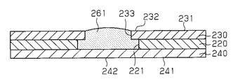
- the wiring board 210 is configured using a thick copper substrate. That is, the first copper plate 230 as the first metal plate is bonded to the upper surface of the insulating substrate 220 as the base material. A second copper plate 240 as a second metal plate is bonded to the lower surface of the insulating substrate 220. The first copper plate 230 is patterned into a desired shape to form a current path. Further, the second copper plate 240 is patterned into a desired shape to form a current path.
- a glass / epoxy resin substrate can be used for the insulating substrate 220.
- the thickness of the insulating substrate 220 is, for example, 400 ⁇ m
- the thickness of the first copper plate 230 is, for example, 500 ⁇ m
- the thickness of the second copper plate 240 is, for example, 500 ⁇ m.
- the conductor pattern made of the first copper plate 230 and the conductor pattern made of the second copper plate 240 are electrically connected in the following configuration.
- the wiring board 210 composed of a thick copper substrate includes a first copper plate 230 bonded to the surface (upper surface) of the insulating substrate 220 inside the base material through hole 221 that penetrates the insulating substrate 220, and an insulating substrate.
- a conductive path 250 is formed to conduct with the second copper plate 240 joined to the back surface (lower surface) of 220.
- the substrate through hole 221 has a circular shape.
- the conductive path 250 includes a first copper plate 230, a second copper plate 240, and solder 260 as a conductive material that electrically connects the first copper plate 230 and the second copper plate 240.
- the first copper plate 230 has a first extending portion 232.
- the first extending part 232 extends horizontally from the first joining part 231 joined to the insulating substrate 220 to one opening of the base material through hole 221.
- a first through hole 233 is formed at a portion corresponding to the central portion of the base material through hole 221 in the first extending portion 232.
- the first through hole 233 located at one opening of the base material through hole 221 has a circular shape and is smaller than the base material through hole 221.
- the second copper plate 240 has a second extending portion 242.
- the second extending portion 242 extends horizontally from the second joining portion 241 joined to the insulating substrate 220 to the other opening of the base material through hole 221.
- a second through hole 243 is formed in a portion corresponding to the central portion of the base material through hole 221 in the second extending portion 242.
- the second through hole 243 located at the other opening of the substrate through hole 221 has a circular shape.
- the second through hole 243 is smaller than the substrate through hole 221 and smaller than the first through hole 233.
- the second through hole 243 is provided at a portion facing the inside of the base material through hole 221 in the second copper plate 240.
- a metal plate (washer) 270 is disposed inside the base material through hole 221 in the insulating substrate 220.
- the metal plate 270 has a disk shape and engages with the substrate through hole 221.
- a third through hole 271 is formed at the center of the metal plate 270.
- the third through hole 271 has a circular shape.
- the third through hole 271 communicates with the first through hole 233 and the second through hole 243 and is smaller than the first through hole 233 and larger than the second through hole 243.
- the first through hole 233 and the third through hole 271 including the inside of the second through hole 243 are filled with solder 260 as a conductive material. It can be visually observed through the second through-hole 243 that the solder 260 is poured. That is, it can be assured that the solder 260 is poured.
- the first copper plate 230 is bonded to the surface of the insulating substrate 220 and the second copper plate 240 is bonded to the back surface of the insulating substrate 220.
- a metal plate 270 is disposed inside the substrate through hole 221, and solder 260 is filled in the through holes 233 and 271 including the inside of the through hole 243.
- the first copper plate 230 and the second copper plate 240 are electrically connected to each other by the solder 260.
- a current flows from the first copper plate 230 to the second copper plate 240. Specifically, a current flows from the first extending portion 232 to the second extending portion 242 through the solder 260. At this time, a large current (for example, 120 amperes) can be passed.
- a large current for example, 120 amperes
- a large current for example, 120 amperes
- a large current can be passed between the layers by devising the shapes of the copper plates 230 and 240 on both sides and soldering.
- a through hole 243 is formed in the second copper plate 240.
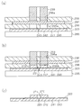
- a base material through hole 221 is formed in the insulating substrate 220 as the core material, and adhesives 222 and 223 are applied to both surfaces of the insulating substrate 220.
- the 2nd copper plate 240 in which the through-hole 243 which is located in the opening part of the base material through-hole 221 and smaller than the base-material through-hole 221 was formed in the back surface of the insulated substrate 220 is arrange
- a metal plate 270 that is in communication with the through hole 243 of the second copper plate 240 and has a through hole 271 larger than the through hole 243 is disposed inside the base material through hole 221. To do. When the metal plate (washer) 270 is disposed, the metal plate (washer) 270 need only be fitted. That is, the metal plate (washer) 270 is positioned at the opening of the core material (insulating base material 220).
- a first copper plate 230 having a through hole 233 communicating with the through hole 271 of the metal plate 270 is disposed on the surface of the insulating substrate 220.
- the laminated body of the insulating substrate 220 and the copper plates 230, 240 is heated and pressed using the upper and lower plates 280, 290 to be completely joined. That is, it joins with the adhesives 222 and 223 by applying heat and pressure with a laminating press.
- solder 260 as a conductive material is placed in the through hole 233 of the first copper plate 230 including the inside of the through hole 243 of the second copper plate 240 and the through hole 271 of the metal plate 270. Fill.
- solder paste is applied to the formation region of the through hole 233 on the surface of the first copper plate 230 and the periphery thereof. Then, by heating in the solder reflow furnace, the solder having fluidity flows downward from the application area of the solder paste, and the first copper plate including the inside of the through hole 243 of the second copper plate 240. The solder 260 is filled in the through holes 233 of the 230 and the through holes 271 of the metal plate 270.
- the through hole 243 is formed in the second copper plate 240, when the gas (air) confined in the space between the solder paste and the second copper plate 240 is warmed, the gas passes through the through hole 243. Can escape. By removing the gas, the solder wettability is stabilized. Further, by visually confirming the filling of the solder 260 into the through-hole 243 from the back surface (lower surface) of the wiring board 210, it can be seen that the solder 260 by reflow is sufficiently contained, and the quality of soldering can be determined. .
- the amount of solder can be saved by raising the metal plate (washer) 270.
- FIG. 16 the present embodiment using the metal plate (washer) 270 of FIG. 16 is compared with the comparative example not using the metal plate (washer) 270 of FIG.
- a metal plate (washer) 270 in FIGS. 16A, 16B, and 16C, a mask 265 is disposed and a solder paste 262 is applied to a desired region by a squeegee 266.
- the solder paste 262 adheres to the substrate-side surfaces S1, S2, S3, and S4 by the force of the flux, and the mask 265 is removed as shown in FIG. 16C.
- the solder paste 262 cleanly separates from the mask 265.
- FIG. 16B the case of FIG.
- the bonding surfaces of the solder paste 262 become S1 and S2, and the bonding surfaces decrease. For this reason, when the mask 265 is removed because the adhesive strength of the solder paste 262 is weak, the solder paste 262 may adhere to the mask 265 as shown in FIG.
- the solder paste adheres to the metal plate (washer) 270, so that it is possible to prevent the solder paste from adhering to the mask when the mask is removed.
- a through hole 243 is provided at a portion corresponding to the center of the base material through hole 221, and air is vented (degassed) using this through hole 243. By using it as a hole, the solder filling amount can be confirmed.
- the first extending portion 232 may not be provided.
- the second copper plate 240 has a second extending portion 242 extending from the joint portion 241 joined to the insulating substrate 220 to the opening of the base material through hole 221.
- a metal plate 270 in which a through hole 271 was formed was disposed inside the substrate through hole 221, and solder 260 as a conductive material was filled in the through hole 271 of the metal plate 270. Therefore, a large current can flow through the conductive path 250 connecting the front and back sides.
- the space filled with the solder 260 is narrowed by the metal plate 270 disposed in the space filled with the solder 260, the amount of the solder 260 to be filled can be reduced.
- a through hole 243 communicating with the through hole 271 of the metal plate 270 was formed in the extended portion 242 of the second copper plate 240. With this through hole 243, it is possible to perform at least one of degassing in the substrate through hole 221 (through hole 271) and inspection of the conductive path.
- the first copper plate 230 extends from the joint portion 231 joined to the insulating substrate 220 to the opening portion of the base material through hole 221, and forms a first through hole 233 smaller than the base material through hole 221.
- the extending portion 232 is provided.
- a metal plate 270 having a through hole 271 communicating with the through hole 233 of the first copper plate 230 is disposed inside the substrate through hole 221, and the through hole 233 of the first copper plate 230 and the through hole of the metal plate 270 are arranged. 271 is filled with solder 260 as a conductive material. Therefore, it is preferable for positioning the metal plate 270.
- the method for manufacturing a wiring board includes a second metal plate arranging step, a plate material arranging step, a first metal plate arranging step, and a solder filling step.
- the second copper plate 240 is formed on the back surface of the insulating substrate 220 and is located at the opening of the base material through hole 221 and has a through hole 243 smaller than the base material through hole 221.
- the metal plate 270 that communicates with the through hole 243 of the second copper plate 240 and has a larger through hole 271 than the through hole 243 of the second copper plate 240 is formed inside the base material through hole 221. Deploy.
- a first copper plate 230 in which a through hole 233 communicating with the through hole 271 of the metal plate 270 is formed on the surface of the insulating substrate 220 is arranged.
- the solder 260 as the conductive material is filled into the through holes 233 of the first copper plate 230 and the through holes 271 of the metal plate 270 including the inside of the through holes 243 of the second copper plate 240.
- the wiring board (10) can be obtained.
- a metal plate (washer) 270 in which a through hole 271 is formed may be bonded onto the second copper plate 240. More specifically, as shown in FIG. 18A, a second copper plate 240 is disposed on the stage 295, and an adhesive 223 is applied to the upper surface of the second copper plate 240. A die 296 is disposed on the second copper plate 240, and a die hole 296a is formed in the die 296. An unprocessed metal plate 297 is disposed on the die 296, a stripper 298 is disposed thereon, and a stripper hole 298 a is formed in the stripper 298. A punch 299 enters the stripper hole 298a.
- the punch 299 is lowered into the stripper hole 298a, and the metal plate 297 is punched out as shown in FIG. 18 (b) to form a metal plate (washer) 270 having a through hole 271. Further, the punch 299 is lowered into the die hole 296a, and the punched washer (the metal plate 270 having the through hole 271) is pressed against the adhesive 223.
- the punch 299 is raised and the die 296 is raised.
- the metal plate (washer) 270 in which the through hole 271 is formed is bonded onto the second copper plate 240.
- the insulating substrate 220 in which the base material through-hole 221 is formed is bonded onto the second copper plate 240.
- burrs are generated by punching by bonding the washer (the metal plate 270 having the through hole 271) to the upper surface of the second copper plate 240, but this bites into the adhesive 223. Therefore, the adhesive strength can be further improved.
- the adhesive 223 is preferably conductive.
- a metal plate 297 having a through hole 271 formed in advance may be used.
- the embodiment is not limited to the above, and may be embodied as follows, for example.
- the wiring boards 10 and 210 are configured using a thick copper substrate, the present invention is not limited to this, and for example, an aluminum plate or the like may be used as a metal plate instead of a copper plate.
- solder was used as the conductive material, other low melting point metals may be used.
- the bending angle of the first bent part 32, the bending angle of the second bent part 42 (slanted part 42a), the bending angle of the first bent part 35, the second bent part 45 ( The bending angle of the inclined portion 45a) is not limited.
- the number of through holes formed in the second metal plate is not limited. For example, about 1 to 4 pieces may be prepared. In the case of a plurality of through holes, the through holes are preferably arranged at equal angular intervals.
- the metal plate on which the bent portion is formed is extended from the joint portion joined to the base material, and the metal plate on which the bent portion is not formed is provided on the base material. It is good also as a structure which is not extended from the junction part joined.
- wiring board 220 ... insulating substrate, 221 ... Substrate through hole, 230 ... first copper plate, 231 ... first joint, 232 ... first extension, 233 ... first through hole, 240 ... second copper plate, 241 ... second 242 ... second extending portion, 243 ... second through hole, 250 ... conductive path, 260 ... solder, 270 ... metal plate, 271 ... 3 of the through-hole.
Abstract
Description
本発明の第3の態様に係る配線板の製造方法において、配線板は、表面と裏面と側面とを有する基材と、前記表面に接合される第一の金属板と、前記裏面に接合される第二の金属板と、前記第一の金属板と第二の金属板との間を導電するように構成される導電路であって、同導電路は前記基材に形成された基材貫通孔の内壁面によって画定される内部空間に設けられ、前記導電路は、前記第一の金属板と、前記第二の金属板と、前記第一の金属板と前記第二の金属板とを電気的に接続する導電材とを含む、前記導電路と、を備える。前記第一の金属板および前記第二の金属板の少なくとも一方は、前記基材に接合される接合部と、前記内壁面を覆うように前記接合部から折れ曲がるように延びる折曲り部とを有する。前記配線板の製造方法は、前記表面に前記第一の金属板を接合する工程と、前記裏面に前記基材貫通孔の一方の開口端を塞ぐように前記第二の金属板を接合する工程と、前記第一の金属板の表面において前記基材貫通孔の他方の開口端に対応する部位にはんだペーストを塗布する工程と、前記第二の金属板において前記内部空間に臨む部位に貫通孔を形成する工程と、前記はんだペーストをリフローして前記第二の金属板の貫通孔からガスを抜きながら当該貫通孔と前記折曲り部の内側部とによって形成された空間に導電材としてのはんだを充填する工程と、を備える。
以下、本発明を具体化した第1の実施形態を図面に従って説明する。
次に、第2の実施形態を、第1の実施形態との相違点を中心に説明する。
次に、第3の実施形態を、第1の実施形態との相違点を中心に説明する。
次に、第4の実施形態を、図11~図14を用いて説明する。
Claims (11)
- 表面と裏面と側面とを有する基材と、
前記表面に接合される第一の金属板と、
前記裏面に接合される第二の金属板と、
前記第一の金属板と第二の金属板との間を導電するように構成される導電路であって、同導電路は前記基材に形成された基材貫通孔の内壁面によって画定される内部空間または前記基材の側面より外側の外部空間に設けられ、前記導電路は、前記第一の金属板と、前記第二の金属板と、前記第一の金属板と前記第二の金属板とを電気的に接続する導電材とを含む、前記導電路と、を備え、
前記第一の金属板および前記第二の金属板の少なくとも一方は、前記基材に接合される接合部と、前記内壁面または前記側面を覆うように前記接合部から折れ曲がるように延びる折曲り部とを有し、
前記折曲り部の内側部に前記導電材が充填される、配線板。 - 前記第一の金属板は、前記接合部としての第一の接合部と前記折曲り部としての第一の折曲り部とを有し、同第一の折曲り部は前記裏面に向かって折れ曲がり、
前記第二の金属板は、前記接合部としての第二の接合部と前記折曲り部としての第二の折曲り部とを有し、同第二の折曲り部は前記第一の折曲り部と共に前記内壁面または前記側面を覆うように前記表面に向かって折れ曲がり、
前記導電材は前記第一の折曲り部と前記第二の折曲り部との間に充填される、請求項1に記載の配線板。 - 前記第二の金属板は、前記内部空間または前記外部空間に臨む部位に貫通孔を有する、請求項1または2に記載の配線板。
- 前記導電路は前記内部空間に設けられ、
前記第一の折曲り部は、前記表面に開口する前記基材貫通孔の開口端から前記内部空間に向かって折れ曲がるとともに、前記基材貫通孔の中心部に対応する部位に貫通孔を有しており、
前記第二の折曲り部は、前記裏面に開口する前記基材貫通孔の開口端から前記内部空間に向かって折れ曲がるとともに、前記第一の折曲り部の貫通孔内に挿入されている、請求項2または3に記載の配線板。 - 前記第二の金属板に形成されている前記貫通孔は、断面円形の前記基材貫通孔の中心軸線を中心とした円周上に複数設けられている、請求項3に記載の配線板。
- 前記第二の金属板に形成されている前記複数の貫通孔は等角度間隔をもって配置されている、請求項5に記載の配線板。
- 表面と裏面と基材貫通孔とを有する基材と、
前記表面に接合される第一の金属板と、
前記裏面に接合される第二の金属板と、
前記第一の金属板と第二の金属板との間を導電するように前記基材貫通孔の内部空間に設けられる導電路であって、前記導電路は、前記第一の金属板と、前記第二の金属板と、前記第一の金属板と前記第二の金属板とを電気的に接続する導電材とを含む、前記導電路と、を備え、
前記第二の金属板は、前記基材に接合される接合部と同接合部から前記基材貫通孔の開口部に延びる延設部とを有し、
前記内部空間に、前記基材貫通孔と連通する貫通孔を有する板材が配置され、
前記板材の貫通孔の内部に前記導電材が充填される、配線板。 - 前記延設部は、前記板材の貫通孔と連通する貫通孔を有する、請求項7に記載の配線板。
- 前記第一の金属板は、前記基材に接合される接合部と同接合部から前記基材貫通孔の開口部に延びる延設部とを有し、同延設部は前記基材貫通孔よりも小さい貫通孔を有しており、
前記板材の前記貫通孔は前記第一の金属板の貫通孔と連通し、前記第一の金属板の貫通孔および前記板材の貫通孔の内部に前記導電材が充填される、請求項7または8に記載の配線板。 - 表面と裏面と側面とを有する基材と、
前記表面に接合される第一の金属板と、
前記裏面に接合される第二の金属板と、
前記第一の金属板と第二の金属板との間を導電するように構成される導電路であって、同導電路は前記基材に形成された基材貫通孔の内壁面によって画定される内部空間に設けられ、前記導電路は、前記第一の金属板と、前記第二の金属板と、前記第一の金属板と前記第二の金属板とを電気的に接続する導電材とを含む、前記導電路と、を備え、
前記第一の金属板および前記第二の金属板の少なくとも一方は、前記基材に接合される接合部と、前記内壁面を覆うように前記接合部から折れ曲がるように延びる折曲り部とを有する、
配線板の製造方法であって、
前記表面に前記第一の金属板を接合する工程と、
前記裏面に前記基材貫通孔の一方の開口端を塞ぐように前記第二の金属板を接合する工程と、
前記第一の金属板の表面において前記基材貫通孔の他方の開口端に対応する部位にはんだペーストを塗布する工程と、
前記第二の金属板において前記内部空間に臨む部位に貫通孔を形成する工程と、
前記はんだペーストをリフローして前記第二の金属板の貫通孔からガスを抜きながら当該貫通孔と前記折曲り部の内側部とによって形成された空間に導電材としてのはんだを充填する工程と、
を備える、配線板の製造方法。 - 表面と裏面と側面とを有する基材と、
前記表面に接合される第一の金属板と、
前記裏面に接合される第二の金属板と、
前記第一の金属板と第二の金属板との間を導電するように構成される導電路であって、同導電路は前記基材に形成された基材貫通孔の内壁面によって画定される内部空間に設けられ、前記導電路は、前記第一の金属板と、前記第二の金属板と、前記第一の金属板と前記第二の金属板とを電気的に接続する導電材とを含む、前記導電路と、
を備える配線板の製造方法であって、
前記裏面に貫通孔を有する前記第二の金属板を配置する工程であって、前記第二の金属板の貫通孔は、前記基材貫通孔と連通するとともに前記基材貫通孔よりも小さい開口面積を有する、前記工程と、
前記基材貫通孔に貫通孔を有する板材を配置する工程であって、前記板材の貫通孔は、前記第二の金属板の貫通孔と連通するとともに前記第二の金属板の貫通孔よりも大きい開口面積を有する、前記工程と、
前記表面に貫通孔を有する前記第一の金属板を配置する工程であって、前記第一の金属板の貫通孔は前記板材の貫通孔と連通する、前記工程と、
前記第二の金属板の貫通孔と前記第一の金属板の貫通孔と前記板材の貫通孔とによって形成された空間に導電材としてのはんだを充填する工程と、
を備える、配線板の製造方法。
Priority Applications (5)
| Application Number | Priority Date | Filing Date | Title |
|---|---|---|---|
| EP12789574.6A EP2717658B1 (en) | 2011-05-26 | 2012-05-23 | Wiring board and method for manufacturing wiring board |
| KR1020137030367A KR20130140889A (ko) | 2011-05-26 | 2012-05-23 | 배선판 및 배선판의 제조 방법 |
| JP2013516414A JP5742936B2 (ja) | 2011-05-26 | 2012-05-23 | 配線板および配線板の製造方法 |
| US14/118,636 US9332638B2 (en) | 2011-05-26 | 2012-05-23 | Wiring board and method for manufacturing wiring board |
| CN201280024409.6A CN103563495B (zh) | 2011-05-26 | 2012-05-23 | 布线板以及布线板的制造方法 |
Applications Claiming Priority (2)
| Application Number | Priority Date | Filing Date | Title |
|---|---|---|---|
| JP2011118332 | 2011-05-26 | ||
| JP2011-118332 | 2011-05-26 |
Publications (1)
| Publication Number | Publication Date |
|---|---|
| WO2012161218A1 true WO2012161218A1 (ja) | 2012-11-29 |
Family
ID=47217294
Family Applications (1)
| Application Number | Title | Priority Date | Filing Date |
|---|---|---|---|
| PCT/JP2012/063186 WO2012161218A1 (ja) | 2011-05-26 | 2012-05-23 | 配線板および配線板の製造方法 |
Country Status (7)
| Country | Link |
|---|---|
| US (1) | US9332638B2 (ja) |
| EP (1) | EP2717658B1 (ja) |
| JP (1) | JP5742936B2 (ja) |
| KR (1) | KR20130140889A (ja) |
| CN (1) | CN103563495B (ja) |
| TW (1) | TWI451817B (ja) |
| WO (1) | WO2012161218A1 (ja) |
Cited By (3)
| Publication number | Priority date | Publication date | Assignee | Title |
|---|---|---|---|---|
| WO2015093249A1 (ja) * | 2013-12-19 | 2015-06-25 | 株式会社 豊田自動織機 | 配線板 |
| WO2015093250A1 (ja) * | 2013-12-19 | 2015-06-25 | 株式会社 豊田自動織機 | 配線板の製造方法 |
| WO2015125951A1 (ja) * | 2014-02-24 | 2015-08-27 | 株式会社村田製作所 | 多層基板の製造方法および多層基板 |
Families Citing this family (1)
| Publication number | Priority date | Publication date | Assignee | Title |
|---|---|---|---|---|
| JP2019212747A (ja) * | 2018-06-05 | 2019-12-12 | 日本ケミコン株式会社 | バスバー積層体及びそれを備える電子部品実装モジュール、バスバー積層体の製造方法 |
Citations (5)
| Publication number | Priority date | Publication date | Assignee | Title |
|---|---|---|---|---|
| JPS54156167A (en) * | 1978-05-31 | 1979-12-08 | Matsushita Electric Ind Co Ltd | Method of producing double side printed circuit board |
| JPS5511174Y2 (ja) * | 1972-11-29 | 1980-03-11 | ||
| JPH10126013A (ja) * | 1996-10-21 | 1998-05-15 | Nec Corp | 配線基板 |
| JP2001284800A (ja) * | 2000-02-18 | 2001-10-12 | Eupec Europaeische Ges Fuer Leistungshalbleiter Mbh & Co Kg | はんだによるスルーコンタクトを有する出力半導体モジュールのための基板及び該基板の製作法 |
| JP2010267649A (ja) | 2009-05-12 | 2010-11-25 | Tibc:Kk | プリント配線板 |
Family Cites Families (21)
| Publication number | Priority date | Publication date | Assignee | Title |
|---|---|---|---|---|
| US4064357A (en) * | 1975-12-02 | 1977-12-20 | Teledyne Electro-Mechanisms | Interconnected printed circuits and method of connecting them |
| FR2439322A1 (fr) | 1978-10-19 | 1980-05-16 | Cii Honeywell Bull | Procede et dispositif de liaison de deux elements et outil pour l'execution du procede |
| CA1100319A (en) | 1979-05-10 | 1981-05-05 | Eugene E. Young | Oil return system and method |
| GB2085233A (en) | 1980-08-19 | 1982-04-21 | Renishaw Electrical Ltd | Electric circuit board assembly |
| US4769269A (en) * | 1983-12-05 | 1988-09-06 | E. I. Du Pont De Nemours And Company | Article containing conductive through-holes |
| JPH0437087A (ja) | 1990-05-31 | 1992-02-07 | Toshiba Corp | 印刷配線板装置並びにその装置に用いるハトメ及びその取付け方法 |
| DE59309575D1 (de) | 1992-06-15 | 1999-06-17 | Heinze Dyconex Patente | Verfahren zur herstellung von leiterplatten unter verwendung eines halbzeuges mit extrem dichter verdrahtung für die signalführung |
| ATE137079T1 (de) | 1992-06-15 | 1996-05-15 | Heinze Dyconex Patente | Verfahren zur herstellung von nachträglich konditionierbaren kontaktstellen an schaltungsträgern und schaltungsträger mit solchen kontaktstellen |
| EP0575292B1 (de) * | 1992-06-15 | 1996-03-13 | Dyconex Patente Ag | Verfahren zur Herstellung von Substraten mit Durchführungen |
| US5433819A (en) * | 1993-05-26 | 1995-07-18 | Pressac, Inc. | Method of making circuit boards |
| TW512467B (en) * | 1999-10-12 | 2002-12-01 | North Kk | Wiring circuit substrate and manufacturing method therefor |
| JP2002185120A (ja) | 2000-12-19 | 2002-06-28 | Toshiba Corp | 部品実装基板およびその製造方法 |
| JP2005072095A (ja) * | 2003-08-20 | 2005-03-17 | Alps Electric Co Ltd | 電子回路ユニットおよびその製造方法 |
| JP2006093577A (ja) | 2004-09-27 | 2006-04-06 | Hitachi Cable Ltd | 半導体装置用転写フィルム基板及びその製造方法並びにそれを用いた半導体装置 |
| JP2006303126A (ja) * | 2005-04-20 | 2006-11-02 | Oki Electric Ind Co Ltd | プリント配線基板の製造方法 |
| KR101046890B1 (ko) * | 2005-06-15 | 2011-07-06 | 이비덴 가부시키가이샤 | 다층 프린트 배선판 |
| JP2008021637A (ja) * | 2006-06-12 | 2008-01-31 | Fujikura Ltd | ソケットとその製造方法及び半導体装置 |
| JP5629580B2 (ja) * | 2007-09-28 | 2014-11-19 | テッセラ,インコーポレイテッド | 二重ポスト付きフリップチップ相互接続 |
| US8324723B2 (en) * | 2008-03-25 | 2012-12-04 | Bridge Semiconductor Corporation | Semiconductor chip assembly with bump/base heat spreader and dual-angle cavity in bump |
| ES2369840T3 (es) * | 2009-03-30 | 2011-12-07 | Eberspächer Catem Gmbh & Co. Kg | Dispositivo calefactor eléctrico para un automóvil. |
| TWI400025B (zh) * | 2009-12-29 | 2013-06-21 | Subtron Technology Co Ltd | 線路基板及其製作方法 |
-
2012
- 2012-05-22 TW TW101118142A patent/TWI451817B/zh not_active IP Right Cessation
- 2012-05-23 JP JP2013516414A patent/JP5742936B2/ja not_active Expired - Fee Related
- 2012-05-23 EP EP12789574.6A patent/EP2717658B1/en not_active Not-in-force
- 2012-05-23 US US14/118,636 patent/US9332638B2/en active Active
- 2012-05-23 KR KR1020137030367A patent/KR20130140889A/ko not_active Application Discontinuation
- 2012-05-23 WO PCT/JP2012/063186 patent/WO2012161218A1/ja active Application Filing
- 2012-05-23 CN CN201280024409.6A patent/CN103563495B/zh not_active Expired - Fee Related
Patent Citations (5)
| Publication number | Priority date | Publication date | Assignee | Title |
|---|---|---|---|---|
| JPS5511174Y2 (ja) * | 1972-11-29 | 1980-03-11 | ||
| JPS54156167A (en) * | 1978-05-31 | 1979-12-08 | Matsushita Electric Ind Co Ltd | Method of producing double side printed circuit board |
| JPH10126013A (ja) * | 1996-10-21 | 1998-05-15 | Nec Corp | 配線基板 |
| JP2001284800A (ja) * | 2000-02-18 | 2001-10-12 | Eupec Europaeische Ges Fuer Leistungshalbleiter Mbh & Co Kg | はんだによるスルーコンタクトを有する出力半導体モジュールのための基板及び該基板の製作法 |
| JP2010267649A (ja) | 2009-05-12 | 2010-11-25 | Tibc:Kk | プリント配線板 |
Non-Patent Citations (1)
| Title |
|---|
| See also references of EP2717658A4 |
Cited By (5)
| Publication number | Priority date | Publication date | Assignee | Title |
|---|---|---|---|---|
| WO2015093249A1 (ja) * | 2013-12-19 | 2015-06-25 | 株式会社 豊田自動織機 | 配線板 |
| WO2015093250A1 (ja) * | 2013-12-19 | 2015-06-25 | 株式会社 豊田自動織機 | 配線板の製造方法 |
| JP2015119097A (ja) * | 2013-12-19 | 2015-06-25 | 株式会社豊田自動織機 | 配線板 |
| JP2015119098A (ja) * | 2013-12-19 | 2015-06-25 | 株式会社豊田自動織機 | 配線板及び配線板の製造方法 |
| WO2015125951A1 (ja) * | 2014-02-24 | 2015-08-27 | 株式会社村田製作所 | 多層基板の製造方法および多層基板 |
Also Published As
| Publication number | Publication date |
|---|---|
| TW201301965A (zh) | 2013-01-01 |
| TWI451817B (zh) | 2014-09-01 |
| EP2717658A4 (en) | 2015-08-12 |
| EP2717658A1 (en) | 2014-04-09 |
| JP5742936B2 (ja) | 2015-07-01 |
| EP2717658B1 (en) | 2017-10-18 |
| US20140151106A1 (en) | 2014-06-05 |
| KR20130140889A (ko) | 2013-12-24 |
| CN103563495A (zh) | 2014-02-05 |
| JPWO2012161218A1 (ja) | 2014-07-31 |
| US9332638B2 (en) | 2016-05-03 |
| CN103563495B (zh) | 2016-10-12 |
Similar Documents
| Publication | Publication Date | Title |
|---|---|---|
| US8069558B2 (en) | Method for manufacturing substrate having built-in components | |
| JP5931799B2 (ja) | 層間接続基板およびその製造方法 | |
| TW200810626A (en) | Method for manufacturing multilayer wiring board | |
| JP2007073866A (ja) | 部品内蔵配線板 | |
| JP2007335701A (ja) | 積層基板の製造方法 | |
| JP2007273654A (ja) | フレキシブル回路基板、フレキシブル回路基板の製造方法および電子機器 | |
| JP5742936B2 (ja) | 配線板および配線板の製造方法 | |
| KR20110077042A (ko) | 인쇄회로기판조립체의 제조방법 | |
| WO2013005576A1 (ja) | 配線板 | |
| JP5958768B2 (ja) | 回路構成体 | |
| JP2019047127A (ja) | 樹脂多層基板 | |
| JP2013073989A (ja) | 表面実装型受動素子部品、部品キャリアテープ、部品内蔵配線板 | |
| JP2010098021A (ja) | 部品内蔵配線基板および部品内蔵配線基板の製造方法 | |
| CN213126630U (zh) | 树脂基板以及电子设备 | |
| JP2014157857A (ja) | 部品内蔵樹脂多層基板およびその製造方法 | |
| WO2013137401A1 (ja) | 電子部品搭載用基板の製造方法及び電子部品搭載用基板 | |
| JP4856567B2 (ja) | プリント配線板及び電子部品実装基板 | |
| JP2005039136A (ja) | 回路基板および回路基板の接続方法 | |
| JP5003528B2 (ja) | 電子部品モジュールの製造方法 | |
| JP2006269466A (ja) | プリント回路基板およびその製造方法 | |
| JP5428539B2 (ja) | 配線基板の製造方法 | |
| JP4556723B2 (ja) | 接合方法および配線板の製造方法 | |
| JP5807670B2 (ja) | 配線板 | |
| CN118042733A (en) | Electronic assembly method, circuit board assembly and communication equipment | |
| JP2006324282A (ja) | 多層プリント配線板及びその製造方法 |
Legal Events
| Date | Code | Title | Description |
|---|---|---|---|
| 121 | Ep: the epo has been informed by wipo that ep was designated in this application |
Ref document number: 12789574 Country of ref document: EP Kind code of ref document: A1 |
|
| ENP | Entry into the national phase |
Ref document number: 2013516414 Country of ref document: JP Kind code of ref document: A |
|
| ENP | Entry into the national phase |
Ref document number: 20137030367 Country of ref document: KR Kind code of ref document: A |
|
| NENP | Non-entry into the national phase |
Ref country code: DE |
|
| REEP | Request for entry into the european phase |
Ref document number: 2012789574 Country of ref document: EP |
|
| WWE | Wipo information: entry into national phase |
Ref document number: 14118636 Country of ref document: US |