WO2012147759A1 - 有機el素子用の光取出し透明基板及びそれを用いた有機el素子 - Google Patents
有機el素子用の光取出し透明基板及びそれを用いた有機el素子 Download PDFInfo
- Publication number
- WO2012147759A1 WO2012147759A1 PCT/JP2012/061022 JP2012061022W WO2012147759A1 WO 2012147759 A1 WO2012147759 A1 WO 2012147759A1 JP 2012061022 W JP2012061022 W JP 2012061022W WO 2012147759 A1 WO2012147759 A1 WO 2012147759A1
- Authority
- WO
- WIPO (PCT)
- Prior art keywords
- layer
- organic
- unevenness
- concavo
- uneven
- Prior art date
Links
Images


Classifications
-
- H—ELECTRICITY
- H10—SEMICONDUCTOR DEVICES; ELECTRIC SOLID-STATE DEVICES NOT OTHERWISE PROVIDED FOR
- H10K—ORGANIC ELECTRIC SOLID-STATE DEVICES
- H10K50/00—Organic light-emitting devices
- H10K50/80—Constructional details
- H10K50/85—Arrangements for extracting light from the devices
- H10K50/858—Arrangements for extracting light from the devices comprising refractive means, e.g. lenses
-
- F—MECHANICAL ENGINEERING; LIGHTING; HEATING; WEAPONS; BLASTING
- F21—LIGHTING
- F21V—FUNCTIONAL FEATURES OR DETAILS OF LIGHTING DEVICES OR SYSTEMS THEREOF; STRUCTURAL COMBINATIONS OF LIGHTING DEVICES WITH OTHER ARTICLES, NOT OTHERWISE PROVIDED FOR
- F21V13/00—Producing particular characteristics or distribution of the light emitted by means of a combination of elements specified in two or more of main groups F21V1/00 - F21V11/00
- F21V13/02—Combinations of only two kinds of elements
- F21V13/10—Combinations of only two kinds of elements the elements being reflectors and screens
-
- H—ELECTRICITY
- H10—SEMICONDUCTOR DEVICES; ELECTRIC SOLID-STATE DEVICES NOT OTHERWISE PROVIDED FOR
- H10K—ORGANIC ELECTRIC SOLID-STATE DEVICES
- H10K50/00—Organic light-emitting devices
- H10K50/80—Constructional details
-
- H—ELECTRICITY
- H10—SEMICONDUCTOR DEVICES; ELECTRIC SOLID-STATE DEVICES NOT OTHERWISE PROVIDED FOR
- H10K—ORGANIC ELECTRIC SOLID-STATE DEVICES
- H10K50/00—Organic light-emitting devices
- H10K50/80—Constructional details
- H10K50/85—Arrangements for extracting light from the devices
-
- B—PERFORMING OPERATIONS; TRANSPORTING
- B82—NANOTECHNOLOGY
- B82Y—SPECIFIC USES OR APPLICATIONS OF NANOSTRUCTURES; MEASUREMENT OR ANALYSIS OF NANOSTRUCTURES; MANUFACTURE OR TREATMENT OF NANOSTRUCTURES
- B82Y20/00—Nanooptics, e.g. quantum optics or photonic crystals
-
- Y—GENERAL TAGGING OF NEW TECHNOLOGICAL DEVELOPMENTS; GENERAL TAGGING OF CROSS-SECTIONAL TECHNOLOGIES SPANNING OVER SEVERAL SECTIONS OF THE IPC; TECHNICAL SUBJECTS COVERED BY FORMER USPC CROSS-REFERENCE ART COLLECTIONS [XRACs] AND DIGESTS
- Y10—TECHNICAL SUBJECTS COVERED BY FORMER USPC
- Y10S—TECHNICAL SUBJECTS COVERED BY FORMER USPC CROSS-REFERENCE ART COLLECTIONS [XRACs] AND DIGESTS
- Y10S977/00—Nanotechnology
- Y10S977/70—Nanostructure
- Y10S977/832—Nanostructure having specified property, e.g. lattice-constant, thermal expansion coefficient
- Y10S977/834—Optical properties of nanomaterial, e.g. specified transparency, opacity, or index of refraction
Definitions
- the present invention relates to a light extraction transparent substrate for an organic EL element and an organic EL element using the same.
- Organic electroluminescence elements are used as self-luminous elements as video display devices such as displays and as surface light sources.
- Such an organic EL element is generally produced by sequentially laminating a transparent electrode as an anode, an organic layer, and a metal electrode as a cathode on a transparent support substrate such as a glass substrate or a transparent plastic film. It is what is done. In this way, the electrons applied from the cathode and the holes supplied from the anode are recombined in the organic layer due to the voltage applied between the transparent electrode and the metal electrode, and excitons generated accordingly.
- EL emits light when it shifts from the excited state to the ground state. The light emitted from the EL is transmitted through the transparent electrode and taken out from the transparent support substrate side.
- the organic EL element described in Patent Document 1 and the organic EL element using the microlens described in Non-Patent Document 1 have sufficiently high light extraction efficiency.
- the appearance of an organic EL element in which the change in angle dependency and chromaticity is sufficiently reduced is desired.
- the present invention has been made in view of the above-described problems of the prior art, and can sufficiently improve the light extraction efficiency of the organic EL element, and can sufficiently reduce the change in chromaticity. At the same time, it is an object to provide a light extraction transparent substrate for an organic EL element capable of sufficiently reducing the angle dependency of luminance, and an organic EL element using the same.
- the transparent support substrate is provided with a diffraction grating composed of a first concavo-convex layer having a first concavo-convex formed on the surface side to be a light incident surface of the EL element, and when used in an organic EL element.
- a microlens composed of a second concavo-convex layer having a second concavo-convex formed on the surface side to be a light exit surface of the organic EL element is provided.
- the light extraction transparent substrate for an organic EL element of the present invention is a light extraction transparent substrate for an organic EL element comprising a transparent support substrate used by being disposed on the light emission surface side of the organic EL element,
- the transparent support substrate is provided with a diffraction grating composed of a first concavo-convex layer having a first concavo-convex layer formed on the surface side to be a light incident surface of the organic EL element
- the surface of the transparent support substrate, which should be the light emission surface of the organic EL element is provided with a microlens composed of a second uneven layer having a second unevenness formed on the surface,
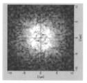
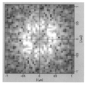
- Each of the first and second uneven shapes was subjected to two-dimensional fast Fourier transform processing on the unevenness analysis image obtained by analyzing the uneven shape with an atomic force microscope to obtain a Fourier transform image.
- the Fourier transform image has a shape showing a circular or annular pattern whose
- the circular or annular pattern of the Fourier transform image of the first uneven shape has a wave number having an absolute value of 10 ⁇ m ⁇ 1 or less. Exists in the inner area, and The circular or annular pattern of the Fourier transform image relating to the shape of the second unevenness is preferably present in a region where the absolute value of the wave number is in the range of 1 ⁇ m ⁇ 1 or less.
- the average height of the first unevenness is 30 to 100 nm and the average pitch is 10 to 700 nm. It is preferable that the average height is 400 to 1000 nm and the average pitch is 2 to 10 ⁇ m.
- the average value and the median value of the depth distribution of the first unevenness are represented by the following inequality (1): 0.95 ⁇ Y ⁇ M ⁇ 1.05 ⁇ Y (1)
- M represents the median value of the depth distribution of the unevenness.
- the kurtosis of the first unevenness is preferably a value of ⁇ 1.2 or more, and is in a range of ⁇ 1.2 to 1.2. A value within the range is more preferable.
- the light extraction transparent substrate for the organic EL element of the present invention light is incident on the light extraction transparent substrate from the first uneven layer side and light is emitted from the second uneven layer side.
- the following inequality (2) ⁇ (y ( ⁇ ) ⁇ y 0 ( ⁇ )) 2 ⁇ 0.05 (2) [In the formula, ⁇ represents a measurement angle of 33 points when changing from ⁇ 80 ° to 80 ° by 5 °, and y ( ⁇ ) represents an emission spectrum intensity measurement value at an angle ⁇ of 0 °.
- y 0 ( ⁇ ) represents a theoretical value of an emission spectrum intensity at an angle ⁇ obtained from a radiation pattern based on Lambert's law at an angle of 0 ° obtained from the radiation pattern. The value normalized by the theoretical value of the emission spectrum intensity is shown. ] It is preferable to satisfy the conditions shown in
- the second uneven layer is laminated on the transparent support substrate via an adhesive layer and / or an adhesive layer.
- a protective layer is laminated on the surface on which the uneven shape of the second uneven layer is formed.
- the organic EL device of the present invention includes a transparent support substrate, A diffraction grating comprising a first concavo-convex layer disposed on one surface side of the transparent support substrate and having a first concavo-convex formed on the surface; A microlens composed of a second concavo-convex layer disposed on the other surface side of the transparent support substrate and having a second concavo-convex formed on the surface; and A transparent electrode, an organic layer, and a metal electrode are sequentially stacked on the first uneven layer so that the shape of the first unevenness formed on the surface of the first uneven layer is maintained. And A component formed by the transparent support substrate, the diffraction grating, and the microlens is composed of the light extraction transparent substrate for the organic EL element of the present invention.
- the light extraction efficiency of the organic EL element can be sufficiently improved, the change in chromaticity can be sufficiently reduced, and the angle dependency of luminance can be sufficiently reduced. It is possible to provide a light extraction transparent substrate for an organic EL element that can be used, and an organic EL element using the same.
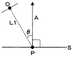
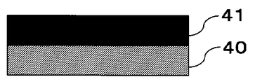
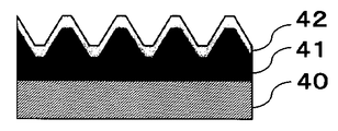
- FIG. 3 is a cross-sectional view schematically showing a state in which irregularities are formed on the surface of the diffraction grating 11 by removing the master for forming the diffraction grating. It is a conceptual diagram which shows notionally the measurement angle (theta).
- the light extraction transparent substrate for an organic EL element of the present invention is a light extraction transparent substrate for an organic EL element comprising a transparent support substrate used by being disposed on the light emission surface side of the organic EL element,
- the transparent support substrate is provided with a diffraction grating composed of a first concavo-convex layer having a first concavo-convex layer formed on the surface side to be a light incident surface of the organic EL element
- the surface of the transparent support substrate, which should be the light emission surface of the organic EL element is provided with a microlens composed of a second uneven layer having a second unevenness formed on the surface,
- Each of the first and second uneven shapes was subjected to two-dimensional fast Fourier transform processing on the unevenness analysis image obtained by analyzing the uneven shape with an atomic force microscope to obtain a Fourier transform image.
- the Fourier transform image has a shape showing
- FIG. 1 is a cross-sectional view schematically showing a preferred embodiment of a light extraction transparent substrate for an organic EL device of the present invention.
- a light extraction transparent substrate 1 shown in FIG. 1 includes a transparent support substrate 10, a diffraction grating 11, and a microlens 12.
- the arrow L in FIG. 1 is an arrow which shows notionally the direction which the light from the inside advances when the light extraction transparent substrate is used for an organic EL element, when the organic EL element is issued. .
- the well-known transparent substrate which can be used for an organic EL element can be utilized suitably, for example, a board
- the thickness of the transparent support substrate 10 is preferably in the range of 1 to 500 ⁇ m.
- the diffraction grating 11 is a layer (first concavo-convex layer) having a first concavo-convex formed on the surface.
- a material (diffraction grating forming material) for forming such a diffraction grating (first concavo-convex layer) for example, epoxy resin, acrylic resin, urethane resin, melamine resin, urea resin, polyester resin, phenol resin, Resin material (material made of curable resin) such as cross-linked liquid crystal resin, or transparent inorganic layer forming material (for example, when forming a transparent inorganic layer by forming an uneven layer by sol-gel method, metal such as metal alkoxide And a sol solution containing the material).
- the diffraction grating 11 may be a cured resin layer obtained by curing the resin material or an inorganic layer formed using a transparent inorganic layer forming material. From the viewpoint of obtaining a layer having characteristics such as high heat resistance and mechanical strength, an inorganic layer is preferable.
- the thickness of the first uneven layer is preferably in the range of 0.01 to 500 ⁇ m (more preferably 0.5 to 500 ⁇ m).
- the thickness of the first concavo-convex layer is less than the lower limit, the height of the concavo-convex formed on the surface of the first concavo-convex layer tends to be insufficient.
- the thickness exceeds the upper limit the diffraction grating forming material generated during curing The influence of volume change of (for example, resin) tends to be large and the uneven shape cannot be formed satisfactorily.
- the unevenness analysis image obtained by analyzing the shape of the first unevenness formed on the surface of the first unevenness layer using an atomic force microscope is subjected to a two-dimensional fast Fourier transform process.
- the Fourier transform image needs to show a circular or annular pattern substantially centered at the origin where the absolute value of the wave number is 0 ⁇ m ⁇ 1 .
- the circular or annular pattern of the Fourier transform image having the first uneven shape preferably exists in a region where the absolute value of the wave number is in the range of 10 ⁇ m ⁇ 1 or less.
- the Fourier transform image shows the above-mentioned conditions, by forming a concavo-convex shape on the surface of the concavo-convex layer, the wavelength dependence and directivity of the diffraction grating tend to be reduced at a higher level.
- the pattern of such a Fourier transform image is more preferably an annular shape from the viewpoint that a higher effect can be obtained in terms of wavelength dependency and directivity.
- the circular or annular pattern of the Fourier transform image has an absolute value of wave number of 1.25 to 10 ⁇ m ⁇ 1. More preferably, it exists in a region within the range of (more preferably from 1.25 to 5 ⁇ m ⁇ 1 ).
- the “circular or annular pattern of the Fourier transform image” referred to in the present invention is a pattern observed when bright spots are gathered in the Fourier transform image. Therefore, the “circular shape” in the present invention means that a pattern in which bright spots are gathered appears to be a substantially circular shape, and includes those in which a part of the outer shape appears to be convex or concave. It is a concept, and “annular” means that the pattern of bright spots appears to be almost circular, and the outer circle and inner circle appear to be almost circular. And a part of the outer circle of the ring or a part of the outer shape of the inner circle that appears to be convex or concave.
- a circular or annular pattern has an absolute value of wave number of 10 ⁇ m ⁇ 1 or less (preferably 1.25 to 10 ⁇ m ⁇ 1 , more preferably 1.25 to 5 ⁇ m ⁇ 1 ).
- “Is present in the region” means that 30% or more (more preferably 50% or more, still more preferably 80% or more, particularly preferably 90% or more) of the luminescent spots constituting the Fourier transform image. Is in a region where the absolute value of the wave number falls within the range of 10 ⁇ m ⁇ 1 or less (preferably 1.25 to 10 ⁇ m ⁇ 1 , more preferably 1.25 to 5 ⁇ m ⁇ 1 ).
- the Fourier transform image is obtained by analyzing the shape of the unevenness formed on the surface of the uneven layer using an atomic force microscope to obtain an unevenness analysis image, and then performing a two-dimensional fast Fourier transform process on the unevenness analysis image. It is obtained by applying.
- the unevenness analysis image is analyzed using an atomic force microscope under the following analysis conditions: Measuring method: Cantilever intermittent contact method Cantilever material: Silicon cantilever lever width: 40 ⁇ m Cantilever tip tip diameter: 10 nm Can be obtained by analysis.
- a commercially available one can be used as appropriate, and for example, a scanning probe microscope “Nonavi II station / E-sweep” with an environmental control unit manufactured by SII Nanotechnology, Inc. can be used. it can.
- a dynamic force mode DMF mode
- SI-DF40 can be used.
- the two-dimensional fast Fourier transform processing of the unevenness analysis image can be easily performed by electronic image processing using a computer equipped with two-dimensional fast Fourier transform processing software.
- a two-dimensional fast Fourier transform process it is preferable to perform a flat process including a first-order inclination correction on the unevenness analysis image.
- an unevenness analysis image having a display range of 3 ⁇ m square vertical 3 ⁇ m, horizontal 3 ⁇ m can be used.
- the average height of the first unevenness formed on the surface of the first uneven layer is preferably 20 to 100 nm, more preferably 30 to 100 nm, and 40 to 80 nm. More preferably it is. If the average height of the first irregularities is less than the lower limit, the height is too low with respect to the wavelength of visible light, so that necessary diffraction tends not to occur.
- the diffraction grating is used as an optical element on the light extraction port side of an organic EL element, the electric field distribution inside the EL layer becomes non-uniform and the electric field concentrates on a specific location, so that the element is destroyed and its life is shortened.
- the average height of the first unevenness means the average height of the unevenness when the height of the unevenness on the surface of the first uneven layer (the distance in the depth direction between the recesses and the protrusions) is measured. I mean.
- the average value of the height of the unevenness can be arbitrarily determined by using a scanning probe microscope (for example, product name “E-sweep” manufactured by SII Nano Technology Co., Ltd.).
- the unevenness analysis image After measuring the unevenness analysis image in the measurement region (preferably an arbitrary measurement region of 3 ⁇ m square), in the unevenness analysis image, measure the distance in the depth direction with the arbitrary recesses and protrusions 100 points or more, A value calculated by calculating the average is adopted.
- the average pitch of the first unevenness formed on the surface of the first uneven layer is preferably in the range of 10 to 700 nm, and more preferably in the range of 100 to 700 nm. If the average pitch of the first unevenness is less than the lower limit, the pitch is too small with respect to the wavelength of visible light, so that necessary diffraction tends not to occur. The function as a lattice tends to be lost.
- the average pitch of the first unevenness is the first unevenness pitch measured on the surface of the first uneven layer (the interval between adjacent convex portions or the interval between adjacent concave portions). It means the average value of pitch.
- the average value of the pitch of the first unevenness is measured by using a scanning probe microscope (for example, product name “E-sweep” manufactured by SII Nano Technology Co., Ltd.) under the above-described analysis conditions. After measuring the unevenness and measuring the unevenness analysis image, it can be calculated by measuring 100 or more intervals between any adjacent protrusions or adjacent recesses in the unevenness analysis image and obtaining the average thereof. Adopt value. Furthermore, such a pitch of the unevenness can be easily achieved by using a matrix according to the present invention described later.
- the diffraction grating 11 which consists of a 1st uneven
- corrugation currently formed in the surface have the following inequality (1): 0.95 ⁇ Y ⁇ M ⁇ 1.05 ⁇ Y (1)
- the following method is adopted as a measuring method of the median value (M) of the uneven depth distribution of the first uneven layer and the average value (m) of the depth distribution. That is, first, the shape of the first unevenness on the surface of the first unevenness layer is measured using a scanning probe microscope (for example, product name “E-sweep” manufactured by SII Nanotechnology Inc.), The unevenness analysis image is measured. In this way, when analyzing unevenness, an unevenness analysis image is obtained by measuring an arbitrary measurement area of 3 ⁇ m square (3 ⁇ m in length and 3 ⁇ m in width) under the above-described analysis conditions.
- region are each calculated
- the number of such measurement points differs depending on the type and setting of the measurement device used.
- the product name “E-sweep” manufactured by SII NanoTechnology Co., Ltd. is used as the measurement device.
- measurement of 65536 points vertical 256 points ⁇ horizontal 256 points
- the measurement point with the highest height from the surface of the transparent support substrate 10 is calculated
- a plane including the measurement point and parallel to the surface of the transparent support substrate 10 is defined as a reference plane (horizontal plane), and a depth value from the reference plane (a height value from the transparent support substrate 10 at the measurement point).
- the difference obtained by subtracting the height from the transparent support substrate 10 at each measurement point) is obtained as the depth data.
- unevenness depth data can be obtained by automatically calculating with software or the like in the measuring device depending on the measuring device (for example, product name “E-sweep” manufactured by SII Nano Technology Co., Ltd.). The value obtained by such automatic calculation can be used as the depth data.
- corrugated depth distribution is following formula (I):
- N represents the total number of measurement points (total number of pixels), i represents any of integers from 1 ⁇ N, x i is the i-th measurement point uneven depth Data is shown, m shows the average value of the uneven
- the central value of the depth distribution of the irregularities (M) rearranges the data x i of uneven depth at all the measurement points to 1 ⁇ N th in ascending order, if it was expressed as x (i) ( In this case, the order of height is x (1) ⁇ x (2) ⁇ x (3) ⁇ ... ⁇ X (N) ), depending on whether N is an odd number or an even number.
- N represents the total number of measurement points (total number of pixels), and M represents the median value of the depth distribution of unevenness. ] It can be obtained by calculating any of the formulas.
- the average value (m) of the depth distribution of the first unevenness in the inequality (1) is preferably 20 to 100 nm, More preferably, it is 80 nm. If the average value (m) of such a depth distribution is less than the lower limit, a sufficient diffractive effect cannot be obtained because the depth of unevenness is shallow, and it tends to be difficult to sufficiently improve the luminous efficiency. On the other hand, if the upper limit is exceeded, the aspect ratio of the concavities and convexities increases, so that when used in an organic EL element, not only is the electrode easily cracked, but also leakage current is likely to occur during use, resulting in improved luminous efficiency. When it falls, the case where it does not emit light may arise, and it exists in the tendency for the lifetime of an organic EL element to become short.
- the kurtosis of the unevenness formed on the surface of the first uneven layer is preferably ⁇ 1.2 or more, and is ⁇ 1.2 to 1.2. More preferably, it is more preferably -1.2 to 1, and particularly preferably -1.1 to 0.0. If the kurtosis is less than the lower limit, it tends to be difficult to sufficiently suppress the occurrence of leakage current when used in an organic EL element.
- the kurtosis exceeds the upper limit, the diffraction grating (first Since the uneven shape of the concavo-convex layer 12 is almost free of unevenness and has sparse protrusions or depressions, the light extraction efficiency that is a feature of the concavo-convex structure cannot be sufficiently improved (a sufficient diffraction effect is obtained). In addition, the electric field tends to concentrate on the protrusion, and a leak current tends to occur.
- the following method is adopted as a method for measuring such kurtosis. That is, first, 16384 points (128 vertical points) in a measurement area of 3 ⁇ m square in the same manner as the measurement method of the median value (M) and the average value (m) of the depth distribution of the first unevenness described above. X 128 points in the horizontal direction) The data of the unevenness depth is obtained at the measurement points of 128 points or more (for example, 65536 points when the product name “E-sweep” manufactured by SII Nano Technology Co., Ltd. is used as the measuring device). Thereafter, an average value (m) of the uneven depth distribution and a standard deviation ( ⁇ ) of the uneven depth distribution are calculated based on the uneven depth data at each measurement point. The average value (m) can be obtained by calculating the above formula (I) as described above. On the other hand, the standard deviation ( ⁇ ) of the depth distribution is expressed by the following formula (III):
- N denotes the total number of measurement points (total number of pixels)
- x i denotes the data of the i-th uneven depth measuring points
- m represents the average value of the depth distribution of the irregularities .
- N represents the total number of measurement points (total number of pixels)
- x i denotes the data of the i-th uneven depth measuring points
- m represents the average value of the depth distribution of the irregularities
- ⁇ represents a standard deviation value.
- the distance between the electrodes can be made sufficiently uniform, and the concentration of the electric field can be sufficiently suppressed.
- the condition represented by the inequality (1) or the condition that the kurtosis (k) is ⁇ 1.2 or more is satisfied, in the organic EL element, the gradient of the potential distribution at the inclined portion of the corrugated structure waveform is Be gentle. Therefore, when a diffraction grating including a concavo-convex layer that satisfies the condition represented by the inequality (1) or the kurtosis (k) is ⁇ 1.2 or more is used for an organic EL element, the leakage current The present inventors speculate that the occurrence can be more sufficiently suppressed.
- the present inventors speculate that the light emission efficiency can be sufficiently improved and the life of the organic EL element can be extended. Moreover, the diffraction grating 11 which consists of the 1st uneven
- the method for producing such a diffraction grating (first concavo-convex layer) 11 is not particularly limited, and a known method capable of producing a diffraction grating so as to satisfy the above-described conditions (for example, International publication 2011/007878 (the method described in WO2011 / 007878A1) can be used as appropriate. Further, as a method for manufacturing such a diffraction grating 11, since the first unevenness can be formed more efficiently, a diffraction grating forming material (for example, a curable resin) is applied on the transparent support substrate, and the diffraction grating is formed.
- a diffraction grating forming material for example, a curable resin
- corrugated characteristics was efficiently manufactured. It becomes possible.
- a method (A) for manufacturing such a diffraction grating 11 will be described.
- Such a method (A) is a method using a matrix (mold) for forming a diffraction grating.
- a matrix for forming a diffraction grating (mold) is formed in the matrix by being cured while being pressed against a layer made of an uncured diffraction grating forming material (for example, a curable resin). Any shape can be used as long as the shape of the unevenness can be transferred (reversed) to form the first unevenness layer on which the first unevenness described in the diffraction grating 11 is formed.
- such a matrix (mold) for forming a diffraction grating has a surface with a concavo-convex shape, and the characteristics of the concavo-convex shape (average height, average pitch, etc.) form the above-described diffraction grating 11. It is preferable that it has the same characteristic as the unevenness
- the method for producing such a matrix for forming a diffraction grating is not particularly limited.
- a block copolymer composed of first and second polymers (segments) is formed on the surface of a base material.
- VI) and on the seed layer A step (VII) of laminating a metal layer by electroforming, a method can be suitably used and a step (VIII) of peeling the substrate having the uneven structure of the metal layer and the seed layer.
- Step (I) is a step of applying a block copolymer solution containing a block copolymer composed of first and second polymers (segments) and a solvent to the surface of the substrate.
- a second homopolymer preferably has a solubility parameter that is 0.1 to 10 (cal / cm 3 ) 1/2 higher than the solubility parameter of the first homopolymer.
- the difference between the solubility parameters of the first and second homopolymers is less than 0.1 (cal / cm 3 ) 1/2 , it becomes difficult to form a regular microphase separation structure of the block copolymer.
- the difference exceeds 10 (cal / cm 3 ) 1/2 it is difficult to prepare a uniform solution of the block copolymer.
- Examples of monomers that can be used as the first homopolymer and the second homopolymer as raw materials include styrene, methylstyrene, propylstyrene, butylstyrene, hexylstyrene, octylstyrene, and methoxystyrene.
- styrene methyl methacrylate, ethylene oxide, butadiene, isoprene, vinyl pyridine, and lactic acid from the viewpoint that phase-separation formation easily occurs and unevenness is easily formed by etching.
- the combination of the first homopolymer and the second homopolymer includes styrene-based polymer (more preferably polystyrene), polyalkyl methacrylate (more preferably polymethyl methacrylate), polyethylene oxide, polybutadiene, polyisoprene, and polyvinylpyridine. And two combinations selected from the group consisting of polylactic acid.
- styrenic polymer and poly More preferred are combinations of alkyl methacrylates, combinations of styrenic polymers and polyethylene oxide, combinations of styrenic polymers and polyisoprene, combinations of styrenic polymers and polybutadiene, combinations of styrenic polymers and polymethyl methacrylate, styrenic polymers and polyisoprene.
- the combination of styrene polymer and polybutadiene is particularly preferred. More preferably, it is a combination of polystyrene (PS) and polymethyl methacrylate (PMMA).
- the number average molecular weight (Mn) of the block copolymer is preferably 500,000 or more, more preferably 1,000,000 or more, and particularly preferably 1,000,000 to 5,000,000.
- the average pitch of the unevenness formed by the microphase separation structure of the block copolymer becomes small, and the average pitch of the unevenness of the obtained diffraction grating becomes insufficient.
- the average pitch is preferably 10 to 700 nm. From this point, the number average molecular weight (Mn) of the block copolymer is 500,000 or more. Preferably there is.
- the molecular weight distribution (Mw / Mn) of the block copolymer is preferably 1.5 or less, more preferably 1.0 to 1.35. When such molecular weight distribution exceeds 1.5, it becomes difficult to form a regular microphase separation structure of the block copolymer.
- the number average molecular weight (Mn) and the weight average molecular weight (Mw) of the block copolymer are values measured by gel permeation chromatography (GPC) and converted to the molecular weight of standard polystyrene.
- the volume ratio of the first polymer segment to the second polymer segment (first polymer segment: second polymer segment) in the block copolymer is used to create a lamellar structure by self-assembly.
- the ratio is preferably 3: 7 to 7: 3, more preferably 4: 6 to 6: 4.
- When such a volume ratio is outside the above range, it tends to be difficult to form an uneven pattern due to the lamellar structure.
- the block copolymer solution used in the step (I) can be prepared by dissolving the block copolymer in a solvent.
- a solvent include aliphatic hydrocarbons such as hexane, heptane, octane, decane, and cyclohexane; aromatic hydrocarbons such as benzene, toluene, xylene, and mesitylene; ethers such as diethyl ether, tetrahydrofuran, and dioxane.
- Ketones such as acetone, methyl ethyl ketone, isophorone and cyclohexanone; ether alcohols such as butoxyethyl ether, hexyloxyethyl alcohol, methoxy-2-propanol and benzyloxyethanol; ethylene glycol dimethyl ether, diethylene glycol dimethyl ether, triglyme, propylene glycol monomethyl Glycol ethers such as ether and propylene glycol monomethyl ether acetate; ethyl acetate, ethyl lactate, ⁇ Esters such as butyrolactone; phenols such as phenol and chlorophenol; amides such as N, N-dimethylformamide, N, N-dimethylacetamide and N-methylpyrrolidone; chloroform, methylene chloride, tetrachloroethane, monochlorobenzene, di Halogen-based solvents such as chlorobenzene; hetero-
- the block copolymer solution may contain other homopolymer (a homopolymer other than the first homopolymer and the second homopolymer in the block copolymer contained in the solution: for example, block copolymer
- a homopolymer other than the first homopolymer and the second homopolymer in the block copolymer contained in the solution for example, block copolymer
- the combination of the first homopolymer and the second homopolymer in the combination is a combination of polystyrene and polymethyl methacrylate
- it may be a homopolymer of a type other than polystyrene and polymethyl methacrylate.
- It may further contain a surfactant, an ionic compound, an antifoaming agent, a leveling agent and the like.
- the shape (for example, the depth of the unevenness) of the microphase separation structure formed by the block copolymer can be changed.
- polyalkylene oxide can be used to deepen the depth of the unevenness formed by the microphase separation structure.
- polyalkylene oxide polyethylene oxide and polypropylene oxide are more preferable, and polyethylene oxide is particularly preferable.
- polyethylene oxide the following formula: HO- (CH2-CH2-O) n-H [Wherein, n represents an integer of 10 to 5000 (more preferably an integer of 50 to 1000, still more preferably an integer of 50 to 500). ] The thing represented by these is preferable.
- n is less than the lower limit, the molecular weight is too low and is lost due to volatilization / evaporation, etc. by heat treatment at high temperature, and the effect of containing other homopolymers tends to be poor.
- the upper limit is exceeded, the molecular weight is too high and the molecular mobility is low, so that the phase separation rate is slow and the microphase separation structure cannot be formed efficiently.
- the number average molecular weight (Mn) of such other homopolymer is preferably 460 to 220,000, and more preferably 2200 to 46000. If the number average molecular weight is less than the lower limit, the molecular weight is too low, lost by volatilization / evaporation, etc. by heat treatment at high temperature, the effect of containing other homopolymer tends to be poor, on the other hand, If the upper limit is exceeded, the molecular weight is too high and the molecular mobility becomes low, so that the phase separation speed is slowed and the micro phase separation structure cannot be formed efficiently.
- Such other homopolymers preferably have a molecular weight distribution (Mw / Mn) of 1.5 or less, more preferably 1.0 to 1.3.
- Mw / Mn molecular weight distribution
- Mn number average molecular weight
- Mw weight average molecular weight
- the combination of the first homopolymer and the second homopolymer in the block copolymer is a combination of polystyrene and polymethyl methacrylate (polystyrene-polymethyl methacrylate).
- the other homopolymer is preferably a polyalkylene oxide.
- the content thereof is preferably 100 parts by mass or less with respect to 100 parts by mass of the block copolymer, and 5 to 100 parts by mass. More preferably, it is part by mass. If the content of such other homopolymers is less than the lower limit, the effect obtained by incorporating other homopolymers tends to be poor.
- the content is 10 mass parts or less with respect to 100 mass parts of said block copolymers. Furthermore, when using the said ionic compound, it is preferable that the content is 10 mass parts or less with respect to 100 mass parts of said block copolymers.
- the total content of the block copolymer and the other homopolymer is 0.1% in the block copolymer solution. It is preferably ⁇ 15% by mass, more preferably 0.3 to 5% by mass.
- the total content is less than the lower limit, it is not easy to uniformly apply the solution with a sufficient film thickness in order to obtain a required film thickness.
- the upper limit is exceeded, the solution is uniformly dissolved in the solvent. Is relatively difficult to prepare.
- the substrate used in the step (I) is not particularly limited.
- polyimide polyphenylene sulfide (PPS), polyphenylene oxide, polyether ketone, polyethylene naphthalate, polyethylene terephthalate, polyarylate, triacetyl cellulose, poly Resin substrates such as cycloolefin; glass, octadecyldimethylchlorosilane (ODS) treated glass, octadecyltrichlorosilane (OTS) treated glass, organosilicate treated glass, inorganic substrates such as silicon substrate; metal substrates such as aluminum, iron and copper It is done.
- PPS polyphenylene sulfide
- ODS octadecyldimethylchlorosilane
- OTS octadecyltrichlorosilane
- organosilicate treated glass inorganic substrates such as silicon substrate
- metal substrates such as aluminum, iron and copper
- such a base material may be subjected to a surface treatment such as an orientation treatment.
- a surface treatment such as an orientation treatment.
- the microphase separation structure such as a lamellar structure, a cylinder structure, or a spherical structure is perpendicular to the surface. It becomes easy to arrange. This is because the domain of each block constituting the block copolymer is easily aligned in the vertical direction by reducing the difference in interfacial energy between the block copolymer component and the substrate surface.
- the method for applying the block copolymer solution on the substrate is not particularly limited.
- spin coating, spray coating, dip coating, dropping, gravure printing, screen printing, A letterpress printing method, a die coating method, a curtain coating method, and an ink jet method can be employed.
- the thickness of the coating film of the block copolymer formed on the substrate is preferably 10 to 3000 nm, more preferably 50 to 500 nm after drying.
- Step (II) is a step of drying the coating film on the substrate.
- the drying temperature in such a step is not particularly limited as long as it is a temperature at which the solvent can be removed from the coating film, but is preferably 30 to 200 ° C., and preferably 40 to 100 ° C. It is more preferable.
- the said block copolymer may begin to form a micro phase separation structure, and an unevenness
- Step (III) is a step (first heating step) in which the coating film dried in step (II) is heated at a temperature equal to or higher than the glass transition temperature (Tg) of the block copolymer.
- the coating film by heating the coating film at a temperature equal to or higher than the glass transition temperature (Tg) of the block copolymer in the coating film, the self-organization of the block copolymer in the coating film proceeds, and the block The copolymer can be microphase-separated into portions of the first polymer segment and the second polymer segment, whereby a microphase-separated structure can be efficiently formed.
- Tg glass transition temperature
- the heating temperature is set to a temperature equal to or higher than the glass transition temperature (Tg).
- Tg glass transition temperature
- the heating temperature is lower than the glass transition temperature (Tg) of the block copolymer, the molecular mobility of the polymer is low, the self-assembly of the block copolymer does not proceed sufficiently, and the microphase separation structure is sufficient. Or the heating time for sufficiently producing a microphase separation structure tends to be long.
- the upper limit of the heating temperature is not particularly limited as long as it is a temperature at which the block copolymer is not thermally decomposed.
- a method for performing such a first heating step is not particularly limited, and for example, a method of appropriately using an oven or the like in an air atmosphere may be employed.
- the heating and heating steps may be performed continuously by gradually increasing the heating temperature.
- the drying process is a process included in the heating process (process (III)).
- Step (IV) is a step (etching step) in which after the step (III) is applied, the second polymer (segment) is removed by etching the coating film to form an uneven structure on the substrate.
- etching step (IV) since the molecular structures of the first polymer segment and the second polymer segment are different, the etching rates (ease of being etched) are different.
- One polymer segment constituting the block copolymer (the second polymer segment) can be selectively removed according to the type of homopolymer of the two polymer segments. This is a step of selectively removing the second polymer segment) by etching.
- an etching method using a reactive ion etching method, an ozone oxidation method, a hydrolysis method, a metal ion staining method, an ultraviolet etching method, or the like can be adopted as appropriate.
- the covalent bond of the block copolymer is treated with at least one selected from the group consisting of an acid, a base and a reducing agent to cut the covalent bond, and then only one polymer segment
- a method of removing only one polymer segment while maintaining the microphase separation structure may be employed by washing the coating film on which the microphase separation structure is formed with a solvent or the like that dissolves.
- Step (V) is a step (second heating step) in which the concavo-convex structure formed in step (IV) is heated at a temperature equal to or higher than the glass transition temperature (Tg) of the first polymer (segment).
- Tg glass transition temperature
- Such a second heating step (v) is performed as a so-called annealing treatment, and the line connecting the lowermost part of the concave part and the apex of the convex part forming the concave-convex structure by such heating is smoother. As a result, the kurtosis of the concavo-convex shape becomes smaller.
- the heating temperature in the second heating step (V) is preferably not less than the glass transition temperature of the first polymer segment remaining after etching (above the glass transition temperature of the first homopolymer). More preferably, it is not lower than the glass transition temperature and not higher than the temperature (Tg + 70 ° C.) which is 70 ° C. higher than the glass transition temperature of the first homopolymer. If such a heating temperature is lower than the glass transition temperature of the first homopolymer, a desired concavo-convex structure cannot be obtained after the electroforming process described later, or a long time is required for heating to form the desired concavo-convex structure. It tends to cost.
- the heating temperature exceeds the upper limit, the entire first polymer segment is melted or decomposed, and the uneven shape tends to be largely collapsed.
- an atmosphere or the like may be appropriately used in an air atmosphere.
- the concavo-convex structure after the etching step (IV) has a rough side surface of the groove defined by the concavo-convex structure, and concavo-convex (including overhang) occurs in a direction perpendicular to the thickness direction. It can have such a complicated cross-sectional structure. Such irregularities present on the side surfaces of the convex portions tend to be more likely to occur as the molecular weight of the block copolymer increases. On the other hand, the molecular weight of the block copolymer is deeply related to the microphase separation structure and thus the pitch of the diffraction grating obtained therefrom.
- the uneven structure is heated after the etching step (IV), so that the first polymer segment constituting the side surface of the uneven shape is annealed, and the first polymer segment
- the cross-sectional shape defined is a relatively smooth inclined surface (to make the line connecting the bottom of the concave portion and the top of the convex portion smoother), and upward from the base material
- the shape is a tapered mountain shape (referred to herein as a “mountain structure”).
- the first polymer segment is made of metal. After the layer is deposited, the metal layer can be more easily peeled off, and the uneven shape can be efficiently transferred to the metal layer.
- the plating thickness of each part varies depending on the shape of the object to be plated, and the plating metal is easily drawn to the convex part or protruding corner of the object, Since it is difficult to draw, a complicated uneven sectional structure with rough side faces tends to have difficulty in obtaining an electroformed film having a uniform film thickness.
- the base material having irregularities (irregularities having a chevron structure) obtained by performing the second heating step (V) in this manner can be suitably used as a master for transfer to a metal in a subsequent step.
- the average pitch of such irregularities is preferably in the range of 10 to 700 nm, and more preferably in the range of 100 to 700 nm. If the average pitch of the irregularities is less than the lower limit, the pitch is too small with respect to the wavelength of visible light, so that it is difficult for the diffraction grating obtained using such a matrix to diffract visible light, while the upper limit is not exceeded.
- corrugation is measuring the pitch of the unevenness
- the average value of the pitch of the unevenness is obtained by analyzing the unevenness of the surface using a scanning probe microscope (for example, product name “E-sweep” manufactured by SII NanoTechnology Co., Ltd.). Is measured, 100 or more intervals between adjacent adjacent convex portions or adjacent concave portions in the unevenness analysis image are measured, and a value calculated by calculating the average is adopted.
- a scanning probe microscope for example, product name “E-sweep” manufactured by SII NanoTechnology Co., Ltd.
- the average height of the irregularities formed on the substrate is preferably in the range of 20 to 100 nm, more preferably in the range of 30 to 100 nm, and still more preferably in the range of 40 to 80 nm. . If the average height of the projections and depressions is less than the lower limit, the height is insufficient with respect to the wavelength of visible light, so that diffraction tends to be insufficient. On the other hand, if the upper limit is exceeded, the obtained diffraction grating is converted into an organic EL element.
- the electric field distribution inside the EL layer is non-uniform, and the element is easily destroyed due to heat generation due to the concentration of the electric field at a specific location, and the life is likely to be shortened. There is a tendency.
- corrugation here is the height of the unevenness
- the average height of such irregularities is obtained by analyzing the irregularities on the surface using a scanning probe microscope (for example, product name “E-sweep” manufactured by SII Nano Technology Co., Ltd.). After measuring the image, 100 or more distances in the depth direction from the arbitrary concave and convex portions in the unevenness analysis image are measured, and a value calculated by calculating the average is adopted.
- a scanning probe microscope for example, product name “E-sweep” manufactured by SII Nano Technology Co., Ltd.
- the unevenness characteristics (average height, average pitch, average value (m), etc.) of the substrate having such irregularities (irregularities of the chevron structure) are the type of block copolymer, the heating temperature during the heat treatment, etc. It is possible to easily adjust to a desired characteristic by adjusting.
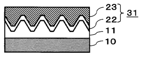
- Step (VI) is a step of forming a seed layer on the concavo-convex structure after the step (V) is applied, and step (VII) is a metal layer formed by electroforming (electroplating) on the seed layer.
- step (VIII) is a step of peeling the base material having the concavo-convex structure from the metal layer and the seed layer.
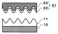
- FIG. 2 is a cross-sectional view schematically showing a transfer master 30 in which a layer 21 made of a first polymer segment having chevron-shaped irregularities is formed on a substrate 20, and FIG. FIG. 4 is a cross-sectional view schematically showing a state in which the seed layer 22 is formed on the surface irregularities of the layer 21 made of the first polymer segment in the master 30, and FIG. FIG. 5 is a cross-sectional view schematically showing a state in which the metal layer 23 and the seed layer 22 are peeled from the transfer master 30.
- the seed layer 22 is formed on the concavo-convex structure of the base material (transfer master 30) having the concavo-convex structure obtained after the step (V) (see FIGS. 2 and 3). ).
- the seed layer 22 is a layer that becomes a conductive layer for the subsequent electroforming process.
- the method for forming the seed layer 22 is not particularly limited, and a so-called conductive layer can be formed on the uneven layer 21 formed on the surface of the substrate 20 while maintaining the uneven shape. Possible known methods can be used as appropriate, and for example, they can be formed by methods such as electroless plating, sputtering or vapor deposition.
- the seed layer 22 has a thickness of 10 nm or more in order to make the current density uniform in the subsequent electroforming process and to keep the thickness of the metal layer deposited in the subsequent electroforming process constant. Is preferable, and it is more preferable that it is 100 nm or more.
- the seed layer material is not particularly limited. For example, nickel, copper, gold, silver, platinum, titanium, cobalt, tin, zinc, chromium, gold-cobalt alloy, gold-nickel alloy, boron- Nickel alloy, solder, copper / nickel / chromium alloy, tin / nickel alloy, nickel / palladium alloy, nickel / cobalt / phosphorus alloy, or alloys thereof can be used.
- the thickness of the metal layer 23 is not particularly limited.
- the thickness of the metal layer 23 including the thickness of the seed layer 22 may be 10 to 3000 ⁇ m as a whole.
- any of the above metal species that can be used as the seed layer 22 can be used.
- nickel is preferable from the viewpoint of wear resistance and releasability of the mold to be obtained. In this case, it is preferable to use nickel for the seed layer 22.
- the current density at the time of such electroforming is, for example, 0.03 to 10 A / cm 2 from the viewpoint of suppressing the bridge and forming a uniform metal layer and shortening the electroforming time. Good.
- the metal layer 23 performs processing such as pressing, peeling, and washing with respect to the resin layer when using the mold including the metal layer 23 and the seed layer 22, it is appropriate from the viewpoint of ease of the processing. It preferably has hardness and thickness. From such a viewpoint, for the purpose of improving the hardness of the metal layer 23 formed by electroforming, the surface of the metal mold may be subjected to diamond-like carbon (DLC) treatment or Cr plating treatment, or The metal layer 23 may be further heat treated to increase its surface hardness.
- DLC diamond-like carbon
- the metal part 31 composed of the metal layer 23 and the seed layer 22 is peeled from the base material (transfer master 30) having an uneven structure. (Step (VIII)).
- the master part (mold) for forming the diffraction grating can be obtained by peeling the metal part 31 composed of the seed layer 22 and the metal layer 23 thus obtained from the base material having the concavo-convex structure. In other words, in this way, a matrix 31 for forming a diffraction grating composed of the seed layer 22 and the metal layer 23 can be obtained.
- the method for peeling off such a diffraction grating forming matrix (mold) 31 is not particularly limited, and a known method can be used as appropriate, and a method of physically peeling off can be used.
- Method of peeling mold (metal part) 31 by dissolving and removing the homopolymer and the remaining block copolymer using an organic solvent that dissolves them, for example, toluene, tetrahydrofuran (THF), chloroform, etc. May be used.
- the mold 31 obtained in this way is obtained by transferring (reversing) the unevenness characteristics of the transfer master 30.
- the master 31 (mold) 31 for forming the diffraction grating is peeled from the master 30 for transfer (the substrate 10 on which the layer 21 having projections and depressions in the mountain structure is laminated), depending on the method of the peeling treatment, A part of the polymer such as the first polymer segment may remain attached to the surface of the mold. In such a case, it is preferable to remove the polymer adhered and remaining on the surface of the mold by washing.
- wet cleaning or dry cleaning can be used. Examples of the wet cleaning method include a method of removing by washing with an organic solvent such as toluene and tetrahydrofuran, a surfactant, and an alkaline solution.
- ultrasonic cleaning may be performed.
- the polymer remaining after adhering to the mold surface may be removed by electrolytic cleaning.
- the dry cleaning method include a method of removing by ashing using ultraviolet rays or plasma.
- the polymer remaining attached to the surface of the mold may be removed by washing using a combination of such wet washing and dry washing. Further, after such washing, rinsing with pure water or purified water may be performed, and ozone drying may be performed after drying.
- the method for manufacturing a matrix (mold) for forming a diffraction grating including the steps (I) to (VIII) has been described above. Manufacturing of a matrix (mold) for forming a diffraction grating having such irregularities is described.
- the method is not particularly limited, and a known method can be appropriately used.
- the block co-polymer obtained by carrying out steps (I) to (IV) (preferably also carrying out step (V)) is used.
- a resin layer having a concavo-convex structure derived from a combined microphase separation structure may be used as a mold as it is, or steps (I) to (IV) are carried out (preferably, step (V) is also carried out).
- a transfer material material other than the seed layer and the metal layer described above is formed on the surface of the concavo-convex structure of the resin layer. ) Is attached and cured, then removed Thus, an uneven transfer member having unevenness formed on the surface may be obtained and used as a mother mold (mold) for forming a diffraction grating.
- a transfer material is not particularly limited.
- silicone polymer silicone rubber
- urethane rubber norbornene resin
- polycarbonate polyethylene terephthalate
- polystyrene polymethyl methacrylate
- acrylic resin liquid crystal polymer
- epoxy resin epoxy resin
- the method for attaching such a transfer material is not particularly limited, and for example, vacuum deposition method; spin coating method, spray coating method, dip coating method, dropping method, gravure printing method, screen printing method, letterpress printing
- Various coating methods such as a method, a die coating method, a curtain coating method, an ink jet method, and a sputtering method can be employed.
- the conditions for curing the transfer material vary depending on the type of transfer material to be used.
- the curing temperature is in the range of room temperature to 250 ° C.
- the curing time is in the range of 0.5 minutes to 3 hours. Is preferred.
- a method of curing by irradiating energy rays such as ultraviolet rays or electron beams may be used.
- the irradiation amount is preferably in the range of 20 mJ / cm 2 to 10 J / cm 2 .
- a final mold may be manufactured by repeating the process of using the transfer material and repeating the inversion and transfer of the unevenness.
- the uneven shape of the final mold (mold) for forming the diffraction grating preferably has the same characteristics as the first unevenness described above.
- the shape of such irregularities can be easily adjusted by appropriately changing the type of polymer used, the heating conditions in the heating step, and the like.
- a diffraction grating forming material for example, a curable resin
- a transparent support substrate using the obtained diffraction grating forming matrix (mold) 31, and the diffraction grating is formed while pressing the matrix.
- the step of laminating the concavo-convex layer in which the concavo-convex is formed on the transparent support substrate by removing the matrix step of manufacturing a diffraction grating
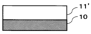
- FIG. 6 is a cross-sectional view schematically showing a state in which a diffraction grating forming material 11 ′ (for example, a resin material or a transparent inorganic layer forming material) is applied on the transparent support substrate 10
- FIG. 8 is a cross-sectional view schematically showing a state in which the diffraction grating forming material is cured while pressing the mold 31
- FIG. 8 is a schematic diagram in which irregularities are formed on the surface of the diffraction grating (first uneven layer) 11 by removing the mother mold 31.
- FIG. 11 ′ for example, a resin material or a transparent inorganic layer forming material
- a diffraction grating forming material 11 ′ for example, a curable resin
- the transparent support substrate 10 see FIG. 6
- the diffraction grating forming material is cured while pressing a diffraction grating forming mother mold (mold) 31 against the film of the diffraction grating forming material 11 ′ (see FIG. 7).
- Such a transparent support substrate 10 is the same as the transparent support substrate 10 described above. Moreover, as such a diffraction grating forming material 11 ′, the material (resin material or transparent inorganic layer forming material) described as a material for forming the first uneven layer (diffraction grating) 11 is used.
- a transparent inorganic layer forming material is used as such a diffraction grating forming material 11 ′ (when the concavo-convex layer is an inorganic layer)
- a sol solution containing a metal material it does not restrict
- the sol solution containing a silica precursor metal alkoxide
- Such silica precursors include tetramethoxysilane (TMOS), tetraethoxysilane (TEOS), tetra-i-propoxysilane, tetra-n-propoxysilane, tetra-i-butoxysilane, tetra-n- Tetraalkoxide monomers such as butoxysilane, tetra-sec-butoxysilane, tetra-t-butoxysilane, methyltrimethoxysilane, ethyltrimethoxysilane, propyltrimethoxysilane, isopropyltrimethoxysilane, phenyltrimethoxysilane, methyltrimethoxysilane Ethoxysilane, ethyltriethoxysilane, propyltriethoxysilane, isopropyltriethoxysilane, phenyltriethoxysilane, methyltripropoxysi
- the sol solution may be a sol solution capable of forming an inorganic layer by a sol-gel method
- the type of metal material is not particularly limited, and besides metal alkoxide, metal acetylacetonate, metal carboxylate , Oxychloride, chloride, and mixtures thereof.
- the metal species in such a metal material is not particularly limited, and any metal species other than silicon (Si) can be used to form an inorganic layer by a sol-gel method.
- Si silicon
- Ti, Sn, Al, Zn, Zr, In, or the like may be used as appropriate.
- 1 type may be used independently, or 2 or more types may be combined and utilized as a mixture.
- the precursor of the inorganic layer (The layer which consists of the said metal single-piece
- the mixture of TEOS and MTES for a sol solution those compounding ratios in particular are not restrict
- alcohols such as methanol, ethanol, isopropyl alcohol (IPA), butanol, aliphatic hydrocarbons such as hexane, heptane, octane, decane, cyclohexane, benzene, toluene, Aromatic hydrocarbons such as xylene and mesitylene, ethers such as diethyl ether, tetrahydrofuran and dioxane, ketones such as acetone, methyl ethyl ketone, isophorone and cyclohexanone, butoxyethyl ether, hexyloxyethyl alcohol, methoxy-2-propanol and benzyl Ether alcohols such as oxyethanol, glycols such as ethylene glycol and propylene glycol, ethylene glycol dimethyl ether, diethylene glycol dimethyl ether Ter, glycol ethers such as
- additives examples include polyethylene glycol, polyethylene oxide, hydroxypropyl cellulose, polyvinyl alcohol for viscosity adjustment, and alkanols such as triethanolamine, which is a solution stabilizer.
- alkanols such as triethanolamine, which is a solution stabilizer.
- alkanols such as triethanolamine, which is a solution stabilizer.
- examples include ⁇ -diketones such as amine and acetylacetone, ⁇ -ketoesters, formamide, dimethylformamide, and dioxane.
- the coating thickness of the diffraction grating forming material is preferably in the range where the thickness of the first uneven layer (diffraction grating) 11 is 0.01 to 500 ⁇ m (more preferably 0.5 to 500 ⁇ m). If the coating thickness of the diffraction grating forming material is less than the lower limit, the height of the unevenness formed on the surface of the first uneven layer tends to be insufficient. The influence of volume change that occurs during curing of (for example, resin) increases, and the uneven shape tends to be unable to be formed satisfactorily.
- Examples of the method for applying the diffraction grating forming material 11 ′ (including the sol solution) on the transparent support substrate 10 include spin coating, spray coating, dip coating, dropping, gravure printing, Various coating methods such as a screen printing method, a relief printing method, a die coating method, a curtain coating method, an ink jet method, and a sputtering method can be employed.
- the diffraction grating forming material is a resin material (for example, a curable resin)
- the conditions for curing the resin material vary depending on the type of resin used.
- the curing temperature is in the range of room temperature to 250 ° C.
- the curing time is preferably in the range of 0.5 minutes to 3 hours.
- the irradiation amount is preferably in the range of 20 mJ / cm 2 to 5 J / cm 2 .
- the diffraction grating forming material when cured using the sol solution (when an inorganic layer is formed), it can be used in a so-called sol-gel method depending on the metal species and the type of metal material to be used.
- the hardened layer (inorganic layer) may be formed from the sol solution by appropriately adopting known conditions. For example, when forming an inorganic layer (concave / convex layer) made of silica using a sol solution containing a silica precursor, the inorganic layer is formed by synthesizing amorphous silica by hydrolysis and polycondensation reactions. Can be formed.
- Such hydrolysis and polycondensation reaction is not particularly limited as long as it is a condition capable of synthesizing amorphous silica, but an acid such as hydrochloric acid or ammonia is used to adjust the pH of the sol solution. It is preferable to add an alkali such as, and more preferably, the pH is 4 or less or 10 or more.
- an alkali such as, and more preferably, the pH is 4 or less or 10 or more.
- water may be added separately.
- the addition amount of the water shall be 1.5 times or more by molar ratio with respect to metal alkoxide seed
- the diffraction grating forming matrix (mold) 31 is pressed against the coating film of the sol solution. Further, it is preferable to use a heated pressing roll. In this way, by pressing the mold while heating the coating film, the mold can be cured while being pressed, and the uneven layer tends to be formed more efficiently. In addition, after the transparent inorganic layer forming material is cured to form an inorganic layer in this way, it is further heated at a temperature of 200 to 1200 ° C. for 5 minutes to 6 hours from the viewpoint of increasing mechanical strength. It is preferable to do.
- the heat resistance of the diffraction grating 11 tends to be improved as compared with the case where a resin material is used. Therefore, when the diffraction grating 11 is formed of a transparent inorganic layer forming material, when it is used for manufacturing an organic EL element, a low-resistance transparent electrode (for example, ITO) is efficiently formed by so-called heat sputtering. In addition to obtaining a more power-efficient organic EL element, even when the organic EL element is used under high temperature conditions, the diffraction grating 11 is not discolored and the deterioration due to high temperature is more sufficiently suppressed. it can.
- the diffraction grating 11 is formed of a transparent inorganic layer forming material, it is possible to perform brush cleaning on the concavo-convex pattern surface of the diffraction grating 11 before elementization.
- the transparent inorganic layer forming material is used as a material for forming the uneven layer, the mechanical strength of the surface of the uneven layer is higher than when using a resin material, so brush cleaning Since it is possible to sufficiently suppress the generation of scratches on the surface of the layer by the process (because basically no scratches are generated), the surface of the concavo-convex layer can be efficiently cleaned, and foreign matters on the surface can be more efficiently removed.
- the occurrence of defects due to foreign matters on the surface can be sufficiently suppressed (the rate of occurrence of defects can be reduced). Furthermore, when the diffraction grating 11 is formed of a transparent inorganic layer forming material, it is possible to form a layer that is more excellent in chemical resistance than in the case of using a resin material, and the layer has a higher level of alkali resistance. It can also be improved. Therefore, various cleaning solvents can be used in the surface cleaning step. That is, it is possible to appropriately use an alkali or various organic solvents without selecting a cleaning liquid in the cleaning step before device fabrication.
- the diffraction grating 11 when the diffraction grating 11 is formed of a transparent inorganic layer forming material, a layer superior in chemical resistance can be formed as compared with the case of using a resin material. There is a tendency that damage caused by the resist and the developer can be further reduced.
- the UV resistance of the diffraction grating 11 when the diffraction grating 11 is formed of a transparent inorganic layer forming material, the UV resistance of the diffraction grating 11 can be made higher than that when a resin material is used. Therefore, when the diffraction grating 11 is formed of a transparent inorganic layer forming material, it is possible to efficiently clean and remove organic contaminants by UV ozone cleaning, and to reduce the defect rate derived from organic contaminants. In addition, it is possible to sufficiently suppress deterioration due to sunlight even when used outdoors, and to have a higher level of weather resistance.
- the mother die 31 is removed from the cured diffraction grating (first uneven layer) 11 (see FIG. 8).
- the method for removing the matrix 31 from the cured diffraction grating (first uneven layer) 11 is not particularly limited, and a known method can be appropriately employed.
- corrugation was formed on the transparent support substrate 10 can be laminated
- the mold when transferring the concavo-convex structure to a diffraction grating forming material (for example, a curable resin) using a mother mold (mold 31), the mold releasability from the diffraction grating forming material.
- the mold may be released.
- a mold release treatment a prescription for lowering the surface energy is common, and there is no particular limitation.
- a mold release agent such as a fluorine-based material or silicone resin is coated on the uneven surface of the mold 31 or fluorine.
- a method of treating with a silane coupling agent and a method of forming a diamond-like carbon film on the surface is provided.
- the transparent support substrate 10 including the diffraction grating 11 having a desired pattern can be obtained.
- the transparent support substrate 10 including the diffraction grating 11 thus obtained is used for forming the diffraction grating.
- the process of manufacturing the diffraction grating 11 may be performed again by using it as a mother mold. That is, an inverted pattern replica may be manufactured using the transparent support substrate 10 including the diffraction grating 11 as a matrix, and in this case, the replica may be used as the diffraction grating 11. Further, such inversion and transfer processes may be repeated. For example, the above replicating process may be repeated again using a replica of the inverted pattern as a matrix to form a child replica.
- the inversion and transfer of the unevenness may be repeated to finally form the diffraction grating 11 having the first unevenness.
- a film is deposited on the surface on which the concave / convex pattern of the diffraction grating (first concave / convex layer) used as a matrix is formed by a vapor phase method such as vapor deposition or sputtering. You may laminate.
- a resin for example, UV curable resin
- a deposited film examples include metals such as aluminum, gold, silver, platinum, and nickel, and metal oxides such as aluminum oxide.
- the thickness of such a film is preferably 5 to 500 nm. If the thickness is less than the lower limit, it is difficult to obtain a uniform film, and the effect of sufficiently reducing the adhesiveness is reduced. If the thickness exceeds the upper limit, the shape of the matrix tends to be distorted. When the uneven layer of the replica is made of a UV curable resin, post-cure may be appropriately performed by irradiating ultraviolet light again after the resin is cured.
- the microlens 12 is composed of a concavo-convex layer (second concavo-convex layer) having a second concavo-convex formed on the surface.
- a material (microlens forming material) for forming such a microlens (second concavo-convex layer) 12 the same material (for example, a curable resin as that used for manufacturing the diffraction grating 11 described above, Transparent inorganic layer forming material) can be used as appropriate.
- the microlens 12 (uneven layer) may be a cured resin layer obtained by curing the resin material or an inorganic layer formed using a transparent inorganic layer forming material.
- the thickness of the microlens (second uneven layer) 12 is preferably in the range of 1 to 500 ⁇ m.
- the thickness of the concavo-convex layer forming such a microlens 12 is less than the lower limit, the height of the concavo-convex formed on the surface of the concavo-convex layer tends to be insufficient, whereas when the thickness exceeds the upper limit, the microlens There is a tendency that the effect of volume change that occurs at the time of curing of the forming material (for example, resin) becomes large and the uneven shape cannot be formed satisfactorily.
- the concavo-convex analysis image obtained by analyzing the second concavo-convex shape formed on the surface using an atomic force microscope is subjected to a two-dimensional fast Fourier transform process.
- the Fourier transform image needs to show a circular or annular pattern substantially centered on the origin where the absolute value of the wave number is 0 ⁇ m ⁇ 1 .
- the concavo-convex shape is isotropic when viewed from all cross-sectional directions, When light is incident from the side of the surface (surface in contact with the substrate) and light is emitted from the surface on which the shape is formed, the angle dependency and chromaticity change of the emitted light are sufficiently reduced. It becomes possible.
- the circular or annular pattern of the Fourier transform image of the second concavo-convex shape exists in a region where the absolute value of the wave number is in the range of 1 ⁇ m ⁇ 1 or less.
- a Fourier transform image shows the above-mentioned conditions, by forming a concavo-convex shape on the surface of the concavo-convex layer, the angle dependency and chromaticity change of the emitted light are sufficiently reduced at a higher level. It becomes possible to do.
- the circular or annular pattern related to the second concavo-convex shape is such that the absolute value of the wave number is from the viewpoint of efficiently refracting or diffracting the emission spectrum in the visible region (380 nm to 780 nm). It is preferably present in a region in the range of 0.05 to 1 ⁇ m ⁇ 1 , and more preferably in a region in which the absolute value of the wave number is in the range of 0.1 to 0.5 ⁇ m ⁇ 1 .
- the circular or annular pattern does not exist in the region within the range of the absolute value of the wave number, that is, within the range among the bright spots of the Fourier transform image constituting the circular and annular pattern.
- the pattern of the Fourier transform image of the second unevenness is more preferably an annular shape from the viewpoint of obtaining a sufficient effect for light having a wavelength in the visible range (380 nm to 780 nm).
- a method for measuring the Fourier transform image a method similar to the method for measuring the Fourier transform image having the first uneven shape described above can be employed.
- the average pitch of the second irregularities formed on the surface of the microlens (second irregularity layer) 12 is preferably in the range of 2 to 10 ⁇ m, and preferably in the range of 2.5 to 5 ⁇ m. Is more preferable. If the average pitch of such irregularities is less than the lower limit, the diffraction effect as a diffraction grating is stronger than the refraction effect as a lens, and not only the light extraction effect is reduced, but also the angle dependency of the emitted light is high.
- the average pitch of such second irregularities is determined by measuring the pitch of the second irregularities on the surface of the second irregularity layer (the distance between adjacent convex parts or the distance between adjacent concave parts). It means the average value of pitch.
- the average value of the pitch of the second unevenness is determined by using a scanning probe microscope (for example, product name “E-sweep” manufactured by SII Nano Technology Co., Ltd.). After measuring the unevenness analysis image, the interval between any adjacent convex portions or adjacent concave portions in the unevenness analysis image is measured at 10 points or more, and a value calculated by calculating the average is adopted.
- the average height of the second irregularities formed on the surface of the microlens (second irregularity layer) 12 is preferably in the range of 400 to 1000 nm, more preferably in the range of 600 to 1000 nm. More preferably, it is in the range of 700 to 900 nm. If the average height (depth) of such irregularities is less than the lower limit, sufficient refraction or diffraction effects tend not to be obtained. On the other hand, when the upper limit is exceeded, the mechanical strength decreases, Cracks tend to occur during use.
- the average height of the unevenness means an average value of the height of the unevenness when the height of the unevenness on the surface of the uneven layer (the distance in the depth direction between the recessed portion and the protruding portion) is measured.
- the average height of such irregularities is obtained by analyzing the irregularities on the surface using a scanning probe microscope (for example, product name “E-sweep” manufactured by SII Nano Technology Co., Ltd.). After measuring the image, 10 or more distances in the depth direction with respect to arbitrary concave portions and convex portions in the unevenness analysis image are measured, and a value calculated by calculating the average is adopted.
- the uneven shape having such a height (depth) can be efficiently formed by using a method for manufacturing a microlens for an organic EL element of the present invention described later.
- y 0 ( ⁇ ) represents a theoretical value of an emission spectrum intensity at an angle ⁇ obtained from a radiation pattern based on Lambert's law at an angle of 0 ° obtained from the radiation pattern.
- the value normalized by the theoretical value of the emission spectrum intensity is shown.
- the second concavo-convex layer in which the sum of the squares of the difference between the normalized value of the measured value and the normalized value of the theoretical value is within the above range has a radiation pattern that approximates the radiation pattern according to the Lambert law. It is shown.
- the second uneven layer having such a total value within the above range can be used as the microlens 12 capable of sufficiently reducing the angle dependency of the emitted light.
- the sum of the squares of the difference between the normalized value of the measured value and the normalized value of the theoretical value ( ⁇ (y ( ⁇ ) ⁇ y 0 ( ⁇ )) 2 ) is a higher degree of the angle of the emitted light. Since it is possible to reduce dependency and change in chromaticity, it is more preferably 0.03 or less, and particularly preferably 0.01 or less.
- a method for obtaining a value (standardized value) obtained by standardizing the measured value of the emission spectrum intensity will be described.
- a known emission spectrum measuring apparatus for example, trade name “USB-2000” manufactured by Ocean Optics
- the light incident on the concavo-convex layer is obtained by laminating a light extraction transparent substrate for an organic EL element on the organic EL element, and using the organic layer of the organic EL element as a light source.
- a light source having a visible light emission spectrum such as a xenon lamp, a halogen lamp, a metal halide lamp, a sodium lamp, a mercury lamp, a fluorescent lamp, or an LED lamp may be used as a light source.
- the measurement angle when measuring from the direction perpendicular to the surface of the second uneven layer 12 is 0 °
- the measurement angles are ⁇ 80 °, ⁇ 75 °, ⁇ 10 °, ⁇ 5 °. , 0 °, 5 °, 10 °... 75 °, 80 °
- spectral data of light having a wavelength of 450 to 700 nm are respectively measured at 33 measurement positions, and from the integrated area of the spectral data at each angle.
- the central portion of the light receiving surface that receives the emission spectrum of the emission spectrum measuring apparatus is defined as the light receiving unit O, and the second unevenness.
- a direction that passes through the measurement point P and is perpendicular to the surface S of the second concavo-convex layer (indicated by a dotted arrow A in FIG. 2).
- the angle formed by the line segment PO (line L1) connecting the light receiving unit O and the measurement point P with respect to the “dotted line A” in some cases is referred to as a measurement angle ⁇ .
- the spectrum is measured such that the distance between the measurement point P and the light receiving unit O is 10 cm.
- the value (y (0)) obtained by standardizing the measured value of the emission spectrum intensity at the measurement angle of 0 ° is 1.0.
- the radiation pattern based on the Lambert law is a pattern of angular distribution (so-called Lambert distribution) of emission spectrum intensity (integrated area value of a spectrum of light having a wavelength of 450 to 700 nm) theoretically obtained by the Lambert law. .
- the theoretical value of the emission spectrum intensity at the measurement angle of 33 points is calculated as the theoretical value of the emission spectrum intensity at the angle of 0 °.
- the normalized value (y 0 ( ⁇ )) obtained by normalizing the theoretical value of the emission spectrum intensity at each angle ⁇ is 1.0.
- the microlens (second uneven layer) 12 employs a method similar to the method for measuring the emission spectrum intensity, etc., and measures the emission spectrum intensity of light having a wavelength of 380 to 780 nm.
- the maximum value of the distance ( ⁇ c) between the color coordinate at the measurement angle of 0 ° and the color coordinate at each measurement angle is 0.015 or less, preferably Is preferably 0.01 or less, more preferably 0.006 or less.
- the maximum value of the color coordinate distance exceeds the upper limit, the viewing angle dependency of the emission color increases, and when the angle is changed, the color change tends to be perceivable by humans.
- the microlens (second uneven layer) 12 may be laminated on the transparent support substrate 10 via an adhesive layer and / or an adhesive layer.
- the pressure-sensitive adhesive layer and / or the adhesive layer are thus included, for example, a method of laminating the microlens 12 using an adhesive on a transparent support substrate, or a micro-layer using a pressure-sensitive adhesive on the transparent support substrate 10
- the microlens (second concavo-convex layer) 12 may be laminated on the transparent resin substrate 10 using a method of laminating the lenses 12 or the like. In this case, it is also possible to separately manufacture the microlens (second uneven layer) 12 in the form of a film and paste it on the surface of the transparent resin substrate 10 in that form.
- a known material capable of bonding the microlens (second uneven layer) 12 on the transparent support substrate 10 is used.
- a known material pressure-sensitive adhesive and adhesive capable of bonding the microlens (second uneven layer) 12 on the transparent support substrate 10 is used.
- Synthetic rubber-based adhesives such as coalescence, polyurethane-based adhesives, and polyester-based adhesives may be used as appropriate, and commercially available products (Noland UV-curable optical adhesives NOA60, NOA61, NOA71, NOA72, NOA81, Toa Synthetic UV-3400) may be used.
- the method for applying such a pressure-sensitive adhesive and adhesive is not particularly limited, and a known
- the microlens (second concavo-convex layer) 12 has a protective layer laminated on the surface on which the concavo-convex shape is formed from the viewpoint of improving the friction resistance and scratch resistance of the second concavo-convex on the surface. It is preferable.
- a protective layer a transparent film or a transparent inorganic vapor deposition layer can be used as appropriate. Such a transparent film is not particularly limited, and a known transparent film can be appropriately used.
- polyester resins such as polyethylene terephthalate, cellulose resins, acetate resins, polyethersulfone resins, polycarbonates
- a film made of a transparent polymer such as a resin, a polyamide resin, a polyimide resin, a polyolefin resin, and an acrylic resin.
- a transparent film forms a pressure-sensitive adhesive layer or an adhesive layer on one surface, and a space is formed between the convex portions on the surface of the second concave-convex layer on which the second concave-convex portions are formed. In this way, a transparent film may be bonded and used.
- pressure-sensitive adhesives or adhesives examples include acrylic pressure-sensitive adhesives, ethylene-vinyl acetate copolymers, natural rubber pressure-sensitive adhesives, polyisobutylene, butyl rubber, styrene-butylene-styrene copolymers, and styrene-imprene- Synthetic rubber adhesives such as styrene block copolymers, polyurethane adhesives, and polyester adhesives may be used as appropriate.
- a known metal material capable of forming a transparent inorganic layer by vapor deposition can be used as appropriate, for example, Sn, In, Te, Examples thereof include oxides, nitrides, and sulfides of metals such as Ti, Fe, Co, Zn, Ge, Pb, Cd, Bi, Se, Ga, and Rb.
- a metal material TiO 2 can be preferably used from the viewpoint that deterioration due to oxidation can be sufficiently prevented, and ZnS is preferably used from the viewpoint that low luminance and high luminance can be obtained. Can be used.
- limit especially as a method of forming such an inorganic vapor deposition layer What is necessary is just to manufacture suitably using a well-known physical vapor deposition apparatus.
- a method for manufacturing such a microlens 12 will be described.
- the following method (B) for producing a microlens can be suitably employed.
- a microlens forming material for example, a resin material (such as a curable resin) or a transparent inorganic layer forming material
- Such a method (B) is a method using a mother mold (mold) for forming a microlens. As such a mold, it is cured while being pressed against a layer made of an uncured microlens forming material, whereby the shape of the unevenness formed on the mold is transferred (reversed) and explained in the microlens 12. What is necessary is just to be able to form the second uneven layer on which the second unevenness is formed. Therefore, such a mold having a concavo-convex shape on its surface is used, and the concavo-convex shape characteristics (average height, average pitch, etc.) are formed on the surface of the second concavo-convex layer forming the microlens 12 described above. It is preferable that it has the same characteristic as the unevenness
- the method for producing such a mold (mold) for forming a microlens is not particularly limited, but in particular, on the surface of a polymer film made of a polymer whose volume changes by heat under a temperature condition of 70 ° C. or higher.
- FIG. 10 is a cross-sectional view schematically showing a state in which the polymer film 41 before the vapor deposition film is formed is laminated on the polymer film forming substrate 40, and FIG.
- FIG. 11 is a diagram showing vapor deposition on the polymer film 41.
- FIG. 12 is a cross-sectional view schematically showing a state in which the film 42 is formed and the polymer film 41 and the vapor deposition film 42 are cooled to form irregularities due to wrinkles on the surface of the vapor deposition film 42.
- FIG. 13 is a cross-sectional view schematically showing a state in which the matrix material 43 ′ is attached on the vapor deposition film 42.
- FIG. 13 shows the matrix 43 obtained by curing the matrix material 43 ′ removed from the vapor deposition film 42. It is sectional drawing which shows a state typically.
- a polymer film 41 made of a polymer whose volume is changed by heat is prepared on the polymer film forming substrate 40.
- a polymer whose volume is changed by heat a polymer whose volume is changed by heating or cooling (for example, a coefficient of thermal expansion of 50 ppm / K or more) can be appropriately used.
- a silicone polymer is more preferable. Particularly preferred is a silicone-based polymer containing.
- the method for forming such a polymer film 41 is not particularly limited.
- spin coating, dip coating, dropping, gravure printing, screen printing, letterpress printing, die coating, curtain coating A method of applying the polymer on the polymer film forming substrate 40 that can support the polymer film by employing a method, an ink jet method, a spray coating method, a sputtering method, a vacuum deposition method, or the like can be employed. .
- the polymer film forming substrate 40 is not particularly limited, and a known substrate (glass substrate or the like) that can be used when forming a polymer film can be used as appropriate.
- the thickness of the polymer film 41 thus formed is preferably in the range of 10 to 5000 ⁇ m, and more preferably in the range of 10 to 2000 ⁇ m.
- the polymer film 41 is used while being laminated on the substrate 40, but the polymer film 41 may be used by being detached from the substrate 40.
- step (i) after preparing the polymer film 41 as described above, the vapor deposition film 42 is formed on the surface of the polymer film 41 under a temperature condition of 70 ° C. or higher.
- the temperature at which the vapor deposition film 42 is formed needs to be 70 ° C. or higher, and more preferably 90 ° C. or higher. If the said temperature is less than 70 degreeC, the unevenness
- a known method such as a vapor deposition method or a sputtering method can be appropriately employed.
- the material of the vapor deposition film 42 is not particularly limited, and examples thereof include metals such as aluminum, gold, silver, platinum, and nickel, and metal oxides such as aluminum oxide.
- the step (i) after forming the vapor deposition film 42 on the surface of the polymer film 41 as described above, the polymer film 41 and the vapor deposition film 42 are cooled, so that the surface of the vapor deposition film 42 is uneven by wrinkles. (See FIG. 11).
- the vapor deposition film 42 is formed on the polymer film 41 and then cooled, the volumes of the polymer film 41 and the vapor deposition film 42 change, but the thermal expansion coefficient of the material forming the polymer film 41 and the vapor deposition film 42 are reduced. Since there is a difference between the coefficient of thermal expansion of the material to be formed, the rate of change in volume of each layer is different, and as shown in FIG.
- the surface of the vapor deposition film 42 has irregularities (so-called buckling pattern, Alternatively, a so-called Turing pattern) is formed.
- the temperature of the polymer film 41 after cooling and the vapor deposition film 42 is 40 degrees C or less.
- the cooling rate when cooling the polymer film 41 and the deposited film 42 is preferably in the range of 1 to 80 ° C./min.
- the temperature lowering rate is less than the lower limit, the unevenness tends to be relaxed, and when it exceeds the upper limit, scratches such as cracks tend to occur on the surface of the polymer film or the deposited film.
- Step (ii) is a step of obtaining a matrix for forming a microlens by removing the cured matrix material from the deposited film after depositing and curing the matrix material on the deposited film.
- a matrix material 43 ′ is adhered on the surface of the vapor deposition film 42 (a surface having an uneven shape) (see FIG. 8).
- the matrix material 43 ′ is not particularly limited as long as the obtained matrix can maintain strength, hardness, and the like for use as an uneven mold.
- nickel Silicon, silicon carbide, tantalum, glassy carbon, quartz, silica, etc .
- silicone polymers silicone rubber), urethane rubber, norbornene resin, polycarbonate, polyethylene terephthalate, polystyrene, polymethyl methacrylate, acrylic, liquid crystal polymer, etc.
- a resin composition is mentioned.
- silicone-based polymers, nickel, silicon, silicon carbide, tantalum, glassy carbon, quartz, and silica are more preferable from the viewpoint of moldability, followability of fine shapes, and mold release, and silicone-based materials are preferable.
- the polymer is even more preferable, and a silicone-based polymer containing polydimethylsiloxane is particularly preferable.
- the method of attaching the matrix material 43 ′ to the surface of the deposited film 42 on which the uneven shape is formed is not particularly limited.
- electroplating vacuum deposition method; spin coating method, spraying
- Various coating methods such as a coating method, a dip coating method, a dropping method, a gravure printing method, a screen printing method, a relief printing method, a die coating method, a curtain coating method, an ink jet method, and a sputtering method can be employed.
- step (ii) the matrix material 43 ′ is adhered on the surface of the vapor deposition film 42 as described above, and then the matrix material 43 ′ is cured.
- the conditions for curing the matrix material 43 ′ vary depending on the type of the matrix material to be used, and cannot be generally stated. For example, when a resin material is used, depending on the type of the material
- the curing temperature is preferably in the range of room temperature to 250 ° C.
- the curing time is preferably in the range of 0.5 minutes to 3 hours.
- a method of curing the matrix material 43 ′ by irradiating energy rays such as ultraviolet rays or electron beams may be employed. Is preferably in the range of 20 mJ / cm 2 to 10 J / cm 2 .
- the matrix material 43 ′ is cured on the surface of the vapor deposition film 42 as described above, and then the matrix material 43 ′ is cured as shown in FIG.
- a mother lens 43 for forming a microlens is obtained.
- the method for removing the mother die 43 from the vapor deposition film 42 is not particularly limited, and a known method can be adopted as appropriate.
- a curable resin is applied on one surface of the support material, the curable resin is cured while pressing the mother die 43, and the mother die 43 is removed, whereby a first unevenness is formed on the support material.
- the polymer film and the vapor deposition film are cooled to form irregularities due to wrinkles on the surface of the vapor deposition film.
- the 3rd process of obtaining a layered product After a curable resin is applied on one surface of another support material to obtain a coating film, the curable resin is cured while pressing the uneven surface of the laminate against the coating film, and the laminate is removed.
- a fourth step of obtaining a second concavo-convex resin film having irregularities formed on the support material A fifth step of obtaining a matrix by removing the matrix material after curing from the deposited film after the matrix material is attached and cured on the second uneven resin film; May be further implemented.
- first to fifth steps may be repeatedly performed using the matrix obtained by the fifth step, or after the first to fifth steps are performed, the fifth step can be used. Only the third to fifth steps may be repeated using the uneven surface of the mother die as the surface having the unevenness described in the third step. Moreover, you may utilize the uneven
- the average height of the unevenness formed on the surface of the mother die can be increased. In this way, it is possible to form a microlens with higher performance by using the mother die with the average height of the unevenness as the mother die for forming the microlens.
- a process for replicating the concavo-convex shape formed on the first matrix for example, , The number of repetitions of the first to fifth steps), the type of the repeated steps, and the like can be changed as appropriate, whereby the characteristics of the unevenness can be easily adjusted. It can have similar characteristics.
- the same polymer as described in the step (i) can be used.
- the same resin material (curable resin) used when forming the first uneven layer can be used as appropriate.
- the supporting material is not particularly limited as long as it can apply and support a curable resin, and a known base material can be used as appropriate.
- the base material which becomes is mentioned.
- the coating method and curing method of the curable resin are not particularly limited, and the above-described resin material (curable resin) coating method and curing method may be appropriately employed.
- the third step is the same as the step described in the above-described uneven shape forming step, except that the polymer film obtained in the second step is used.
- the same resin material (curable resin) used for forming the first uneven layer can be used as appropriate.
- the matrix material used in the fourth step and the fifth step can be the same as described in the above step (ii), and the coating method thereof has also been described in the above step (ii). A method similar to the method may be used.
- the obtained matrix is used as a polymer film, and each step ( i) to (ii) may be repeated. Also by such a method, the wrinkles formed on the surface of the mother die can be deepened, and the average height of the irregularities formed on the surface of the mother die can be increased.
- a desired concavo-convex shape can be obtained by appropriately changing the design of the concavo-convex structure for the purpose of the type of resin to be used and repeated steps. Can be easily formed.
- the method for manufacturing the microlens forming mold (mold) including the steps (i) to (ii) has been described above, but the method for manufacturing the microlens forming mold (mold) is not particularly limited and is publicly known. Can be used as appropriate.
- a microlens-forming matrix in which a desired unevenness is formed by adopting a method similar to the above-described method of manufacturing a diffraction grating-forming matrix (mold)
- Mold may be manufactured.
- a method of performing steps (i) to (ii) may be used as a method of manufacturing a master (mold) for forming a diffraction grating.
- a microlens forming material for example, a resin material (curable resin) or a transparent inorganic layer is formed on one surface of a planar support material.
- the material is applied, and the microlens forming material is cured while pressing the matrix for forming the microlens, and then the mother mold is removed to form a second concavo-convex layer having irregularities formed on the surface ( The microlens forming step will be described.
- a microlens forming material for example, a curable resin
- a microlens forming material for example, a curable resin
- the microlens is pressed while pressing a matrix for forming the microlens.
- the forming material is cured.
- a material similar to the material for forming the first uneven layer (diffraction grating forming material) described above can be appropriately used.
- the planar support material is not particularly limited as long as it can apply and support the microlens forming material, and is not particularly limited, and may be a known substrate (for example, a glass substrate or a resin film ( TAC, PET, COP, PC, etc.), etc.) can be used as appropriate.
- the transparent support substrate 10 for organic EL elements can also be used suitably.
- the microlens (second concavo-convex layer) is not peeled off from the support material, and is used as it is for the production of a light extraction transparent substrate for an organic EL element. It is also possible to simplify the manufacturing process of the organic EL element. In particular, when a substrate in which the diffraction grating 11 is formed on the transparent support substrate 10 is used as the support material, the light extraction transparent substrate for an organic EL element can be used as it is. Moreover, using the resin film (TAC, PET, COP, PC, etc.) as the support material, a microlens is obtained in a state of being laminated on the film, and the film is laminated on the transparent support substrate 10. You may laminate.
- the thickness of such a support material is not particularly limited, but is preferably in the range of 1 to 500 ⁇ m.
- the microlens forming matrix is removed from the cured layer to obtain a microlens composed of the second uneven layer.
- the method for removing the matrix from the concavo-convex layer after curing is not particularly limited, and a known method can be adopted as appropriate. In this manner, a microlens composed of the second uneven layer in which the second unevenness is formed on the support material can be obtained.
- the microlens is peeled from the support material, and this is laminated on the transparent support substrate 10 via the pressure-sensitive adhesive layer and / or the adhesive layer, and the organic EL.
- a light extraction transparent substrate for the element may be manufactured, and when the transparent support substrate 10 is used as a support material, the light extraction transparent substrate may be used as it is without peeling the microlens.
- a transparent resin film or the like is used as the support material, a film in which microlenses are laminated may be laminated on the transparent support substrate 10 as it is.
- the method of manufacturing the light extraction transparent substrate including the transparent support substrate 10, the diffraction grating 11, and the microlens 12 is not particularly limited.
- the transparent support substrate 10 on which the diffraction grating 11 is previously laminated is separately provided.
- a method of stacking the manufactured microlenses 12 may be used, or a method of directly manufacturing the microlenses 12 on the other surface of the transparent support substrate 10 on which the diffraction grating 11 is previously stacked may be used.
- a method of directly manufacturing the diffraction grating 11 on the other surface of the transparent support substrate 10 on which the microlenses 12 are previously laminated may be used.
- the surface 10A on the side where the diffraction grating 11 of the transparent support substrate 10 is formed is used as the light L from the organic EL element.
- the surface 10B on which the microlens 12 of the transparent support substrate 10 is formed is disposed on the surface (exiting surface) side from which the light L from the organic EL element is emitted. To do. By utilizing in this way, it becomes possible to extract light from the organic EL more efficiently.
- the light extraction transparent substrate 1 uses the diffraction grating 11 and the microlens 12 in combination, the light emission efficiency can be sufficiently improved without increasing the average height of the irregularities of the diffraction grating. Therefore, it is possible to sufficiently suppress a decrease in the lifetime of the organic EL element and to sufficiently extract guided light. Further, in such a light extraction transparent substrate 1, the luminous efficiency can be sufficiently improved while sufficiently reducing the angle dependency of luminance and chromaticity.
- the light extraction transparent substrate for the organic EL element of the present invention is not limited to the above embodiment.
- the transparent support substrate 10, the diffraction grating 11, and the microlens 12 are included.
- an adhesive layer, a pressure-sensitive adhesive layer, a transparent resin layer for example, a resin film (TAC, PET, COP, PC, etc. that can be used for an organic EL element) between the transparent support substrate 10 and the microlens 12. Film etc.
- the resin film used as a support material at the time of manufacture of a microlens may be used as it is as a transparent resin layer.
- Etc. may be appropriately arranged, for example, in the organic EL element shown in FIG. It is good also as a structure of a laminated body like the light extraction transparent substrate 1.
- the organic EL element of the present invention includes a transparent support substrate, A diffraction grating comprising a first concavo-convex layer disposed on one surface side of the transparent support substrate and having a first concavo-convex formed on the surface; A microlens composed of a second concavo-convex layer disposed on the other surface side of the transparent support substrate and having a second concavo-convex formed on the surface; and A transparent electrode, an organic layer, and a metal electrode are sequentially stacked on the first uneven layer so that the shape of the first unevenness formed on the surface of the first uneven layer is maintained. And A component formed by the transparent support substrate, the diffraction grating, and the microlens is composed of the light extraction transparent substrate for the organic EL element of the present invention.
- FIG. 14 is a cross-sectional view schematically showing a preferred embodiment of the organic EL element of the present invention.
- the organic EL element shown in FIG. 14 basically includes a light extraction transparent substrate 1, a transparent electrode 51, an organic layer 52, a cathode buffer layer 53, and a metal electrode 54.
- the light extraction transparent substrate of the present invention is used.
- the microlens 12 is laminated as the light extraction transparent substrate 1 on the surface of the transparent support substrate 10 on the emission surface side of the organic EL element via the adhesive layer 13 and the transparent resin layer 14.
- a diffraction grating 11 is laminated on the other surface.
- Such a laminated structure between the microlens 12 and the transparent support substrate 10 uses a transparent resin film as a planar support substrate when the microlens 12 is manufactured, and is provided on the other surface of the transparent resin film. This can be easily achieved by forming an adhesive layer and pasting it on the transparent support substrate 10.
- the average height of the irregularities formed on the diffraction grating in the light extraction transparent substrate 1 is preferably 20% to 80% of the total thickness of the organic layer 52 of the organic EL element.
- the average height of such irregularities is less than the above lower limit (when it is less than 20%), the average height of the irregularities is insufficient, so that a sufficient diffraction effect tends not to be obtained.
- defects such as short circuit between the anode and the cathode, dielectric breakdown of the light emitting layer, defective light emission, reduced life, etc. tend to increase. It is in.
- the shape of the first unevenness is maintained on the surface of the diffraction grating (first uneven layer) 11 of the light extraction transparent substrate 1 on which the first unevenness is formed.
- the transparent electrode 51, the organic layer 52 (hole transport layer 101 / light emitting layer 102 / hole blocking layer 103 / electron transport layer 104), the cathode buffer layer 53, and the metal electrode 54 are sequentially laminated.
- the material of the transparent electrode 51 for example, indium oxide, zinc oxide, tin oxide, and indium tin oxide (ITO) which is a composite thereof, gold, platinum, silver, and copper are used. Among these, ITO is preferable from the viewpoint of balance between transparency and conductivity.
- the thickness of the transparent electrode 51 is preferably in the range of 20 to 500 nm. If the thickness is less than the lower limit, the conductivity tends to be insufficient. On the other hand, if the thickness exceeds the upper limit, the transparency is insufficient and the emitted EL light tends not to be taken out sufficiently.
- the organic layer 52 is a stacked body including a hole transport layer 101, a light emitting layer 102, a hole blocking layer 103, and an electron transport layer 104.
- the materials for the hole transport layer 101, the light emitting layer 102, the hole blocking layer 103, and the electron transport layer 104 are not particularly limited, and known materials can be appropriately used.
- the material of the hole transport layer 101 includes naphthyldiamine ( ⁇ -NPD), triphenylamine, triphenyldiamine derivative (TPD), derivatives such as benzidine, pyrazoline, styrylamine, hydrazone, triphenylmethane, carbazole, etc. Can be used.
- a material of the light emitting layer 102 for example, a material obtained by doping 4,4′-N, N′-dicarbazole-biphenyl (CBP) with trisphenylpyridinatoiridium (III) complex (Ir (ppy) 3 ), 8-hydroxyquinoline aluminum (Alq 3 , green, small molecule), bis- (8-hydroxy) quinaldine aluminum phenoxide (Alq ' 2 OPh, blue, small molecule), 5,10,15,20-tetraphenyl-21H, 23H -porphine (TPP, red, small molecule), poly (9,9-dioctylfluorene-2,7-diyl) (PFO, blue, polymer), poly [2-methoxy-5- (2'-ethylhexyloxy) -1 , 4- (1-cyanovinylene) phenylene] (MEH-CN-PPV, red, polymer), a material made of a fluorescent organic solid such
- hole blocking layer 103 a material known as a so-called hole blocking material (for example, 9-dimethyl-4,7-diphenyl-1,10-phenanthroline (BCP) or the like) can be used as appropriate.
- a material for the electron transport layer 104 an aluminum quinolinol complex, a phenanthroline derivative, an oxadiazole derivative, a triazole derivative, a phenylquinoxaline derivative, a silole derivative, or the like can be used.
- the positive hole transport layer 101, the light emitting layer 102, the positive hole blocking layer 103, and the electron transport layer 104 are maintained from the viewpoint of maintaining the uneven shape formed on the surface of the uneven layer.
- a transport layer 104) is preferred.
- the total thickness of the organic layer 52 is preferably in the range of 20 to 600 nm.
- the material of the cathode buffer layer 53 metal fluorides such as lithium fluoride (LiF) and Li 2 O 3 , highly active alkaline earth metals such as Ca, Ba, and Cs can be used.
- the thickness of the cathode buffer layer 53 is preferably in the range of 0.5 to 10 nm.
- the metal electrode 54 is an electrode made of metal.
- a substance having a small work function can be appropriately used, and is not particularly limited, and examples thereof include aluminum, MgAg, MgIn, and AlLi.
- the thickness of the metal electrode 54 is preferably in the range of 50 to 500 nm. When the thickness is less than the lower limit, the conductivity tends to decrease, and when the thickness exceeds the upper limit, the uneven shape tends to be difficult to maintain.
- the transparent electrode 51, the organic layer 52, the cathode buffer layer 53, and the metal electrode 54 are formed on the surface of the first concavo-convex layer of the diffraction grating, respectively. Is maintained on the surface of the first concavo-convex layer of the diffraction grating, so that the stress generated when the organic EL element is bent can be relaxed by the concavo-convex shape. Therefore, the organic EL element of the present invention can be suitably used as an organic EL element that requires flexibility such as a flexible display and flexible illumination.
- the diffraction grating 11 in the light extraction transparent substrate 1 has the condition indicated by the inequality (1) and / or the peak from the viewpoint of sufficiently suppressing the generation of leakage current. More preferably, the degree (k) satisfies the condition of -1.2 or more (more preferably -1.2 to 1.2).
- the light extraction transparent substrate 1 including the diffraction grating (first uneven layer) 11 satisfying such a condition is used, as shown in FIG. 15, the transparent electrode 51, the organic layer 52, and the metal electrode 54 (see FIG.
- the description of the cathode buffer layer 53 is omitted.
- each layer is a layer having a uniform thickness in a direction perpendicular to the surface of the transparent electrode substrate
- the surface of the transparent electrode substrate obtained on the basis of the unevenness analysis image of the first uneven layer 11
- the inter-electrode distance between the transparent electrode 51 and the metal electrode 54 in the vertical direction standard distance: the distance represented by X in FIG. 15
- the inter-electrode distance between the transparent electrode 51 and the metal electrode 54 are Shortest distance With respect to (shortest distance: distance represented by Y in FIG.
- the ratio of the measurement points at which the magnitude of the shortest distance Y is less than half of the standard distance X among all measurement points in the unevenness analysis is 0-2. %.
- the present inventors have found that a leak current tends to occur in a region where the size of the shortest distance Y is not more than half of the standard distance X, and based on such knowledge By making the ratio of the region in which the size of the shortest distance Y is half or less of the standard distance X be 0 to 2%, it is possible to sufficiently suppress the occurrence of leakage current. To find out.
- the ratio of the region (measurement point) in which the magnitude of the shortest distance Y is less than or equal to half of the standard distance X out of all the regions (all measurement points) is referred to as “leakage current”. It is called “the ratio of concern areas”
- the same method as the measuring method of the median value (M) and average value (m) of the depth distribution is adopted.
- the unevenness analysis image of the first uneven layer 11 is measured, and it is assumed that the transparent electrode 51, the organic layer 52, and the metal electrode 54 maintain the uneven shape formed on the surface of the first uneven layer 11 as it is.
- the size of the shortest distance Y among all the measurement points of the unevenness analysis image obtained from the distribution of the interelectrode distance is half of the standard distance X.
- the ratio of the measurement points (existence ratio of the leakage current concern region) to be 0 to 2% is as follows. That is, in the organic EL element of the present invention, it is preferable that the existence ratio of the leakage current concern region obtained from the distribution of the interelectrode distance between the transparent electrode 51 and the metal electrode 54 is 0 to 2%.
- the standard distance X is preferably set (assumed) in the range of 30 to 500 nm according to the actual design. For example, the standard distance X is perpendicular to the transparent support substrate of the organic layer.
- the standard distance X is assumed to be 70 nm. Then, the distribution of the shortest distance is calculated based on the unevenness analysis image (SPM image), and the region where the shortest distance Y between the electrodes is less than half of the standard distance X (leakage current concern region) is the unevenness analysis image. (SPM image)
- the ratio of the leakage current concern region can be determined by calculating the proportion of all the measurement points in the measurement. Note that the calculation of the shortest distance and the existence ratio of the leakage current concern region can be calculated by a computer based on the analysis result of the unevenness analysis image of the diffraction grating (first uneven layer) 11.
- the transparent electrode 51, the organic layer 52, the cathode buffer layer 53, and the metal electrode 54 are formed on the surface of the diffraction grating (first uneven layer) 11. Since the layers are stacked so as to maintain the shape, it is possible to prevent light generated in the organic layer from being totally reflected at each interface and repeating multiple reflections inside the element. Further, the light reflected at the interface between the transparent support substrate and the microlens 12 can be re-emitted by the diffraction effect. Furthermore, the transparent electrode 51, the organic layer 52, and the metal electrode 54 are laminated so that the shape of the first unevenness formed on the surface of the diffraction grating (first uneven layer) 11 is maintained, respectively.
- the distance between the transparent electrode 51 and the metal electrode 54 is partially shortened. Therefore, as compared with a case where the distance between the transparent electrode 51 and the metal electrode 54 is uniform, an increase in electric field strength can be expected when a voltage is applied, and the light emission efficiency of the organic EL element can also be improved. Further, when the leakage current concern region is controlled to be 0 to 2%, the leakage current can be sufficiently prevented, and the light emission efficiency of the organic EL element can be further improved. Thus, according to the organic EL element of the present invention, it is possible to achieve sufficient external extraction efficiency.
- the microlens 12 is disposed on one surface of the transparent support substrate 10.
- a microlens 12 in the case of obtaining a Fourier transform image by applying a two-dimensional fast Fourier transform process to a second uneven shape (the unevenness analysis image obtained by analyzing the shape with an atomic force microscope).
- the Fourier transform image is formed in a shape showing a circular or annular pattern whose center is the origin whose wave number has an absolute value of 0 ⁇ m ⁇ 1 , and such irregularities are viewed from all cross-sectional directions.
- This is an isotropic uneven shape so that not only the light extraction efficiency is sufficiently high, but also light can be emitted sufficiently stably at all angles, and the angle dependence and color of the emitted light The change in the degree can be sufficiently reduced.
- the method for manufacturing such an organic EL element of the present invention is not particularly limited, and for example, a method for manufacturing an organic EL element as described below may be adopted. That is, as a method for producing such an organic EL element, a step of preparing a light extraction transparent substrate for the organic EL element of the present invention, and a first unevenness of the light extraction transparent substrate for the organic EL element are provided. On the surface of the layer (diffraction grating), the transparent electrode, the organic layer, and the metal electrode are respectively maintained such that the shape of the first unevenness formed on the surface of the first uneven layer is maintained. You may employ
- each process will be described with reference to an example in which the organic EL element of the embodiment shown in FIG. 14 is manufactured.
- the method for producing the light extraction transparent substrate described in the above-mentioned light extraction transparent substrate for the organic EL element of the present invention can be appropriately employed. .
- the transparent electrode 51 is formed on the surface of the first uneven layer 11 on the diffraction grating (first uneven layer) 11. Lamination is performed so that the uneven shape is maintained.
- the material of the transparent electrode 51 the same materials as those described as the material of the transparent electrode 3 in the organic EL element of the present invention can be used.
- a known method such as a vapor deposition method or a sputtering method can be appropriately employed. Among these methods, it is preferable to employ a vapor deposition method from the viewpoint of maintaining the shape of the first unevenness formed on the surface of the first uneven layer.
- the organic layer 52 is maintained on the transparent electrode 51 and the shape of the first unevenness formed on the surface of the first uneven layer 11 is maintained. Laminate as described. As a kind and material of such an organic layer 52, the thing similar to what was demonstrated regarding the organic layer in the organic EL element of the said this invention can be used.
- the organic layer 52 is, for example, a stacked body composed of a hole transport layer 101 / a light emitting layer 102 / a hole blocking layer 103 / an electron transport layer 104 as shown in FIG. 14 (the symbol “/” is stacked). May be configured.
- a known method such as a vapor deposition method or a sputtering method can be appropriately employed.
- a vapor deposition method from the viewpoint of maintaining the shape of the first unevenness formed on the surface of the first uneven layer 11.
- the cathode buffer layer 53 and the metal electrode 54 are formed on the surface of the first uneven layer 11 on the organic layer 52.
- the first irregularities are laminated so that the shape of the first irregularities is maintained.
- materials for the cathode buffer layer 53 and the metal electrode 54 the same materials as those described in the organic EL device of the present invention can be used.
- a method for laminating the cathode buffer layer 53 and the metal electrode 54 a known method such as a vapor deposition method or a sputtering method can be appropriately employed. Among these methods, it is preferable to employ a vapor deposition method from the viewpoint of maintaining the shape of the first unevenness formed on the surface of the first uneven layer 11.
- the method for producing the organic EL element is not limited to the above method, and a diffraction grating is formed on the transparent support substrate, and the organic EL element forming step is performed on the diffraction grating. Then, after obtaining a laminate of the transparent support substrate 10, the diffraction grating 11, the transparent electrode 51, the organic layer 52, the cathode buffer layer 53, and the metal electrode 54, a method of laminating separately manufactured microlenses 12 is adopted. May be.
- the obtained organic EL element not only has a sufficiently high light extraction efficiency, but is sufficiently stable at all angles. Light can be emitted, and the angle dependency and chromaticity change of the emitted light can be sufficiently reduced.
- the organic EL element of this invention is not limited to the said embodiment.
- the configuration of the organic layer 52 is the following configuration (A): (A) Hole transport layer 101 / light emitting layer 102 / hole blocking layer 103 / electron transport layer 104 (the symbol “/” indicates that they are stacked).
- the configuration of the organic layer 52 is not particularly limited, and the configuration of the organic layer of a known organic EL element may be employed as appropriate.
- the organic layer may have the following configurations (B) to ( E): (B) Light emitting layer / electron transport layer (C) hole transport layer / light emitting layer / electron transport layer (D) hole transport layer / light emitting layer / hole blocking layer / electron transport layer (E) hole transport layer / It is good also as a structure shown to an electron carrying layer. Further, in the embodiment shown in FIG. 14, the cathode buffer layer is laminated.
- the light extraction transparent substrate for the organic EL element of the present invention and a transparent What is necessary is just to provide an electrode, an organic layer, and a metal electrode, and another structure in particular is not restrict
- an anode buffer layer may be further laminated between the transparent electrode 51 and the organic layer.
- a material of such an anode buffer layer a known material can be appropriately used, and examples thereof include copper phthalocyanine, PEDOT, and the like.
- the thickness of such an anode buffer layer is preferably 1 to 50 nm.
- the manufacturing method in the case of using an anode buffer layer is not specifically limited, The well-known method which can manufacture an anode buffer layer can be employ
- Such a block copolymer 1 has polystyrene (hereinafter abbreviated as “PS” where appropriate) as a first polymer segment and polymethyl methacrylate (hereinafter abbreviated as “PMMA” where appropriate) as a second polymer segment.
- PS polystyrene
- PMMA polymethyl methacrylate
- the volume ratio of the first and second polymer segments in the block copolymer (first polymer segment: second polymer segment) is such that the density of polystyrene is 1.05 g / cm 3 and the density of polymethyl methacrylate is It was calculated as 1.19 g / cm 3 .
- the number average molecular weight (Mn) and the weight average molecular weight (Mw) of the polymer segment or polymer are gel permeation chromatography (manufactured by Tosoh Corporation, model number “GPC-8020”, TSK-GEL SuperH1000, SuperH2000, SuperH3000, and SuperH4000 in series. Measured by using a device connected to The glass transition point (Tg) of the polymer segment was determined by using a differential scanning calorimeter (manufactured by Perkin-Elmer, product name “DSC7”) at a temperature increase rate of 20 ° C./min in the temperature range of 0 to 200 ° C. Measurement was performed while raising the temperature.
- the solubility parameters of polystyrene and polymethylmethacrylate are 9.0 and 9.3, respectively (see Chemical Handbook, Application, 2nd revised edition).
- ⁇ Measurement method of uneven shape A method for measuring the uneven shape will be described. That is, first, in each of the examples and the like, with respect to the uneven shape formed in the diffraction grating and the microlens, an atomic force microscope (3 ⁇ m square (3 ⁇ m long, 3 ⁇ m wide) is measured with respect to the measurement region.
- Measurement mode Dynamic force mode Cantilever: SI-DF40 (Material: Si, lever width: 40 ⁇ m, tip diameter: 10 nm)
- Measurement atmosphere Measurement temperature in air: 25 ° C
- SPM image unevenness analysis image
- corrugation, and the pattern of the Fourier-transform image were measured.
- the average height of the unevenness of the diffraction grating and the average pitch of the unevenness are the average values of the height and distance of 100 points, and the average height of the unevenness of the microlens and the average pitch of the unevenness are 10 points of unevenness. The average value of the height and distance.
- the median value (M) of the unevenness of the diffraction grating, the average value (m) of the depth distribution, and the kurtosis (k) were also measured.
- the median value (M), the average value (m) of the depth distribution, and the kurtosis (k) are the median value of the depth distribution of the first uneven layer ( M) and the average value (m) of the depth distribution, and the same method as the measurement method of kurtosis was employed.
- Example 1 Preparation of the matrix for forming the diffraction grating>
- the base material on which the thin film was formed was heated in an oven at 170 ° C. for 5 hours (first heating step). Unevenness was observed on the surface of the thin film after heating, and it was found that the block copolymer constituting the thin film was micro-layer separated.
- TEM transmission electron microscope
- the thin film after the first heating step was etched as follows to selectively decompose and remove PMMA from the block copolymer layer on the substrate.
- a decomposition and removal step first, the thin film was irradiated with ultraviolet rays at an irradiation intensity of 30 J / cm 2 using a high-pressure mercury lamp. Subsequently, the thin film was immersed in acetic acid to selectively decompose and remove PMMA, washed with ion-exchanged water, and then dried. It is to be noted that the unevenness appearing on the surface of the thin film by the first heat treatment is clearly formed on the base material by such a decomposition and removal step, as measured by a transmission electron microscope (TEM). confirmed.
- TEM transmission electron microscope
- the substrate on which the uneven pattern formed by the etching process was formed was subjected to a heat treatment (second heating step) for 1 hour in an oven at 140 ° C.
- a thin nickel layer having a thickness of about 10 nm was formed as a current seed layer by sputtering on the surface of the thin film on which the uneven pattern after the second heating step was formed.
- the base material with a thin film on which such a nickel layer is formed is placed in a nickel sulfamate bath, and electroformed (maximum current density 0.05 A / cm 2 ) at a temperature of 50 ° C. to thicken the nickel.
- an electroplating layer (metal layer) was formed on the nickel layer (seed layer).
- the nickel electroformed body thus formed (a nickel layer as an electroplating layer laminated on a nickel layer as a seed layer) is mechanically removed from a substrate with a thin film on which the concavo-convex pattern is formed. Peeled off.
- the nickel electroformed body peeled from the base material in this manner was immersed in Chemisole 2303 manufactured by Nippon CB Chemical Co., Ltd. and washed with stirring at 50 ° C. for 2 hours.
- the acrylic UV curable resin is applied to the nickel electroformed body, cured, and peeled three times to remove the polymer component adhering to the surface of the electroformed body, and the surface is uneven.
- a mold for forming a diffraction grating made of the formed nickel electroformed body was obtained.
- a fluorine-based UV curable resin is applied on a glass substrate (vertical 12 mm, horizontal 20 mm, thickness 0.7 mm), and ultraviolet rays are irradiated at 600 mJ / cm 2 while pressing the mold for forming the diffraction grating after the release treatment.
- the fluorinated UV curable resin was cured.
- the diffraction grating forming mold was peeled off from the cured resin. In this way, a glass substrate on which a diffraction grating made of a cured resin film to which the uneven shape on the surface of the mold for forming the diffraction grating was transferred was laminated.
- FIG. 16 A Fourier transform image of the diffraction grating thus obtained is shown in FIG.
- the Fourier transform image shows a circular pattern with the origin having an absolute value of the wave number of 0 ⁇ m ⁇ 1 as a substantial center, and the annular pattern is It was confirmed that 90% or more of the luminescent spots constituting the Fourier transform image exist in a region where the absolute value of the wave number is in the range of 10 ⁇ m ⁇ 1 or less.
- the average height of the irregularities formed on the surface of the diffraction grating was 54 nm, and the average pitch was 605 nm.
- the median value (M) of the uneven depth distribution was 50.892 nm
- the average depth distribution (m) was 47.434 nm
- the kurtosis (k) was ⁇ 0.973.
- SPM image unevenness analysis image
- a silicone polymer silicone rubber [manufactured by Wacker Chemi, product name “Elastosil RT601A”], 90% by mass, , And a curing agent [mixed resin composition made by Wacker Chemi Co., Ltd., trade name “Elastosil RT601B”] with 10 mass%) was applied by spin coating so that the thickness after application was 22.5 ⁇ m, and the temperature was 100 ° C. And then cured by heating for 1 hour to form a first silicone polymer film.
- a silicone polymer silicone rubber [manufactured by Wacker Chemi, product name “Elastosil RT601A”]
- a curing agent mixed resin composition made by Wacker Chemi Co., Ltd., trade name “Elastosil RT601B”
- the base material on which the first silicone polymer film is formed is placed in a vacuum chamber, and under the conditions that the temperature is 80 ° C. and the pressure is 1 ⁇ 10 ⁇ 3 Pa, the first silicone polymer film A first aluminum vapor deposition film (thickness: 100 nm) was formed thereon by vapor deposition.
- this 1st laminated body is made room temperature (25
- the pressure in the vacuum chamber was then returned to atmospheric pressure (1.013 ⁇ 10 5 Pa).
- a silicone polymer (silicone rubber [manufactured by Wacker Chemi, product name “Elastosil RT601A”] 90% by mass and a curing agent [manufactured by Wacker Chemi, product name “Elastosil RT601B”] 10% by mass on the first aluminum vapor-deposited film.
- the mixed resin composition is applied by a dropping method so that the thickness after application is 1.5 mm, and cured by heating at 60 ° C. for 2 hours in an oven, and then from the first aluminum vapor-deposited film The first mold was obtained by removing.
- a silicone polymer (silicone rubber [manufactured by Wacker Chemi, product name “Elastosil RT601A”] 90% by mass, and a curing agent [manufactured by Wacker Chemi, product name “Elastosil RT601B”] 10 masses. % Of the mixed resin composition) is applied by a dropping method so that the thickness after application is 1.5 mm, cured by heating in an oven at 60 ° C.
- the first epoxy resin film and the second silicone polymer film obtained as described above are, as is apparent from the manufacturing method thereof, the first mold film. Is obtained by inverting or transferring the convex shape, is it possible also to use as a mother die for forming microlenses.).
- the second silicone-based polymer film was placed in a vacuum chamber, and unevenness of the second silicone-based polymer film was formed under conditions where the temperature was 80 ° C. and the pressure was 1 ⁇ 10 ⁇ 3 Pa.
- a second aluminum vapor deposition film (thickness: 100 nm) was formed on the surface by vapor deposition.
- this 2nd laminated body was made into room temperature (25 The pressure in the vacuum chamber was then returned to atmospheric pressure (1.013 ⁇ 10 5 Pa). By cooling the second laminate in this manner, irregularities were formed on the surface of the second aluminum vapor deposition film formed on the second silicone polymer film.
- a silicone polymer (silicone rubber [manufactured by Wacker Chemi, product name “Elastosil RT601A”] 90% by mass and a curing agent [manufactured by Wacker Chemi, product name “Elastosil RT601B”] 10% by mass on the second epoxy resin film.
- a mixed resin composition is applied by a dropping method so that the thickness after application is 1.5 mm, and cured by heating at 60 ° C. for 2 hours in an oven, and then from the second epoxy resin film By removing, the 3rd silicone type polymer film (5th mold) in which the unevenness
- the third silicone polymer film was placed in a vacuum chamber, and under the conditions that the temperature was 80 ° C. and the pressure was 1 ⁇ 10 ⁇ 3 Pa, the irregularities of the third silicone polymer film were formed.
- a third aluminum vapor deposition film (thickness: 100 nm) was formed on the surface by vapor deposition.
- this 3rd laminated body was made into room temperature (25 The pressure in the vacuum chamber was then returned to atmospheric pressure (1.013 ⁇ 10 5 Pa). As a result of cooling the third laminate in this manner, irregularities were formed on the surface of the third aluminum vapor deposition film formed on the third silicone polymer film.
- a coating film is formed by applying a dropping method so that the thickness after coating is 100 ⁇ m, and then UV irradiation is performed for 10 minutes while pressing the third laminate on the surface of the coating film, thereby curing the UV curable epoxy.
- the resin was cured, and then the third laminate was removed to obtain a third epoxy resin film (sixth mold) having irregularities derived from the irregular shape of the third laminate on the surface. .
- a silicone polymer (silicone rubber [manufactured by Wacker Chemi, product name “Elastosil RT601A”] 90% by mass, and a curing agent [manufactured by Wacker Chemi, product name “Elastosil RT601B”] 10% by mass.
- a mixed resin composition is applied by a dropping method so that the thickness after application is 1.5 mm, and cured by heating in an oven at 60 ° C. for 2 hours, and then from the third epoxy resin film By removing, an irregularity derived from the irregular shape of the third epoxy resin film was formed, and a matrix (seventh mold) for forming a microlens made of a silicone polymer was obtained.
- an adhesive layer made of an acrylic adhesive with a thickness of 25 nm and a release film made of PET are formed on one surface of a 40-nm-thick triacetyl cellulose film (TAC film, length 12 mm, width 20 mm).
- a laminated resin substrate (TAC film / adhesive layer / PET release film) was prepared.
- an ultraviolet curable epoxy resin (trade name “NOA81” manufactured by Norland) is applied by a dropping method so that the thickness after application becomes 10 ⁇ m.
- UV curable epoxy resin is irradiated by irradiating ultraviolet rays for 10 minutes while pressing a microlens forming matrix (seventh mold) made of a silicone polymer on the surface of the coating film.
- a microlens forming matrix (seventh mold) made of a silicone polymer
- FIG. 17 A Fourier transform image of the microlens thus obtained is shown in FIG.
- the Fourier transform image shown in FIG. 17 shows a circular pattern whose center is the origin whose absolute value of the wave number is 0 ⁇ m ⁇ 1 , and the annular pattern is It was confirmed that 90% or more of the luminescent spots constituting the Fourier transform image exist in a region where the absolute value of the wave number is in the range of 1 ⁇ m ⁇ 1 or less.
- the average height of the irregularities formed on the surface of the microlens was 840 nm, and the average pitch was 3.1 ⁇ m.
- a transparent electrode ITO, thickness: 120 nm
- a hole transport layer ⁇ NPD, thickness: 30 nm
- light emitting layer layer doped with 7.0 mol% of Ir (ppy) 3 complex in CBP, thickness: 30 nm
- hole blocking layer (10-phenanthroline (BCP), thickness: 5 nm)
- electrons A transport layer (aluminum quinolinol complex (Alq 3 ), thickness: 50 nm), a cathode buffer layer (lithium fluoride (LiF), thickness: 1.5 nm), and a metal electrode (aluminum, thickness: 50 nm) were combined with a diffraction grating (first In order to maintain the shape of the unevenness formed on the surface of the uneven layer: cured resin layer), each was laminated by
- the PET release film is peeled off from the resin substrate (TAC film / adhesive layer / PET release film) on which the microlenses obtained as described above are laminated, and the exposed adhesive layer is exposed.
- the organic EL element microlens (10 ⁇ m / TAC film (40 nm) / adhesive) having a structure as shown in FIG. 14 is obtained by laminating the laminate for the organic EL element on the surface of the glass substrate and curing the adhesive layer.
- Comparative Example 2 instead of laminating a laminate of a microlens, a TAC film and an adhesive layer on the surface of a glass substrate using a resin substrate on which microlenses are laminated, an uncured hemispherical lens (manufactured by Edmund) having a diameter of 5 mm is used.
- an ultraviolet curable epoxy resin trade name “NOA81” manufactured by Norland
- a glass substrate (12 mm in length, 20 mm in width, 0.7 mm in thickness) is used, and a microlens is formed on the surface of the glass substrate using a resin substrate on which microlenses are laminated.
- a hemispherical lens made by Edmund
- an uncured ultraviolet curable epoxy resin trade name “NOA81” made by Norway
- the organic EL device for comparison (hemispherical lens / epoxy resin adhesive layer / glass substrate / transparent electrode / hole transport) except that it was laminated on the surface of the glass substrate as in Example 1.
- Example 4 A method similar to that in Example 1 was performed except that the step of laminating the laminate of the microlens, the TAC film, and the adhesive layer on the surface of the glass substrate using the resin substrate on which the microlens was laminated was not performed.
- the organic EL device for comparison glass substrate / diffraction grating / transparent electrode / hole transport layer / light emitting layer / hole blocking layer / electron transport layer / cathode buffer layer / metal electrode was obtained.
- a glass substrate (12 mm in length, 20 mm in width, 0.7 mm in thickness) is used, and a microlens is formed on the surface of the glass substrate using a resin substrate on which microlenses are laminated.
- the organic EL device for comparison (glass substrate / transparent electrode / positive electrode) was adopted by adopting the same method as in Example 1 except that the step of laminating the laminate of TAC film, TAC film and adhesive layer was not carried out. Hole transport layer / light emitting layer / hole blocking layer / electron transport layer / cathode buffer layer / metal electrode) were obtained.
- Example 1 As is clear from the results shown in Table 1, in the organic EL element of the present invention (Example 1) provided with the light extraction transparent substrate for the organic EL element of the present invention, a diffraction grating and a glass substrate as the light extraction surface were used. Compared to the organic EL element obtained in Comparative Example 5 that does not use any of the microlenses, both the current efficiency and the voltage efficiency are sufficiently high, the light emission efficiency is high, and the light extraction efficiency is sufficient. It was confirmed that it was highly advanced.
- the current efficiency and voltage efficiency are very high values, but the angle dependency of luminance and the angle dependency of chromaticity It has been found that it is not necessarily sufficient for practical use.
- the organic EL device of the present invention Example 1
- the angle dependency of luminance is low, it can be seen that the radiation pattern approximated by the Lambert law is shown, and the angle dependency of light emission is sufficiently reduced. It has been confirmed.
- the organic EL element of the present invention (Example 1) can be made sufficiently thin as compared with the organic EL elements obtained in Comparative Examples 2 to 3, and is practical from this viewpoint.
- the transparent support substrate is provided with a diffraction grating having first irregularities formed on one surface side and a microlens having second irregularities formed on the other surface side.
- Each of the first and second uneven shapes is subjected to a two-dimensional fast Fourier transform process on the uneven analysis image obtained by analyzing the uneven shape with an atomic force microscope to obtain a Fourier transform image.
- the light extraction for the organic EL element of the present invention has a shape showing a circular or annular pattern whose center is the origin whose absolute value of the wave number is 0 ⁇ m ⁇ 1.
- a fluorine-based UV curable resin (trade name “NIF” manufactured by Asahi Glass Co., Ltd.) is applied onto a PET substrate (Toyobo Cosmo Shine A-4100), and the mold (A) made of the nickel electroformed body is applied. After pressing, ultraviolet rays were irradiated at 600 mJ / cm 2 to cure the fluorine-based UV curable resin, and then the mold (A) was peeled off. In this way, a diffraction grating forming mold (B) made of a UV curable resin film to which the surface shape of the mold (A) was transferred was obtained. The thickness of the UV curable resin to which the surface shape was transferred was 1 ⁇ m.
- TEOS tetraethoxysilane
- MTES methyltriethoxysilane
- a sol solution was obtained by stirring for 2 hours at a temperature of 45 ° C. and a humidity of 45%.
- a sol solution was applied onto a 0.7 mm thick glass substrate (made of soda lime) with a bar coater to produce a coating film of the sol solution on the glass substrate.
- Example 1 the coating film on the glass substrate was manufactured in Example 1 using a heated pressing roll by adopting the method as described below.
- the mold (B) was pressed to form a diffraction grating (uneven layer) on the glass substrate.
- a roll provided with a heater inside and coated with heat-resistant silicone having an outer periphery of 4 mm thickness, having a roll diameter (diameter) of 50 mm and an axial length of 350 mm was used as the pressing roll.
- corrugated pattern of the mold (B) was formed was pressed against the coating film on a glass substrate, rotating the press roll heated at 80 degreeC toward the other end from the one end of the glass substrate. In this way, after the pressing of the mold (B) was completed, the mold (B) was peeled by hand so that the peeling angle was about 30 ° from the one end to the other end.
- corrugation of a mold (B) was formed was heated for 60 minutes at 300 degreeC using oven, and the diffraction which consists of an inorganic layer A glass substrate on which a lattice (uneven layer) was laminated was obtained.
- the inorganic layer had a thickness of 0.3 ⁇ m.
- the Fourier transform image of the diffraction grating (inorganic layer) obtained in this way shows a circular pattern whose center is the origin where the absolute value of the wave number is 0 ⁇ m ⁇ 1 , and the circular pattern However, it was confirmed that 90% or more of the bright spots constituting the Fourier transform image exist in a region where the absolute value of the wave number falls within the range of 10 ⁇ m ⁇ 1 or less.
- the average height of the irregularities formed on the surface of the diffraction grating was 71.5 nm, and the average pitch was 375 nm.
- the median value (M) of the uneven depth distribution is 49.6 nm
- the average depth distribution value (m) is 50.3 nm
- the standard deviation ( ⁇ ) of the uneven depth distribution is 19.3 nm.
- the kurtosis (k) was -0.15.
- the light extraction efficiency of the organic EL element can be sufficiently improved, the change in chromaticity can be sufficiently reduced, and the angle dependency of luminance can be reduced. It is possible to provide a light extraction transparent substrate for an organic EL element that can be sufficiently reduced, and an organic EL element using the same.
- the light extraction transparent substrate for an organic EL device of the present invention is particularly useful as a transparent substrate for an organic EL device for use in white illumination or the like.
- SYMBOLS 1 Light extraction transparent substrate, 10 ... Transparent support substrate, 10A ... Light entrance surface of organic EL element of transparent support substrate, 10B ... Light exit surface of organic EL element of transparent support substrate, 11 ... Diffraction grating (first Concavo-convex layer), 11 '... diffraction grating forming material, 12 ... microlens (second concavo-convex layer), 13 ... adhesive layer, 14 ... transparent resin layer, 21 ... concavo-convex layer comprising first polymer segment, 22 ... seed layer , 23 ... Metal layer (electroplating layer), 30 ... Master member for transfer, 31 ...
- Master mold (mold) for forming diffraction grating 40 ... Substrate for polymer film formation, 41 ... Polymer film, 42 ... Deposition film, 43 ... Master mold (mold) for microlens formation, 43 '... Master mold material, 51 ... Transparent electrode, 52 ... Organic layer, 53 ... Cathode buffer layer, 54 ... Metal electrode, 101 ... Hole transport layer, 102 ... Light emitting layer, 103 ... hole Stop layer, 104: electron transport layer, L: arrow conceptually showing the traveling direction of light of the organic EL element, O: light receiving part of emission spectrum measuring device, S: surface of second uneven layer, P: second uneven surface Arbitrary measurement points on the surface of the layer, L1...
Abstract
Description
有機EL素子に用いる場合に前記透明支持基板の有機EL素子の光の入射面となるべき面側に、第一の凹凸が表面に形成された第一凹凸層からなる回折格子を備えており、
有機EL素子に用いる場合に前記透明支持基板の有機EL素子の光の出射面となるべき面側に、第二の凹凸が表面に形成された第二凹凸層からなるマイクロレンズを備えており、
前記第一及び第二の凹凸の形状がぞれぞれ、該凹凸の形状を原子間力顕微鏡により解析して得られる凹凸解析画像に2次元高速フーリエ変換処理を施してフーリエ変換像を得た場合に、前記フーリエ変換像が、波数の絶対値が0μm-1である原点を略中心とする円状又は円環状の模様を示す形状である、ものである。
前記第二の凹凸の形状に関する前記フーリエ変換像の前記円状又は円環状の模様が、波数の絶対値が1μm-1以下の範囲内となる領域内に存在することが好ましい。
0.95×Y≦M≦1.05×Y (1)
[式(1)中、Yは式:Y=1.07m-2.25(式中、mは凹凸の深さ分布の平均値であって20~100nmまでの数値を示す。)を計算して求められる値を示し、且つ、Mは凹凸の深さ分布の中央値を示す。]
で表される条件を満たすことが好ましい。
Σ(y(θ)-y0(θ))2≦0.05 (2)
[式中、θは-80°から80°までの間を5°づつ変化させた場合の33点の測定角度を示し、y(θ)は角度θにおける発光スペクトル強度の測定値を角度0°における発光スペクトル強度の測定値で規格化した値を示し、y0(θ)はランバート則に基づく放射パターンより求められる角度θにおける発光スペクトル強度の理論値を前記放射パターンより求められる角度0°における発光スペクトル強度の理論値で規格化した値を示す。]
に示す条件を満たすことが好ましい。
該透明支持基板の一方の面側に配置され且つ表面に第一の凹凸が形成された第一凹凸層からなる回折格子、
該透明支持基板のもう一方の面側に配置され且つ表面に第二の凹凸が形成された第二凹凸層からなるマイクロレンズ、並びに、
前記第一凹凸層の表面に形成されている第一の凹凸の形状が維持されるようにして、前記第一凹凸層上に順次積層された透明電極、有機層、及び、金属電極を備えており、且つ、
前記透明支持基板と前記回折格子と前記マイクロレンズとにより形成される構成部分が、上記本発明の有機EL素子用の光取出し透明基板からなる、ものである。
本発明の有機EL素子用の光取出し透明基板は、有機EL素子の光の出射面側に配置して用いる透明支持基板を備える有機EL素子用の光取出し透明基板であって、
有機EL素子に用いる場合に前記透明支持基板の有機EL素子の光の入射面となるべき面側に、第一の凹凸が表面に形成された第一凹凸層からなる回折格子を備えており、
有機EL素子に用いる場合に前記透明支持基板の有機EL素子の光の出射面となるべき面側に、第二の凹凸が表面に形成された第二凹凸層からなるマイクロレンズを備えており、
前記第一及び第二の凹凸の形状がぞれぞれ、該凹凸の形状を原子間力顕微鏡により解析して得られる凹凸解析画像に2次元高速フーリエ変換処理を施してフーリエ変換像を得た場合に、前記フーリエ変換像が、波数の絶対値が0μm-1である原点を略中心とする円状又は円環状の模様を示す形状である、ものである。
透明支持基板10としては特に制限されず、有機EL素子に用いることが可能な公知の透明基板を適宜利用することができ、例えば、ガラス等の透明無機材料からなる基板;ポリエチレンテレフタレート(PET)、ポリエチレンテレナフタレート(PEN)、ポリカーボネート(PC)、シクロオレフィンポリマー(COP)、ポリメチルメタクリレート(PMMA)、ポリスチレン(PS)等の樹脂からなる基板;これらの樹脂からなる基板の表面にSiN、SiO2、SiC、SiOxNy、TiO2、Al2O3等の無機物からなるガスバリア層を形成してなる積層基板;これらの樹脂からなる基板及びこれらの無機物からなるガスバリア層を交互に積層してなる積層基板が挙げられる。また、透明支持基板10の厚みは、1~500μmの範囲であることが好ましい。
回折格子11は、表面に第一の凹凸の形成された層(第一凹凸層)である。このような回折格子(第一凹凸層)11を形成するための材料(回折格子形成材料)としては、例えば、エポキシ樹脂、アクリル樹脂、ウレタン樹脂、メラミン樹脂、ウレア樹脂、ポリエステル樹脂、フェノール樹脂、架橋型液晶樹脂等の樹脂材料(硬化性樹脂からなる材料)や、透明無機層形成材料(例えばゾルゲル法により凹凸層を形成して透明な無機層を形成する場合には、金属アルコキシド等の金属材料を含むゾル溶液が挙げられる。)等が挙げられる。このように、回折格子11(凹凸層)は前記樹脂材料を硬化せしめてなる硬化樹脂層であっても、透明無機層形成材料を利用して形成される無機層であってもよいが、より高度な耐熱性や機械的強度等の特性を有する層が得られるという観点からは、無機層であることが好ましい。また、第一凹凸層の厚みは0.01~500μm(より好ましくは0.5~500μm)の範囲であることが好ましい。第一凹凸層の厚みが前記下限未満では、第一凹凸層の表面に形成される凹凸の高さが不十分となる傾向にあり、他方、前記上限を超えると、硬化時に生じる回折格子形成材料(例えば樹脂)の体積変化の影響が大きくなり凹凸形状が良好に形成できなくなる傾向にある。
測定方式:カンチレバー断続的接触方式
カンチレバーの材質:シリコン
カンチレバーのレバー幅:40μm
カンチレバーのチップ先端の直径:10nm
により解析して得ることができる。
0.95×Y≦M≦1.05×Y (1)
[式(1)中、Yは式:Y=1.07m-2.25(式中、mは凹凸の深さ分布の平均値を示す。)を計算して求められる値を示し、Mは凹凸の深さ分布の中央値を示す。]
で表される条件を満たすことが好ましい。このような中央値(M)及び平均値(m)が前記条件を満たす場合には、有機EL素子に用いた場合に、リーク電流の発生を十分に抑制することが可能となる。

を計算することにより求めることができる。また、凹凸の深さ分布の中央値(M)は、1~N番目までの全測定点における凹凸深さのデータxiを昇順に並べ替えて、これをx(i)と表した場合(この場合、高さの順はx(1)<x(2)<x(3)<・・・<x(N)である。)において、Nが奇数であるか或いは偶数であるかに応じて、下記式(II):

中のいずれかの式を計算することにより求めることができる。

を計算して求めることができる。次いで、このようにして求められた平均値(m)及び標準偏差(σ)の値に基づいて、尖度(k)は、下記式(IV):

を計算することにより求めることができる。
工程(I)は、基材の表面に、第1及び第2のポリマー(セグメント)からなるブロック共重合体と溶媒とを含有するブロック共重合体溶液を塗布する工程である。
HO-(CH2-CH2-O)n-H
[式中、nは10~5000の整数(より好ましくは50~1000の整数、更に好ましくは50~500の整数)を示す。]
で表されるものが好ましい。
工程(II)は、前記基材上の塗膜を乾燥させる工程である。このような塗膜の乾燥工程は特に制限されないが、大気雰囲気中で行ってもよい。また、このような工程における乾燥温度として、前記塗膜から溶媒を除去できる温度であればよく、特に制限されるものではないが、30~200℃であることが好ましく、40~100℃であることがより好ましい。なお、このような乾燥により、前記ブロック共重合体がミクロ相分離構造を形成し始めて、塗膜(薄膜)の表面に凹凸が形成される場合もある。
工程(III)は、工程(II)により乾燥した塗膜を前記ブロック共重合体のガラス転移温度(Tg)以上の温度で加熱する工程(第1加熱工程)である。
工程(IV)は、前記工程(III)を施した後に、塗膜のエッチング処理により第2ポリマー(セグメント)を除去して基材上に凹凸構造を形成する工程(エッチング工程)である。
工程(V)は、工程(IV)により形成された凹凸構造を前記第1ポリマー(セグメント)のガラス転移温度(Tg)以上の温度で加熱する工程(第2加熱工程)である。このような第2加熱工程(v)は、いわゆるアニール処理として施されるものであり、このような加熱により凹凸構造を形成する凹部の最下部と凸部の頂点とを結ぶ線がより滑らかなものとなり、凹凸形状の尖度がより小さなものとなる。
工程(VI)は、前記工程(V)を施した後の前記凹凸構造上にシード層を形成する工程であり、工程(VII)は、前記シード層上に電鋳(電界めっき)により金属層を積層する工程であり、工程(VIII)は、前記金属層および前記シード層から前記凹凸構造を有する基材を剥離する工程である。このような各工程を以下、図2~図5を参照しながら説明する。
マイクロレンズ12は、表面に第二の凹凸の形成された凹凸層(第二凹凸層)からなるものである。このようなマイクロレンズ(第二凹凸層)12を形成するための材料(マイクロレンズ形成材料)としては、前述の回折格子11を製造するために用いる材料と同様のもの(例えば硬化性樹脂や、透明無機層形成材料)を適宜用いることができる。このように、マイクロレンズ12(凹凸層)は前記樹脂材料を硬化せしめてなる硬化樹脂層であっても、透明無機層形成材料を利用して形成される無機層であってもよい。
Σ(y(θ)-y0(θ))2≦0.05 (2)
[式中、θは-80°から80°までの間を5度づつ変化させた場合の33点の測定角度を示し、y(θ)は角度θにおける発光スペクトル強度の測定値を角度0°における発光スペクトル強度の測定値で規格化した値を示し、y0(θ)はランバート則に基づく放射パターンより求められる角度θにおける発光スペクトル強度の理論値を前記放射パターンより求められる角度0°における発光スペクトル強度の理論値で規格化した値を示す。]
に示す条件を満たすことが好ましい。すなわち、角度θにおいて測定された発光スペクトル強度の測定値を角度0°における発光スペクトル強度の測定値で規格化した値(y(θ))と、ランバート則に基づく角度θにおける発光スペクトル強度の理論値をランバート則に基づく角度0°における発光スペクトル強度の理論値で規格化した値(y0(θ))との差分を二乗した値[(y(θ)-y0(θ))2]を、各角度θごとにそれぞれ求め、その値の総和(Σ(y(θ)-y0(θ))2)を求めた場合において、その総和が0.05以下であることが好ましい。このような測定値の規格化値と理論値の規格化値との差分の二乗の総和の値が前記範囲内にある第二凹凸層は、ランバート則に沿った放射パターンと近似した放射パターンを示すものである。そのため、このような総和の値が前記範囲内にある第二凹凸層は、出射光の角度依存性をより十分に低くすることが可能なマイクロレンズ12として利用できる。なお、このような測定値の規格化値と理論値の規格化値との差分の二乗の総和(Σ(y(θ)-y0(θ))2)は、より高度に出射光の角度依存性及び色度の変化を低減できることから、0.03以下であることがより好ましく、0.01以下であることが特に好ましい。
前記蒸着膜上に母型材料を付着させ硬化させた後に、硬化後の母型材料を前記蒸着膜から取り外してマイクロレンズ形成用の母型を得る工程(ii)と、
を含む方法を採用することが好ましい。以下、このようなマイクロレンズ形成用の母型(モールド)を得るための工程(i)~(ii)を、図10~13を参照しながら説明する。なお、図10は、蒸着膜を形成する前のポリマー膜41がポリマー膜形成用基板40上に積層されている状態を模式的に示す断面図であり、図11は、ポリマー膜41上に蒸着膜42を形成し、ポリマー膜41及び蒸着膜42を冷却することにより蒸着膜42の表面に皺による凹凸を形成した状態を模式的に示す断面図であり、図12は、凹凸が形成された蒸着膜42上に母型材料43’を付着させた状態を模式的に示す断面図であり、図13は、母型材料43’を硬化して得られる母型43を蒸着膜42から取り外した状態を模式的に示す断面図である。
工程(i)は、70℃以上の温度条件下において、熱により体積が変化するポリマーからなるポリマー膜の表面に蒸着膜を形成した後、前記ポリマー膜及び前記蒸着膜を冷却することにより、前記蒸着膜の表面に皺による凹凸を形成する工程である。このような工程においては、先ず、ポリマー膜形成用基板40上に熱により体積が変化するポリマーからなるポリマー膜41を準備する。このような熱により体積が変化するポリマーとしては、加熱又は冷却により体積が変化するもの(例えば、熱膨張係数が50ppm/K以上のもの)を適宜使用することができるが、ポリマーの熱膨張係数と蒸着膜42の熱膨張係数との差が大きく、高い柔軟性を有しており、蒸着膜42の表面に皺による凹凸を形成しやすいという観点から、シリコーン系ポリマーがより好ましく、ポリジメチルシロキサンを含有するシリコーン系ポリマーであることが特に好ましい。
工程(ii)は、前記蒸着膜上に母型材料を付着させ硬化させた後に、硬化後の母型材料を前記蒸着膜から取り外してマイクロレンズ形成用の母型を得る工程である。このような工程においては、先ず、蒸着膜42の表面上(凹凸形状を有する面)に、母型材料43’を付着させる(図8参照)。
支持材料の一方の面上に硬化性樹脂を塗布し、母型43を押し付けつつ前記硬化性樹脂を硬化させ、前記母型43を取り外すことにより、前記支持材料上に凹凸が形成された第一凹凸樹脂膜を得る第1工程と、
前記第一凹凸樹脂膜の表面に熱により体積が変化するポリマーを塗布して硬化させた後、硬化したポリマー膜を取り外して表面に凹凸が形成された第二のポリマー膜を得る第2工程と、
該凹凸の形成された表面に対して、70℃以上の温度条件下において蒸着膜を形成した後、前記ポリマー膜及び前記蒸着膜を冷却することにより、前記蒸着膜の表面に皺による凹凸を形成して、積層体を得る第3工程と、
他の支持材料の一方の面上に硬化性樹脂を塗布して塗膜を得た後に、該塗膜に前記積層体の凹凸面を押し付けつつ前記硬化性樹脂を硬化させ、前記積層体を取り外すことにより、前記支持材料上に凹凸が形成された第二凹凸樹脂膜を得る第4工程と、
第二凹凸樹脂膜上に母型材料を付着させ硬化させた後に、硬化後の母型材料を前記蒸着膜から取り外して母型を得る第5工程と、
を更に実施してもよい。また、このような第5の工程により得られた母型を用いて第1~第5工程を繰り返し実施してもよく、あるいは、第1~第5工程を実施した後に、第5工程により得られた母型の凹凸の表面を第3工程に記載の凹凸の形成された表面として利用して、第3~第5工程のみを繰り返し実施してもよい。また、第2工程及び第4工程で得られた凹凸樹脂膜を母型として利用してもよい。このように第1~第5工程を繰り返し実施したり、第1~第5工程を実施した後にその一部の工程を繰り返し実施したり、第1~第5工程の一部の工程のみを実施する等して、母型43に形成された凹凸の形状が順次複製(反転又は転写)された母型を製造した場合には、蒸着工程を繰り返すたびに、皺をより深いものとすることができるため、母型の表面に形成されている凹凸の平均高さをより大きくすることができる。そして、このようにして、凹凸の平均高さが大きくなった母型を、マイクロレンズ形成用の母型として用いることで、より性能の高いマイクロレンズを形成することも可能となる。なお、目的とする凹凸形状の設計(ピッチや凹凸の高さ(深さ))や用いる材料の種類等に応じて、第一の母型に形成された凹凸形状を複製するための工程(例えば、前記第1~第5工程)を繰り返す回数や、繰り返し実施する工程の種類等を適宜変更することができ、これにより容易に凹凸の特性を調整することができ、前述の第二の凹凸と同様の特性を有するものとすることができる。
次に、本発明の有機EL素子について説明する。すなわち、本発明の有機EL素子は、透明支持基板、
該透明支持基板の一方の面側に配置され且つ表面に第一の凹凸が形成された第一凹凸層からなる回折格子、
該透明支持基板のもう一方の面側に配置され且つ表面に第二の凹凸が形成された第二凹凸層からなるマイクロレンズ、並びに、
前記第一凹凸層の表面に形成されている第一の凹凸の形状が維持されるようにして、前記第一凹凸層上に順次積層された透明電極、有機層、及び、金属電極を備えており、且つ、
前記透明支持基板と前記回折格子と前記マイクロレンズとにより形成される構成部分が、上記本発明の有機EL素子用の光取出し透明基板からなる、ものである。
(A)正孔輸送層101/発光層102/正孔阻止層103/電子輸送層104(記号「/」は積層されていることを示す。)
で示されるものであったが、有機層52の構成は特に制限されず、公知の有機EL素子の有機層の構成を適宜採用してもよく、例えば、有機層を下記構成(B)~(E):
(B)発光層/電子輸送層
(C)正孔輸送層/発光層/電子輸送層
(D)正孔輸送層/発光層/正孔阻止層/電子輸送層
(E)正孔輸送層/電子輸送層
に示す構成としてもよい。また、図14に示す実施形態においては陰極バッファー層が積層された構成のものであったが、本発明の有機EL素子においては、上記本発明の有機EL素子用の光取出し透明基板と、透明電極と、有機層と、金属電極とを備えていればよく、他の構成は特に制限されず、陰極バッファー層は積層しないものとしてもよい。また、同様の観点から、本発明の有機EL素子においては、透明電極51と有機層との間に陽極バッファー層を更に積層してもよい。このような陽極バッファー層の材料としては公知の材料を適宜利用することができ、例えば、銅フタロシアニン、PEDOT等が挙げられる。また、このような陽極バッファー層の厚みとしては1~50nmとすることが好ましい。また、陽極バッファー層を用いる場合の製造方法も特に制限されず、陽極バッファー層を製造することが可能な公知の方法を適宜採用できる。
PSとPMMAのブロック共重合体(Polymer Source社製)、
PSセグメントのMn=868,000、
PMMAセグメントのMn=857,000、
ブロック共重合体のMn=1,725,000
PSセグメントとPMMAセグメントの体積比(PS:PMMA)=53:47、
分子量分布(Mw/Mn)=1.30、
PSセグメントのTg=96℃、
PMMAセグメントのTg=110℃。
凹凸形状の測定方法について説明する。すなわち、先ず、各実施例等において、回折格子、マイクロレンズに形成されている凹凸形状に対しては、任意の3μm角(縦3μm、横3μm)の測定領域に対して、原子間力顕微鏡(SIIナノテクノロジー社製の環境制御ユニット付走査型プローブ顕微鏡「NanonaviIIステーション/E-sweep」)を用いて下記の解析条件:
測定モード:ダイナミックフォースモード
カンチレバー:SI-DF40(材質:Si、レバー幅:40μm、チップ先端の直径:10nm)
測定雰囲気:大気中
測定温度:25℃
による解析を行い、これにより、その凹凸形状に関する凹凸解析画像(SPM像)を得た。次に、得られた凹凸解析画像に対し、1次傾き補正を含むフラット処理を施した後に、2次元高速フーリエ変換処理を施すことによりフーリエ変換像を得た。そして、このような凹凸解析画像及びフーリエ変換像に基づいて、回折格子及びマイクロレンズの凹凸の平均高さ、凹凸の平均ピッチ、フーリエ変換像の模様を測定した。なお、回折格子の凹凸の平均高さ及び凹凸の平均ピッチは、100点の凹凸の高さ及び距離の平均値とし、マイクロレンズの凹凸の平均高さ及び凹凸の平均ピッチは、10点の凹凸の高さ及び距離の平均値とした。
〈回折格子形成用の母型(モールド)の調製〉
150mgのブロック共重合体1、及び、ポリエチレンオキシドとして38mgの東京化成製ポリエチレングリコール4,000(Mw=3000、Mw/Mn=1.10)に、トルエンを、総量が10gになるように加えて溶解させた後、孔径0.5μmのメンブレンフィルターでろ過して、ブロック共重合体溶液を得た。次に、このようにして得られたブロック共重合体溶液を、基材としてのポリフェニレンスルフィドフィルム(東レ(株)製トレリーナ)上に、スピンコートにより200~250nmの膜厚で塗布した。このようなスピンコートは、回転速度500rpmで10秒間行った後、引き続いて800rpmで30秒間行った。その後、スピンコートで塗布された薄膜を室温で10分間放置して乾燥した。
ガラス基板(縦12mm、横20mm、厚み0.7mm)上にフッ素系UV硬化性樹脂を塗布し、前記離型処理後の回折格子形成用のモールドを押し付けながら、紫外線を600mJ/cm2で照射することでフッ素系UV硬化性樹脂を硬化させた。このようにして樹脂を硬化させた後、回折格子形成用のモールドを硬化した樹脂から剥離した。こうして回折格子形成用のモールドの表面の凹凸形状が転写された硬化樹脂膜からなる回折格子が積層されたガラス基板を得た。
先ず、ポリマー膜形成用基板(材質:ガラス、厚み:1.1mm、大きさ:17×13mm)上に、シリコーン系ポリマー(シリコーンゴム[ワッカーケミ社製、製品名「Elastosil RT601A」]90質量%と、硬化剤[ワッカーケミ社製、商品名「Elastosil RT601B」]10質量%との混合樹脂組成物)を、塗布後の厚みが22.5μmとなるようにしてスピンコート法により塗布し、100℃にて1時間加熱して硬化させて第一のシリコーン系ポリマー膜を形成した。
支持材料として、厚み40nmのトリアセチルセルロースフィルム(TACフィルム、縦12mm、横20mm)の一方の面上に、厚み25nmのアクリル系接着剤からなる接着剤層と、PETからなる離形フィルムとが積層された樹脂基板(TACフィルム/接着剤層/PET離形フィルム)を準備した。
先ず、前述のようにして得られた回折格子が積層されたガラス基板を用い、前記ガラス基板上の回折格子の表面上に、透明電極(ITO、厚み:120nm)、正孔輸送層(α-NPD、厚み:30nm)、発光層(CBPにIr(ppy)3錯体を7.0mol%ドープした層、厚み:30nm)、正孔阻止層(10-フェナントロリン(BCP)、厚み:5nm)、電子輸送層(アルミニウムキノリノール錯体(Alq3)、厚み:50nm)、陰極バッファー層(フッ化リチウム(LiF)、厚み:1.5nm)及び金属電極(アルミニウム、厚み:50nm)を、回折格子(第一凹凸層:硬化樹脂層)の表面に形成されている凹凸の形状が維持されるようにして、それぞれ蒸着法により積層して有機EL素子用の積層体を得た。なお、このような積層体は、ガラス基板/回折格子/透明電極/正孔輸送層/発光層/正孔阻止層/電子輸送層/陰極バッファー層/金属電極の順に積層されたものであった。
回折格子が積層されたガラス基板を用いる代わりにガラス基板(縦12mm、横20mm、厚み0.7mm)を用いた以外は、実施例1と同様の方法を採用して、比較のための有機EL素子(マイクロレンズ/TACフィルム/接着剤層/ガラス基板/透明電極/正孔輸送層/発光層/正孔阻止層/電子輸送層/陰極バッファー層/金属電極)を得た。
マイクロレンズが積層された樹脂基板を用いてガラス基板の表面上にマイクロレンズとTACフィルムと接着剤層との積層体を積層する代わりに、直径5mmの半球レンズ(Edmund社製)を未硬化の紫外線硬化性エポキシ樹脂(Norland社製の商品名「NOA81」)を接着剤としてガラス基板の表面上に積層した以外は、実施例1と同様の方法を採用して、比較のための有機EL素子(半球レンズ/エポキシ樹脂接着剤層(滴下法)/ガラス基板/回折格子/透明電極/正孔輸送層/発光層/正孔阻止層/電子輸送層/陰極バッファー層/金属電極)を得た。
回折格子が積層されたガラス基板を用いる代わりにガラス基板(縦12mm、横20mm、厚み0.7mm)を用い、且つ、マイクロレンズが積層された樹脂基板を用いてガラス基板の表面上にマイクロレンズとTACフィルムと接着剤層との積層体を積層する代わりに、直径5mmの半球レンズ(Edmund社製)を未硬化の紫外線硬化性エポキシ樹脂(Norland社製の商品名「NOA81」)を接着剤としてガラス基板の表面上に積層した以外は、実施例1と同様の方法を採用して、比較のための有機EL素子(半球レンズ/エポキシ樹脂接着剤層/ガラス基板/透明電極/正孔輸送層/発光層/正孔阻止層/電子輸送層/陰極バッファー層/金属電極)を得た。
マイクロレンズが積層された樹脂基板を用いてガラス基板の表面上にマイクロレンズとTACフィルムと接着剤層との積層体を積層する工程を実施しなかった以外は、実施例1と同様の方法を採用して、比較のための有機EL素子(ガラス基板/回折格子/透明電極/正孔輸送層/発光層/正孔阻止層/電子輸送層/陰極バッファー層/金属電極)を得た。
回折格子が積層されたガラス基板を用いる代わりにガラス基板(縦12mm、横20mm、厚み0.7mm)を用い、且つ、マイクロレンズが積層された樹脂基板を用いてガラス基板の表面上にマイクロレンズとTACフィルムと接着剤層との積層体を積層する工程を実施しなかった以外は、実施例1と同様の方法を採用して、比較のための有機EL素子(ガラス基板/透明電極/正孔輸送層/発光層/正孔阻止層/電子輸送層/陰極バッファー層/金属電極)を得た。
(i)発光効率の測定
実施例1及び比較例1~5で得られた有機EL素子の発光効率を以下の方法で測定した。すなわち、有機EL素子に電圧を印加し、印加電圧(V)及び有機EL素子に流れる電流(I)を印加測定器(アドバンテスト社製、型番:R6244)にて、また発光輝度(L)を分光装置(スペクトラ・コープ社製、Solid LambdaCCD UV-NIR)にて測定した。このようにして得られた印加電圧(V)、電流(I)及び発光輝度(L)の測定値に基づいて、電流効率については、下記計算式(F1)を用いて算出し、電力効率については下記計算式(F2)を用いて算出した。
(電流効率)=(L/I)・・・(F1)
(電力効率)=(L/I/V)・・・(F2)
そして、マイクロレンズ及び回折格子を利用していない比較例5で得られた有機EL素子の値を基準値(1倍)として規格化した値(比較例5に対する電流効率及び電圧効率の倍率)を求めた。得られた結果を表1に示す。
上記(i)発光効率の測定において測定した印加電圧(V)、電流(I)及び発光輝度(L)の値に基づいて、同一電圧における電流と輝度の関係を比較することにより、リーク電流の発生の有無を評価した。得られた結果を表1に示す。
実施例1及び比較例1~5で得られた有機EL素子をそれぞれ用いて、ガラス基板に垂直な方向を測定角度0°とした場合に、測定角度を-80°から80°までの間を5度づつ変化させた場合における33点の測定位置において、波長450~700nmの光の発光スペクトルの積分面積により発光スペクトル強度をそれぞれ測定した。このような発光スペクトル強度の測定には、測定装置としてOcean Optics社製、製品名「USB-2000」を用い、有機EL素子に約10Vの電圧を印加して、有機EL素子上の任意の測定点から発せられる光のスペクトルを測定することにより行った。また、発光スペクトル強度の測定に際しては、発光スペクトルを受光する受光部と、有機EL素子の表面上の測定点との間の距離が10cmとなるようにした。
Z=Σ(y(θ)-y0(θ))2
[式中、θは前述の33点の測定角度を示し、y(θ)は角度θにおける発光スペクトル強度の規格化値を示し、y0(θ)はランバート則に基づく放射パターンより求められる角度θにおける発光スペクトル強度の理論値を示す。]
を計算して、求められるZの値から輝度の角度依存性を評価した。なお、このようなZの値(規格化値と理論値の差の二乗和)の値は、より小さな値となるほど、ランバート則による放射パターンに沿った放射パターンであることを示す値であり、輝度の角度依存性の指標として利用できる値である。得られた結果を表1に示す。
前述の(iii)輝度の角度依存性の測定において採用している発光スペクトルの強度の測定方法と同様の測定方法を採用して、実施例1及び比較例1~5で得られた有機EL素子の波長380~780nmの光の発光スペクトル強度を測定し、かかる発光スペクトル強度のデータに基づいて、u’v’色度図(CIE 1976 UCS色度図)を求めた。そして、発光スペクトル強度の測定の際の測定角度θが0°である場合のu’v’色度図の座標点と、各測定角度θにおけるu’v’色度図の座標点との間の距離(Δc)を求めて、その最大値を求めた(Δcの数値範囲を求めた)。なお、このようなΔcの値の変化が小さいほど、色度の変化がより低減されたものとなる。得られた結果を表1に示す。

〈回折格子形成用の母型の調製〉
先ず、実施例1において採用した回折格子形成用の母型(モールド)の調製の方法と同様の方法を採用して、表面に離型処理を施したニッケル電鋳体からなるモールド(以下、単にモールド(A)という。)を得た。次に、このようにして得られたモールド(A)を用いて、回折格子形成用のモールド(B)を製造した。すなわち、PET基板(東洋紡製、コスモシャインA-4100)上にフッ素系UV硬化性樹脂(旭硝子株式会社製の商品名「NIF」)を塗布し、前記ニッケル電鋳体からなるモールド(A)を押し付けた後、紫外線を600mJ/cm2で照射してフッ素系UV硬化性樹脂を硬化させ、その後、モールド(A)を剥離した。こうしてモールド(A)の表面形状が転写されたUV硬化樹脂フィルムからなる回折格子形成用のモールド(B)を得た。表面形状が転写されたUV硬化樹脂の厚みは1μmであった。
先ず、エタノール24.3g、水2.16g及び濃塩酸0.0094gを混合した液に、テトラエトキシシラン(TEOS)2.5gとメチルトリエトキシシラン(MTES)2.1gを滴下して加え、23℃、湿度45%で2時間攪拌してゾル溶液を得た。次いで、厚さ0.7mmのガラス基板(ソーダライム製)上にゾル溶液をバーコーターで塗布してガラス基板上のゾル溶液の塗膜を製造した。そして、その塗膜の製造の60秒後に、前記ガラス基板上の塗膜に対して、以下に記載するような方法を採用して、加熱した押圧ロールを利用して実施例1で製造されたモールド(B)を押し付け、ガラス基板上に回折格子(凹凸層)を形成した。
Claims (10)
- 有機EL素子の光の出射面側に配置して用いる透明支持基板を備える有機EL素子用の光取出し透明基板であって、
有機EL素子に用いる場合に前記透明支持基板の有機EL素子の光の入射面となるべき面側に、第一の凹凸が表面に形成された第一凹凸層からなる回折格子を備えており、
有機EL素子に用いる場合に前記透明支持基板の有機EL素子の光の出射面となるべき面側に、第二の凹凸が表面に形成された第二凹凸層からなるマイクロレンズを備えており、
前記第一及び第二の凹凸の形状がぞれぞれ、該凹凸の形状を原子間力顕微鏡により解析して得られる凹凸解析画像に2次元高速フーリエ変換処理を施してフーリエ変換像を得た場合に、前記フーリエ変換像が、波数の絶対値が0μm-1である原点を略中心とする円状又は円環状の模様を示す形状である、有機EL素子用の光取出し透明基板。 - 前記第一の凹凸の形状の前記フーリエ変換像の前記円状又は円環状の模様が、波数の絶対値が10μm-1以下の範囲内となる領域内に存在し、且つ、
前記第二の凹凸の形状に関する前記フーリエ変換像の前記円状又は円環状の模様が、波数の絶対値が1μm-1以下の範囲内となる領域内に存在する、請求項1に記載の有機EL素子用の光取出し透明基板。 - 前記第一の凹凸の平均高さが30~100nmであり且つ平均ピッチが10~700nmであること、並びに、
前記第二の凹凸の平均高さが400~1000nmであり且つ平均ピッチが2~10μmである、請求項1又は2に記載の有機EL素子用の光取出し透明基板。 - 前記第一の凹凸の深さ分布の平均値及び中央値が、下記不等式(1):
0.95×Y≦M≦1.05×Y (1)
[式(1)中、Yは式:Y=1.07m-2.25(式中、mは凹凸の深さ分布の平均値であって20~100nmまでの数値を示す。)を計算して求められる値を示し、且つ、Mは凹凸の深さ分布の中央値を示す。]
で表される条件を満たす、請求項1~3のうちのいずれか一項に記載の有機EL素子用の光取出し透明基板。 - 前記第一の凹凸の尖度が-1.2以上の値である、請求項1~4のうちのいずれか一項に記載の有機EL素子用の光取出し透明基板。
- 前記第一の凹凸の尖度が-1.2~1.2の範囲内の値である、請求項1~5のうちのいずれか一項に記載の有機EL素子用の光取出し透明基板。
- 光取出し透明基板に対して、前記第一凹凸層側から光を入射させて前記第二凹凸層側から光を出射させて、前記第二凹凸層の凹凸が形成されている面上の任意の測定点における発光スペクトル強度を測定した場合において、下記不等式(2):
Σ(y(θ)-y0(θ))2≦0.05 (2)
[式中、θは-80°から80°までの間を5°づつ変化させた場合の33点の測定角度を示し、y(θ)は角度θにおける発光スペクトル強度の測定値を角度0°における発光スペクトル強度の測定値で規格化した値を示し、y0(θ)はランバート則に基づく放射パターンより求められる角度θにおける発光スペクトル強度の理論値を前記放射パターンより求められる角度0°における発光スペクトル強度の理論値で規格化した値を示す。]
に示す条件を満たす、請求項1~6のうちのいずれか一項に記載の有機EL素子用の光取出し透明基板。 - 前記第二凹凸層が粘着剤層及び/又は接着剤層を介して前記透明支持基板上に積層されている、請求項1~7のうちのいずれか一項に記載の有機EL素子用の光取出し透明基板。
- 前記第二凹凸層の凹凸形状が形成されている表面上に保護層が積層されている、請求項1~8のうちのいずれか一項に記載の有機EL素子用の光取出し透明基板。
- 透明支持基板、
該透明支持基板の一方の面側に配置され且つ表面に第一の凹凸が形成された第一凹凸層からなる回折格子、
該透明支持基板のもう一方の面側に配置され且つ表面に第二の凹凸が形成された第二凹凸層からなるマイクロレンズ、並びに、
前記第一凹凸層の表面に形成されている第一の凹凸の形状が維持されるようにして、前記第一凹凸層上に順次積層された透明電極、有機層、及び、金属電極を備えており、且つ、
前記透明支持基板と前記回折格子と前記マイクロレンズとにより形成される構成部分が、請求項1~9のうちのいずれか一項に記載の有機EL素子用の光取出し透明基板からなる、有機EL素子。
Priority Applications (7)
| Application Number | Priority Date | Filing Date | Title |
|---|---|---|---|
| KR1020137027500A KR101871538B1 (ko) | 2011-04-27 | 2012-04-25 | 유기 el 소자용의 광 취출 투명 기판 및 그것을 사용한 유기 el 소자 |
| CN201280020802.8A CN103518422B (zh) | 2011-04-27 | 2012-04-25 | 有机el元件用的光取出透明基板及使用其的有机el元件 |
| JP2013512385A JP5675966B2 (ja) | 2011-04-27 | 2012-04-25 | 有機el素子用の光取出し透明基板及びそれを用いた有機el素子 |
| US14/114,175 US9052096B2 (en) | 2011-04-27 | 2012-04-25 | Light extraction transparent substrate for organic EL element, and organic EL element using the same |
| CA2834426A CA2834426A1 (en) | 2011-04-27 | 2012-04-25 | Light extraction transparent substrate for organic el element, and organic el element using the same |
| EP12776958.6A EP2704527A4 (en) | 2011-04-27 | 2012-04-25 | TRANSPARENT LIGHT EXTRACTION SUBSTRATE FOR ORGANIC ELECTROLUMINESCENT ELEMENTS AND ORGANIC ELECTROLUMINESCENT ELEMENTS IMPLEMENTED THEREWITH |
| AU2012248422A AU2012248422B2 (en) | 2011-04-27 | 2012-04-25 | Light extraction transparent substrate for organic electroluminescent element and organic electroluminescent element using same |
Applications Claiming Priority (2)
| Application Number | Priority Date | Filing Date | Title |
|---|---|---|---|
| JP2011-099542 | 2011-04-27 | ||
| JP2011099542 | 2011-04-27 |
Publications (1)
| Publication Number | Publication Date |
|---|---|
| WO2012147759A1 true WO2012147759A1 (ja) | 2012-11-01 |
Family
ID=47072277
Family Applications (1)
| Application Number | Title | Priority Date | Filing Date |
|---|---|---|---|
| PCT/JP2012/061022 WO2012147759A1 (ja) | 2011-04-27 | 2012-04-25 | 有機el素子用の光取出し透明基板及びそれを用いた有機el素子 |
Country Status (9)
| Country | Link |
|---|---|
| US (1) | US9052096B2 (ja) |
| EP (1) | EP2704527A4 (ja) |
| JP (1) | JP5675966B2 (ja) |
| KR (1) | KR101871538B1 (ja) |
| CN (1) | CN103518422B (ja) |
| AU (1) | AU2012248422B2 (ja) |
| CA (1) | CA2834426A1 (ja) |
| TW (1) | TWI555250B (ja) |
| WO (1) | WO2012147759A1 (ja) |
Cited By (13)
| Publication number | Priority date | Publication date | Assignee | Title |
|---|---|---|---|---|
| WO2013073434A1 (ja) * | 2011-11-18 | 2013-05-23 | Jx日鉱日石エネルギー株式会社 | 有機el素子 |
| WO2013187149A1 (ja) * | 2012-06-11 | 2013-12-19 | Jx日鉱日石エネルギー株式会社 | 有機el素子及びその製造方法 |
| WO2014084220A1 (ja) * | 2012-11-27 | 2014-06-05 | 昭和電工株式会社 | 有機el素子並びにそれを備えた画像表示装置及び照明装置 |
| JP2014186974A (ja) * | 2013-03-25 | 2014-10-02 | Ricoh Opt Ind Co Ltd | 有機el光源 |
| JP2015082473A (ja) * | 2013-10-24 | 2015-04-27 | リコー光学株式会社 | 有機el光源及びその製造方法 |
| EP2884314A1 (en) * | 2013-12-16 | 2015-06-17 | Panasonic Intellectual Property Management Co., Ltd. | Optical sheet and light emitting apparatus |
| WO2015098401A1 (ja) | 2013-12-27 | 2015-07-02 | Jx日鉱日石エネルギー株式会社 | 発光素子 |
| JP2016018785A (ja) * | 2014-07-08 | 2016-02-01 | ケント ステート ユニバーシティ | Oledの光アウトカップリング向上のための内側及び外側の組み合わせ取り出し層 |
| KR101594331B1 (ko) * | 2014-09-30 | 2016-02-16 | 전자부품연구원 | 광추출 효율이 향상된 발광다이오드 및 그 제작방법 |
| WO2016190056A1 (ja) * | 2015-05-25 | 2016-12-01 | Jxエネルギー株式会社 | 発光素子 |
| JPWO2015115046A1 (ja) * | 2014-01-28 | 2017-03-23 | パナソニックIpマネジメント株式会社 | 光学シート及び発光装置 |
| WO2017141748A1 (ja) * | 2016-02-18 | 2017-08-24 | 凸版印刷株式会社 | 有機el素子、並びに照明装置、面状光源及び表示装置 |
| US9851579B2 (en) | 2012-08-01 | 2017-12-26 | Panasonic Intellectual Property Management Co., Ltd. | Optical sheet, light-emitting device, method for manufacturing optical sheet, and method for manufacturing light-emitting device |
Families Citing this family (37)
| Publication number | Priority date | Publication date | Assignee | Title |
|---|---|---|---|---|
| WO2014136624A1 (ja) * | 2013-03-06 | 2014-09-12 | Jx日鉱日石エネルギー株式会社 | 凹凸構造を有する部材の製造方法及びそれにより製造された凹凸構造を有する部材 |
| KR101466833B1 (ko) * | 2013-07-08 | 2014-11-28 | 코닝정밀소재 주식회사 | 유기발광소자용 광추출 기판, 그 제조방법 및 이를 포함하는 유기발광소자 |
| CN103700782B (zh) * | 2013-12-26 | 2015-12-09 | 合肥京东方光电科技有限公司 | 一种oled显示面板及其制备方法 |
| TWI623074B (zh) * | 2013-12-27 | 2018-05-01 | 財團法人工業技術研究院 | 導電散熱基板 |
| US10222025B2 (en) * | 2014-01-23 | 2019-03-05 | Philips Lighting Holding B.V. | Light diffuser, LED lamp arrangement using the same, and manufacturing method |
| US10147906B2 (en) * | 2014-02-06 | 2018-12-04 | Emagin Corporation | High efficacy seal for organic light emitting diode displays |
| US9761841B2 (en) * | 2014-04-24 | 2017-09-12 | Vitro, S.A.B. De C.V. | Organic light emitting diode with surface modification layer |
| CN104167240B (zh) * | 2014-06-13 | 2017-02-01 | 南方科技大学 | 一种透明导电基板及其制备方法和有机电致发光器件 |
| CN104393179A (zh) * | 2014-10-16 | 2015-03-04 | 京东方科技集团股份有限公司 | 一种有机电致发光器件、照明装置、显示装置 |
| CN105810840B (zh) * | 2014-12-29 | 2018-02-27 | 固安翌光科技有限公司 | 一种有机电致发光器件 |
| JP6544962B2 (ja) * | 2015-03-27 | 2019-07-17 | 東レエンジニアリング株式会社 | Ledモジュールおよびledモジュールの製造方法 |
| CN106299149A (zh) * | 2015-06-12 | 2017-01-04 | 上海和辉光电有限公司 | 薄膜封装结构、制备方法和具有该结构的有机发光装置 |
| JP6495754B2 (ja) * | 2015-06-12 | 2019-04-03 | 株式会社ジャパンディスプレイ | 表示装置 |
| CN105244453B (zh) * | 2015-09-22 | 2017-08-25 | 深圳市华星光电技术有限公司 | 一种有机发光器件 |
| US9891982B2 (en) | 2015-12-04 | 2018-02-13 | Microsoft Technology Licensing, Llc | Error handling during onboarding of a service |
| US9798583B2 (en) | 2015-12-04 | 2017-10-24 | Microsoft Technology Licensing, Llc | Onboarding of a service based on automated supervision of task completion |
| KR102386505B1 (ko) * | 2016-12-05 | 2022-04-15 | 삼성디스플레이 주식회사 | 데코 필름, 데코 필름을 포함하는 커버 패널 및 데코 필름의 제조방법 |
| US10096659B2 (en) * | 2016-12-29 | 2018-10-09 | Lg Display Co., Ltd. | Top emission type organic light emitting diode display device |
| CN111613651A (zh) * | 2017-02-27 | 2020-09-01 | 乐金显示有限公司 | 有机发光装置 |
| US10418583B2 (en) | 2017-02-27 | 2019-09-17 | Lg Display Co., Ltd. | Organic light emitting device |
| CN106710451B (zh) * | 2017-03-06 | 2019-08-06 | 京东方科技集团股份有限公司 | 柔性显示面板的支撑轴制作方法及柔性显示面板 |
| CN109427248A (zh) * | 2017-08-28 | 2019-03-05 | 霸州市云谷电子科技有限公司 | 一种柔性显示面板及其制作方法、显示装置 |
| US11282981B2 (en) | 2017-11-27 | 2022-03-22 | Seoul Viosys Co., Ltd. | Passivation covered light emitting unit stack |
| US10892296B2 (en) | 2017-11-27 | 2021-01-12 | Seoul Viosys Co., Ltd. | Light emitting device having commonly connected LED sub-units |
| US11527519B2 (en) | 2017-11-27 | 2022-12-13 | Seoul Viosys Co., Ltd. | LED unit for display and display apparatus having the same |
| US10892297B2 (en) | 2017-11-27 | 2021-01-12 | Seoul Viosys Co., Ltd. | Light emitting diode (LED) stack for a display |
| US10748881B2 (en) | 2017-12-05 | 2020-08-18 | Seoul Viosys Co., Ltd. | Light emitting device with LED stack for display and display apparatus having the same |
| US10886327B2 (en) * | 2017-12-14 | 2021-01-05 | Seoul Viosys Co., Ltd. | Light emitting stacked structure and display device having the same |
| US11552057B2 (en) | 2017-12-20 | 2023-01-10 | Seoul Viosys Co., Ltd. | LED unit for display and display apparatus having the same |
| US11522006B2 (en) | 2017-12-21 | 2022-12-06 | Seoul Viosys Co., Ltd. | Light emitting stacked structure and display device having the same |
| US11552061B2 (en) | 2017-12-22 | 2023-01-10 | Seoul Viosys Co., Ltd. | Light emitting device with LED stack for display and display apparatus having the same |
| US11114499B2 (en) | 2018-01-02 | 2021-09-07 | Seoul Viosys Co., Ltd. | Display device having light emitting stacked structure |
| US10784240B2 (en) | 2018-01-03 | 2020-09-22 | Seoul Viosys Co., Ltd. | Light emitting device with LED stack for display and display apparatus having the same |
| CN110429111B (zh) * | 2019-07-15 | 2022-07-05 | 昆山工研院新型平板显示技术中心有限公司 | 显示面板及显示装置 |
| US11757074B2 (en) | 2020-06-12 | 2023-09-12 | Apple Inc. | Light-emitting diode display pixels with microlens stacks over light-emitting diodes |
| KR20220089997A (ko) * | 2020-12-22 | 2022-06-29 | 엘지디스플레이 주식회사 | 발광 표시 장치 |
| TWI812323B (zh) * | 2022-07-04 | 2023-08-11 | 友達光電股份有限公司 | 感光元件基板及其製造方法 |
Citations (7)
| Publication number | Priority date | Publication date | Assignee | Title |
|---|---|---|---|---|
| JP2009021089A (ja) * | 2007-07-11 | 2009-01-29 | Nippon Zeon Co Ltd | 有機エレクトロルミネッセンス素子およびその製造方法 |
| WO2009131019A1 (ja) * | 2008-04-22 | 2009-10-29 | 日本ゼオン株式会社 | 有機エレクトロルミネッセンス光源装置 |
| WO2011007878A1 (ja) | 2009-07-16 | 2011-01-20 | Jx日鉱日石エネルギー株式会社 | 回折格子及びそれを用いた有機el素子、並びにそれらの製造方法 |
| JP2011243308A (ja) * | 2010-05-14 | 2011-12-01 | Jx Nippon Oil & Energy Corp | 有機el素子用のマイクロレンズ、それを用いた有機el素子、及びそれらの製造方法 |
| JP2012028307A (ja) * | 2010-06-23 | 2012-02-09 | Oji Paper Co Ltd | 有機el素子の製造方法及び有機el素子。 |
| WO2012043828A1 (ja) * | 2010-09-30 | 2012-04-05 | 三菱レイヨン株式会社 | 微細凹凸構造を表面に有するモールド、微細凹凸構造を表面に有する物品の製造方法、物品の用途、虹彩色を発現する積層体および面発光体 |
| WO2012096368A1 (ja) * | 2011-01-14 | 2012-07-19 | Jx日鉱日石エネルギー株式会社 | 微細パターン転写用のモールドの製造方法及びそれを用いた回折格子の製造方法、並びに該回折格子を有する有機el素子の製造方法 |
Family Cites Families (15)
| Publication number | Priority date | Publication date | Assignee | Title |
|---|---|---|---|---|
| US6570324B1 (en) * | 2000-07-19 | 2003-05-27 | Eastman Kodak Company | Image display device with array of lens-lets |
| JP4717200B2 (ja) * | 2000-12-15 | 2011-07-06 | キヤノン株式会社 | 有機発光素子 |
| JP4255250B2 (ja) | 2002-06-12 | 2009-04-15 | 大日本印刷株式会社 | エレクトロルミネッセント素子 |
| KR100992222B1 (ko) * | 2002-08-13 | 2010-11-05 | 니폰 제온 가부시키가이샤 | 렌즈 어레이 시트, 금형, 집광판, 유기 전계 발광 발광체및 표시 장치 |
| WO2006035811A1 (ja) * | 2004-09-30 | 2006-04-06 | Kabushiki Kaisha Toshiba | 有機エレクトロルミネッセンス表示装置 |
| JP4253302B2 (ja) * | 2005-01-06 | 2009-04-08 | 株式会社東芝 | 有機エレクトロルミネッセンス素子およびその製造方法 |
| JP2008279597A (ja) | 2006-05-10 | 2008-11-20 | Oji Paper Co Ltd | 凹凸パターン形成シートおよびその製造方法、反射防止体、位相差板、工程シート原版ならびに光学素子の製造方法 |
| CN101071183A (zh) * | 2006-05-10 | 2007-11-14 | 王子制纸株式会社 | 凹凸形状形成片及其制造方法、防反射体、相位差板、工序片原版以及光学元件的制造方法 |
| US7911133B2 (en) * | 2007-05-10 | 2011-03-22 | Global Oled Technology Llc | Electroluminescent device having improved light output |
| JP2009002089A (ja) * | 2007-06-25 | 2009-01-08 | Osamu Tanaka | 排水用横孔の施工方法 |
| JP4930246B2 (ja) * | 2007-07-25 | 2012-05-16 | 日本ゼオン株式会社 | 発光素子 |
| US8089208B2 (en) * | 2007-12-21 | 2012-01-03 | Zeon Corporation | Planar light source device |
| GB2460822A (en) * | 2008-06-03 | 2009-12-16 | Cambridge Display Tech Ltd | Organic electroluminescent device |
| JP2011007878A (ja) * | 2009-06-23 | 2011-01-13 | Fuji Xerox Co Ltd | 表示媒体固定装置および書き込み装置 |
| KR20110106733A (ko) * | 2010-03-23 | 2011-09-29 | 삼성모바일디스플레이주식회사 | 유기 발광 표시 장치 |
-
2012
- 2012-04-25 KR KR1020137027500A patent/KR101871538B1/ko active IP Right Grant
- 2012-04-25 CA CA2834426A patent/CA2834426A1/en not_active Abandoned
- 2012-04-25 EP EP12776958.6A patent/EP2704527A4/en not_active Withdrawn
- 2012-04-25 US US14/114,175 patent/US9052096B2/en not_active Expired - Fee Related
- 2012-04-25 AU AU2012248422A patent/AU2012248422B2/en not_active Ceased
- 2012-04-25 CN CN201280020802.8A patent/CN103518422B/zh not_active Expired - Fee Related
- 2012-04-25 WO PCT/JP2012/061022 patent/WO2012147759A1/ja active Application Filing
- 2012-04-25 JP JP2013512385A patent/JP5675966B2/ja active Active
- 2012-04-27 TW TW101115196A patent/TWI555250B/zh not_active IP Right Cessation
Patent Citations (7)
| Publication number | Priority date | Publication date | Assignee | Title |
|---|---|---|---|---|
| JP2009021089A (ja) * | 2007-07-11 | 2009-01-29 | Nippon Zeon Co Ltd | 有機エレクトロルミネッセンス素子およびその製造方法 |
| WO2009131019A1 (ja) * | 2008-04-22 | 2009-10-29 | 日本ゼオン株式会社 | 有機エレクトロルミネッセンス光源装置 |
| WO2011007878A1 (ja) | 2009-07-16 | 2011-01-20 | Jx日鉱日石エネルギー株式会社 | 回折格子及びそれを用いた有機el素子、並びにそれらの製造方法 |
| JP2011243308A (ja) * | 2010-05-14 | 2011-12-01 | Jx Nippon Oil & Energy Corp | 有機el素子用のマイクロレンズ、それを用いた有機el素子、及びそれらの製造方法 |
| JP2012028307A (ja) * | 2010-06-23 | 2012-02-09 | Oji Paper Co Ltd | 有機el素子の製造方法及び有機el素子。 |
| WO2012043828A1 (ja) * | 2010-09-30 | 2012-04-05 | 三菱レイヨン株式会社 | 微細凹凸構造を表面に有するモールド、微細凹凸構造を表面に有する物品の製造方法、物品の用途、虹彩色を発現する積層体および面発光体 |
| WO2012096368A1 (ja) * | 2011-01-14 | 2012-07-19 | Jx日鉱日石エネルギー株式会社 | 微細パターン転写用のモールドの製造方法及びそれを用いた回折格子の製造方法、並びに該回折格子を有する有機el素子の製造方法 |
Non-Patent Citations (4)
| Title |
|---|
| HIDEO TAKEZOE ET AL.: "Enhanced Light Extraction Efficiency of Organic Light Emitting Diode using Microlens based on Buckling Phenomenon", PROCEEDINGS (NPL 1)'' OF THE 57TH MEETING OF THE JAPAN SOCIETY OF APPLIED PHYSICS AND RELATED SOCIETIES, 2010, pages 12 - 345 |
| HIDEO TAKEZOE ET AL.: "Enhanced Light Extraction Efficiency of Organic Light Emitting Diode using Microlens based on Buckling Phenomenon", PROCEEDINGS (NPL 1) OF THE 57TH MEETING OF THE JAPAN SOCIETY OF APPLIED PHYSICS AND RELATED SOCIETIES, 2010, pages 12 - 345 |
| KAGAKU BINRAN; OUYOU HEN: "Handbook of Chemistry, Applied Chemistry" |
| See also references of EP2704527A4 |
Cited By (20)
| Publication number | Priority date | Publication date | Assignee | Title |
|---|---|---|---|---|
| WO2013073434A1 (ja) * | 2011-11-18 | 2013-05-23 | Jx日鉱日石エネルギー株式会社 | 有機el素子 |
| US9059420B2 (en) | 2011-11-18 | 2015-06-16 | Jx Nippon Oil & Energy Corporation | Organic EL element with light extraction and light emission efficiency |
| US9219252B2 (en) | 2012-06-11 | 2015-12-22 | Jx Nippon Oil & Energy Corporation | Organic EL element and method for manufacturing same |
| WO2013187149A1 (ja) * | 2012-06-11 | 2013-12-19 | Jx日鉱日石エネルギー株式会社 | 有機el素子及びその製造方法 |
| JP5680800B2 (ja) * | 2012-06-11 | 2015-03-04 | Jx日鉱日石エネルギー株式会社 | 有機el素子及びその製造方法 |
| US9851579B2 (en) | 2012-08-01 | 2017-12-26 | Panasonic Intellectual Property Management Co., Ltd. | Optical sheet, light-emitting device, method for manufacturing optical sheet, and method for manufacturing light-emitting device |
| WO2014084220A1 (ja) * | 2012-11-27 | 2014-06-05 | 昭和電工株式会社 | 有機el素子並びにそれを備えた画像表示装置及び照明装置 |
| JP2014186974A (ja) * | 2013-03-25 | 2014-10-02 | Ricoh Opt Ind Co Ltd | 有機el光源 |
| JP2015082473A (ja) * | 2013-10-24 | 2015-04-27 | リコー光学株式会社 | 有機el光源及びその製造方法 |
| US9203054B2 (en) | 2013-12-16 | 2015-12-01 | Panasonic Intellectual Property Management Co., Ltd. | Optical sheet and light emitting apparatus |
| EP2884314A1 (en) * | 2013-12-16 | 2015-06-17 | Panasonic Intellectual Property Management Co., Ltd. | Optical sheet and light emitting apparatus |
| WO2015098401A1 (ja) | 2013-12-27 | 2015-07-02 | Jx日鉱日石エネルギー株式会社 | 発光素子 |
| KR20160086398A (ko) | 2013-12-27 | 2016-07-19 | 제이엑스 에네루기 가부시키가이샤 | 발광 소자 |
| JPWO2015115046A1 (ja) * | 2014-01-28 | 2017-03-23 | パナソニックIpマネジメント株式会社 | 光学シート及び発光装置 |
| JP2016018785A (ja) * | 2014-07-08 | 2016-02-01 | ケント ステート ユニバーシティ | Oledの光アウトカップリング向上のための内側及び外側の組み合わせ取り出し層 |
| US10115930B2 (en) | 2014-07-08 | 2018-10-30 | Universal Display Corporation | Combined internal and external extraction layers for enhanced light outcoupling for organic light emitting device |
| KR101594331B1 (ko) * | 2014-09-30 | 2016-02-16 | 전자부품연구원 | 광추출 효율이 향상된 발광다이오드 및 그 제작방법 |
| WO2016190056A1 (ja) * | 2015-05-25 | 2016-12-01 | Jxエネルギー株式会社 | 発光素子 |
| JP2016219341A (ja) * | 2015-05-25 | 2016-12-22 | Jxエネルギー株式会社 | 発光素子 |
| WO2017141748A1 (ja) * | 2016-02-18 | 2017-08-24 | 凸版印刷株式会社 | 有機el素子、並びに照明装置、面状光源及び表示装置 |
Also Published As
| Publication number | Publication date |
|---|---|
| CN103518422B (zh) | 2016-04-06 |
| AU2012248422B2 (en) | 2015-06-04 |
| JPWO2012147759A1 (ja) | 2014-07-28 |
| CA2834426A1 (en) | 2012-11-01 |
| US9052096B2 (en) | 2015-06-09 |
| EP2704527A1 (en) | 2014-03-05 |
| EP2704527A4 (en) | 2015-10-14 |
| KR20140024326A (ko) | 2014-02-28 |
| AU2012248422A1 (en) | 2013-11-28 |
| TWI555250B (zh) | 2016-10-21 |
| TW201306343A (zh) | 2013-02-01 |
| JP5675966B2 (ja) | 2015-02-25 |
| KR101871538B1 (ko) | 2018-06-26 |
| CN103518422A (zh) | 2014-01-15 |
| US20140042426A1 (en) | 2014-02-13 |
Similar Documents
| Publication | Publication Date | Title |
|---|---|---|
| JP5675966B2 (ja) | 有機el素子用の光取出し透明基板及びそれを用いた有機el素子 | |
| JP5755662B2 (ja) | 微細パターン転写用のモールドの製造方法及びそれを用いた回折格子の製造方法、並びに該回折格子を有する有機el素子の製造方法 | |
| JP5680800B2 (ja) | 有機el素子及びその製造方法 | |
| WO2013073434A1 (ja) | 有機el素子 | |
| JP5695799B2 (ja) | 微細パターン転写用のモールドの製造方法及びそれを用いた凹凸構造を有する基板の製造方法、並びに該凹凸構造を有する基板を有する有機el素子の製造方法 | |
| JP5680742B2 (ja) | 凹凸構造を有する基板の製造方法及びそれを用いた有機el素子の製造方法 | |
| JP4740403B2 (ja) | 回折格子及びそれを用いた有機el素子、並びにそれらの製造方法 | |
| JP5763517B2 (ja) | 有機el素子 | |
| JP5763506B2 (ja) | 有機el素子 |
Legal Events
| Date | Code | Title | Description |
|---|---|---|---|
| WWE | Wipo information: entry into national phase |
Ref document number: 201280020802.8 Country of ref document: CN |
|
| 121 | Ep: the epo has been informed by wipo that ep was designated in this application |
Ref document number: 12776958 Country of ref document: EP Kind code of ref document: A1 |
|
| ENP | Entry into the national phase |
Ref document number: 2013512385 Country of ref document: JP Kind code of ref document: A Ref document number: 20137027500 Country of ref document: KR Kind code of ref document: A |
|
| ENP | Entry into the national phase |
Ref document number: 2834426 Country of ref document: CA |
|
| WWE | Wipo information: entry into national phase |
Ref document number: 14114175 Country of ref document: US |
|
| NENP | Non-entry into the national phase |
Ref country code: DE |
|
| REEP | Request for entry into the european phase |
Ref document number: 2012776958 Country of ref document: EP |
|
| WWE | Wipo information: entry into national phase |
Ref document number: 2012776958 Country of ref document: EP |
|
| ENP | Entry into the national phase |
Ref document number: 2012248422 Country of ref document: AU Date of ref document: 20120425 Kind code of ref document: A |