WO2012137569A1 - 電子部品 - Google Patents
電子部品 Download PDFInfo
- Publication number
- WO2012137569A1 WO2012137569A1 PCT/JP2012/055763 JP2012055763W WO2012137569A1 WO 2012137569 A1 WO2012137569 A1 WO 2012137569A1 JP 2012055763 W JP2012055763 W JP 2012055763W WO 2012137569 A1 WO2012137569 A1 WO 2012137569A1
- Authority
- WO
- WIPO (PCT)
- Prior art keywords
- electronic component
- mounting surface
- external electrode
- capacitor
- axis direction
- Prior art date
- Legal status (The legal status is an assumption and is not a legal conclusion. Google has not performed a legal analysis and makes no representation as to the accuracy of the status listed.)
- Ceased
Links
Images



Classifications
-
- H—ELECTRICITY
- H01—ELECTRIC ELEMENTS
- H01G—CAPACITORS; CAPACITORS, RECTIFIERS, DETECTORS, SWITCHING DEVICES, LIGHT-SENSITIVE OR TEMPERATURE-SENSITIVE DEVICES OF THE ELECTROLYTIC TYPE
- H01G4/00—Fixed capacitors; Processes of their manufacture
- H01G4/002—Details
- H01G4/005—Electrodes
-
- H—ELECTRICITY
- H01—ELECTRIC ELEMENTS
- H01G—CAPACITORS; CAPACITORS, RECTIFIERS, DETECTORS, SWITCHING DEVICES, LIGHT-SENSITIVE OR TEMPERATURE-SENSITIVE DEVICES OF THE ELECTROLYTIC TYPE
- H01G2/00—Details of capacitors not covered by a single one of groups H01G4/00-H01G11/00
- H01G2/02—Mountings
- H01G2/06—Mountings specially adapted for mounting on a printed-circuit support
- H01G2/065—Mountings specially adapted for mounting on a printed-circuit support for surface mounting, e.g. chip capacitors
-
- H—ELECTRICITY
- H01—ELECTRIC ELEMENTS
- H01G—CAPACITORS; CAPACITORS, RECTIFIERS, DETECTORS, SWITCHING DEVICES, LIGHT-SENSITIVE OR TEMPERATURE-SENSITIVE DEVICES OF THE ELECTROLYTIC TYPE
- H01G4/00—Fixed capacitors; Processes of their manufacture
- H01G4/30—Stacked capacitors
-
- H—ELECTRICITY
- H01—ELECTRIC ELEMENTS
- H01G—CAPACITORS; CAPACITORS, RECTIFIERS, DETECTORS, SWITCHING DEVICES, LIGHT-SENSITIVE OR TEMPERATURE-SENSITIVE DEVICES OF THE ELECTROLYTIC TYPE
- H01G4/00—Fixed capacitors; Processes of their manufacture
- H01G4/002—Details
- H01G4/005—Electrodes
- H01G4/008—Selection of materials
- H01G4/0085—Fried electrodes
-
- H—ELECTRICITY
- H01—ELECTRIC ELEMENTS
- H01G—CAPACITORS; CAPACITORS, RECTIFIERS, DETECTORS, SWITCHING DEVICES, LIGHT-SENSITIVE OR TEMPERATURE-SENSITIVE DEVICES OF THE ELECTROLYTIC TYPE
- H01G4/00—Fixed capacitors; Processes of their manufacture
- H01G4/002—Details
- H01G4/228—Terminals
- H01G4/232—Terminals electrically connecting two or more layers of a stacked or rolled capacitor
Definitions
- the present invention relates to an electronic component, and more particularly to an electronic component in which a dielectric layer and a capacitor conductor are laminated.
- FIG. 7 is a cross-sectional structure diagram of the multilayer ceramic capacitor 500a described in Patent Document 1.
- FIG. 7 is a cross-sectional structure diagram of the multilayer ceramic capacitor 500a described in Patent Document 1.
- the multilayer ceramic capacitor 500a includes a capacitor body 502, an internal electrode 504, and external electrodes 506 and 508.
- the capacitor body 502 is configured by laminating a plurality of dielectric ceramic layers.
- the internal electrode 504 forms a capacitor by being laminated together with a dielectric ceramic layer, and has a rectangular shape.
- the external electrodes 506 and 508 are provided so as to cover end faces located at both ends in the longitudinal direction of the capacitor body 502. The external electrodes 506 and 508 are folded back with respect to the side surface adjacent to the end surface.
- notches A1 to A4 are provided in the vicinity of the edges B1 to B4 of the external electrodes 506 and 508 in order to reduce “squeal”.
- the internal electrodes 504 do not face each other at the notches A1 to A4. Therefore, in the notches A1 to A4, generation of electric field induced strain in the dielectric ceramic layer is suppressed, and generation of vibration in the external electrodes 506 and 508 is suppressed. As a result, the vibrations of the external electrodes 506 and 508 are suppressed from being transmitted to the substrate.
- the internal electrode 504 is opposed not only at the edges B1 to B4 of the external electrodes 506 and 508 but also at the sides C1 to C4 outside the edges B1 to B4. Therefore, when electric field induced strain is generated in the ceramic dielectric layer in the vicinity of the sides C1 to C4, vibrations are generated in the external electrodes 506 and 508. As a result, “squeal” occurs.
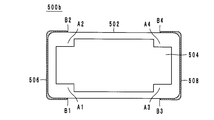
- Patent Document 1 describes a multilayer ceramic capacitor 500b shown in FIG.
- FIG. 8 is a cross-sectional structure diagram of the multilayer ceramic capacitor 500b described in Patent Document 1.
- the same reference numerals are assigned to the same components as those of the multilayer ceramic capacitor 500a.
- the internal electrode 504 has a cross shape as shown in FIG. That is, the notches A 1 to A 4 reach both ends of the internal electrode 504 in the longitudinal direction. As a result, the distance between the internal electrode 504 and the external electrodes 506 and 508 is increased. As a result, even if an electric field distortion occurs in the dielectric ceramic layer sandwiched between the internal electrodes 504, the occurrence of vibrations in the external electrodes 506 and 508 is suppressed. That is, the occurrence of “squeal” is suppressed.
- the cutouts A1 to A4 of the multilayer ceramic capacitor 500b shown in FIG. 8 are larger than the cutouts A1 to A4 of the multilayer ceramic capacitor 500a shown in FIG. For this reason, the capacitance value of the multilayer ceramic capacitor 500b is smaller than the capacitance value of the multilayer ceramic capacitor 500a.
- an object of the present invention is to provide an electronic component that can reduce “squeal” while suppressing a reduction in the capacitance value of the capacitor.
- An electronic component is a multilayer body formed by laminating a plurality of dielectric layers, and has a mounting surface formed by connecting outer edges of the plurality of dielectric layers. And a first capacitor conductor and a second capacitor conductor facing each other by being laminated together with the dielectric layer, wherein the first linear shape parallel to the mounting surface at the outer edge Each of the first linear portion and the second linear portion, and the first lead portion and the second linear portion that are led out from the first linear portion and the second linear portion to the mounting surface, respectively.
- a first capacitor conductor and a second capacitor conductor each having two lead portions, and a surface provided on the mounting surface and adjacent to the mounting surface, the outer edges of the plurality of dielectric layers Is provided on the end face formed in a row
- the second external electrode, and the first linear portion overlaps the second external electrode when viewed in plan from the normal direction of the mounting surface.
- a first recess that is recessed in a direction away from the mounting surface is provided.
- FIG. 1 is a cross-sectional structure diagram of a multilayer ceramic capacitor described in Patent Document 1.
- FIG. 1 is a cross-sectional structure diagram of a multilayer ceramic capacitor described in Patent Document 1.
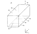
- FIG. 1 is an external perspective view of the electronic component 10.
- FIG. 2 is an exploded perspective view of the multilayer body 12 of the electronic component 10.
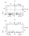
- FIG. 3 is a cross-sectional structure diagram of the electronic component 10.
- the stacking direction of the stacked body 12 is defined as the y-axis direction.
- the long side direction of the laminate 12 when the laminate 12 is viewed in plan from the y-axis direction is defined as the x-axis direction.
- the short side direction of the laminate 12 when the laminate 12 is viewed in plan from the y-axis direction is defined as the z-axis direction.
- the electronic component 10 is a chip capacitor, and includes a laminated body 12, external electrodes 14 (14a, 14b), and a capacitor C (not shown in FIG. 1), as shown in FIGS.
- the laminated body 12 has a rectangular parallelepiped shape. However, the laminated body 12 has a rounded shape at corners and ridgelines by chamfering. In FIG. 2, since the laminated body 12 in a state before chamfering is shown, the corners of the dielectric layer 16 are not rounded.
- a surface on the positive direction side in the y-axis direction is referred to as a side surface S1
- a surface on the negative direction side in the y-axis direction is referred to as a side surface S2.
- the surface on the negative direction side in the x-axis direction is defined as an end surface S3
- the surface on the positive direction side in the x-axis direction is defined as an end surface S4.
- the surface on the positive direction side in the z-axis direction is referred to as an upper surface S5
- the surface on the negative direction side in the z-axis direction is referred to as a lower surface S6.
- the stacked body 12 is configured by stacking a plurality of dielectric layers 16.
- the dielectric layer 16 has a rectangular shape and is made of a dielectric ceramic.
- dielectric ceramics include BaTiO 3 , CaTiO 3 , SrTiO 3 or CaZrO 3 . Further, these materials may be the main components, and Mn compounds, Fe compounds, Cr compounds, Co compounds, or Ni compounds may be subcomponents.
- the thickness of the dielectric layer 16 is preferably 0.5 ⁇ m or more and 10 ⁇ m or less.
- the main surface on the positive side in the y-axis direction of the dielectric layer 16 is referred to as the front surface
- the main surface on the negative direction side in the y-axis direction of the dielectric layer 16 is referred to as the back surface.
- the side surface S1 of the laminate 12 is configured by the surface of the dielectric layer 16 provided on the most positive side in the y-axis direction.
- the side surface S2 of the multilayer body 12 is configured by the back surface of the dielectric layer 16 provided on the most negative direction side in the y-axis direction.
- the end surface S3 is configured by connecting the short sides of the plurality of dielectric layers 16 on the negative direction side in the x-axis direction.
- the end surface S4 is configured by a series of short sides on the positive direction side in the x-axis direction of the plurality of dielectric layers 16.
- the upper surface S5 is configured by the long sides on the positive direction side in the z-axis direction of the plurality of dielectric layers 16 being continuous.
- the lower surface S6 is configured by the long sides on the negative direction side in the z-axis direction of the plurality of dielectric layers 16 being continuous.
- the lower surface S6 is a mounting surface that faces the main surface of the circuit board when the electronic component 10 is mounted on the circuit board.
- the capacitor C is composed of capacitor conductors 18 (18a, 18b) facing each other by being laminated together with the dielectric layer 16.
- the capacitor conductor 18 is made of a conductive material such as Ni, Cu, Ag, Pd, an Ag—Pd alloy, or Au, and has a thickness of 0.3 ⁇ m or more and 2.0 ⁇ m or less. preferable.
- the capacitor conductor 18a is provided on the surface of the dielectric layer 16, and has a capacitance forming portion 20a and a lead portion 22a.
- the capacitance forming portion 20 a has a rectangular shape and does not contact the outer edge of the dielectric layer 16. Since the capacitance forming portion 20a has a rectangular shape, the capacitor conductor 18a has a linear portion L1 parallel to the lower surface S6 at the outer edge, as shown in FIG.
- the linear portion L1 constitutes the long side on the negative direction side in the z-axis direction of the capacitance forming portion 20a, and extends in the x-axis direction.
- the lead portion 22a protrudes from the vicinity of the end portion on the negative direction side in the x-axis direction of the linear portion L1 toward the negative direction side in the z-axis direction, so that the negative direction in the z-axis direction of the dielectric layer 16 It is pulled out to the long side. That is, the drawer portion 22a is pulled out to the lower surface S6.
- a portion where the lead portion 22a is exposed between the two adjacent dielectric layers 16 is referred to as an exposed portion 26a.
- the capacitor conductor 18b is provided on the surface of the dielectric layer 16, and has a capacitance forming portion 20b and a lead portion 22b.
- the capacitance forming portion 20 b has a rectangular shape and does not contact the outer edge of the dielectric layer 16.
- the capacity forming portion 20b overlaps with the capacity forming portion 20a in a state of being substantially coincident when viewed in plan from the y-axis direction. Since the capacitance forming portion 20b has a rectangular shape, the capacitor conductor 18b has a linear portion L2 parallel to the lower surface S6 at the outer edge, as shown in FIG.
- the linear portion L2 constitutes the long side on the negative direction side in the z-axis direction of the capacitance forming portion 20b, and extends in the x-axis direction.
- the lead portion 22b protrudes from the vicinity of the end portion on the positive direction side in the x-axis direction of the linear portion L2 toward the negative direction side in the z-axis direction, so that the negative direction in the z-axis direction of the dielectric layer 16 It is pulled out to the long side. That is, the drawer portion 22b is pulled out to the lower surface S6.
- the lead portion 22b is located closer to the positive direction side in the x-axis direction than the lead portion 22a.
- an exposed portion 26b is referred to as an exposed portion 26b.
- the capacitor conductors 18a and 18b configured as described above are provided on the plurality of dielectric layers 16 so as to be alternately arranged in the y-axis direction.
- the capacitor C is formed in a portion where the capacitor conductor 18a and the capacitor conductor 18b face each other with the dielectric layer 16 therebetween.
- a region where the plurality of dielectric layers 16 provided with the capacitor conductor 18 are stacked is referred to as an inner layer region.
- a plurality of dielectric layers 16 not provided with the capacitor conductor 18 are stacked on the positive side of the inner layer region in the y-axis direction.
- a plurality of dielectric layers 16 not provided with the capacitor conductor 18 are stacked on the negative direction side in the y-axis direction of the inner layer region.
- these two regions where the plurality of dielectric layers 16 where the capacitor conductors 18 are not provided are laminated are referred to as outer layer regions.
- the external electrodes 14a and 14b are formed by direct plating on the lower surface S6 of the laminate 12 so as to cover the exposed portions 26a and 26b, respectively, as shown in FIGS. However, the external electrodes 14a and 14b are not provided on the end surfaces S3 and S4 adjacent to the lower surface S6, respectively.
- the external electrode 14a is located on the negative side in the x-axis direction with respect to the external electrode 14b. Furthermore, as shown in FIG. 3A, the external electrode 14a is provided on the positive direction side in the x-axis direction with respect to the short side on the negative direction side in the x-axis direction of the capacitance forming portion 20a. As shown in FIG.
- the external electrode 14b is provided on the negative direction side in the x-axis direction from the short side of the capacitance forming portion 20b on the positive direction side in the x-axis direction.
- the capacitor C is formed between the external electrode 14a and the external electrode 14b.
- the material of the external electrode 14 include Cu, Ni, and Sn.
- the electronic component 10 has a configuration for reducing “squeal”.
- this configuration will be described in detail.
- the linear portion L1 has a portion overlapping the external electrode 14b when viewed in plan from the z-axis direction (that is, the normal direction of the lower surface S6).
- a recess G1 that is recessed in a direction away from the lower surface S6 is provided.
- the recess G1 has a width that is the same as the width of the lead portion 22b in the x-axis direction, and has a rectangular shape. Thereby, in the recessed part G1, the capacitor
- the linear portion L2 has a portion overlapping the external electrode 14a when viewed in plan from the z-axis direction (that is, the normal direction of the lower surface S6).
- a recess G2 that is recessed in a direction away from the lower surface S6 is provided.
- the recess G2 has a width that is the same as the width of the lead portion 22a in the x-axis direction, and has a rectangular shape. Thereby, in the recessed part G2, the capacitor
- the electronic component 10 as described above is mounted on a circuit board having lands on the main surface. Specifically, the electronic components 10 are mounted on the circuit board by fixing the external electrodes 14a and 14b to the lands with solder.
- BaTiO 3 , CaTiO 3 , SrTiO 3 or CaZrO 3 as main components and Mn compound, Fe compound, Cr compound, Co compound or Ni compound as accessory components are weighed at a predetermined ratio and put into a ball mill.
- Wet preparation The obtained mixture is dried and pulverized, and the obtained powder is calcined.
- the obtained calcined powder is wet pulverized by a ball mill, dried and then crushed to obtain a dielectric ceramic powder.
- the obtained ceramic slurry is formed into a sheet shape on a carrier sheet by a doctor blade method and dried to produce a ceramic green sheet to be the dielectric layer 16.
- the thickness of the ceramic green sheet to be the dielectric layer 16 is preferably 0.5 ⁇ m to 10 ⁇ m.
- capacitor conductors 18a and 18b are formed on the ceramic green sheet to be the dielectric layer 16 by applying a paste made of a conductive material by a screen printing method.
- the paste made of a conductive material is obtained by adding an organic binder and an organic solvent to metal powder such as Ni, for example.
- ceramic green sheets to be the dielectric layer 16 are laminated to obtain an unfired mother laminate. Thereafter, the unfired mother laminate is subjected to pressure bonding with an isostatic press.
- the unfired mother laminate is cut into a predetermined size to obtain a plurality of unfired laminates 12. Then, the surface of the laminate 12 is subjected to barrel polishing to chamfer corners and ridge lines of the laminate 12.
- the firing temperature is preferably 900 ° C. or higher and 1300 ° C. or lower, for example.
- the external electrode 14 composed of three layers of Cu plating, Ni plating, and Sn plating is formed by a plating method.
- the electronic component 10 is completed through the above steps.
- the linear portions L1 and L2 are recessed portions that are recessed in portions overlapping the external electrodes 14b and 14a when viewed in plan from the z-axis direction, respectively.
- G1 and G2 are provided. Accordingly, the capacitor conductor 18a and the capacitor conductor 18b are not opposed to each other in the recesses G1 and G2 adjacent to the external electrodes 14a and 14b. Therefore, even when an AC voltage is applied to the external electrodes 14a and 14b, the electric field-induced distortion is unlikely to occur in the dielectric layer 16 overlapping the recesses G1 and G2.
- the electronic component 10 even when “squeal” is reduced, reduction in the capacitance value of the capacitor C can be suppressed.
- the external electrodes 14a and 14b are provided on the lower surface S6, which is a mounting surface, and are not provided on the end surfaces S3 and S4. Therefore, in the electronic component 10, the width in the x-axis direction of the portion where the external electrodes 14a, 14b and the linear portions L1, L2 face each other is small. Therefore, in the electronic component 10, the width of the recesses G1 and G2 in the x-axis direction can be small. As a result, the reduction in the area of the capacitor conductor 18 due to the provision of the recesses G1 and G2 can be reduced. Therefore, in the electronic component 10, even when “squeal” is reduced, reduction in the capacitance value of the capacitor C can be suppressed.
- the external electrodes 14a and 14b are provided only on the lower surface S6. Therefore, when the electronic component 10 is solder-mounted on the circuit board, fillets are not formed on the side surfaces S1, S2 and the end surfaces S3, S4 of the electronic component 10. Thereby, even if the electronic component 10 vibrates in the z-axis direction, vibration perpendicular to the z-axis direction is not easily transmitted to the circuit board. As a result, “squeal” is reduced in the electronic component 10.
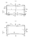
- FIG. 4 is a cross-sectional structure diagram of the electronic component 10a according to the first modification.
- the recesses G1 and G2 were rectangular.
- the recesses G1 and G2 have an arc shape.
- the recesses G1 and G2 have a circular arc shape having a radius r centered on the midpoint of the exposed portion 26a in the x-axis direction.
- "squeal" can be reduced while suppressing a reduction in the capacitance value of the capacitor.
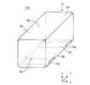
- FIG. 5 is an external perspective view of an electronic component 10b according to a second modification.
- the external electrodes 14a and 14b are provided only on the lower surface S6, and are not provided on the side surfaces S1 and S2 and the end surfaces S3 and S4.
- the external electrodes 14a and 14b are provided on the lower surface S6 and are folded back with respect to the side surfaces S1 and S2. Even when the external electrodes 14a and 14b are folded back to the side surfaces S1 and S2, the width in the x-axis direction of the portion where the external electrodes 14a and 14b and the linear portions L1 and L2 face each other does not change. Therefore, in the electronic component 10 b, as in the electronic component 10, “squeal” can be reduced while suppressing a reduction in the capacitance value of the capacitor C.
- the external electrodes 14a and 14b are folded back to the side surfaces S1 and S2. Therefore, when the electronic component 10b is mounted on the circuit board by soldering, the external electrodes 14a and 14b are provided on the side surfaces S1 and S2. A fillet is formed at the formed portion. As a result, the electronic component 10b is firmly fixed to the circuit board.
- FIG. 6 is a cross-sectional structure diagram of an electronic component 110 according to a comparative example.
- the same components as those of the electronic component 10 are denoted by reference numerals obtained by adding 100 to the reference numerals of the electronic component 10.
- the external electrodes 114a and 114b are provided on the end surfaces S3 and S4, respectively, and are folded back to the side surfaces S1 and S2, the upper surface S5, and the lower surface S6 adjacent to the end surfaces S3 and S4.
- the lead portions 122a and 122b are drawn to the end surfaces S3 and S4, respectively.
- the inventor of the present application has the first to eighteenth samples having the structure of FIG. 3, the nineteenth to twenty-second samples having the structure of FIG. 4, and the twenty-third sample having the structure of FIG. A twenty-fourth sample was produced. Note that the structure shown in FIG. 5 was applied to the external electrode 14 of the fourteenth sample. In the fourteenth sample, the external electrode 14 was folded back on the side surfaces S1, S2 by 100 ⁇ m. Table 1 is a table showing the dimensions of the respective parts of the first to 24th samples.
- a Spacing between the external electrodes 14a, 114a and the external electrodes 14b, 114b b: Spacing between the portions other than the recesses G1, G2 of the sides L1, L2 and the lower surface S6 c: in the x-axis direction of the external electrodes 14, 114 Width d: Thickness e of external electrodes 14 and 114 e: Distance from bottom surface S6 to the bottom of recesses G1 and G2 L: Length of electronic components 10, 10a and 110 in the x-axis direction
- the first sample, the 23rd sample, and the 24th sample whose eb is 0 means that the recesses G1 and G2 are not provided.
- the second sample and the eighth sample in which eb is negative means that the portions where the recesses G1 and G2 are to be provided protrude in the negative direction side in the z-axis direction.
- the number of dielectric layers 16 and 116 was set to 200 to 400.
- the thicknesses of the dielectric layers 16 and 116 were 2 ⁇ m.
- the thickness of the capacitor conductors 18 and 118 was 1 ⁇ m.
- Ni was used as a material for the capacitor conductors 18 and 118.
- Cu was used as the material of the external electrodes 14 and 114.
- the inventor of the present application mounted a sample using Sn—Pd eutectic solder in the center of a circuit board made of glass epoxy resin.
- the size of the circuit board is 100 mm ⁇ 40 mm ⁇ 0.8 mm.
- the inventor applies a voltage obtained by superimposing an AC voltage having an amplitude of 1 V and a frequency of 5 kHz on a DC voltage of 5 V, and converts the sound pressure of the sound generated from the circuit board into a superdirective sound collecting microphone (ALC).
- AAC superdirective sound collecting microphone
- the inventor of the present application also measured the capacitance value of each sample.
- Table 2 is a table showing experimental results.
- the sound pressure is 40 dB or more in the first sample, the second sample, the eighth sample, the 23rd sample, and the 24th sample that are not provided with the recesses G1 and G2.
- the sound pressure is 38 dB or less. Therefore, it can be seen that “squeal” is reduced by providing the recesses G1 and G2.
- the inventor of the present application examined the relationship between e / a and sound pressure in a sample having a sound pressure of 38 dB or less.
- the sound pressure is 38 dB
- the sample where e / a is 0.10 or more The sound pressure is 36 dB or less. Therefore, it is understood that e / a is desirably 0.10 or less.
- the sound pressure is 36 dB, and good results are obtained. Therefore, it can be seen that the external electrode 14 may be folded back to the side surfaces S1 and S2.
- the inventor of the present application conducted a similar experiment by folding the external electrode 14 to the end faces S3 and S4 by 100 ⁇ m, and the sound pressure was 43 dB. Therefore, it is preferable that the external electrode 14 is not folded back at the end surfaces S3 and S4. The reason will be described below.
- eb is preferably 20 ⁇ m or more.
- the present invention is useful for electronic parts, and is particularly excellent in that “squeal” can be reduced while suppressing a reduction in the capacitance value of the capacitor.
Landscapes
- Engineering & Computer Science (AREA)
- Power Engineering (AREA)
- Microelectronics & Electronic Packaging (AREA)
- Manufacturing & Machinery (AREA)
- Chemical & Material Sciences (AREA)
- Materials Engineering (AREA)
- Fixed Capacitors And Capacitor Manufacturing Machines (AREA)
- Ceramic Capacitors (AREA)
Abstract
Description
まず、電子部品の構成について図面を参照しながら説明する。図1は、電子部品10の外観斜視図である。図2は、電子部品10の積層体12の分解斜視図である。図3は、電子部品10の断面構造図である。以下では、積層体12の積層方向をy軸方向と定義する。積層体12をy軸方向から平面視したときの積層体12の長辺方向をx軸方向と定義する。積層体12をy軸方向から平面視したときの積層体12の短辺方向をz軸方向と定義する。
次に、電子部品10の製造方法について説明する。なお、図面は、図1ないし図3を援用する。
以上の電子部品10によれば、「鳴き」を低減できる。より詳細には、図2及び図3に示すように、直線状部L1,L2にはそれぞれ、z軸方向から平面視したときに、外部電極14b,14aと重なっている部分において、窪む凹部G1,G2が設けられている。これにより、外部電極14a,14bと近接する凹部G1,G2において、コンデンサ導体18aとコンデンサ導体18bとは対向していない。したがって、外部電極14a,14bに交流電圧が印加されても、凹部G1,G2と重なる誘電体層16において電界誘起歪みが発生しにくい。その結果、外部電極14a,14bに振動が発生することが抑制され、外部電極14a,14bの振動が回路基板に伝達されることが抑制される。よって、「鳴き」が発生することが抑制される。
次に、第1の変形例に係る電子部品10aについて図面を参照しながら説明する。図4は、第1の変形例に係る電子部品10aの断面構造図である。
次に、第2の変形例に係る電子部品10bについて図面を参照しながら説明する。図5は、第2の変形例に係る電子部品10bの外観斜視図である。
本願発明者は、以上のように構成された電子部品10,10a,10bが奏する効果をより明確にするために、以下に説明する実験を行った。図6は、比較例に係る電子部品110の断面構造図である。電子部品110において、電子部品10と同じ構成については、電子部品10の参照符号に100を足した参照符号を付した。

b:辺L1,L2の凹部G1,G2以外の部分と下面S6との間隔
c:外部電極14,114のx軸方向の幅
d:外部電極14,114の厚み
e:下面S6から凹部G1,G2の底部までの距離
L:電子部品10,10a,110のx軸方向の長さ

S1,S2 側面
S3,S4 端面
S5 上面
S6 下面
10,10a,10b 電子部品
12 積層体
14a,14b 外部電極
16 誘電体層
18a,18b コンデンサ導体
22a,22b 引き出し部
26a,26b 露出部
Claims (4)
- 複数の誘電体層が積層されて構成されてなる積層体であって、該複数の誘電体層の外縁が連なって形成されている実装面を有している積層体と、
前記誘電体層と共に積層されていることにより互いに対向している第1のコンデンサ導体及び第2のコンデンサ導体であって、外縁において前記実装面と平行な第1の直線状部及び第2の直線状部をそれぞれ有していると共に、該第1の直線状部及び該第2の直線状部のそれぞれから該実装面へと引き出されている第1の引き出し部及び第2の引き出し部をそれぞれ有している第1のコンデンサ導体及び第2のコンデンサ導体と、
前記実装面に設けられ、かつ、該実装面に隣接する面であって前記複数の誘電体層の外縁が連なって形成されている端面に設けられていない第1の外部電極及び第2の外部電極であって、前記第1の引き出し部及び前記第2の引き出し部が該実装面に露出している部分をそれぞれ覆っている第1の外部電極及び第2の外部電極と、
を備えており、
前記第1の直線状部には、前記実装面の法線方向から平面視したときに、前記第2の外部電極と重なっている部分において、該実装面から遠ざかる方向に窪む第1の凹部が設けられていること、
を特徴とする電子部品。 - 前記第2の直線状部には、前記第1の引き出し部が引き出されている方向から平面視したときに、前記第1の外部電極と重なっている部分において、前記実装面から遠ざかる方向に窪む第2の凹部が設けられていること、
を特徴とする請求項1に記載の電子部品。 - 前記実装面から前記第1の凹部の底部までの距離を前記第1の外部電極と前記第2の外部電極との間隔で割って得られる値は、0.10以上であること、
を特徴とする請求項1又は請求項2のいずれかに記載の電子部品。 - 前記実装面から前記第1の凹部の底部までの距離は、該実装面から前記第1の直線状部の該第1の凹部以外の部分までの距離よりも20μm以上大きいこと、
を特徴とする請求項1ないし請求項3のいずれかに記載の電子部品。
Priority Applications (4)
| Application Number | Priority Date | Filing Date | Title |
|---|---|---|---|
| KR1020137026318A KR101536678B1 (ko) | 2011-04-07 | 2012-03-07 | 전자부품 |
| JP2013508798A JP5630572B2 (ja) | 2011-04-07 | 2012-03-07 | 電子部品 |
| CN201280016496.0A CN103460318B (zh) | 2011-04-07 | 2012-03-07 | 电子部件 |
| US14/045,863 US9536664B2 (en) | 2011-04-07 | 2013-10-04 | Electronic component |
Applications Claiming Priority (2)
| Application Number | Priority Date | Filing Date | Title |
|---|---|---|---|
| JP2011-085122 | 2011-04-07 | ||
| JP2011085122 | 2011-04-07 |
Related Child Applications (1)
| Application Number | Title | Priority Date | Filing Date |
|---|---|---|---|
| US14/045,863 Continuation US9536664B2 (en) | 2011-04-07 | 2013-10-04 | Electronic component |
Publications (1)
| Publication Number | Publication Date |
|---|---|
| WO2012137569A1 true WO2012137569A1 (ja) | 2012-10-11 |
Family
ID=46968973
Family Applications (1)
| Application Number | Title | Priority Date | Filing Date |
|---|---|---|---|
| PCT/JP2012/055763 Ceased WO2012137569A1 (ja) | 2011-04-07 | 2012-03-07 | 電子部品 |
Country Status (5)
| Country | Link |
|---|---|
| US (1) | US9536664B2 (ja) |
| JP (1) | JP5630572B2 (ja) |
| KR (1) | KR101536678B1 (ja) |
| CN (1) | CN103460318B (ja) |
| WO (1) | WO2012137569A1 (ja) |
Cited By (7)
| Publication number | Priority date | Publication date | Assignee | Title |
|---|---|---|---|---|
| JP2014096552A (ja) * | 2012-11-07 | 2014-05-22 | Samsung Electro-Mechanics Co Ltd | 積層セラミック電子部品及びその実装基板 |
| JP2014120748A (ja) * | 2012-12-18 | 2014-06-30 | Samsung Electro-Mechanics Co Ltd | 積層セラミックキャパシタ及び積層セラミックキャパシタが実装された回路基板 |
| KR20140113453A (ko) * | 2013-03-15 | 2014-09-24 | 가부시키가이샤 무라타 세이사쿠쇼 | 적층 콘덴서 |
| CN104240945A (zh) * | 2013-06-14 | 2014-12-24 | 三星电机株式会社 | 多层陶瓷电容器及其上安装有该多层陶瓷电容器的板 |
| JP2015176998A (ja) * | 2014-03-14 | 2015-10-05 | 京セラ株式会社 | 電子部品の実装構造 |
| US10522290B2 (en) | 2015-12-03 | 2019-12-31 | Murata Manufacturing Co., Ltd. | Multilayer ceramic electronic component |
| JP2023099414A (ja) * | 2021-12-31 | 2023-07-13 | サムソン エレクトロ-メカニックス カンパニーリミテッド. | 積層型キャパシタ |
Families Citing this family (3)
| Publication number | Priority date | Publication date | Assignee | Title |
|---|---|---|---|---|
| US9865400B2 (en) * | 2015-07-15 | 2018-01-09 | Murata Manufacturing Co., Ltd. | Capacitor |
| US10414358B2 (en) * | 2016-02-03 | 2019-09-17 | The Boeing Company | Composite panel power system |
| WO2018093626A1 (en) * | 2016-11-15 | 2018-05-24 | Kemet Electronics Corporation | Face down mlcc |
Citations (2)
| Publication number | Priority date | Publication date | Assignee | Title |
|---|---|---|---|---|
| JPH0945830A (ja) * | 1995-08-03 | 1997-02-14 | Murata Mfg Co Ltd | チップ状電子部品 |
| JP2009054973A (ja) * | 2007-08-29 | 2009-03-12 | Kyocera Corp | 積層コンデンサおよびコンデンサ実装基板 |
Family Cites Families (9)
| Publication number | Priority date | Publication date | Assignee | Title |
|---|---|---|---|---|
| JPH0669063A (ja) * | 1992-08-12 | 1994-03-11 | Murata Mfg Co Ltd | 積層コンデンサ |
| JPH06283385A (ja) * | 1993-03-30 | 1994-10-07 | Taiyo Yuden Co Ltd | チップ型コンデンサアレイ |
| US6950300B2 (en) * | 2003-05-06 | 2005-09-27 | Marvell World Trade Ltd. | Ultra low inductance multi layer ceramic capacitor |
| US7329976B2 (en) * | 2005-04-27 | 2008-02-12 | Kyocera Corporation | Laminated electronic component |
| WO2007020757A1 (ja) * | 2005-08-19 | 2007-02-22 | Murata Manufacturing Co., Ltd. | 積層セラミックコンデンサ |
| JP4925958B2 (ja) * | 2007-07-27 | 2012-05-09 | 京セラ株式会社 | 積層セラミックコンデンサ |
| JP4953989B2 (ja) * | 2007-08-29 | 2012-06-13 | 京セラ株式会社 | 積層コンデンサおよびコンデンサ実装基板 |
| JP5035318B2 (ja) * | 2009-10-23 | 2012-09-26 | Tdk株式会社 | 積層型コンデンサ |
| JP5035319B2 (ja) * | 2009-10-23 | 2012-09-26 | Tdk株式会社 | 積層型コンデンサ |
-
2012
- 2012-03-07 KR KR1020137026318A patent/KR101536678B1/ko active Active
- 2012-03-07 JP JP2013508798A patent/JP5630572B2/ja active Active
- 2012-03-07 CN CN201280016496.0A patent/CN103460318B/zh active Active
- 2012-03-07 WO PCT/JP2012/055763 patent/WO2012137569A1/ja not_active Ceased
-
2013
- 2013-10-04 US US14/045,863 patent/US9536664B2/en active Active
Patent Citations (2)
| Publication number | Priority date | Publication date | Assignee | Title |
|---|---|---|---|---|
| JPH0945830A (ja) * | 1995-08-03 | 1997-02-14 | Murata Mfg Co Ltd | チップ状電子部品 |
| JP2009054973A (ja) * | 2007-08-29 | 2009-03-12 | Kyocera Corp | 積層コンデンサおよびコンデンサ実装基板 |
Cited By (11)
| Publication number | Priority date | Publication date | Assignee | Title |
|---|---|---|---|---|
| JP2014096552A (ja) * | 2012-11-07 | 2014-05-22 | Samsung Electro-Mechanics Co Ltd | 積層セラミック電子部品及びその実装基板 |
| US9214278B2 (en) | 2012-11-07 | 2015-12-15 | Samsung Electro-Mechanics Co., Ltd. | Multilayered ceramic electronic component and board for mounting the same |
| JP2014120748A (ja) * | 2012-12-18 | 2014-06-30 | Samsung Electro-Mechanics Co Ltd | 積層セラミックキャパシタ及び積層セラミックキャパシタが実装された回路基板 |
| KR20140113453A (ko) * | 2013-03-15 | 2014-09-24 | 가부시키가이샤 무라타 세이사쿠쇼 | 적층 콘덴서 |
| KR101601822B1 (ko) * | 2013-03-15 | 2016-03-09 | 가부시키가이샤 무라타 세이사쿠쇼 | 적층 콘덴서 |
| CN104240945A (zh) * | 2013-06-14 | 2014-12-24 | 三星电机株式会社 | 多层陶瓷电容器及其上安装有该多层陶瓷电容器的板 |
| KR102057909B1 (ko) * | 2013-06-14 | 2019-12-20 | 삼성전기주식회사 | 적층 세라믹 커패시터 및 적층 세라믹 커패시터의 실장 기판 |
| JP2015176998A (ja) * | 2014-03-14 | 2015-10-05 | 京セラ株式会社 | 電子部品の実装構造 |
| US10522290B2 (en) | 2015-12-03 | 2019-12-31 | Murata Manufacturing Co., Ltd. | Multilayer ceramic electronic component |
| JP2023099414A (ja) * | 2021-12-31 | 2023-07-13 | サムソン エレクトロ-メカニックス カンパニーリミテッド. | 積層型キャパシタ |
| JP7835498B2 (ja) | 2021-12-31 | 2026-03-25 | サムソン エレクトロ-メカニックス カンパニーリミテッド. | 積層型キャパシタ |
Also Published As
| Publication number | Publication date |
|---|---|
| CN103460318A (zh) | 2013-12-18 |
| KR101536678B1 (ko) | 2015-07-14 |
| KR20130135936A (ko) | 2013-12-11 |
| JPWO2012137569A1 (ja) | 2014-07-28 |
| CN103460318B (zh) | 2016-10-12 |
| US20140029158A1 (en) | 2014-01-30 |
| US9536664B2 (en) | 2017-01-03 |
| JP5630572B2 (ja) | 2014-11-26 |
Similar Documents
| Publication | Publication Date | Title |
|---|---|---|
| JP5630572B2 (ja) | 電子部品 | |
| JP5810706B2 (ja) | 電子部品 | |
| JP5884653B2 (ja) | 実装構造 | |
| JP5899699B2 (ja) | 積層型コンデンサ | |
| JP2011238724A (ja) | 電子部品 | |
| CN108155006B (zh) | 电子部件 | |
| JP2020057738A (ja) | 電子部品、回路基板、および電子部品の回路基板への実装方法 | |
| US9653214B2 (en) | Laminated capacitor and laminated capacitor series and laminated capacitor mounted body including capacitor | |
| JP6466690B2 (ja) | 積層型コンデンサ | |
| JPWO2011071145A1 (ja) | 積層型セラミックコンデンサ | |
| JP2018067562A (ja) | 積層セラミックコンデンサおよびその実装構造体 | |
| JP2011233840A (ja) | 電子部品 | |
| JP5605342B2 (ja) | 電子部品及び基板モジュール | |
| JP2016034047A (ja) | 実装構造 | |
| JP5201223B2 (ja) | 電子部品及び基板モジュール | |
| KR101418453B1 (ko) | 적층 콘덴서 | |
| KR20190116116A (ko) | 적층 세라믹 전자부품 | |
| KR101405829B1 (ko) | 전자부품 및 선택방법 | |
| KR20140145829A (ko) | 적층 세라믹 커패시터 및 적층 세라믹 커패시터의 실장 기판 | |
| JP2009059888A (ja) | 積層セラミックコンデンサ | |
| JP5652487B2 (ja) | 積層セラミックコンデンサ | |
| JP5915800B2 (ja) | 電子部品 | |
| JP2022114628A (ja) | 積層コンデンサ | |
| JP2014187381A (ja) | 電子部品及び実装構造体 | |
| JP2011176359A (ja) | 積層型コンデンサの実装構造 |
Legal Events
| Date | Code | Title | Description |
|---|---|---|---|
| 121 | Ep: the epo has been informed by wipo that ep was designated in this application |
Ref document number: 12767401 Country of ref document: EP Kind code of ref document: A1 |
|
| ENP | Entry into the national phase |
Ref document number: 2013508798 Country of ref document: JP Kind code of ref document: A |
|
| ENP | Entry into the national phase |
Ref document number: 20137026318 Country of ref document: KR Kind code of ref document: A |
|
| NENP | Non-entry into the national phase |
Ref country code: DE |
|
| 122 | Ep: pct application non-entry in european phase |
Ref document number: 12767401 Country of ref document: EP Kind code of ref document: A1 |