WO2012132655A1 - 裏面接合型の光電変換素子及び裏面接合型の光電変換素子の製造方法 - Google Patents
裏面接合型の光電変換素子及び裏面接合型の光電変換素子の製造方法 Download PDFInfo
- Publication number
- WO2012132655A1 WO2012132655A1 PCT/JP2012/054233 JP2012054233W WO2012132655A1 WO 2012132655 A1 WO2012132655 A1 WO 2012132655A1 JP 2012054233 W JP2012054233 W JP 2012054233W WO 2012132655 A1 WO2012132655 A1 WO 2012132655A1
- Authority
- WO
- WIPO (PCT)
- Prior art keywords
- insulating layer
- layer
- amorphous semiconductor
- photoelectric conversion
- semiconductor layer
- Prior art date
- Legal status (The legal status is an assumption and is not a legal conclusion. Google has not performed a legal analysis and makes no representation as to the accuracy of the status listed.)
- Ceased
Links
Images








Classifications
-
- H—ELECTRICITY
- H10—SEMICONDUCTOR DEVICES; ELECTRIC SOLID-STATE DEVICES NOT OTHERWISE PROVIDED FOR
- H10F—INORGANIC SEMICONDUCTOR DEVICES SENSITIVE TO INFRARED RADIATION, LIGHT, ELECTROMAGNETIC RADIATION OF SHORTER WAVELENGTH OR CORPUSCULAR RADIATION
- H10F77/00—Constructional details of devices covered by this subclass
- H10F77/20—Electrodes
- H10F77/206—Electrodes for devices having potential barriers
- H10F77/211—Electrodes for devices having potential barriers for photovoltaic cells
- H10F77/219—Arrangements for electrodes of back-contact photovoltaic cells
-
- H—ELECTRICITY
- H10—SEMICONDUCTOR DEVICES; ELECTRIC SOLID-STATE DEVICES NOT OTHERWISE PROVIDED FOR
- H10F—INORGANIC SEMICONDUCTOR DEVICES SENSITIVE TO INFRARED RADIATION, LIGHT, ELECTROMAGNETIC RADIATION OF SHORTER WAVELENGTH OR CORPUSCULAR RADIATION
- H10F10/00—Individual photovoltaic cells, e.g. solar cells
- H10F10/10—Individual photovoltaic cells, e.g. solar cells having potential barriers
- H10F10/16—Photovoltaic cells having only PN heterojunction potential barriers
- H10F10/164—Photovoltaic cells having only PN heterojunction potential barriers comprising heterojunctions with Group IV materials, e.g. ITO/Si or GaAs/SiGe photovoltaic cells
- H10F10/165—Photovoltaic cells having only PN heterojunction potential barriers comprising heterojunctions with Group IV materials, e.g. ITO/Si or GaAs/SiGe photovoltaic cells the heterojunctions being Group IV-IV heterojunctions, e.g. Si/Ge, SiGe/Si or Si/SiC photovoltaic cells
- H10F10/166—Photovoltaic cells having only PN heterojunction potential barriers comprising heterojunctions with Group IV materials, e.g. ITO/Si or GaAs/SiGe photovoltaic cells the heterojunctions being Group IV-IV heterojunctions, e.g. Si/Ge, SiGe/Si or Si/SiC photovoltaic cells the Group IV-IV heterojunctions being heterojunctions of crystalline and amorphous materials, e.g. silicon heterojunction [SHJ] photovoltaic cells
-
- H—ELECTRICITY
- H10—SEMICONDUCTOR DEVICES; ELECTRIC SOLID-STATE DEVICES NOT OTHERWISE PROVIDED FOR
- H10F—INORGANIC SEMICONDUCTOR DEVICES SENSITIVE TO INFRARED RADIATION, LIGHT, ELECTROMAGNETIC RADIATION OF SHORTER WAVELENGTH OR CORPUSCULAR RADIATION
- H10F71/00—Manufacture or treatment of devices covered by this subclass
- H10F71/121—The active layers comprising only Group IV materials
-
- Y—GENERAL TAGGING OF NEW TECHNOLOGICAL DEVELOPMENTS; GENERAL TAGGING OF CROSS-SECTIONAL TECHNOLOGIES SPANNING OVER SEVERAL SECTIONS OF THE IPC; TECHNICAL SUBJECTS COVERED BY FORMER USPC CROSS-REFERENCE ART COLLECTIONS [XRACs] AND DIGESTS
- Y02—TECHNOLOGIES OR APPLICATIONS FOR MITIGATION OR ADAPTATION AGAINST CLIMATE CHANGE
- Y02E—REDUCTION OF GREENHOUSE GAS [GHG] EMISSIONS, RELATED TO ENERGY GENERATION, TRANSMISSION OR DISTRIBUTION
- Y02E10/00—Energy generation through renewable energy sources
- Y02E10/50—Photovoltaic [PV] energy
- Y02E10/547—Monocrystalline silicon PV cells
-
- Y—GENERAL TAGGING OF NEW TECHNOLOGICAL DEVELOPMENTS; GENERAL TAGGING OF CROSS-SECTIONAL TECHNOLOGIES SPANNING OVER SEVERAL SECTIONS OF THE IPC; TECHNICAL SUBJECTS COVERED BY FORMER USPC CROSS-REFERENCE ART COLLECTIONS [XRACs] AND DIGESTS
- Y02—TECHNOLOGIES OR APPLICATIONS FOR MITIGATION OR ADAPTATION AGAINST CLIMATE CHANGE
- Y02P—CLIMATE CHANGE MITIGATION TECHNOLOGIES IN THE PRODUCTION OR PROCESSING OF GOODS
- Y02P70/00—Climate change mitigation technologies in the production process for final industrial or consumer products
- Y02P70/50—Manufacturing or production processes characterised by the final manufactured product
Definitions
- the present invention relates to a back junction photoelectric conversion element and a method for manufacturing a back junction photoelectric conversion element, and in particular, a back surface that uses an insulating layer to separately form a p-type region and an n-type region for forming the photoelectric conversion element.
- the present invention relates to a method for manufacturing a junction type photoelectric conversion element and a back surface junction type photoelectric conversion element.
- a solar cell is also called a photovoltaic device or a photoelectric conversion element, but is expected as a clean energy source, and various structures are used to improve photoelectric conversion efficiency.
- Patent Document 1 discloses a configuration in which i-type amorphous silicon and p-type amorphous silicon are stacked on n-type single crystal silicon as a photovoltaic device having a heterojunction.
- a solar cell is formed across a pair of second semiconductor layers disposed on both sides of the first semiconductor layer and from one of the second semiconductor layers to the first semiconductor layer.
- the structure provided with the insulating layer and the insulating layer formed ranging over the 1st semiconductor layer from the other 2nd semiconductor layer is disclosed.
- the transparent electrode layer and the collecting electrode layer are separated into an electrode for the first semiconductor layer and an electrode for the second semiconductor layer by a pair of separation grooves formed on the insulating layer.
- the solar cell described in Patent Document 2 is provided with an electrode for the first semiconductor layer and an electrode for the second semiconductor layer on the back surface opposite to the light receiving surface.
- Such a structure is called a back junction type photoelectric conversion element, and since no electrode is arranged on the light receiving surface, a large light receiving area can be obtained and the photoelectric conversion efficiency can be improved.
- an insulating layer is used to make a p type region and an n type region separately.
- the electrode opens this insulating layer and is connected to the p-type region or the n-type region.
- a residue of the insulating layer may remain in the opening process. This hinders the improvement of conversion efficiency.
- An object of the present invention is to provide a back junction type photoelectric conversion element and a method for producing a back junction type photoelectric conversion element that can reliably remove residues at the time of opening an insulating layer and ensure improvement in conversion efficiency. It is.
- the back junction type photoelectric conversion element includes a first conductivity type semiconductor substrate having a light receiving surface and a back surface opposite to the light receiving surface, and is disposed on the back surface and connected to the semiconductor substrate.
- a first conductivity type region configured to include an amorphous semiconductor layer having a semiconductor layer, and an amorphous semiconductor layer disposed on the back surface and having a second conductivity type to form a pn junction with the semiconductor substrate.
- the insulating layer formed on the amorphous semiconductor layer in either the first conductive type region or the second conductive type region, and the opening provided in the insulating layer An electrode layer connected to an amorphous semiconductor layer provided under the electrode layer and drawn to the outside, and the insulating layer includes a first insulating layer provided in contact with the amorphous semiconductor layer provided under the electrode layer; A second insulating layer formed on the first insulating layer, wherein the first insulating layer In forming the opening, characterized in that it comprises a second insulating layer having a film quality to be removed by a lift-off, the.
- the manufacturing method of the back junction type photoelectric conversion element according to the present invention is a manufacturing method of a back junction type photoelectric conversion element in which a pn junction is formed on the back surface opposite to the light receiving surface of the first conductivity type silicon substrate.
- the step of opening the second insulating layer, the etching rate with respect to the first insulating layer is faster than the etching rate with respect to the second insulating layer, and the non-insulating layer provided below the insulating layer than the etching rate with respect to the first insulating layer.
- the insulating layer is formed on the first insulating layer and the first insulating layer provided in contact with the amorphous semiconductor layer provided therebelow. And a second insulating layer having a film quality that is removed by lift-off when the opening of the first insulating layer is formed.
- the first insulating layer residues at the time of opening the second insulating layer can be reliably removed by lift-off.
- FIG. 10 it is a figure explaining a mode that lift-off is performed. It is a figure which shows a mode that a resist is removed after the process of FIG. It is a figure which shows the mode of S40 of FIG. It is a figure which shows the mode of S42 of FIG. It is a figure which shows the mode of S44 of FIG. It is a figure which shows the mode of S46 of FIG. It is sectional drawing of the back junction type photoelectric conversion element as a comparative example. It is a flowchart which shows the procedure of the manufacturing method of the back junction type photoelectric conversion element as a comparative example. It is a figure which shows the mode of S10 in a comparative example. It is a figure which shows the mode of S12 in a comparative example.
- the conductivity type of the semiconductor substrate is described as n-type, but it may be p-type. Further, the order of formation of the amorphous semiconductor layers is n-type first and p-type thereafter, but this may be interchanged.
- the opening of the insulating layer for the contact is provided at the n-type amorphous semiconductor layer, it may be provided at the p-type amorphous semiconductor layer.
- an i-type amorphous semiconductor layer is used in addition to the p-type amorphous semiconductor layer and the n-type amorphous semiconductor layer. Therefore, even if an i-type amorphous semiconductor layer is included between pn junctions, it belongs to the pn junction.
- the insulating layer has a two-layer structure of SiO 2 and SiN x , but it may have a multilayer structure of two or more layers.
- SiN x may have a laminated structure of silicon nitride films having different film qualities.
- the materials, film thicknesses, and the like described below are exemplifications for explanation, and can be appropriately changed according to the specifications of the back junction photoelectric conversion element.
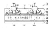
- FIG. 1 is a cross-sectional view of a back contact type photoelectric conversion element 10.
- the back junction type photoelectric conversion element 10 a pn junction for performing photoelectric conversion is formed on the back surface opposite to the light receiving surface, and electrodes are provided only on the back surface.
- the lower side of the paper is the light-receiving surface side
- the upper side is the back surface.
- the back junction type photoelectric conversion element 10 is simply referred to as the photoelectric conversion element 10.
- the photoelectric conversion element 10 is provided with an n-type region 100 and a p-type region 102 on the back surface of a semiconductor substrate 20 which is an n-type silicon single crystal substrate.
- the n-type region 100 is connected to the semiconductor substrate 20 and includes an n-type amorphous semiconductor layer 28 having the same conductivity type.
- the i-type amorphous semiconductor layer 24 is provided between the semiconductor substrate 20 and the n-type amorphous semiconductor layer 28, but the i-type amorphous semiconductor layer 24 is not necessarily an essential component.
- the p-type region 102 includes a p-type amorphous semiconductor layer 44 and forms a pn junction with the semiconductor substrate 20.
- an i-type amorphous semiconductor layer 42 is provided between the semiconductor substrate 20 and the p-type amorphous semiconductor layer 44, but the i-type amorphous semiconductor layer 42 is not necessarily an essential component. .
- the n-type region electrode 70 is a plating electrode connected to the n-type amorphous semiconductor layer 28.
- the electrode 70 has a laminated structure of Sn and Cu.
- the base electrodes 60 and 62 provided between the n-type region electrode 70 and the n-type amorphous semiconductor layer 28 are seed layers used when the electrode 70 is plated.
- the base electrodes 60 and 62 have a laminated structure of a transparent electrode layer 60 and a Cu layer 62.
- the electrode 72 for the p-type region is a plating electrode connected to the p-type amorphous semiconductor layer 44. Similar to the electrode 70, the electrode 72 has a laminated structure of Sn and Cu, and is formed by plating using the base electrodes 60 and 62. Comparing the n-type region electrode 70 and the p-type region electrode 72, the former electrode height is higher than the latter electrode height. This is because the surface area of the former base electrodes 60 and 62 is set smaller than the surface area of the latter base electrodes 60 and 62. That is, when plating is performed using the base electrodes 60 and 62 in common, the plating current density varies depending on the surface area difference, and the smaller surface area grows faster.
- the electrode 72 for the p-type region is provided directly on the p-type amorphous semiconductor layer 44 via the base electrodes 60 and 62.
- the electrode 70 for the n-type region is provided with an opening in an insulating layer having a laminated structure of the silicon oxide layer 36 and the silicon nitride layer 40, and through the opening through the base electrodes 60 and 62, the n-type region It is connected to the amorphous semiconductor layer 28.
- the photoelectric conversion element 10 is characterized in that the insulating layer has a laminated structure of a silicon oxide layer 36 and a silicon nitride layer 40.
- the thickness of the silicon nitride layer 40 is about 10 nm to 500 nm, but the thickness of the silicon oxide layer 36 is thicker than the thickness of the natural oxide film, and may be about several nm to 200 nm.
- the i-type amorphous semiconductor layer 22 and the n-type amorphous semiconductor layer 26 provided on the light receiving surface of the semiconductor substrate 20 are layers having a function as a passivation layer of the semiconductor substrate 20 on which photoelectric conversion is performed.
- the antireflection layer 38 is an insulating film layer having a function of suppressing reflection on the light receiving surface.
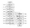
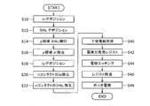
- FIG. 2 is a flowchart showing a manufacturing procedure of the photoelectric conversion element 10. This procedure will be described with reference to FIGS.
- a semiconductor substrate 20 which is an n-type silicon single crystal substrate is prepared.
- the plane direction is preferably (100).
- the surface serving as the light receiving surface has a texture structure. For example, pyramidal irregularities surrounded by the (111) plane can be provided on the surface by utilizing the plane anisotropy of silicon etching.
- the semiconductor substrate 20 is entirely cleaned with an appropriate cleaning solution for the next step.
- the i-type amorphous semiconductor layer and the n-type amorphous semiconductor layer are sequentially deposited on the semiconductor substrate 20 having a clean surface (S10).
- Deposition is also called deposition and is a process of forming a thin film. This step can be performed using a plasma CVD apparatus.
- the i-type amorphous semiconductor layer and the n-type amorphous semiconductor layer are both formed on the front surface and the back surface of the semiconductor substrate 20.
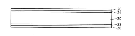
- an i-type amorphous semiconductor layer 22 and an n-type amorphous semiconductor layer 26 are formed on the front surface, and an i-type amorphous semiconductor layer 24 and an n-type amorphous semiconductor layer 28 are formed on the back surface. Is shown.
- a silicon oxide layer is deposited on the back surface (S11).
- a representative example of silicon oxide is SiO 2 .
- This step is performed using a plasma CVD apparatus. Since the natural oxide film has a thickness of 1 nm or less, the thickness of the silicon oxide layer is preferably about several nm to 200 nm thicker than this.
- One of the roles of providing the silicon oxide layer is to protect the surface of the n-type amorphous semiconductor layer 24, thereby improving the photoelectric conversion efficiency. Another role is that it is easily dissolved in HF (hydrofluoric acid). Therefore, in the insulating film opening process described later, the SiN x residue is removed by lift-off, and the surface of the clean n-type amorphous semiconductor layer 24 is removed. It is to be.
- the characteristic of the photoelectric conversion element 10 is that SiO 2 is provided.
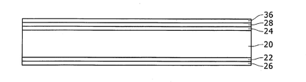
- FIG. 4 shows how the silicon oxide layer 36 is formed on the n-type amorphous semiconductor layer 28 on the back surface.
- the silicon nitride layer is deposited (S12). This process is also performed using a plasma CVD apparatus.
- a typical example of silicon nitride is Si 3 N 4 , but the composition of Si 3 N 4 does not necessarily depend on the manufacturing conditions of the plasma CVD apparatus. Generally, the composition is SiN x .
- the thickness of the silicon nitride layer 40 is about 10 nm to 500 nm.
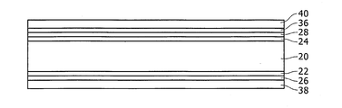
- FIG. 5 shows a state in which the silicon nitride layer 40 is formed on the silicon oxide layer 36 on the back surface.
- An antireflection layer 38 is formed on the surface that becomes the light receiving surface. Since a silicon nitride film can be used as the antireflection layer 38, the same film as the silicon nitride layer 40 on the back surface may be formed on the light receiving surface side at the same time. However, the silicon nitride layer 40 on the back surface is used for subsequent patterning and etching characteristics are important, whereas the antireflection layer 38 has optical characteristics important. Therefore, the back side silicon nitride layer 40 and the antireflection layer 38 are preferably insulating films having different film characteristics. In the following, the description will be made while distinguishing the silicon nitride layer 40 on the back surface and the antireflection layer 38 on the light receiving surface side.
- the silicon nitride layer 40 on the back surface can be formed by changing the film composition, for example, so that the etching characteristics can be distinguished from those having alkali resistance and those having acid resistance.
- the silicon oxide layer 36 side can be formed as an acid-resistant film, and an alkali-resistant film can be formed thereon.
- the silicon nitride layer in contact with the resist film is preferably resistant to alkali.
- the silicon nitride layer 40 is partially removed (S14).
- a photolithography technique is used for this processing. That is, a photosensitive resist film is applied to the entire surface of the silicon nitride layer 40, the resist film in a portion where the silicon nitride layer 40 is to be removed is exposed, and the resist film in that portion is removed by development. This process is patterning of the resist film. Then, using the resist film as an etching mask, a portion of the silicon nitride layer 40 without the resist film is removed using an appropriate etching solution. As the etchant, hydrofluoric acid which is a mixture of HF and nitric acid can be used. After the etching, washing with water is performed.
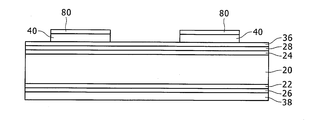
- FIG. 6 shows the patterned resist film 80 and the remaining silicon nitride layer 40 using the resist film 80 as an etching mask. Thereafter, the resist film 80 is removed. Since the resist film 80 is soluble in alkali, only the resist film 80 can be removed using caustic soda (NaOH) while leaving the silicon nitride layer 40 as it is.
- CaOH caustic soda
- the n-type amorphous semiconductor layer 28 and the i-type amorphous semiconductor layer 24 thereunder are formed using the silicon nitride layer 40 as an etching mask. It is removed (S16).
- caustic soda (NaOH) is used by utilizing the fact that the amorphous semiconductor layer dissolves in alkali.
- the treatment is performed in the order of organic cleaning, caustic soda, SC2 which is a mixed solution of hydrochloric acid (HCl) and hydrogen peroxide (H 2 O 2 ), hydrofluoric acid, and water washing.
- the hydrofluoric acid is used to remove the oxide film formed by SC2.
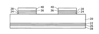
- the silicon oxide layer 36, the n-type amorphous semiconductor layer 28, and the i-type amorphous semiconductor layer 24 are left in the shape of the silicon nitride layer 40, and the semiconductor substrate 20 is exposed in other portions. The situation is shown. In this way, opening of the portion of the p-type region 102 is performed.
- the i-type amorphous semiconductor layer 42 and the p-type amorphous semiconductor layer 44 are deposited on the entire surface (S18). This step is performed using a plasma CVD apparatus.
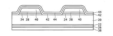
- the i-type amorphous semiconductor layer 42 and the p-type amorphous semiconductor layer 44 are in contact with the semiconductor substrate 20 which is an n-type silicon single crystal substrate in the opened p-type region 102. Is shown. Note that an i-type amorphous semiconductor layer 42 and a p-type amorphous semiconductor layer 44 are also deposited on the silicon nitride layer 40.
- an opening process for contacting the electrode with the n-type amorphous semiconductor layer 28 is performed.
- a contact is an electrical connection.
- a silicon oxide layer 36, a silicon nitride layer 40, an i-type amorphous semiconductor layer 42, and a p-type amorphous semiconductor layer 44 are present on the n-type amorphous semiconductor layer 28. Therefore, a process for removing them in order is performed.
- the p-type amorphous semiconductor layer 44 and the i-type amorphous semiconductor layer 42 are removed (S20).
- a photolithography technique is used for this processing. That is, a resist film is applied, and the applied resist film is patterned to remove the n-contact portion by exposure and development. A solvent-soluble type having acid resistance and alkali resistance is used for the resist film.
- the p-type amorphous semiconductor layer 44 and the i-type amorphous semiconductor layer 42 can be removed using caustic soda (NaOH). Thereafter, cleaning is performed.
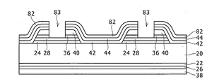
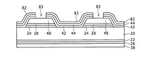
- FIG. 9 shows a state where the p-type amorphous semiconductor layer 44 and the i-type amorphous semiconductor layer 42 in the opening 83 portion of the resist film 82 are removed.
- the silicon nitride layer 40 is removed (S22) and the silicon oxide layer 36 is removed (S23).
- hydrofluoric acid is used. Although hydrofluoric acid can etch both the silicon nitride layer 40 and the silicon oxide layer 36, the etching rate for the silicon oxide layer 36 is considerably faster than the etching rate for the silicon nitride layer 40. Further, the etching rate for the p-type amorphous semiconductor layer 28 is slower than the etching rate for the silicon oxide layer 36.
- the silicon nitride layer 40 is first etched, and when the silicon oxide layer 36 is reached, the silicon oxide layer 36 is rapidly etched, but when the p-type amorphous semiconductor layer 28 is reached, the etching is performed. Stop.
- a protective film is preferably provided so that the antireflection layer 38 on the light receiving surface side is not etched.
- silicon nitride formed by plasma CVD can be removed by hydrofluoric acid, in practice, a minute residue remains, and it may take a considerable time to completely remove the residue.
- silicon nitride formed by a plasma CVD apparatus may not have a stoichiometric composition of Si 3 N 4 but may have an excessively large Si composition such as Si 3.5 N 4. Conceivable.
- electrical contact between the electrode and the n-type amorphous semiconductor layer 28 is hindered, and the photoelectric conversion efficiency of the photoelectric conversion element 10 is reduced. Become.
- the silicon oxide layer 36 when the silicon oxide layer 36 is disposed between the silicon nitride layer 40 and the n-type amorphous semiconductor layer 28, the silicon oxide layer 36 can be easily removed using hydrofluoric acid. At this time, even if there is a residue of the silicon nitride layer 40 on the silicon oxide layer 36, the silicon nitride on the silicon oxide layer 36 is removed by a so-called lift-off phenomenon.
- the silicon oxide layer 36 and hydrofluoric acid are used to remove the silicon nitride layer 40 by lift-off.
- an intermediate film that can remove the residue of the insulating layer by lift-off and a remover for the intermediate film Can be used in combination.
- FIG. 10 shows a state in which the silicon nitride layer 40 and the silicon oxide layer 36 are removed while leaving the resist film 82, and an opening 83 for contact with the n-type amorphous semiconductor layer 28 is formed. .
- FIG. 11 is a diagram schematically showing how the silicon nitride residue 41 on the silicon oxide layer 36 is removed by the lift-off phenomenon.
- hydrofluoric acid indicated as HF can reach the silicon oxide layer 36 through the gaps between the silicon nitride residues 41 and dissolve the silicon oxide layer 36.
- the silicon oxide layer 36 is dissolved, the silicon nitride residue 41 is floated and separated from the silicon oxide layer 36.
- the silicon nitride residue 41 is removed together with the removal of the silicon oxide layer 36.
- FIG. 11 is a view showing a state where the resist film 82 has been removed.
- the base electrode is a conductive seed layer for forming a plating electrode.
- a transparent electrode layer called a TCO (Transparent Conductive Oxide) layer is formed over the entire surface, and a Cu layer is formed over the entire surface.
- TCO Transparent Conductive Oxide
- the light-transmitting conductive layer indium tin oxide or the like can be used.
- the thickness of the TCO layer which is a transparent electrode layer, is about 100 nm, and the thickness of the Cu layer is about 100 nm to 1 ⁇ m.
- This step is processed using a sputtering apparatus.
- FIG. 13 shows a state in which a laminated structure of the transparent electrode layer 60 and the Cu layer 62 is formed on the entire surface as the base electrodes 60 and 62.
- a resist film for electrode separation is formed (S42). This is because the n-type region electrode 70 and the p-type region electrode 72 are electrically separated and plated.
- a resist film is applied, and patterning is performed by exposure and development to form a separation groove at the boundary between the n-type region portion and the p-type region portion.
- FIG. 14 shows a resist film 84 in which a separation groove 85 is formed.
- FIG. 15 shows a state in which the base electrodes 60 and 62 at the separation groove 85 are removed by this etching.
- FIG. 16 shows a state in which the resist film is removed, and the base electrodes 60 and 62 are separated into the n-type region 100 and the p-type region 102 by the separation unit 86.
- a plating electrode is formed (S48). Specifically, cleaning with sulfuric acid (H 2 SO 4 ), electrolytic plating of Cu using a plating bath and subsequent cleaning, electrolytic plating of Sn using a plating bath, and subsequent cleaning are sequentially performed.
- the thickness of the Cu plating layer is about 10 ⁇ m to 20 ⁇ m, and the thickness of the Sn plating layer is 1 ⁇ m to 5 ⁇ m. In this way, the photoelectric conversion element 10 having the structure described in FIG. 1 is completed.
- FIG. 17 corresponds to FIG. 1 and is a cross-sectional view of the photoelectric conversion element 12 that uses only the silicon nitride layer 40 as the insulating layer and does not use the silicon oxide layer. Since the configuration is the same as that of FIG. 1 except that the insulating layer is only the silicon nitride layer 40, a detailed description is omitted.
- FIG. 18 is a flowchart showing a manufacturing procedure of the photoelectric conversion element 12 of the comparative example. Compared with FIG. 2, it can be seen that the step S11 of silicon oxide layer deposition and the step S23 of removing the silicon oxide layer for n-contact are omitted.
- FIG. 19 to FIG. 29 are diagrams showing a state in the procedure of FIG. FIG. 19 corresponds to FIG. 3, but here, an i-type amorphous semiconductor layer 22 and an n-type amorphous semiconductor layer 26 are formed on the front surface, and an i-type amorphous semiconductor layer 24 is formed on the back surface. A state in which the n-type amorphous semiconductor layer 28 is formed is shown. This structure is exactly the same as in FIG.
- 20 and subsequent figures are different from the structures described in FIGS. 3 to 16 because the silicon oxide layer is not formed.
- 20 shows the formation of the silicon nitride layer 40, which corresponds to FIG. 5, but the silicon oxide layer 36 is not formed between the n-type amorphous semiconductor layer 28 and the silicon nitride layer 40.
- FIG. 5 shows the formation of the silicon nitride layer 40, which corresponds to FIG. 5, but the silicon oxide layer 36 is not formed between the n-type amorphous semiconductor layer 28 and the silicon nitride layer 40.
- FIG. 21 and FIG. 6, FIG. 22 and FIG. 7, FIG. 23 and FIG. 8, and FIG. there is no removal process of the silicon oxide layer 36 described with reference to FIG. 10, and the removal of the silicon nitride residue 41 by lift-off described with reference to FIG. 11 is not performed.
- FIG. 25 and FIG. 12, FIG. 26 and FIG. 13, FIG. 27 and FIG. 14, FIG. 28 and FIG. The difference is that there is no silicon oxide layer 36 in the layer.
- the back junction type photoelectric conversion element and the back junction type photoelectric conversion element manufacturing method according to the present invention can be used for a photovoltaic power generation system or the like.
Landscapes
- Photovoltaic Devices (AREA)
Abstract
光電変換素子(10)には、n型のシリコン単結晶基板である半導体基板(20)の裏面に、n型非晶質半導体層(28)を含むn型領域(100)と、p型非晶質半導体層(44)を含むp型領域(102)が設けられる。n型領域用の電極(70)は、酸化シリコン層(36)と窒化シリコン層(40)の積層構造の絶縁層に開口部を設け、その開口部を通して、下地電極(60),(62)を介して、n型非晶質半導体層(28)と接続される。酸化シリコン層(36)の開口部を形成する際に、その上の窒化シリコンの残渣は、リフトオフによって除去される。
Description
本発明は、裏面接合型の光電変換素子及び裏面接合型の光電変換素子の製造方法に係り、特に、光電変換素子を形成するp型領域とn型領域を作り分けるために絶縁層を用いる裏面接合型の光電変換素子及び裏面接合型の光電変換素子の製造方法に関する。
太陽電池は、光起電力装置、あるいは光電変換素子とも呼ばれるが、クリーンなエネルギ源として期待され、光電変換効率を向上させるために、様々な構造が用いられる。
例えば、特許文献1には、ヘテロ接合を有する光起電力装置として、n型単結晶シリコン上にi型非晶質シリコンおよびp型非晶質シリコンをそれぞれ積層する構成が開示されている。
また、特許文献2には、太陽電池として、第1半導体層の両隣に配設される一対の第2半導体層と、一方の第2半導体層上から第1半導体層上まで跨って形成される絶縁層と、他方の第2半導体層上から第1半導体層上まで跨って形成される絶縁層を備える構成が開示されている。ここでは、透明電極層と収集電極層は、絶縁層上に形成される一対の分離溝によって、第1半導体層用の電極と第2半導体層用の電極とに分離される。
特許文献2に記載される太陽電池は、受光面と反対側の裏面に第1半導体層用の電極と第2半導体層用の電極を設けるものである。このような構造は、裏面接合型の光電変換素子と呼ばれ、受光面に電極が配置されないので、受光面積を広く取れ、光電変換効率を向上させることができる。
裏面接合型の光電変換素子では、裏面にpn接合を形成するので、p型領域とn型領域を作り分けるために絶縁層が用いられる。電極はこの絶縁層を開口してp型領域またはn型領域と接続される。ところが、絶縁層によっては、開口工程において、絶縁層の残渣が残ってしまうことが生じる。そのためにせっかくの変換効率向上が妨げられる。
本発明の目的は、絶縁層の開口の際の残渣を確実に除去して、変換効率の向上を確保できる裏面接合型の光電変換素子及び裏面接合型の光電変換素子の製造方法を提供することである。
本発明に係る裏面接合型の光電変換素子は、受光面と、受光面の反対側の裏面とを有する第1導電型の半導体基板と、裏面に配置され、半導体基板に接続し第1導電型を有する非晶質半導体層を含んで構成される第1導電型領域と、裏面に配置され、第2導電型を有する非晶質半導体層を含んで構成され、半導体基板とpn接合を形成する第2導電型領域と、第1導電型領域または第2導電型領域のいずれか一方の領域の非晶質半導体層の上に形成される絶縁層と、絶縁層に設けられた開口部を通して、その下部に設けられる非晶質半導体層に接続し、外部に引き出される電極層と、を備え、絶縁層は、その下部に設けられる非晶質半導体層に接触して設けられる第1絶縁層と、第1絶縁層の上に形成される第2絶縁層であって、第1絶縁層の開口部を形成する際に、リフトオフによって除去される膜質を有する第2絶縁層と、を含むことを特徴とする。
本発明に係る裏面接合型の光電変換素子の製造方法は、第1導電型のシリコン基板の受光面とは反対側の裏面にpn接合が形成される裏面接合型の光電変換素子の製造方法であって、第1導電型を有する非晶質半導体層を含んで構成され、半導体基板に接続する第1導電型領域を裏面に形成する工程と、第2導電型を有する非晶質半導体層を含んで構成され、半導体基板とpn接合を形成する第2導電型領域を裏面に形成する工程と、第1導電型領域または第2導電型領域のいずれか一方の領域の非晶質半導体層の上に絶縁層を形成する工程と、絶縁層を開口する工程と、絶縁層に設けられた開口部を通して、その下部に設けられる非晶質半導体層に接続し、外部に引き出される電極層を形成する工程と、を含み、絶縁層を形成する工程は、絶縁層の下部に設けられる非晶質半導体層に接触して第1絶縁層を形成する工程と、第1絶縁層の上に第2絶縁層を形成する工程と、を含み、絶縁層を開口する工程は、第2絶縁層を開口する工程と、第2絶縁層に対するエッチングレートよりも第1絶縁層に対するエッチングレートが速く、第1絶縁層に対するエッチングレートよりも絶縁層の下部に設けられる非晶質半導体層に対するエッチングレートが遅いエッチングレートを有するエッチング剤で第1絶縁層を開口する工程と、を含むことを特徴とする。
上記構成により、裏面接合型の光電変換素子において、絶縁層は、その下部に設けられる非晶質半導体層に接触して設けられる第1絶縁層と、第1絶縁層の上に形成される第2絶縁層であって、第1絶縁層の開口部を形成する際に、リフトオフによって除去される膜質を有する第2絶縁層とを含む。このように、第1絶縁層を設けることで第2絶縁層の開口の際に際の残渣をリフトオフにより確実に除去できる。
以下に図面を用いて本発明に係る実施の形態につき、詳細に説明する。以下では、半導体基板の導電型をn型として説明するが、これをp型としても構わない。また、非晶質半導体層の形成の順序を、n型を先とし、p型をその後としたが、これを入れ替えても構わない。また、コンタクトのための絶縁層の開口部をn型非晶質半導体層のところに設けるものとしたが、これをp型非晶質半導体層のところに設けるものとしてもよい。また、以下では、p型非晶質半導体層とn型非晶質半導体層の他に、i型非晶質半導体層を用いる。そこで、pn接合の間にi型非晶質半導体層を含まれていても、これはpn接合に属するものである。
以下では、絶縁層をSiO2とSiNXの二層構造としたが、二層以上の多層構造であっても構わない。例えば、SiNXを膜質の異なるシリコン窒化膜の積層構造としてもよい。以下で説明する材質、膜厚等は、説明のための例示であって、裏面接合型の光電変換素子の仕様に応じ適宜変更が可能である。
以下では、全ての図面において同様の要素には同一の符号を付し、重複する説明を省略する。また、本文中の説明においては、必要に応じそれ以前に述べた符号を用いるものとする。
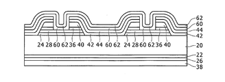
図1は、裏面接合型の光電変換素子10の断面図である。裏面接合型の光電変換素子10は、その受光面の反対側の裏面に、光電変換を行うpn接合を形成し、電極も裏面にのみ設けるものである。このように、受光面に電極を一切配置しないので、受光面積が広く取れ、面積当たりの光電変換効率が向上する。図1では、紙面の下側が受光面側で、上側が裏面である。なお、以下では、特に断らない限り、裏面接合型の光電変換素子10のことを、単に光電変換素子10と呼ぶことにする。
光電変換素子10には、n型のシリコン単結晶基板である半導体基板20の裏面に、n型領域100とp型領域102が設けられる。n型領域100は、半導体基板20に接続し、これと同じ導電型であるn型非晶質半導体層28を含んで構成される。図1では、半導体基板20とn型非晶質半導体層28との間に、i型非晶質半導体層24が設けられるが、i型非晶質半導体層24は必ずしも必須の構成要素ではない。p型領域102は、p型非晶質半導体層44を含んで構成され、半導体基板20とpn接合を形成する。図1では、半導体基板20とp型非晶質半導体層44との間に、i型非晶質半導体層42が設けられるが、i型非晶質半導体層42は必ずしも必須の構成要素ではない。
n型領域用の電極70は、n型非晶質半導体層28に接続されるめっき電極である。電極70は、SnとCuの積層構造である。n型領域用の電極70とn型非晶質半導体層28との間に設けられる下地電極60,62は、電極70をめっきする際に用いられるシード層である。下地電極60,62は、透明電極層60とCu層62の積層構造である。
p型領域用の電極72は、p型非晶質半導体層44に接続されるめっき電極である。電極72は、電極70と同様に、SnとCuの積層構造であり、下地電極60,62を用いてめっきによって形成される。n型領域用の電極70とp型領域用の電極72を比べると、前者の電極高さの方が後者の電極高さよりも高い。これは、前者の下地電極60,62の表面積を後者の下地電極60,62の表面積よりも小さく設定したためである。すなわち、下地電極60,62を共通にしてめっきを行うと、その表面積の差によってめっき電流密度が異なり、小さい表面積の方が速く成長するためである。
図1に示されるように、p型領域用の電極72は、下地電極60,62を介して、p型非晶質半導体層44の上に直接的に設けられる。これに対し、n型領域用の電極70は、酸化シリコン層36と窒化シリコン層40の積層構造の絶縁層に開口部を設け、その開口部を通して、下地電極60,62を介して、n型非晶質半導体層28と接続される。以下で説明するように、この光電変換素子10においては、絶縁層が酸化シリコン層36と窒化シリコン層40の積層構造であることが特徴である。ここで、窒化シリコン層40の厚さは、10nmから500nm程度であるが、酸化シリコン層36の厚さは自然酸化膜の厚さよりも厚く、数nmから200nm程度でよい。
半導体基板20の受光面である表面に設けられるi型非晶質半導体層22とn型非晶質半導体層26は、光電変換が行われる半導体基板20のパッシベーション層としての機能を有する層である。反射防止層38は、受光面における反射を抑制する機能を有する絶縁膜層である。
図2は、光電変換素子10の製造手順を示すフローチャートである。この手順を図3から図16の図を用いて説明する。
最初に、n型のシリコン単結晶基板である半導体基板20が準備される。面方位としては(100)が好ましい。受光面となる表面には、光入射効率を高めるため、テキスチャ構造とすることが好ましい。例えば、シリコンのエッチングの面異方性を利用して、(111)面で囲まれるピラミッド状の凹凸を表面に設けることができる。半導体基板20は、次の工程のために、全体が適当な洗浄液で清浄にされる。
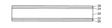
清浄な表面とされた半導体基板20について、次に、i型非晶質半導体層と、n型非晶質半導体層が順次デポジションされる(S10)。デポジションは、堆積とも呼ばれ、薄膜を形成する工程のことである。この工程は、プラズマCVD装置を用いて行うことができる。i型非晶質半導体層とn型非晶質半導体層は、半導体基板20の表面と裏面に共に形成される。図3には、表面にi型非晶質半導体層22とn型非晶質半導体層26が形成され、裏面にi型非晶質半導体層24とn型非晶質半導体層28が形成される様子が示されている。
次に、裏面に酸化シリコン層のデポジションが行われる(S11)。酸化シリコンの代表はSiO2である。この工程は、プラズマCVD装置を用いて行なわれる。酸化シリコン層の厚さは、自然酸化膜が1nm以下であるので、これより厚い数nmから200nm程度が好ましい。酸化シリコン層を設ける役割の1つは、n型非晶質半導体層24の表面を保護し、これによって光電変換効率を向上させることである。もう1つの役割は、HF(弗酸)に溶けやすいので、後述する絶縁膜開口処理のときに、SiNXの残渣をリフトオフにより除去して、清浄なn型非晶質半導体層24の表面とすることである。この役割を利用するために、SiO2を設けているのが、光電変換素子10の特徴である。図4には、裏面において、n型非晶質半導体層28の上に酸化シリコン層36が形成される様子が示される。
次に、窒化シリコン層のデポジションが行われる(S12)。この工程もプラズマCVD装置を用いて行なわれる。窒化シリコンの代表はSi3N4であるが、プラズマCVD装置の製造条件によっては必ずしもSi3N4の組成とならない。一般的にはSiNXの組成となる。窒化シリコン層40の厚さは、10nmから500nm程度である。
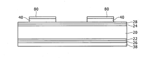
図5では、裏面において、酸化シリコン層36の上に窒化シリコン層40が形成される様子が示される。受光面となる表面には、反射防止層38が形成される。反射防止層38としては、窒化シリコン膜を用いることができるので、裏面の窒化シリコン層40と同じ膜を受光面側にも同時に形成してもよい。しかし、裏面の窒化シリコン層40は、以後のパターニングのために用いられるものでエッチング特性が重要であるのに対し、反射防止層38は光学的特性が重要である。そこで、裏面の窒化シリコン層40と反射防止層38とは、膜特性が異なる絶縁膜とすることがよい。以下では、裏面の窒化シリコン層40と受光面側の反射防止層38とは区別して説明を進める。
なお、裏面の窒化シリコン層40としては、例えば、膜組成を変えることによって、エッチング特性が耐アルカリ性のものと、耐酸性のものと区別して形成することができる。工程の組み方によっては、酸化シリコン層36側を耐酸性の特性の膜とし、その上に耐アルカリ性の膜とすることができる。例えば、レジスト膜をアルカリで除去するものとするときは、レジスト膜に接する側の窒化シリコン層を耐アルカリ性のものとすることがよい。
次に、p型領域102に相当する部分を開口するため、窒化シリコン層40を部分的に除去する(S14)。この処理にはフォトリソグラフィ技術が用いられる。すなわち、窒化シリコン層40の全面に感光性レジスト膜を塗布し、窒化シリコン層40を除去したい部分のレジスト膜を露光して、現像によりその部分のレジスト膜を取り除く。この処理はレジスト膜のパターニングである。そして、レジスト膜をエッチングマスクとして、適当なエッチング液を用いてレジスト膜のない部分の窒化シリコン層40を除去する。エッチング液としてはHFと硝酸の混合液である弗硝酸を用いることができる。エッチングの後は水洗が行われる。
図6には、パターニングされたレジスト膜80と、このレジスト膜80をエッチングマスクとして、残された窒化シリコン層40が示されている。その後、レジスト膜80は除去される。レジスト膜80はアルカリに溶けるので、苛性ソーダ(NaOH)を用いて、窒化シリコン層40をそのままとしてレジスト膜80のみを除去することができる。
次に、p型領域102に相当する部分の半導体基板20を露出させるため、窒化シリコン層40をエッチングマスクとして、その下のn型非晶質半導体層28とi型非晶質半導体層24が除去される(S16)。ここでは、非晶質半導体層がアルカリに溶けることを利用し、苛性ソーダ(NaOH)が用いられる。具体的には、有機洗浄、苛性ソーダ、塩酸(HCl)と過酸化水素(H2O2)の混合液であるSC2、弗酸、水洗の順で処理が行われる。弗酸が用いられるのは、SC2によって酸化膜が形成されるので、それを除去するためである。
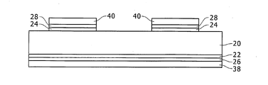
図7には、窒化シリコン層40の形状に、酸化シリコン層36とn型非晶質半導体層28とi型非晶質半導体層24が残され、それ以外の部分に半導体基板20が露出された様子が示される。このようにして、p型領域102の部分の開口が行われる。
次に、i型非晶質半導体層42とp型非晶質半導体層44が全面にデポジションされる(S18)。この工程は、プラズマCVD装置を用いて行なわれる。図8には、開口されたp型領域102の部分において、n型のシリコン単結晶基板である半導体基板20に接触して、i型非晶質半導体層42とp型非晶質半導体層44が配置される様子が示される。なお、窒化シリコン層40の上にも、i型非晶質半導体層42とp型非晶質半導体層44が堆積する。
そして、次に、n型非晶質半導体層28に電極をコンタクトさせるための開口処理が行われる。コンタクトとは、電気的に導通をとることである。図8に示されるように、n型非晶質半導体層28の上には、酸化シリコン層36、窒化シリコン層40、i型非晶質半導体層42、p型非晶質半導体層44が存在しているので、これらを順番に除去する処理が行われる。
最初に、p型非晶質半導体層44とi型非晶質半導体層42の除去が行われる(S20)。この処理にはフォトリソグラフィ技術が用いられる。すなわち、レジスト膜を塗布し、塗布されたレジスト膜について、nコンタクトの部分を露光と現像で除去するパターニングが行われる。レジスト膜には、耐酸性と耐アルカリ性を有する溶剤溶解型が用いられる。これによって、苛性ソーダ(NaOH)を用いて、p型非晶質半導体層44とi型非晶質半導体層42を除去することができる。その後洗浄が行われる。図9には、レジスト膜82の開口部83の部分のp型非晶質半導体層44とi型非晶質半導体層42が除去された様子が示される。
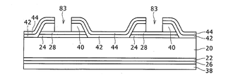
次に、レジスト膜82を残したままで、窒化シリコン層40の除去(S22)と酸化シリコン層36の除去(S23)が行われる。ここでは、弗酸が用いられる。弗酸は、窒化シリコン層40も酸化シリコン層36もエッチングできるが、窒化シリコン層40に対するエッチングレートよりも酸化シリコン層36に対するエッチングレートがかなり速い。また、酸化シリコン層36に対するエッチングレートよりもp型非晶質半導体層28に対するエッチングレートが遅い。すなわち、弗酸を用いると、まず窒化シリコン層40がエッチングされ、酸化シリコン層36に達すると、急速に酸化シリコン層36がエッチングされるが、p型非晶質半導体層28に達するとエッチングが止まる。なお、これらの工程の際に、受光面側の反射防止層38がエッチングされないように、保護膜を設けることが好ましい。
プラズマCVDで形成した窒化シリコンは、弗酸によって除去できるとされるが、実際には、微小な残渣が残り、それを完全に除去するにはかなりの時間を要することがある。その原因としては、例えば、プラズマCVD装置で形成した窒化シリコンがSi3N4の化学量論的な組成ではなく、Si3.5N4のように、Si組成が過剰に多い可能性があることが考えられる。このように、窒化シリコン層40の除去の際に残渣があると、電極とn型非晶質半導体層28との電気的接触が妨げられ、光電変換素子10の光電変換効率が低下することになる。
上記のように、窒化シリコン層40とn型非晶質半導体層28との間に、酸化シリコン層36を配置すると、弗酸を用いて酸化シリコン層36を容易に除去できる。その際に、酸化シリコン層36の上に窒化シリコン層40の残渣があっても、いわゆるリフトオフ現象によって、酸化シリコン層36の上の窒化シリコンが除去される。上記では、窒化シリコン層40をリフトオフによって除去するために酸化シリコン層36と弗酸を用いたが、それ以外でも、絶縁層の残渣をリフトオフで除去しえる中間膜と、その中間膜の除去剤とを組み合わせて用いることができる。
図10は、レジスト膜82を残したままで、窒化シリコン層40と酸化シリコン層36が除去されて、n型非晶質半導体層28のコンタクトのための開口部83が形成された様子が示される。
図11は、リフトオフ現象で、酸化シリコン層36の上の窒化シリコンの残渣41が除去される様子を模式的に示す図である。ここに示されるように、HFとして示した弗酸は、窒化シリコンの残渣41の隙間から酸化シリコン層36に到達し、酸化シリコン層36を溶かすことができる。酸化シリコン層36が溶解すると、窒化シリコンの残渣41は酸化シリコン層36から浮かされて分離される。これによって、酸化シリコン層36の除去と共に、窒化シリコンの残渣41も除去される。
このように、S20、S22,S23の工程において、レジスト膜82を用いて、p型非晶質半導体層44、i型非晶質半導体層42、窒化シリコン層40、酸化シリコン層36が順次除去されて開口部83が形成される。その後、適当な有機溶剤を用いてレジスト膜82が除去される。図11は、レジスト膜82が除去された状態を示す図である。
次に、下地電極形成が行われる(S40)。下地電極は、めっき電極を形成するための導電性のシード層である。具体的には、TCO(Transparent Conductive Oxide)層と呼ばれる透明電極層を全面に形成し、その上にCu層を全面に形成する。透光性導電層としては、インジウム錫酸化物等を用いることができる。
透明電極層であるTCO層の厚さは100nm程度、Cu層の厚さは100nmから1μm程度である。この工程は、スパッタ装置を用いて処理される。図13には、下地電極60,62として、透明電極層60とCu層62の積層構造が全面に形成される様子が示される。
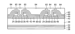
つぎに、電極分離用のレジスト膜が形成される(S42)。これは、n型領域用の電極70とp型領域用の電極72を電気的に分離してめっきするためである。ここでは、レジスト膜を塗布して、露光、現像によってパターニングを行い、n型領域部分とp型領域部分の境界に分離溝を形成する。図14には、分離溝85が形成されたレジスト膜84が示されている。
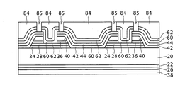
そして、電極用のレジスト膜を用いて、下地電極のエッチングが行われる(S44)。エッチングには、塩化第二鉄と塩酸(HCl)が用いられる。図15には、このエッチングによって、分離溝85のところの下地電極60,62が除去された様子が示される。
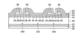
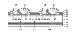
その後、レジスト膜が除去される(S46)。レジスト膜除去には、苛性ソーダ(NaOH)が用いられる。図16にはレジスト膜が除去され、下地電極60,62が分離部86によって、n型領域100用と、p型領域102用とに分離された様子が示される。
次にめっき電極の形成が行われる(S48)。具体的には、硫酸(H2SO4)による洗浄、めっき浴を用いたCuの電解めっきとその後の洗浄、めっき浴を用いたSnの電解めっきとその後の洗浄が順次行われる。Cuめっき層の厚さは10μmから20μm程度、Snめっき層の厚さは1μmから5μmである。このようにして、図1で説明した構造の光電変換素子10が完成する。
次に、酸化シリコン層を用いない光電変換素子の構造と製造方法を比較例として説明する。図17は、図1に対応する図で、絶縁層として、窒化シリコン層40のみを用い、酸化シリコン層を用いない光電変換素子12の断面図である。絶縁層が窒化シリコン層40のみであることを除けば図1と同様の構成であるので、詳細な説明を省略する。
図18は、比較例の光電変換素子12の製造手順を示すフローチャートである。図2と比較すると、酸化シリコン層デポジションのS11の工程と、nコンタクトのための酸化シリコン層の除去のS23の工程が省略されていることが分かる。
図19から図29は、図18の手順における様子を示す図である。図19は、図3に対応する図であるが、ここでは、表面にi型非晶質半導体層22とn型非晶質半導体層26が形成され、裏面にi型非晶質半導体層24とn型非晶質半導体層28が形成される様子が示されている。この構造は、図3と全く同じである。
図20以下は、酸化シリコン層の形成が行われないことから、図3から図16で説明した構造と異なっている。図20は窒化シリコン層40の形成を示す図で、図5に相当するが、n型非晶質半導体層28と窒化シリコン層40との間に酸化シリコン層36が形成されていない。
以下、図21と図6、図22と図7、図23と図8、図24と図9において、いずれも酸化シリコン層36がないことが相違する。そして、図10で説明した酸化シリコン層36の除去工程がなく、図11で説明したリフトオフによる窒化シリコンの残渣41の除去も行われない。
その後、図25と図12、図26と図13、図27と図14、図28と図15、図29と図16と、処理内容は同じであるが、いずれも、n型領域100における絶縁層に酸化シリコン層36がないことが相違する。
このように、窒化シリコン層40と非晶質半導体層との間に、酸化シリコン層36を配置することで、窒化シリコン層40の開口処理の際に、仮に残渣41があっても、これを良好に除去することができる。
本発明に係る裏面接合型の光電変換素子及び裏面接合型の光電変換素子の製造方法は、太陽光発電システム等に利用できる。
10,12 光電変換素子、20 半導体基板、22,24 n型非晶質半導体層、26,28 i型非晶質半導体層、36 酸化シリコン層、38 反射防止層、40 窒化シリコン層、41 残渣、42,44 p型非晶質半導体層、60,62 下地電極(60 透明電極層、62 Cu層)、70,72 電極、80,82,84 レジスト膜、83 開口部、85 分離溝、86 分離部、100 n型領域、102 p型領域。
Claims (4)
- 受光面と、前記受光面の反対側の裏面とを有する第1導電型の半導体基板と、
前記裏面に配置され、前記半導体基板に接続し前記第1導電型を有する非晶質半導体層を含んで構成される第1導電型領域と、
前記裏面に配置され、第2導電型を有する非晶質半導体層を含んで構成され、前記半導体基板とpn接合を形成する第2導電型領域と、
前記第1導電型領域または前記第2導電型領域のいずれか一方の領域の非晶質半導体層の上に形成される絶縁層と、
前記絶縁層に設けられた開口部を通して、その下部に設けられる前記非晶質半導体層に接続し、外部に引き出される電極層と、
を備え、
前記絶縁層は、
その下部に設けられる前記非晶質半導体層に接触して設けられる第1絶縁層と、
第1絶縁層の上に形成される第2絶縁層であって、前記第1絶縁層の開口部を形成する際に、リフトオフによって除去される膜質を有する第2絶縁層と、
を含むことを特徴とする裏面接合型の光電変換素子。 - 請求項1に記載の裏面接合型の光電変換素子において、
前記第1絶縁層が酸化シリコン層であり、
前記第2絶縁層が窒化シリコン層であることを特徴とする裏面接合型の光電変換素子。 - 第1導電型のシリコン基板の受光面とは反対側の裏面にpn接合が形成される裏面接合型の光電変換素子の製造方法であって、
前記第1導電型を有する非晶質半導体層を含んで構成され、前記半導体基板に接続する第1導電型領域を前記裏面に形成する工程と、
第2導電型を有する非晶質半導体層を含んで構成され、前記半導体基板とpn接合を形成する第2導電型領域を前記裏面に形成する工程と、
前記第1導電型領域または前記第2導電型領域のいずれか一方の領域の非晶質半導体層の上に絶縁層を形成する工程と、
前記絶縁層を開口する工程と、
前記絶縁層に設けられた開口部を通して、その下部に設けられる前記非晶質半導体層に接続し、外部に引き出される電極層を形成する工程と、
を含み、
前記絶縁層を形成する工程は、
前記絶縁層の下部に設けられる前記非晶質半導体層に接触して第1絶縁層を形成する工程と、
前記第1絶縁層の上に第2絶縁層を形成する工程と、
を含み、
前記絶縁層を開口する工程は、
前記第2絶縁層を開口する工程と、
前記第2絶縁層に対するエッチングレートよりも前記第1絶縁層に対するエッチングレートが速く、前記第1絶縁層に対するエッチングレートよりも前記絶縁層の下部に設けられる前記非晶質半導体層に対するエッチングレートが遅いエッチングレートを有するエッチング剤で前記第1絶縁層を開口する工程と、
を含むことを特徴とする裏面接合型の光電変換素子の製造方法。 - 請求項3に記載の裏面接合型の光電変換素子の製造方法において、
前記第1絶縁層を形成する工程は、前記第1絶縁層として酸化シリコン層を形成し、
前記第2絶縁層を形成する工程は、前記第2絶縁層として窒化シリコン層を形成し、
前記絶縁層を開口する工程は、
前記第1絶縁層を開口する前記エッチング剤として、HFを含むエッチング液を用いることを特徴とする裏面接合型の光電変換素子の製造方法。
Applications Claiming Priority (2)
| Application Number | Priority Date | Filing Date | Title |
|---|---|---|---|
| JP2011068852 | 2011-03-25 | ||
| JP2011-068852 | 2011-03-25 |
Publications (1)
| Publication Number | Publication Date |
|---|---|
| WO2012132655A1 true WO2012132655A1 (ja) | 2012-10-04 |
Family
ID=46930417
Family Applications (1)
| Application Number | Title | Priority Date | Filing Date |
|---|---|---|---|
| PCT/JP2012/054233 Ceased WO2012132655A1 (ja) | 2011-03-25 | 2012-02-22 | 裏面接合型の光電変換素子及び裏面接合型の光電変換素子の製造方法 |
Country Status (1)
| Country | Link |
|---|---|
| WO (1) | WO2012132655A1 (ja) |
Cited By (10)
| Publication number | Priority date | Publication date | Assignee | Title |
|---|---|---|---|---|
| JP2014075526A (ja) * | 2012-10-05 | 2014-04-24 | Sharp Corp | 光電変換素子および光電変換素子の製造方法 |
| WO2015115360A1 (ja) * | 2014-01-29 | 2015-08-06 | パナソニックIpマネジメント株式会社 | 太陽電池 |
| WO2015114903A1 (ja) * | 2014-01-28 | 2015-08-06 | パナソニックIpマネジメント株式会社 | 太陽電池及びその製造方法 |
| JP2015176952A (ja) * | 2014-03-14 | 2015-10-05 | パナソニックIpマネジメント株式会社 | 太陽電池 |
| JP2016006841A (ja) * | 2014-05-30 | 2016-01-14 | パナソニックIpマネジメント株式会社 | 太陽電池 |
| DE102015218244A1 (de) | 2014-09-25 | 2016-03-31 | Panasonic Intellectual Property Management Co., Ltd. | Solarzelle |
| JP2018093237A (ja) * | 2018-03-08 | 2018-06-14 | パナソニックIpマネジメント株式会社 | 太陽電池 |
| WO2019163784A1 (ja) * | 2018-02-23 | 2019-08-29 | 株式会社カネカ | 太陽電池の製造方法 |
| WO2019163786A1 (ja) * | 2018-02-23 | 2019-08-29 | 株式会社カネカ | 太陽電池の製造方法 |
| JP2021034518A (ja) * | 2019-08-22 | 2021-03-01 | 株式会社カネカ | 太陽電池の製造方法 |
Citations (5)
| Publication number | Priority date | Publication date | Assignee | Title |
|---|---|---|---|---|
| WO2010113750A1 (ja) * | 2009-03-30 | 2010-10-07 | 三洋電機株式会社 | 太陽電池 |
| JP2012028718A (ja) * | 2010-07-28 | 2012-02-09 | Sanyo Electric Co Ltd | 太陽電池の製造方法 |
| JP2012033810A (ja) * | 2010-08-02 | 2012-02-16 | Sanyo Electric Co Ltd | 太陽電池の製造方法 |
| JP2012033666A (ja) * | 2010-07-30 | 2012-02-16 | Sanyo Electric Co Ltd | 太陽電池の製造方法及び太陽電池 |
| JP2012049193A (ja) * | 2010-08-24 | 2012-03-08 | Sanyo Electric Co Ltd | 太陽電池の製造方法 |
-
2012
- 2012-02-22 WO PCT/JP2012/054233 patent/WO2012132655A1/ja not_active Ceased
Patent Citations (5)
| Publication number | Priority date | Publication date | Assignee | Title |
|---|---|---|---|---|
| WO2010113750A1 (ja) * | 2009-03-30 | 2010-10-07 | 三洋電機株式会社 | 太陽電池 |
| JP2012028718A (ja) * | 2010-07-28 | 2012-02-09 | Sanyo Electric Co Ltd | 太陽電池の製造方法 |
| JP2012033666A (ja) * | 2010-07-30 | 2012-02-16 | Sanyo Electric Co Ltd | 太陽電池の製造方法及び太陽電池 |
| JP2012033810A (ja) * | 2010-08-02 | 2012-02-16 | Sanyo Electric Co Ltd | 太陽電池の製造方法 |
| JP2012049193A (ja) * | 2010-08-24 | 2012-03-08 | Sanyo Electric Co Ltd | 太陽電池の製造方法 |
Cited By (21)
| Publication number | Priority date | Publication date | Assignee | Title |
|---|---|---|---|---|
| JP2014075526A (ja) * | 2012-10-05 | 2014-04-24 | Sharp Corp | 光電変換素子および光電変換素子の製造方法 |
| WO2015114903A1 (ja) * | 2014-01-28 | 2015-08-06 | パナソニックIpマネジメント株式会社 | 太陽電池及びその製造方法 |
| JPWO2015114903A1 (ja) * | 2014-01-28 | 2017-03-23 | パナソニックIpマネジメント株式会社 | 太陽電池及びその製造方法 |
| US10014420B2 (en) | 2014-01-29 | 2018-07-03 | Panasonic Intellectual Property Management Co., Ltd. | Solar cell |
| WO2015115360A1 (ja) * | 2014-01-29 | 2015-08-06 | パナソニックIpマネジメント株式会社 | 太陽電池 |
| JPWO2015115360A1 (ja) * | 2014-01-29 | 2017-03-23 | パナソニックIpマネジメント株式会社 | 太陽電池 |
| JP2015176952A (ja) * | 2014-03-14 | 2015-10-05 | パナソニックIpマネジメント株式会社 | 太陽電池 |
| JP2016006841A (ja) * | 2014-05-30 | 2016-01-14 | パナソニックIpマネジメント株式会社 | 太陽電池 |
| US10026853B2 (en) | 2014-05-30 | 2018-07-17 | Panasonic Intellectual Property Management Co., Ltd. | Solar cell |
| DE102015218244A1 (de) | 2014-09-25 | 2016-03-31 | Panasonic Intellectual Property Management Co., Ltd. | Solarzelle |
| WO2019163784A1 (ja) * | 2018-02-23 | 2019-08-29 | 株式会社カネカ | 太陽電池の製造方法 |
| WO2019163786A1 (ja) * | 2018-02-23 | 2019-08-29 | 株式会社カネカ | 太陽電池の製造方法 |
| CN111742416A (zh) * | 2018-02-23 | 2020-10-02 | 株式会社钟化 | 太阳能电池的制造方法 |
| JPWO2019163784A1 (ja) * | 2018-02-23 | 2021-02-04 | 株式会社カネカ | 太陽電池の製造方法 |
| JPWO2019163786A1 (ja) * | 2018-02-23 | 2021-02-04 | 株式会社カネカ | 太陽電池の製造方法 |
| JP7183245B2 (ja) | 2018-02-23 | 2022-12-05 | 株式会社カネカ | 太陽電池の製造方法 |
| JP7237920B2 (ja) | 2018-02-23 | 2023-03-13 | 株式会社カネカ | 太陽電池の製造方法 |
| CN111742416B (zh) * | 2018-02-23 | 2024-03-19 | 株式会社钟化 | 太阳能电池的制造方法 |
| JP2018093237A (ja) * | 2018-03-08 | 2018-06-14 | パナソニックIpマネジメント株式会社 | 太陽電池 |
| JP2021034518A (ja) * | 2019-08-22 | 2021-03-01 | 株式会社カネカ | 太陽電池の製造方法 |
| JP7353865B2 (ja) | 2019-08-22 | 2023-10-02 | 株式会社カネカ | 太陽電池の製造方法 |
Similar Documents
| Publication | Publication Date | Title |
|---|---|---|
| US20260006940A1 (en) | Back-contact solar cell and preparation method therefor | |
| JP5774204B2 (ja) | 光起電力素子およびその製造方法、太陽電池モジュール | |
| JP5891382B2 (ja) | 光電変換素子の製造方法 | |
| JP6817764B2 (ja) | 太陽電池セル、及び太陽電池セルの製造方法 | |
| CN114038922B (zh) | 一种提升绝缘隔离效果的背接触异质结太阳能电池及其制作方法 | |
| CN107210331B (zh) | 太阳能电池及其制造方法 | |
| US20130133729A1 (en) | Solar cell and manufacturing method thereof | |
| WO2012132854A1 (ja) | 光電変換装置及びその製造方法 | |
| JPWO2010064549A1 (ja) | 薄膜光電変換装置の製造方法 | |
| CN118712243A (zh) | 背接触光伏电池及其制备方法 | |
| CN113809186A (zh) | 一种采用形成电极、开槽绝缘二步法的背接触异质结太阳能电池制造方法 | |
| JP2013131586A (ja) | 裏面電極型太陽電池の製造方法 | |
| CN115763609A (zh) | 一种隧穿型背接触异质结太阳能电池及其制作方法 | |
| TWI587540B (zh) | 太陽能電池透明導電膜上實施電鍍製程的方法 | |
| WO2018168180A1 (ja) | 太陽電池およびその製造方法 | |
| WO2019242550A1 (zh) | 太阳能电池及其制作方法 | |
| JP7146786B2 (ja) | 太陽電池の製造方法、太陽電池および太陽電池モジュール | |
| JP5820989B2 (ja) | 光電変換素子の製造方法 | |
| WO2020149128A1 (ja) | 太陽電池の製造方法 | |
| JP7506593B2 (ja) | 太陽電池の製造方法 | |
| CN113809189A (zh) | 一种实现局部制绒的背接触异质结太阳能电池的制造方法 | |
| US20190109253A1 (en) | Solar cell and method for manufacturing same, and solar cell panel | |
| JP6004946B2 (ja) | 太陽電池及び太陽電池モジュール | |
| WO2012132654A1 (ja) | 裏面接合型の光電変換素子及び裏面接合型の光電変換素子の製造方法 | |
| JP2013168605A (ja) | 太陽電池の製造方法 |
Legal Events
| Date | Code | Title | Description |
|---|---|---|---|
| 121 | Ep: the epo has been informed by wipo that ep was designated in this application |
Ref document number: 12765179 Country of ref document: EP Kind code of ref document: A1 |
|
| NENP | Non-entry into the national phase |
Ref country code: DE |
|
| 122 | Ep: pct application non-entry in european phase |
Ref document number: 12765179 Country of ref document: EP Kind code of ref document: A1 |
|
| NENP | Non-entry into the national phase |
Ref country code: JP |