WO2012132126A1 - 有機エレクトロルミネッセンス素子、有機エレクトロルミネッセンス素子の製造方法および電子注入輸送層用塗工液 - Google Patents
有機エレクトロルミネッセンス素子、有機エレクトロルミネッセンス素子の製造方法および電子注入輸送層用塗工液 Download PDFInfo
- Publication number
- WO2012132126A1 WO2012132126A1 PCT/JP2011/078793 JP2011078793W WO2012132126A1 WO 2012132126 A1 WO2012132126 A1 WO 2012132126A1 JP 2011078793 W JP2011078793 W JP 2011078793W WO 2012132126 A1 WO2012132126 A1 WO 2012132126A1
- Authority
- WO
- WIPO (PCT)
- Prior art keywords
- organic
- layer
- metal
- transporting layer
- electron
- Prior art date
- Legal status (The legal status is an assumption and is not a legal conclusion. Google has not performed a legal analysis and makes no representation as to the accuracy of the status listed.)
- Ceased
Links
Images
Classifications
-
- H—ELECTRICITY
- H10—SEMICONDUCTOR DEVICES; ELECTRIC SOLID-STATE DEVICES NOT OTHERWISE PROVIDED FOR
- H10K—ORGANIC ELECTRIC SOLID-STATE DEVICES
- H10K85/00—Organic materials used in the body or electrodes of devices covered by this subclass
- H10K85/30—Coordination compounds
- H10K85/321—Metal complexes comprising a group IIIA element, e.g. Tris (8-hydroxyquinoline) gallium [Gaq3]
- H10K85/322—Metal complexes comprising a group IIIA element, e.g. Tris (8-hydroxyquinoline) gallium [Gaq3] comprising boron
-
- H—ELECTRICITY
- H10—SEMICONDUCTOR DEVICES; ELECTRIC SOLID-STATE DEVICES NOT OTHERWISE PROVIDED FOR
- H10K—ORGANIC ELECTRIC SOLID-STATE DEVICES
- H10K50/00—Organic light-emitting devices
- H10K50/10—OLEDs or polymer light-emitting diodes [PLED]
- H10K50/14—Carrier transporting layers
- H10K50/16—Electron transporting layers
- H10K50/165—Electron transporting layers comprising dopants
-
- H—ELECTRICITY
- H10—SEMICONDUCTOR DEVICES; ELECTRIC SOLID-STATE DEVICES NOT OTHERWISE PROVIDED FOR
- H10K—ORGANIC ELECTRIC SOLID-STATE DEVICES
- H10K50/00—Organic light-emitting devices
- H10K50/10—OLEDs or polymer light-emitting diodes [PLED]
- H10K50/14—Carrier transporting layers
- H10K50/16—Electron transporting layers
- H10K50/166—Electron transporting layers comprising a multilayered structure
-
- H—ELECTRICITY
- H10—SEMICONDUCTOR DEVICES; ELECTRIC SOLID-STATE DEVICES NOT OTHERWISE PROVIDED FOR
- H10K—ORGANIC ELECTRIC SOLID-STATE DEVICES
- H10K50/00—Organic light-emitting devices
- H10K50/10—OLEDs or polymer light-emitting diodes [PLED]
- H10K50/17—Carrier injection layers
- H10K50/171—Electron injection layers
-
- H—ELECTRICITY
- H10—SEMICONDUCTOR DEVICES; ELECTRIC SOLID-STATE DEVICES NOT OTHERWISE PROVIDED FOR
- H10K—ORGANIC ELECTRIC SOLID-STATE DEVICES
- H10K71/00—Manufacture or treatment specially adapted for the organic devices covered by this subclass
- H10K71/10—Deposition of organic active material
- H10K71/12—Deposition of organic active material using liquid deposition, e.g. spin coating
-
- H—ELECTRICITY
- H10—SEMICONDUCTOR DEVICES; ELECTRIC SOLID-STATE DEVICES NOT OTHERWISE PROVIDED FOR
- H10K—ORGANIC ELECTRIC SOLID-STATE DEVICES
- H10K85/00—Organic materials used in the body or electrodes of devices covered by this subclass
- H10K85/10—Organic polymers or oligomers
-
- H—ELECTRICITY
- H10—SEMICONDUCTOR DEVICES; ELECTRIC SOLID-STATE DEVICES NOT OTHERWISE PROVIDED FOR
- H10K—ORGANIC ELECTRIC SOLID-STATE DEVICES
- H10K85/00—Organic materials used in the body or electrodes of devices covered by this subclass
- H10K85/60—Organic compounds having low molecular weight
- H10K85/649—Aromatic compounds comprising a hetero atom
- H10K85/657—Polycyclic condensed heteroaromatic hydrocarbons
- H10K85/6572—Polycyclic condensed heteroaromatic hydrocarbons comprising only nitrogen in the heteroaromatic polycondensed ring system, e.g. phenanthroline or carbazole
-
- H—ELECTRICITY
- H10—SEMICONDUCTOR DEVICES; ELECTRIC SOLID-STATE DEVICES NOT OTHERWISE PROVIDED FOR
- H10K—ORGANIC ELECTRIC SOLID-STATE DEVICES
- H10K85/00—Organic materials used in the body or electrodes of devices covered by this subclass
- H10K85/60—Organic compounds having low molecular weight
- H10K85/658—Organoboranes
Definitions
- Patent Documents 2 and 3 it is described that an electron injection layer is formed by a coating method using a nonionic organometallic complex, a metal phthalocyanine, or an organometallic complex compound. There is no disclosure about its use. In any of Patent Documents 1 to 5, the relationship between the crystalline / amorphous state of the organic layer and device characteristics has not been studied.
- the electron injecting and transporting layer may further contain an electron transporting organic compound.
- the electron injecting and transporting layer contains an organic boron compound and an organic compound, a sufficient carrier balance can be maintained even if the thickness of the electron injecting and transporting layer is increased, so that a sufficient film thickness can be secured. Thus, it is easy to form a uniform film, and the film strength can be increased.
- the driving voltage can be reduced by using an electron-transporting organic compound.
- an organic compound having a hole blocking property in addition to the electron transporting property is added to the electron injecting and transporting layer, the charge recombination probability is improved, and the light emission efficiency can be improved.
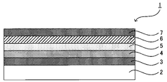
- the present invention also provides an anode, a light emitting layer formed on the anode, an electron injecting and transporting layer containing an organic boron compound formed on the light emitting layer, and a cathode formed on the electron injecting and transporting layer. And an electron injection transport layer forming step of forming an electron injection transport layer by applying a coating solution for an electron injection transport layer containing an organic boron compound and a solvent. Provided is a method for producing a characteristic organic EL element.
- Anode used in the present invention may or may not have optical transparency, and is appropriately selected according to the light extraction surface. When light is extracted from the anode side, the anode becomes a transparent electrode.
- Cathode The cathode used in the present invention may or may not have optical transparency, and is appropriately selected according to the light extraction surface. When light is extracted from the cathode side, the cathode becomes a transparent electrode.
- the cathode preferably has a low resistance, and a metal material that is a conductive material is generally used, but an organic compound or an inorganic compound may be used.
- a conductive material having a small work function is preferably used so that electrons can be easily injected.
- metals such as Li, Ca, Mg, Al and In, Mg alloys such as MgAg, Al alloys such as AlLi, AlCa and AlMg, alkali metals and alkaline earths such as Li, Cs, Ba, Sr and Ca
- An alloy such as a metal alloy can be used.
- metals such as Au, Ag, Pd, Ni, and Cu can also be used.
- the cathode film forming method and patterning method can be the same as the anode film forming method and patterning method.
- the cathode is formed by a wet process, an expensive facility is not required unlike the dry process, which is advantageous in terms of cost.
- the wet process for example, a method of applying a conductive paste in which metal particles such as Au, Ag, Pd, Ni, Cu, etc.
- the melting point of the low melting point metal is preferably 30 ° C. higher than the glass transition temperature of the organic layer such as the light emitting layer, the electron injecting and transporting layer, the hole injecting and transporting layer, specifically 70 ° C. or more and 160 ° C. or less. Is preferred. If the melting point of the low melting point metal is higher than 30 ° C. higher than the glass transition temperature of the organic layer, the organic layer may be seriously damaged. Further, in order to use the organic EL element stably even in a high temperature environment such as in a midsummer car, the lower limit of the melting point of the metal or alloy constituting the electrode is practically 70 ° C.
- Liquid metal is in a liquid state at room temperature (as a guideline, 5 ° C to 45 ° C) and is sufficient at a relatively low temperature of about 50 ° C even at room temperature or even when heated. That shows good fluidity.
- the melting point of the liquid metal is preferably 50 ° C. or less.
- the liquid metal can be formed by a wet process under heating at normal temperature or low temperature, and an electrode having an arbitrary shape can be formed by a wet process regardless of a dry process such as a vapor deposition method.
- the thickness of the hole injecting and transporting layer is not particularly limited as long as the hole injecting function and the hole transporting function are sufficiently exerted.
- the hole injecting and transporting layer has a thickness within the range of 0.5 nm to 1000 nm, particularly 10 nm to It is preferable to be in the range of 500 nm.
- the method for forming the hole injecting and transporting layer can be the same as the method for forming the light emitting layer.
- a partition wall may be formed on the substrate.
- the cathode can be formed in a pattern without using a metal mask or the like.
- a general partition material in an organic EL element can be used.
- a photo-curable resin such as a photosensitive polyimide resin or an acrylic resin, a thermosetting resin, an inorganic material, or the like.
- the partition wall may be subjected in advance to a surface treatment that changes the surface energy (wetting property).
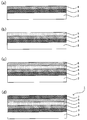
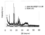
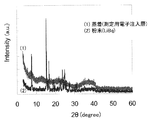
- the organic boron compound is decomposed at the time of film formation as in the vapor deposition method, or an impurity such as a decomposition product of the organic boron compound.
- a crystal film can be obtained without being mixed. The crystal film is presumed to have improved electron transport properties due to the high order of atoms and molecules.
- migration of decomposition products to the light emitting layer occurs during driving of the organic EL element, which may affect the light emission characteristics of the element.
- Example 6 An organic EL device was produced in the same manner as in Example 1 except that the cathode was formed as shown below.
- a metal (alloy) having a composition of Bi—Pb—Sn (50%: 25%: 25%) was melted to form a cathode having a thickness of 30 ⁇ m.
- the metal having the above composition was formed by heating with a hot plate at 103 ° C., which is 10 ° C. higher than the melting point of the metal alloy, and melting the metal on the electron injecting and transporting layer.
Landscapes
- Chemical & Material Sciences (AREA)
- Engineering & Computer Science (AREA)
- Physics & Mathematics (AREA)
- Materials Engineering (AREA)
- Spectroscopy & Molecular Physics (AREA)
- Optics & Photonics (AREA)
- Inorganic Chemistry (AREA)
- Manufacturing & Machinery (AREA)
- Electroluminescent Light Sources (AREA)
Priority Applications (4)
| Application Number | Priority Date | Filing Date | Title |
|---|---|---|---|
| CN201180069665.2A CN103460427B (zh) | 2011-03-31 | 2011-12-13 | 有机电致发光元件、有机电致发光元件的制造方法及电子注入输送层用涂布液 |
| US14/008,243 US8969862B2 (en) | 2011-03-31 | 2011-12-13 | Organic electroluminescent element, method for manufacturing organic electroluminescent element, and coating liquid for electron injection and transport layer |
| KR1020137027726A KR20140015486A (ko) | 2011-03-31 | 2011-12-13 | 유기 일렉트로루미네센스 소자, 유기 일렉트로루미네센스 소자의 제조 방법 및 전자 주입 수송층용 도공액 |
| EP11861994.9A EP2693506B1 (en) | 2011-03-31 | 2011-12-13 | Organic electroluminescent element and method for manufacturing organic electroluminescent element |
Applications Claiming Priority (2)
| Application Number | Priority Date | Filing Date | Title |
|---|---|---|---|
| JP2011078362A JP5655666B2 (ja) | 2011-03-31 | 2011-03-31 | 有機エレクトロルミネッセンス素子、有機エレクトロルミネッセンス素子の製造方法および電子注入輸送層用塗工液 |
| JP2011-078362 | 2011-03-31 |
Publications (1)
| Publication Number | Publication Date |
|---|---|
| WO2012132126A1 true WO2012132126A1 (ja) | 2012-10-04 |
Family
ID=46929923
Family Applications (1)
| Application Number | Title | Priority Date | Filing Date |
|---|---|---|---|
| PCT/JP2011/078793 Ceased WO2012132126A1 (ja) | 2011-03-31 | 2011-12-13 | 有機エレクトロルミネッセンス素子、有機エレクトロルミネッセンス素子の製造方法および電子注入輸送層用塗工液 |
Country Status (5)
| Country | Link |
|---|---|
| US (1) | US8969862B2 (enExample) |
| EP (1) | EP2693506B1 (enExample) |
| JP (1) | JP5655666B2 (enExample) |
| KR (1) | KR20140015486A (enExample) |
| WO (1) | WO2012132126A1 (enExample) |
Cited By (7)
| Publication number | Priority date | Publication date | Assignee | Title |
|---|---|---|---|---|
| WO2020158566A1 (ja) | 2019-01-31 | 2020-08-06 | 大日本印刷株式会社 | 蒸着マスク群、電子デバイスの製造方法及び電子デバイス |
| EP4020585A1 (en) | 2020-12-28 | 2022-06-29 | Dai Nippon Printing Co., Ltd. | Organic device, group of masks, mask, and manufacturing method for organic device |
| EP4020584A1 (en) | 2020-12-28 | 2022-06-29 | Dai Nippon Printing Co., Ltd. | Organic device, group of masks, mask, and manufacturing method for organic device |
| EP4106029A1 (en) | 2021-06-14 | 2022-12-21 | Dai Nippon Printing Co., Ltd. | Mask group, method of manufacturing organic device and organic device |
| EP4109576A2 (en) | 2021-06-21 | 2022-12-28 | Dai Nippon Printing Co., Ltd. | Organic device, group of masks, mask, and manufacturing method for organic device |
| EP4113621A1 (en) | 2021-07-01 | 2023-01-04 | Dai Nippon Printing Co., Ltd. | Organic device and manufacturing method for organic device |
| US11793014B2 (en) | 2020-06-03 | 2023-10-17 | Dai Nippon Printing Co., Ltd. | Electronic device, manufacturing method for electronic device, and deposition mask group |
Families Citing this family (10)
| Publication number | Priority date | Publication date | Assignee | Title |
|---|---|---|---|---|
| CN104067400B (zh) * | 2011-11-30 | 2018-02-27 | 诺瓦尔德股份有限公司 | 有机电子器件 |
| WO2015152148A1 (ja) * | 2014-03-31 | 2015-10-08 | 住友化学株式会社 | 有機エレクトロルミネッセンス素子 |
| JP2015197510A (ja) * | 2014-03-31 | 2015-11-09 | 大日本印刷株式会社 | 有機デバイス |
| CA3010895A1 (en) | 2016-01-21 | 2017-07-27 | SeLux Diagnostics, Inc. | Methods for rapid antimicrobial susceptibility testing |
| US9834808B2 (en) | 2016-01-21 | 2017-12-05 | SeLux Diagnostics, Inc. | Methods for rapid antibiotic susceptibility testing |
| WO2018119439A1 (en) | 2016-12-23 | 2018-06-28 | SeLux Diagnostics, Inc. | Methods for improved rapid antimicrobial susceptibility testing |
| EP3583636B1 (en) | 2017-02-20 | 2023-05-24 | Novaled GmbH | Electronic semiconducting device, method for preparing the electronic semiconducting device and compound |
| KR102892171B1 (ko) * | 2019-02-18 | 2025-11-28 | 삼성디스플레이 주식회사 | 표시 장치 |
| JP2022109223A (ja) * | 2021-01-14 | 2022-07-27 | 住友化学株式会社 | 有機エレクトロルミネッセンス素子の製造方法 |
| CN113948654B (zh) * | 2021-10-26 | 2024-03-01 | 湖南恒显坤光电科技有限公司 | 一种oled器件及其制备方法 |
Citations (14)
| Publication number | Priority date | Publication date | Assignee | Title |
|---|---|---|---|---|
| JP2000252072A (ja) | 1999-03-03 | 2000-09-14 | Honda Motor Co Ltd | 有機エレクトロルミネッセンス素子とその製造方法 |
| JP2001284055A (ja) | 2000-03-29 | 2001-10-12 | Honda Motor Co Ltd | 有機エレクトロルミネッセンス素子とその製造方法 |
| JP2002075651A (ja) * | 2000-09-01 | 2002-03-15 | Sanyo Electric Co Ltd | 有機発光素子 |
| JP2003031367A (ja) * | 2001-07-11 | 2003-01-31 | Konica Corp | 有機エレクトロルミネッセンス素子及び表示装置 |
| JP2003347061A (ja) | 2001-08-20 | 2003-12-05 | Tdk Corp | 有機el素子およびその製造方法 |
| JP2004071395A (ja) * | 2002-08-07 | 2004-03-04 | Seiko Epson Corp | 電気光学装置及びその製造方法、並びに電子機器 |
| JP2005142122A (ja) | 2003-11-10 | 2005-06-02 | Canon Inc | 金属ホウ素酸塩あるいは金属有機ホウ素化物を有する有機発光素子 |
| JP2005285732A (ja) | 2003-12-16 | 2005-10-13 | Dainippon Printing Co Ltd | 有機機能素子およびその製造方法 |
| JP2006048986A (ja) | 2004-08-02 | 2006-02-16 | Sony Corp | 端子構造及び電子機器 |
| JP2006144112A (ja) | 2004-10-20 | 2006-06-08 | Dainippon Printing Co Ltd | Ga系合金及びこれを用いた有機機能素子 |
| JP2009155325A (ja) * | 2007-12-06 | 2009-07-16 | Kyoto Univ | 新規なホウ素化合物、それらの製造方法およびそれらを用いた機能性電子素子 |
| JP2010198935A (ja) * | 2009-02-26 | 2010-09-09 | Dowa Electronics Materials Co Ltd | 有機エレクトロルミネッセンス電極の形成方法及び該形成方法を用いて得られた有機エレクトロルミネッセンス構造体 |
| JP4544937B2 (ja) | 2004-07-30 | 2010-09-15 | 大日本印刷株式会社 | 有機機能素子、有機el素子、有機半導体素子、有機tft素子およびそれらの製造方法 |
| JP2011020970A (ja) * | 2009-07-17 | 2011-02-03 | Showa Denko Kk | ホウ素化合物およびこれを用いた有機エレクトロルミネッセンス素子 |
Family Cites Families (13)
| Publication number | Priority date | Publication date | Assignee | Title |
|---|---|---|---|---|
| US4426366A (en) * | 1980-11-24 | 1984-01-17 | Exxon Research And Engineering Co. | Novel molybdenum oxycarbonitride compositions |
| JP2001131185A (ja) * | 1999-11-05 | 2001-05-15 | Seizo Miyata | ホウ素化合物 |
| JP3990869B2 (ja) * | 2000-03-31 | 2007-10-17 | キヤノン株式会社 | 有機ほう素化合物、該有機ほう素化合物の製造方法、及び該有機ほう素化合物を用いた有機発光素子 |
| JP2003077671A (ja) * | 2001-09-03 | 2003-03-14 | Canon Inc | 有機発光素子 |
| JP2003077670A (ja) * | 2001-09-03 | 2003-03-14 | Canon Inc | 有機発光素子 |
| TW200528536A (en) * | 2003-12-19 | 2005-09-01 | Showa Denko Kk | Boron-containing polymer compound and organic light emitting device using the same |
| JP4603370B2 (ja) * | 2005-01-18 | 2010-12-22 | 創世理工株式会社 | 基板上に作製された半導体光デバイスおよびその作製方法 |
| JP5050333B2 (ja) * | 2005-09-20 | 2012-10-17 | コニカミノルタホールディングス株式会社 | 有機エレクトロルミネッセンス素子 |
| JP5003491B2 (ja) * | 2005-10-28 | 2012-08-15 | コニカミノルタホールディングス株式会社 | 有機エレクトロルミネッセンス素子の製造方法及び製造装置 |
| US7723722B2 (en) * | 2007-03-23 | 2010-05-25 | Semiconductor Energy Laboratory Co., Ltd. | Organic compound, anthracene derivative, and light-emitting element, light-emitting device, and electronic device using anthracene derivative |
| US8076009B2 (en) * | 2007-10-26 | 2011-12-13 | Global Oled Technology, Llc. | OLED device with fluoranthene electron transport materials |
| US8183764B2 (en) * | 2008-03-26 | 2012-05-22 | Toppan Printing Co., Ltd. | Organic electroluminescence element, manufacturing method for an organic electroluminescence element and display unit |
| JP5267246B2 (ja) * | 2008-03-26 | 2013-08-21 | 凸版印刷株式会社 | 有機エレクトロルミネッセンス素子及びその製造方法並びに有機エレクトロルミネッセンス表示装置 |
-
2011
- 2011-03-31 JP JP2011078362A patent/JP5655666B2/ja active Active
- 2011-12-13 EP EP11861994.9A patent/EP2693506B1/en not_active Not-in-force
- 2011-12-13 US US14/008,243 patent/US8969862B2/en not_active Expired - Fee Related
- 2011-12-13 WO PCT/JP2011/078793 patent/WO2012132126A1/ja not_active Ceased
- 2011-12-13 KR KR1020137027726A patent/KR20140015486A/ko not_active Ceased
Patent Citations (15)
| Publication number | Priority date | Publication date | Assignee | Title |
|---|---|---|---|---|
| JP2000252072A (ja) | 1999-03-03 | 2000-09-14 | Honda Motor Co Ltd | 有機エレクトロルミネッセンス素子とその製造方法 |
| JP2001284055A (ja) | 2000-03-29 | 2001-10-12 | Honda Motor Co Ltd | 有機エレクトロルミネッセンス素子とその製造方法 |
| JP3969941B2 (ja) | 2000-09-01 | 2007-09-05 | 三洋電機株式会社 | 有機発光素子 |
| JP2002075651A (ja) * | 2000-09-01 | 2002-03-15 | Sanyo Electric Co Ltd | 有機発光素子 |
| JP2003031367A (ja) * | 2001-07-11 | 2003-01-31 | Konica Corp | 有機エレクトロルミネッセンス素子及び表示装置 |
| JP2003347061A (ja) | 2001-08-20 | 2003-12-05 | Tdk Corp | 有機el素子およびその製造方法 |
| JP2004071395A (ja) * | 2002-08-07 | 2004-03-04 | Seiko Epson Corp | 電気光学装置及びその製造方法、並びに電子機器 |
| JP2005142122A (ja) | 2003-11-10 | 2005-06-02 | Canon Inc | 金属ホウ素酸塩あるいは金属有機ホウ素化物を有する有機発光素子 |
| JP2005285732A (ja) | 2003-12-16 | 2005-10-13 | Dainippon Printing Co Ltd | 有機機能素子およびその製造方法 |
| JP4544937B2 (ja) | 2004-07-30 | 2010-09-15 | 大日本印刷株式会社 | 有機機能素子、有機el素子、有機半導体素子、有機tft素子およびそれらの製造方法 |
| JP2006048986A (ja) | 2004-08-02 | 2006-02-16 | Sony Corp | 端子構造及び電子機器 |
| JP2006144112A (ja) | 2004-10-20 | 2006-06-08 | Dainippon Printing Co Ltd | Ga系合金及びこれを用いた有機機能素子 |
| JP2009155325A (ja) * | 2007-12-06 | 2009-07-16 | Kyoto Univ | 新規なホウ素化合物、それらの製造方法およびそれらを用いた機能性電子素子 |
| JP2010198935A (ja) * | 2009-02-26 | 2010-09-09 | Dowa Electronics Materials Co Ltd | 有機エレクトロルミネッセンス電極の形成方法及び該形成方法を用いて得られた有機エレクトロルミネッセンス構造体 |
| JP2011020970A (ja) * | 2009-07-17 | 2011-02-03 | Showa Denko Kk | ホウ素化合物およびこれを用いた有機エレクトロルミネッセンス素子 |
Non-Patent Citations (2)
| Title |
|---|
| J. APPL. PHYS., vol. 48, 1977, pages 4729 |
| See also references of EP2693506A4 |
Cited By (15)
| Publication number | Priority date | Publication date | Assignee | Title |
|---|---|---|---|---|
| US11566316B2 (en) | 2019-01-31 | 2023-01-31 | Dai Nippon Printing Co., Ltd. | Deposition mask group, manufacturing method of electronic device, and electronic device |
| EP4016658A1 (en) | 2019-01-31 | 2022-06-22 | Dai Nippon Printing Co., Ltd. | Deposition mask group, manufacturing method of electronic device, and electronic device |
| US11939659B2 (en) | 2019-01-31 | 2024-03-26 | Dai Nippon Printing Co., Ltd. | Deposition mask group, manufacturing method of electronic device, and electronic device |
| WO2020158566A1 (ja) | 2019-01-31 | 2020-08-06 | 大日本印刷株式会社 | 蒸着マスク群、電子デバイスの製造方法及び電子デバイス |
| US11649539B2 (en) | 2019-01-31 | 2023-05-16 | Dai Nippon Printing Co., Ltd. | Deposition mask group, manufacturing method of electronic device, and electronic device |
| US11793014B2 (en) | 2020-06-03 | 2023-10-17 | Dai Nippon Printing Co., Ltd. | Electronic device, manufacturing method for electronic device, and deposition mask group |
| EP4020584A1 (en) | 2020-12-28 | 2022-06-29 | Dai Nippon Printing Co., Ltd. | Organic device, group of masks, mask, and manufacturing method for organic device |
| EP4020585A1 (en) | 2020-12-28 | 2022-06-29 | Dai Nippon Printing Co., Ltd. | Organic device, group of masks, mask, and manufacturing method for organic device |
| US12219790B2 (en) | 2020-12-28 | 2025-02-04 | Dai Nippon Printing Co., Ltd. | Organic device, group of masks, mask, and manufacturing method for organic device |
| US12239006B2 (en) | 2020-12-28 | 2025-02-25 | Dai Nippon Printing Co., Ltd. | Organic device having a first display area, and a second display area including a second electrode surrounding each of first and second adjacent transmission areas |
| EP4106029A1 (en) | 2021-06-14 | 2022-12-21 | Dai Nippon Printing Co., Ltd. | Mask group, method of manufacturing organic device and organic device |
| US12410507B2 (en) | 2021-06-14 | 2025-09-09 | Dai Nippon Printing Co., Ltd. | Mask group, method of manufacturing organic device and organic device |
| EP4109576A2 (en) | 2021-06-21 | 2022-12-28 | Dai Nippon Printing Co., Ltd. | Organic device, group of masks, mask, and manufacturing method for organic device |
| EP4113621A1 (en) | 2021-07-01 | 2023-01-04 | Dai Nippon Printing Co., Ltd. | Organic device and manufacturing method for organic device |
| US12453242B2 (en) | 2021-07-01 | 2025-10-21 | Dai Nippon Printing Co., Ltd. | Organic device and manufacturing method for organic device |
Also Published As
| Publication number | Publication date |
|---|---|
| US8969862B2 (en) | 2015-03-03 |
| EP2693506A1 (en) | 2014-02-05 |
| KR20140015486A (ko) | 2014-02-06 |
| CN103460427A (zh) | 2013-12-18 |
| EP2693506B1 (en) | 2019-02-27 |
| EP2693506A4 (en) | 2014-11-19 |
| JP5655666B2 (ja) | 2015-01-21 |
| US20140008638A1 (en) | 2014-01-09 |
| JP2012212813A (ja) | 2012-11-01 |
Similar Documents
| Publication | Publication Date | Title |
|---|---|---|
| JP5655666B2 (ja) | 有機エレクトロルミネッセンス素子、有機エレクトロルミネッセンス素子の製造方法および電子注入輸送層用塗工液 | |
| TWI530484B (zh) | 可溶液加工之摻雜三芳胺之電洞注入材料 | |
| KR101688317B1 (ko) | 저전압 구동 유기발광소자 및 이의 제조 방법 | |
| KR101974233B1 (ko) | 유기 전계 발광 소자 | |
| JP5371404B2 (ja) | 電子輸送性材料および発光素子 | |
| EP3667755A1 (en) | Organic light emitting device, a method for manufacturing the same and a composition for use therein | |
| KR101650705B1 (ko) | 산화 그래핀 기반 유기 발광 다이오드 및 이의 제조 방법 | |
| WO2017216557A1 (en) | Methods for the production of organic electronic devices | |
| TWI775802B (zh) | 發光層形成用組成物以及含有該發光層形成用組成物的有機電場發光元件 | |
| JP2018016641A (ja) | イリジウム錯体化合物、有機電界発光素子、表示装置ならびに照明装置 | |
| KR20160047297A (ko) | 유기 전계 발광 소자 | |
| JP2007201474A (ja) | 電子輸送層用組成物、これを用いた電子輸送層、および電子輸送層を備える有機電界発光素子 | |
| JP2010212676A (ja) | 有機発光デバイス | |
| KR20170008683A (ko) | 유기 el 소자 | |
| CN102696127A (zh) | 有机el 元件及有机发光器件 | |
| KR102919283B1 (ko) | 발광 소자 | |
| CN101981725B (zh) | 有机电致发光元件及其制造方法 | |
| WO2012090560A1 (ja) | 有機エレクトロルミネッセンス素子およびその製造方法 | |
| KR101883770B1 (ko) | 유기 전계 발광 소자용 화합물, 이를 이용한 유기 전계 발광 소자 및 그 제조 방법 | |
| CN106716669A (zh) | 有机电致发光元件用组合物、有机电致发光元件、显示装置以及照明装置 | |
| JP2007100083A (ja) | 有機電界発光素子用組成物及び有機電界発光素子 | |
| JP6511657B2 (ja) | 有機金属錯体、有機エレクトロルミネッセンス素子およびその製造方法、表示装置、照明装置、有機薄膜太陽電池 | |
| JP7232616B2 (ja) | 有機素子 | |
| CN103460427B (zh) | 有机电致发光元件、有机电致发光元件的制造方法及电子注入输送层用涂布液 | |
| JP6724294B2 (ja) | 有機電界発光素子用組成物、有機電界発光素子、表示装置及び照明装置 |
Legal Events
| Date | Code | Title | Description |
|---|---|---|---|
| 121 | Ep: the epo has been informed by wipo that ep was designated in this application |
Ref document number: 11861994 Country of ref document: EP Kind code of ref document: A1 |
|
| WWE | Wipo information: entry into national phase |
Ref document number: 14008243 Country of ref document: US |
|
| NENP | Non-entry into the national phase |
Ref country code: DE |
|
| ENP | Entry into the national phase |
Ref document number: 20137027726 Country of ref document: KR Kind code of ref document: A |
|
| WWE | Wipo information: entry into national phase |
Ref document number: 2011861994 Country of ref document: EP |