WO2012120731A1 - 半導体装置の製造方法 - Google Patents
半導体装置の製造方法 Download PDFInfo
- Publication number
- WO2012120731A1 WO2012120731A1 PCT/JP2011/076267 JP2011076267W WO2012120731A1 WO 2012120731 A1 WO2012120731 A1 WO 2012120731A1 JP 2011076267 W JP2011076267 W JP 2011076267W WO 2012120731 A1 WO2012120731 A1 WO 2012120731A1
- Authority
- WO
- WIPO (PCT)
- Prior art keywords
- substrate
- semiconductor device
- protective film
- manufacturing
- region
- Prior art date
Links
Images


Classifications
-
- H—ELECTRICITY
- H01—ELECTRIC ELEMENTS
- H01L—SEMICONDUCTOR DEVICES NOT COVERED BY CLASS H10
- H01L21/00—Processes or apparatus adapted for the manufacture or treatment of semiconductor or solid state devices or of parts thereof
- H01L21/02—Manufacture or treatment of semiconductor devices or of parts thereof
- H01L21/04—Manufacture or treatment of semiconductor devices or of parts thereof the devices having potential barriers, e.g. a PN junction, depletion layer or carrier concentration layer
- H01L21/18—Manufacture or treatment of semiconductor devices or of parts thereof the devices having potential barriers, e.g. a PN junction, depletion layer or carrier concentration layer the devices having semiconductor bodies comprising elements of Group IV of the Periodic Table or AIIIBV compounds with or without impurities, e.g. doping materials
- H01L21/30—Treatment of semiconductor bodies using processes or apparatus not provided for in groups H01L21/20 - H01L21/26
- H01L21/324—Thermal treatment for modifying the properties of semiconductor bodies, e.g. annealing, sintering
- H01L21/3247—Thermal treatment for modifying the properties of semiconductor bodies, e.g. annealing, sintering for altering the shape, e.g. smoothing the surface
-
- H—ELECTRICITY
- H01—ELECTRIC ELEMENTS
- H01L—SEMICONDUCTOR DEVICES NOT COVERED BY CLASS H10
- H01L21/00—Processes or apparatus adapted for the manufacture or treatment of semiconductor or solid state devices or of parts thereof
- H01L21/02—Manufacture or treatment of semiconductor devices or of parts thereof
- H01L21/04—Manufacture or treatment of semiconductor devices or of parts thereof the devices having potential barriers, e.g. a PN junction, depletion layer or carrier concentration layer
- H01L21/0445—Manufacture or treatment of semiconductor devices or of parts thereof the devices having potential barriers, e.g. a PN junction, depletion layer or carrier concentration layer the devices having semiconductor bodies comprising crystalline silicon carbide
- H01L21/0455—Making n or p doped regions or layers, e.g. using diffusion
- H01L21/046—Making n or p doped regions or layers, e.g. using diffusion using ion implantation
-
- H—ELECTRICITY
- H01—ELECTRIC ELEMENTS
- H01L—SEMICONDUCTOR DEVICES NOT COVERED BY CLASS H10
- H01L21/00—Processes or apparatus adapted for the manufacture or treatment of semiconductor or solid state devices or of parts thereof
- H01L21/02—Manufacture or treatment of semiconductor devices or of parts thereof
- H01L21/02104—Forming layers
- H01L21/02107—Forming insulating materials on a substrate
- H01L21/02225—Forming insulating materials on a substrate characterised by the process for the formation of the insulating layer
- H01L21/0226—Forming insulating materials on a substrate characterised by the process for the formation of the insulating layer formation by a deposition process
- H01L21/02293—Forming insulating materials on a substrate characterised by the process for the formation of the insulating layer formation by a deposition process formation of epitaxial layers by a deposition process
-
- H—ELECTRICITY
- H01—ELECTRIC ELEMENTS
- H01L—SEMICONDUCTOR DEVICES NOT COVERED BY CLASS H10
- H01L21/00—Processes or apparatus adapted for the manufacture or treatment of semiconductor or solid state devices or of parts thereof
- H01L21/02—Manufacture or treatment of semiconductor devices or of parts thereof
- H01L21/04—Manufacture or treatment of semiconductor devices or of parts thereof the devices having potential barriers, e.g. a PN junction, depletion layer or carrier concentration layer
- H01L21/18—Manufacture or treatment of semiconductor devices or of parts thereof the devices having potential barriers, e.g. a PN junction, depletion layer or carrier concentration layer the devices having semiconductor bodies comprising elements of Group IV of the Periodic Table or AIIIBV compounds with or without impurities, e.g. doping materials
- H01L21/20—Deposition of semiconductor materials on a substrate, e.g. epitaxial growth solid phase epitaxy
-
- H—ELECTRICITY
- H01—ELECTRIC ELEMENTS
- H01L—SEMICONDUCTOR DEVICES NOT COVERED BY CLASS H10
- H01L21/00—Processes or apparatus adapted for the manufacture or treatment of semiconductor or solid state devices or of parts thereof
- H01L21/02—Manufacture or treatment of semiconductor devices or of parts thereof
- H01L21/04—Manufacture or treatment of semiconductor devices or of parts thereof the devices having potential barriers, e.g. a PN junction, depletion layer or carrier concentration layer
- H01L21/18—Manufacture or treatment of semiconductor devices or of parts thereof the devices having potential barriers, e.g. a PN junction, depletion layer or carrier concentration layer the devices having semiconductor bodies comprising elements of Group IV of the Periodic Table or AIIIBV compounds with or without impurities, e.g. doping materials
- H01L21/30—Treatment of semiconductor bodies using processes or apparatus not provided for in groups H01L21/20 - H01L21/26
- H01L21/324—Thermal treatment for modifying the properties of semiconductor bodies, e.g. annealing, sintering
-
- H—ELECTRICITY
- H10—SEMICONDUCTOR DEVICES; ELECTRIC SOLID-STATE DEVICES NOT OTHERWISE PROVIDED FOR
- H10D—INORGANIC ELECTRIC SEMICONDUCTOR DEVICES
- H10D12/00—Bipolar devices controlled by the field effect, e.g. insulated-gate bipolar transistors [IGBT]
- H10D12/01—Manufacture or treatment
- H10D12/031—Manufacture or treatment of IGBTs
-
- H—ELECTRICITY
- H10—SEMICONDUCTOR DEVICES; ELECTRIC SOLID-STATE DEVICES NOT OTHERWISE PROVIDED FOR
- H10D—INORGANIC ELECTRIC SEMICONDUCTOR DEVICES
- H10D30/00—Field-effect transistors [FET]
- H10D30/01—Manufacture or treatment
- H10D30/021—Manufacture or treatment of FETs having insulated gates [IGFET]
- H10D30/028—Manufacture or treatment of FETs having insulated gates [IGFET] of double-diffused metal oxide semiconductor [DMOS] FETs
- H10D30/0291—Manufacture or treatment of FETs having insulated gates [IGFET] of double-diffused metal oxide semiconductor [DMOS] FETs of vertical DMOS [VDMOS] FETs
-
- H—ELECTRICITY
- H10—SEMICONDUCTOR DEVICES; ELECTRIC SOLID-STATE DEVICES NOT OTHERWISE PROVIDED FOR
- H10D—INORGANIC ELECTRIC SEMICONDUCTOR DEVICES
- H10D30/00—Field-effect transistors [FET]
- H10D30/60—Insulated-gate field-effect transistors [IGFET]
- H10D30/64—Double-diffused metal-oxide semiconductor [DMOS] FETs
- H10D30/66—Vertical DMOS [VDMOS] FETs
-
- H—ELECTRICITY
- H10—SEMICONDUCTOR DEVICES; ELECTRIC SOLID-STATE DEVICES NOT OTHERWISE PROVIDED FOR
- H10D—INORGANIC ELECTRIC SEMICONDUCTOR DEVICES
- H10D62/00—Semiconductor bodies, or regions thereof, of devices having potential barriers
- H10D62/80—Semiconductor bodies, or regions thereof, of devices having potential barriers characterised by the materials
- H10D62/83—Semiconductor bodies, or regions thereof, of devices having potential barriers characterised by the materials being Group IV materials, e.g. B-doped Si or undoped Ge
- H10D62/832—Semiconductor bodies, or regions thereof, of devices having potential barriers characterised by the materials being Group IV materials, e.g. B-doped Si or undoped Ge being Group IV materials comprising two or more elements, e.g. SiGe
- H10D62/8325—Silicon carbide
Definitions
- the present invention relates to a method for manufacturing a semiconductor device, and more specifically, a method for manufacturing a semiconductor device capable of suppressing surface roughness of a substrate in activation annealing for activating impurities introduced into a substrate made of silicon carbide. It is about.
- silicon carbide has been increasingly adopted as a material constituting semiconductor devices in order to enable higher breakdown voltage, lower loss, and use in high-temperature environments.
- Silicon carbide is a wide band gap semiconductor having a larger band gap than silicon that has been widely used as a material for forming semiconductor devices. Therefore, by adopting silicon carbide as a material constituting the semiconductor device, it is possible to achieve a high breakdown voltage and a low on-resistance of the semiconductor device.
- a semiconductor device that employs silicon carbide as a material has an advantage that a decrease in characteristics when used in a high temperature environment is small as compared with a semiconductor device that employs silicon as a material.
- activation annealing for activating the impurity is performed.
- activation annealing of a substrate made of silicon carbide needs to be performed at a high temperature.
- surface roughness of the substrate may occur due to activation annealing. Since the surface roughness may adversely affect the characteristics of the semiconductor device to be manufactured, it is desirable to reduce the surface roughness.
- a method for manufacturing a silicon carbide semiconductor device has been proposed in which the surface of an ion-implanted region is covered with a silicon nitride film before activation annealing of impurities introduced by ion implantation (for example, JP-A-7-86199 (Patent Document 1)).
- the substrate needs to be heated to a high temperature of 1600 ° C. or higher. Therefore, in the method of manufacturing a semiconductor device described in Patent Document 1, there is a risk that a crack may occur in the silicon nitride film due to a difference in linear expansion coefficient between silicon carbide and silicon nitride. And when a crack arises in the silicon nitride film as a protective film, the problem that the surface roughness of a board
- the present invention has been made to address such problems, and an object thereof is to provide a method of manufacturing a semiconductor device capable of suppressing surface roughness in activation annealing of a substrate made of silicon carbide. That is.
- a method of manufacturing a semiconductor device includes a step of preparing a substrate made of silicon carbide, a step of performing ion implantation on the substrate, and forming a protective film made of silicon dioxide on the substrate on which ion implantation has been performed. And a step of heating the substrate on which the protective film is formed to a temperature range of 1600 ° C. or higher in an atmosphere containing a gas containing oxygen atoms.
- a protective film made of silicon dioxide is formed on a substrate made of silicon carbide on which ion implantation has been performed, and then a temperature of 1600 ° C. or higher in an atmosphere containing a gas containing oxygen atoms.
- Activation annealing is performed by heating the zone.
- the crack is caused by the silicon dioxide generated by the combination of the silicon released from the silicon carbide substrate and the oxygen atoms contained in the gas in the atmosphere. Is suppressed.
- surface roughness in activation annealing of a substrate made of silicon carbide can be suppressed.
- the substrate on which the protective film is formed in the step of heating the substrate, may be heated to a temperature range of 1700 ° C. or lower.
- the heating temperature of the substrate By setting the heating temperature of the substrate to 1700 ° C. or less, it becomes possible to more reliably suppress the surface roughness of the substrate by the protective film made of silicon dioxide.
- the substrate on which the protective film is formed is heated in an atmosphere containing oxygen gas.
- oxygen gas Since oxygen gas is inexpensive and easy to handle, it is suitable as a gas (gas containing oxygen atoms) constituting the atmosphere of the process of heating the substrate.
- the protective film may be formed by thermal oxidation in the step of forming the protective film.
- the protective film made of silicon dioxide can be easily formed.
- the step of forming the protective film and the step of heating the substrate may be performed as a single step.
- the substrate is heated in an atmosphere containing a gas containing oxygen atoms. Therefore, the step of forming the protective film and the step of heating the substrate in an atmosphere containing a gas containing oxygen atoms can be performed as a single step. Thereby, the manufacturing process of the semiconductor device can be simplified.
- the method for manufacturing a semiconductor device of the present invention it is possible to provide a method for manufacturing a semiconductor device capable of suppressing surface roughness in activation annealing of a substrate made of silicon carbide. it can.
- MOSFET Metal Oxide Semiconductor Field Effect Transistor
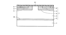
- MOSFET 100 as a semiconductor device is a DiMOSFET, and includes a silicon carbide substrate 1 having a conductivity type of n type (first conductivity type) and a buffer made of silicon carbide and having a conductivity type of n type.
- Layer 2 drift layer 3 made of silicon carbide and having n conductivity type, a pair of p type body regions 4 having conductivity type of p type (second conductivity type), and n + region 5 having conductivity type of n type.
- p + region 6 having a conductivity type of p type.
- Buffer layer 2 is formed on one main surface 1A of silicon carbide substrate 1 and has an n-type conductivity by including an n-type impurity.
- Drift layer 3 is formed on buffer layer 2 and has an n-type conductivity by including an n-type impurity.
- the n-type impurity contained in the drift layer 3 is, for example, N (nitrogen), and is contained at a lower concentration (density) than the n-type impurity contained in the buffer layer 2.
- Buffer layer 2 and drift layer 3 are epitaxial growth layers formed on one main surface 1 ⁇ / b> A of silicon carbide substrate 1.
- the pair of p-type body regions 4 are formed separately from each other so as to include a main surface 3A opposite to the main surface on the silicon carbide substrate 1 side in the epitaxial growth layer, and p-type impurities (conductivity type is p-type). By including an impurity), the conductivity type is p-type.
- the p-type impurity contained in p-type body region 4 is, for example, aluminum (Al), boron (B), or the like.
- the n + region 5 is formed inside each of the pair of p-type body regions 4 so as to include the main surface 3 ⁇ / b > A and be surrounded by the p-type body region 4.
- the n + region 5 contains an n-type impurity, such as P, at a higher concentration (density) than the n-type impurity contained in the drift layer 3.
- P + region 6 includes main surface 3 ⁇ / b > A , is surrounded by p type body region 4, and is formed inside each of the pair of p type body regions 4 so as to be adjacent to n + region 5.
- the p + region 6 contains a p-type impurity such as Al at a higher concentration (density) than the p-type impurity contained in the p-type body region 4.
- the buffer layer 2, the drift layer 3, the p-type body region 4, the n + region 5 and the p + region 6 constitute an active layer 7.
- MOSFET 100 includes a gate oxide film 91 as a gate insulating film, a gate electrode 93, a pair of source contact electrodes 92, an interlayer insulating film 94, a source wiring 95, and a drain electrode 96. And.
- Gate oxide film 91 is formed on main surface 3A of the epitaxial growth layer so as to contact main surface 3A and extend from the upper surface of one n + region 5 to the upper surface of the other n + region 5,
- it is made of silicon dioxide (SiO 2 ).
- Gate electrode 93 is arranged in contact with gate oxide film 91 so as to extend from one n + region 5 to the other n + region 5.
- the gate electrode 93 is made of a conductor such as polysilicon or Al to which impurities are added.
- Source contact electrode 92 extends from each of the pair of n + regions 5 in a direction away from gate oxide film 91 to reach p + region 6 and is in contact with main surface 3A. .
- the source contact electrode 92 is made of a material capable of ohmic contact with the n + region 5 such as Ni x Si y (nickel silicide).
- Interlayer insulating film 94 is formed to surround gate electrode 93 on main surface 3A of drift layer 3 and to extend from one p-type body region 4 to the other p-type body region 4, for example, it is made from silicon dioxide (SiO 2) which is an insulator.
- Source wiring 95 surrounds interlayer insulating film 94 on main surface 3 ⁇ / b> A of drift layer 3 and extends to the upper surface of source contact electrode 92.
- the source wiring 95 is made of a conductor such as Al and is electrically connected to the n + region 5 through the source contact electrode 92.
- Drain electrode 96 is formed in contact with the main surface of silicon carbide substrate 1 opposite to the side on which drift layer 3 is formed. Drain electrode 96 is made of a material capable of making ohmic contact with silicon carbide substrate 1 such as Ni x Si y , and is electrically connected to silicon carbide substrate 1.
- MOSFET 100 in the state where the voltage of gate electrode 93 is lower than the threshold voltage, that is, in the off state, even if a voltage is applied to the drain electrode, p-type body region 4 located immediately below gate oxide film 91 drifts. The pn junction with the layer 3 is reverse-biased and becomes non-conductive.
- a voltage equal to or higher than the threshold voltage is applied to the gate electrode 93, an inversion layer is formed in the channel region in the vicinity of the p-type body region 4 in contact with the gate oxide film 91.
- n + region 5 and drift layer 3 are electrically connected, and a current flows between source line 95 and drain electrode 96.
- MOSFET 100 an inversion layer is formed in the channel region, which is a region in contact with gate oxide film 91 of p-type body region 4, and current flows through the inversion layer. For this reason, when surface roughness occurs on the main surface 3A, the resistance (channel resistance) in the inversion layer increases and the on-resistance increases.
- MOSFET 100 in the present embodiment is manufactured by the method for manufacturing a semiconductor device in the present embodiment described below, so that surface roughness of main surface 3A is reduced and the occurrence of the above problem is suppressed. Yes.
- a method for manufacturing MOSFET 100 in the present embodiment will be described with reference to FIGS.
- a silicon carbide substrate preparation step is performed as a step (S110).
- silicon carbide substrate 1 obtained by slicing an ingot manufactured by a sublimation method is prepared.
- an epitaxial growth step is performed as a step (S120).
- step (S120) referring to FIG. 3, buffer layer 2 and drift layer 3 made of silicon carbide are sequentially formed on one main surface 1A of silicon carbide substrate 1 by epitaxial growth. Thereby, substrate 8 with an epitaxial growth layer as a substrate made of silicon carbide is obtained.
- an ion implantation step is performed as a step (S130).
- step (S130) referring to FIGS. 3 and 4, first, ion implantation for forming p type body region 4 is performed. Specifically, for example, Al (aluminum) ions are implanted into drift layer 3 to form p-type body region 4. Next, ion implantation for forming the n + region 5 is performed. Specifically, for example, P (phosphorus) ions are implanted into p type body region 4 to form n + region 5 in p type body region 4. Further, ion implantation for forming the p + region 6 is performed.
- Al ions are implanted into the p-type body region 4, thereby forming a p + region 6 in the p-type body region 4.
- the ion implantation can be performed by, for example, forming a mask layer made of silicon dioxide (SiO 2 ) on the main surface of the drift layer 3 and having an opening in a desired region where ion implantation is to be performed.
- a protective film forming step is performed as a step (S140).
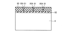
- protective film 80 made of silicon dioxide is formed on main surface 3A of substrate 8 with the epitaxial growth layer on which ion implantation has been performed in step (S130).
- This protective film 80 can be formed by thermal oxidation, for example.
- the thickness of the protective film 80 can be 0.1 micrometer or more and 1 micrometer or less, for example.
- the protective film 80 may be formed by a CVD method such as plasma CVD (Chemical Vapor Deposition).
- an activation annealing step is performed as a step (S150).
- the substrate 8 with the epitaxial growth layer on which the protective film 80 is formed in the step (S140) is heated to a temperature range of 1600 ° C. or higher in an atmosphere containing a gas containing oxygen atoms.
- the impurity introduced into the substrate 8 with the epitaxial growth layer by ion implantation in the step (S130) is activated, and the p-type body region 4, n + region 5 and p + region 6 of desired conductivity type are obtained.
- the substrate 8 with an epitaxial growth layer is heated in an atmosphere containing a gas containing oxygen atoms. Therefore, the silicon separated from the epitaxial growth layer-attached substrate 8 is combined with oxygen in the atmosphere to become silicon dioxide.
- a silicon dioxide film 82 is formed at the boundary between the substrate 8 with the epitaxial growth layer and the protective film 80, and a crack suppressing portion 81 that is made of silicon dioxide and fills (repairs) the crack 80A. Is formed. Thereby, generation
- the gas containing oxygen atoms for example, oxygen gas, ozone gas, nitrogen monoxide gas, nitrogen dioxide gas, carbon monoxide gas and the like can be employed.
- Oxygen gas is particularly suitable as the gas containing oxygen atoms because it is inexpensive and easy to handle.
- the substrate 8 with an epitaxial growth layer may be heated in an oxygen gas atmosphere or an atmosphere containing oxygen gas and argon gas and remaining impurities.
- the heating temperature of the substrate 8 with an epitaxial growth layer is preferably 1700 ° C. or lower.
- the surface roughness can be more reliably suppressed by the protective film 80, the silicon dioxide film 82, and the crack suppressing portion 81 made of silicon dioxide.
- the steps (S140) and (S150) may be performed as a single step.
- the substrate 8 with an epitaxial growth layer is heated to a temperature range of 1100 ° C. or higher and 1600 ° C. or lower for 5 minutes in a reaction chamber containing oxygen gas and argon gas and adjusted to an atmosphere composed of the remaining impurities.
- the heating time is 1600 ° C. or more and 1700 ° C. or less for 1 minute or more and 30 minutes or less in the same reaction chamber without changing the atmosphere.
- Activation annealing is performed by holding.
- the process of manufacturing MOSFET 100 can be simplified by performing steps (S140) and (S150) as a single step.
- a protective film removal step is performed as a step (S160).
- the protective film 80 is removed.
- the removal of the protective film 80 may be performed using, for example, a hydrofluoric acid-based liquid or may be performed by a fluorine-based plasma treatment.
- an oxide film forming step is performed as a step (S170).
- this step (S170) referring to FIG. 8, for example, an oxide film (gate oxide film) 91 is formed by performing a heat treatment of heating to 1300 ° C. and holding for 60 minutes in an oxygen atmosphere.
- an electrode forming step is performed as a step (S180).
- gate electrode 93 made of polysilicon which is a conductor doped with impurities at a high concentration is formed by, for example, CVD, photolithography and etching. Is done.
- an interlayer insulating film 94 made of SiO 2 as an insulator is formed on the main surface 3A so as to surround the gate electrode 93 by, eg, CVD.
- the interlayer insulating film 94 and the oxide film 91 in the region where the source contact electrode 92 is to be formed are removed by photolithography and etching.
- a nickel (Ni) film formed by vapor deposition is heated and silicided, whereby the source contact electrode 92 and the drain electrode 96 are formed.
- source wiring 95 made of Al as a conductor surrounds interlayer insulating film 94 on main surface 3A and extends to the upper surfaces of n + region 5 and source contact electrode 92. To be formed. With the above procedure, MOSFET 100 in the present embodiment is completed.
- the semiconductor device that can be manufactured by the manufacturing method of the present invention is not limited thereto.
- the method of manufacturing a semiconductor device of the present invention can be widely applied to a method of manufacturing a semiconductor device in which a process of performing activation annealing after ion implantation is performed on a substrate made of silicon carbide.
- the method for manufacturing a semiconductor device of the present invention can be applied particularly advantageously to a method for manufacturing a semiconductor device in which a process of performing activation annealing after ion implantation is performed on a substrate made of silicon carbide.
- SYMBOLS 1 Silicon carbide substrate, 1A main surface, 2 Buffer layer, 3 Drift layer, 3A main surface, 4 p-type body area
- 80 Protective film 80A crack, 81 crack suppression portion, 82 silicon dioxide film, 91 gate oxide film (oxide film), 92 source contact electrode, 93 gate electrode, 94 interlayer insulating film, 95 source wiring, 96 drain electrode, 100 MOSFET.
Landscapes
- Engineering & Computer Science (AREA)
- Physics & Mathematics (AREA)
- Condensed Matter Physics & Semiconductors (AREA)
- General Physics & Mathematics (AREA)
- Manufacturing & Machinery (AREA)
- Computer Hardware Design (AREA)
- Microelectronics & Electronic Packaging (AREA)
- Power Engineering (AREA)
- Chemical & Material Sciences (AREA)
- Crystallography & Structural Chemistry (AREA)
- Electrodes Of Semiconductors (AREA)
- Recrystallisation Techniques (AREA)
Priority Applications (3)
| Application Number | Priority Date | Filing Date | Title |
|---|---|---|---|
| KR1020137018075A KR20140031846A (ko) | 2011-03-09 | 2011-11-15 | 반도체 장치의 제조 방법 |
| EP11860559.1A EP2685488A4 (en) | 2011-03-09 | 2011-11-15 | METHOD OF MANUFACTURING A SEMICONDUCTOR COMPONENT |
| CN201180067218.3A CN103548118A (zh) | 2011-03-09 | 2011-11-15 | 制造半导体器件的方法 |
Applications Claiming Priority (2)
| Application Number | Priority Date | Filing Date | Title |
|---|---|---|---|
| JP2011-050928 | 2011-03-09 | ||
| JP2011050928A JP5659882B2 (ja) | 2011-03-09 | 2011-03-09 | 半導体装置の製造方法 |
Publications (1)
| Publication Number | Publication Date |
|---|---|
| WO2012120731A1 true WO2012120731A1 (ja) | 2012-09-13 |
Family
ID=46795959
Family Applications (1)
| Application Number | Title | Priority Date | Filing Date |
|---|---|---|---|
| PCT/JP2011/076267 WO2012120731A1 (ja) | 2011-03-09 | 2011-11-15 | 半導体装置の製造方法 |
Country Status (7)
Cited By (1)
| Publication number | Priority date | Publication date | Assignee | Title |
|---|---|---|---|---|
| JP2023027647A (ja) * | 2021-08-17 | 2023-03-02 | 富士電機株式会社 | 炭化珪素半導体装置および炭化珪素半導体装置の製造方法 |
Families Citing this family (7)
| Publication number | Priority date | Publication date | Assignee | Title |
|---|---|---|---|---|
| CN104143503A (zh) * | 2013-05-07 | 2014-11-12 | 上海凯世通半导体有限公司 | 掺杂方法 |
| JP6376729B2 (ja) * | 2013-05-21 | 2018-08-22 | ローム株式会社 | 半導体装置の製造方法 |
| CN105161416A (zh) * | 2015-09-24 | 2015-12-16 | 株洲南车时代电气股份有限公司 | 一种半导体结构的掺杂方法 |
| JP6314965B2 (ja) * | 2015-12-11 | 2018-04-25 | トヨタ自動車株式会社 | 半導体装置の製造方法 |
| JP6853621B2 (ja) * | 2016-03-17 | 2021-03-31 | 国立大学法人大阪大学 | 炭化珪素半導体装置の製造方法 |
| WO2018134024A1 (en) * | 2017-01-17 | 2018-07-26 | Zf Friedrichshafen Ag | Method of manufacturing an insulation layer on silicon carbide |
| CN110391317B (zh) * | 2019-07-29 | 2021-03-09 | 通威太阳能(成都)有限公司 | 一种单晶硅片的绒面制备方法 |
Citations (4)
| Publication number | Priority date | Publication date | Assignee | Title |
|---|---|---|---|---|
| JPH0786199A (ja) | 1993-09-16 | 1995-03-31 | Fuji Electric Co Ltd | 炭化けい素半導体装置の製造方法 |
| JPH10125611A (ja) * | 1996-10-17 | 1998-05-15 | Denso Corp | 炭化珪素半導体装置の製造方法 |
| JP2002314071A (ja) * | 2001-04-18 | 2002-10-25 | Denso Corp | 炭化珪素半導体装置の製造方法 |
| JP2010262952A (ja) * | 2009-04-29 | 2010-11-18 | Mitsubishi Electric Corp | 炭化珪素半導体装置の製造方法 |
Family Cites Families (9)
| Publication number | Priority date | Publication date | Assignee | Title |
|---|---|---|---|---|
| US5411907A (en) * | 1992-09-01 | 1995-05-02 | Taiwan Semiconductor Manufacturing Company | Capping free metal silicide integrated process |
| WO1995034916A1 (en) * | 1994-06-15 | 1995-12-21 | Seiko Epson Corporation | Manufacture of thin film semiconductor device, thin film semiconductor device, liquid crystal display device, and electronic device |
| US5952679A (en) | 1996-10-17 | 1999-09-14 | Denso Corporation | Semiconductor substrate and method for straightening warp of semiconductor substrate |
| JP3760688B2 (ja) * | 1999-08-26 | 2006-03-29 | 富士電機ホールディングス株式会社 | 炭化けい素半導体素子の製造方法 |
| JP4134575B2 (ja) * | 2002-02-28 | 2008-08-20 | 松下電器産業株式会社 | 半導体装置およびその製造方法 |
| US7572741B2 (en) * | 2005-09-16 | 2009-08-11 | Cree, Inc. | Methods of fabricating oxide layers on silicon carbide layers utilizing atomic oxygen |
| JP5509520B2 (ja) * | 2006-12-21 | 2014-06-04 | 富士電機株式会社 | 炭化珪素半導体装置の製造方法 |
| US7820534B2 (en) * | 2007-08-10 | 2010-10-26 | Mitsubishi Electric Corporation | Method of manufacturing silicon carbide semiconductor device |
| JP5266996B2 (ja) * | 2008-09-12 | 2013-08-21 | 住友電気工業株式会社 | 半導体装置の製造方法および半導体装置 |
-
2011
- 2011-03-09 JP JP2011050928A patent/JP5659882B2/ja not_active Expired - Fee Related
- 2011-11-15 WO PCT/JP2011/076267 patent/WO2012120731A1/ja active Application Filing
- 2011-11-15 EP EP11860559.1A patent/EP2685488A4/en not_active Withdrawn
- 2011-11-15 CN CN201180067218.3A patent/CN103548118A/zh active Pending
- 2011-11-15 KR KR1020137018075A patent/KR20140031846A/ko not_active Withdrawn
- 2011-11-28 TW TW100143597A patent/TW201237968A/zh unknown
-
2012
- 2012-03-08 US US13/415,406 patent/US8524585B2/en not_active Expired - Fee Related
Patent Citations (4)
| Publication number | Priority date | Publication date | Assignee | Title |
|---|---|---|---|---|
| JPH0786199A (ja) | 1993-09-16 | 1995-03-31 | Fuji Electric Co Ltd | 炭化けい素半導体装置の製造方法 |
| JPH10125611A (ja) * | 1996-10-17 | 1998-05-15 | Denso Corp | 炭化珪素半導体装置の製造方法 |
| JP2002314071A (ja) * | 2001-04-18 | 2002-10-25 | Denso Corp | 炭化珪素半導体装置の製造方法 |
| JP2010262952A (ja) * | 2009-04-29 | 2010-11-18 | Mitsubishi Electric Corp | 炭化珪素半導体装置の製造方法 |
Non-Patent Citations (1)
| Title |
|---|
| See also references of EP2685488A4 |
Cited By (2)
| Publication number | Priority date | Publication date | Assignee | Title |
|---|---|---|---|---|
| JP2023027647A (ja) * | 2021-08-17 | 2023-03-02 | 富士電機株式会社 | 炭化珪素半導体装置および炭化珪素半導体装置の製造方法 |
| JP7697313B2 (ja) | 2021-08-17 | 2025-06-24 | 富士電機株式会社 | 炭化珪素半導体装置および炭化珪素半導体装置の製造方法 |
Also Published As
| Publication number | Publication date |
|---|---|
| EP2685488A4 (en) | 2014-10-22 |
| TW201237968A (en) | 2012-09-16 |
| US20120231617A1 (en) | 2012-09-13 |
| EP2685488A1 (en) | 2014-01-15 |
| JP2012190865A (ja) | 2012-10-04 |
| US8524585B2 (en) | 2013-09-03 |
| JP5659882B2 (ja) | 2015-01-28 |
| KR20140031846A (ko) | 2014-03-13 |
| CN103548118A (zh) | 2014-01-29 |
Similar Documents
| Publication | Publication Date | Title |
|---|---|---|
| JP5659882B2 (ja) | 半導体装置の製造方法 | |
| JP5141227B2 (ja) | 半導体装置の製造方法 | |
| JP5759293B2 (ja) | 半導体装置の製造方法 | |
| JP2012243966A (ja) | 半導体装置 | |
| JP2012253108A (ja) | 炭化珪素半導体装置およびその製造方法 | |
| JP5626037B2 (ja) | 半導体装置の製造方法 | |
| WO2014046073A1 (ja) | 炭化珪素半導体装置およびその製造方法 | |
| JP6256148B2 (ja) | 炭化珪素半導体装置およびその製造方法 | |
| JP2010034481A (ja) | 半導体装置の製造方法および半導体装置 | |
| JP5870672B2 (ja) | 半導体装置 | |
| JP5655570B2 (ja) | 半導体装置の製造方法 | |
| JP5704003B2 (ja) | 半導体装置の製造方法 | |
| JP2013172111A (ja) | 炭化珪素半導体装置およびその製造方法 | |
| JP2016143788A (ja) | 炭化珪素半導体装置の製造方法 | |
| JP2015115570A (ja) | 炭化珪素半導体装置およびその製造方法 | |
| JP2010027638A (ja) | 半導体装置の製造方法および半導体装置 | |
| JP2019087556A (ja) | 半導体装置の製造方法 | |
| JP2015095511A (ja) | 炭化珪素半導体装置およびその製造方法 | |
| JP2015115571A (ja) | 炭化珪素半導体装置の製造方法 |
Legal Events
| Date | Code | Title | Description |
|---|---|---|---|
| 121 | Ep: the epo has been informed by wipo that ep was designated in this application |
Ref document number: 11860559 Country of ref document: EP Kind code of ref document: A1 |
|
| ENP | Entry into the national phase |
Ref document number: 20137018075 Country of ref document: KR Kind code of ref document: A |
|
| WWE | Wipo information: entry into national phase |
Ref document number: 2011860559 Country of ref document: EP |
|
| NENP | Non-entry into the national phase |
Ref country code: DE |