WO2012117936A1 - 薄膜トランジスタおよびその製造方法、並びに表示装置 - Google Patents
薄膜トランジスタおよびその製造方法、並びに表示装置 Download PDFInfo
- Publication number
- WO2012117936A1 WO2012117936A1 PCT/JP2012/054403 JP2012054403W WO2012117936A1 WO 2012117936 A1 WO2012117936 A1 WO 2012117936A1 JP 2012054403 W JP2012054403 W JP 2012054403W WO 2012117936 A1 WO2012117936 A1 WO 2012117936A1
- Authority
- WO
- WIPO (PCT)
- Prior art keywords
- electrode
- layer
- gate
- length
- film transistor
- Prior art date
- Legal status (The legal status is an assumption and is not a legal conclusion. Google has not performed a legal analysis and makes no representation as to the accuracy of the status listed.)
- Ceased
Links
Images










Classifications
-
- H—ELECTRICITY
- H10—SEMICONDUCTOR DEVICES; ELECTRIC SOLID-STATE DEVICES NOT OTHERWISE PROVIDED FOR
- H10D—INORGANIC ELECTRIC SEMICONDUCTOR DEVICES
- H10D30/00—Field-effect transistors [FET]
- H10D30/60—Insulated-gate field-effect transistors [IGFET]
- H10D30/67—Thin-film transistors [TFT]
- H10D30/674—Thin-film transistors [TFT] characterised by the active materials
- H10D30/6755—Oxide semiconductors, e.g. zinc oxide, copper aluminium oxide or cadmium stannate
-
- G—PHYSICS
- G02—OPTICS
- G02F—OPTICAL DEVICES OR ARRANGEMENTS FOR THE CONTROL OF LIGHT BY MODIFICATION OF THE OPTICAL PROPERTIES OF THE MEDIA OF THE ELEMENTS INVOLVED THEREIN; NON-LINEAR OPTICS; FREQUENCY-CHANGING OF LIGHT; OPTICAL LOGIC ELEMENTS; OPTICAL ANALOGUE/DIGITAL CONVERTERS
- G02F1/00—Devices or arrangements for the control of the intensity, colour, phase, polarisation or direction of light arriving from an independent light source, e.g. switching, gating or modulating; Non-linear optics
- G02F1/01—Devices or arrangements for the control of the intensity, colour, phase, polarisation or direction of light arriving from an independent light source, e.g. switching, gating or modulating; Non-linear optics for the control of the intensity, phase, polarisation or colour
- G02F1/13—Devices or arrangements for the control of the intensity, colour, phase, polarisation or direction of light arriving from an independent light source, e.g. switching, gating or modulating; Non-linear optics for the control of the intensity, phase, polarisation or colour based on liquid crystals, e.g. single liquid crystal display cells
- G02F1/133—Constructional arrangements; Operation of liquid crystal cells; Circuit arrangements
- G02F1/136—Liquid crystal cells structurally associated with a semi-conducting layer or substrate, e.g. cells forming part of an integrated circuit
- G02F1/1362—Active matrix addressed cells
- G02F1/1368—Active matrix addressed cells in which the switching element is a three-electrode device
-
- H—ELECTRICITY
- H10—SEMICONDUCTOR DEVICES; ELECTRIC SOLID-STATE DEVICES NOT OTHERWISE PROVIDED FOR
- H10D—INORGANIC ELECTRIC SEMICONDUCTOR DEVICES
- H10D30/00—Field-effect transistors [FET]
- H10D30/01—Manufacture or treatment
- H10D30/021—Manufacture or treatment of FETs having insulated gates [IGFET]
- H10D30/031—Manufacture or treatment of FETs having insulated gates [IGFET] of thin-film transistors [TFT]
-
- H—ELECTRICITY
- H10—SEMICONDUCTOR DEVICES; ELECTRIC SOLID-STATE DEVICES NOT OTHERWISE PROVIDED FOR
- H10D—INORGANIC ELECTRIC SEMICONDUCTOR DEVICES
- H10D30/00—Field-effect transistors [FET]
- H10D30/60—Insulated-gate field-effect transistors [IGFET]
- H10D30/67—Thin-film transistors [TFT]
- H10D30/6704—Thin-film transistors [TFT] having supplementary regions or layers in the thin films or in the insulated bulk substrates for controlling properties of the device
- H10D30/6713—Thin-film transistors [TFT] having supplementary regions or layers in the thin films or in the insulated bulk substrates for controlling properties of the device characterised by the properties of the source or drain regions, e.g. compositions or sectional shapes
-
- H—ELECTRICITY
- H10—SEMICONDUCTOR DEVICES; ELECTRIC SOLID-STATE DEVICES NOT OTHERWISE PROVIDED FOR
- H10D—INORGANIC ELECTRIC SEMICONDUCTOR DEVICES
- H10D30/00—Field-effect transistors [FET]
- H10D30/60—Insulated-gate field-effect transistors [IGFET]
- H10D30/67—Thin-film transistors [TFT]
- H10D30/6729—Thin-film transistors [TFT] characterised by the electrodes
-
- H—ELECTRICITY
- H10—SEMICONDUCTOR DEVICES; ELECTRIC SOLID-STATE DEVICES NOT OTHERWISE PROVIDED FOR
- H10D—INORGANIC ELECTRIC SEMICONDUCTOR DEVICES
- H10D30/00—Field-effect transistors [FET]
- H10D30/60—Insulated-gate field-effect transistors [IGFET]
- H10D30/67—Thin-film transistors [TFT]
- H10D30/6729—Thin-film transistors [TFT] characterised by the electrodes
- H10D30/6737—Thin-film transistors [TFT] characterised by the electrodes characterised by the electrode materials
- H10D30/6739—Conductor-insulator-semiconductor electrodes
-
- H—ELECTRICITY
- H10—SEMICONDUCTOR DEVICES; ELECTRIC SOLID-STATE DEVICES NOT OTHERWISE PROVIDED FOR
- H10D—INORGANIC ELECTRIC SEMICONDUCTOR DEVICES
- H10D30/00—Field-effect transistors [FET]
- H10D30/60—Insulated-gate field-effect transistors [IGFET]
- H10D30/67—Thin-film transistors [TFT]
- H10D30/6757—Thin-film transistors [TFT] characterised by the structure of the channel, e.g. transverse or longitudinal shape or doping profile
-
- H—ELECTRICITY
- H10—SEMICONDUCTOR DEVICES; ELECTRIC SOLID-STATE DEVICES NOT OTHERWISE PROVIDED FOR
- H10D—INORGANIC ELECTRIC SEMICONDUCTOR DEVICES
- H10D64/00—Electrodes of devices having potential barriers
- H10D64/60—Electrodes characterised by their materials
- H10D64/62—Electrodes ohmically coupled to a semiconductor
-
- H—ELECTRICITY
- H10—SEMICONDUCTOR DEVICES; ELECTRIC SOLID-STATE DEVICES NOT OTHERWISE PROVIDED FOR
- H10D—INORGANIC ELECTRIC SEMICONDUCTOR DEVICES
- H10D86/00—Integrated devices formed in or on insulating or conducting substrates, e.g. formed in silicon-on-insulator [SOI] substrates or on stainless steel or glass substrates
- H10D86/40—Integrated devices formed in or on insulating or conducting substrates, e.g. formed in silicon-on-insulator [SOI] substrates or on stainless steel or glass substrates characterised by multiple TFTs
- H10D86/60—Integrated devices formed in or on insulating or conducting substrates, e.g. formed in silicon-on-insulator [SOI] substrates or on stainless steel or glass substrates characterised by multiple TFTs wherein the TFTs are in active matrices
-
- H—ELECTRICITY
- H10—SEMICONDUCTOR DEVICES; ELECTRIC SOLID-STATE DEVICES NOT OTHERWISE PROVIDED FOR
- H10D—INORGANIC ELECTRIC SEMICONDUCTOR DEVICES
- H10D99/00—Subject matter not provided for in other groups of this subclass
Definitions
- the present invention relates to a thin film transistor, a manufacturing method thereof, and a display device, and more particularly, to a thin film transistor having a channel layer made of an oxide semiconductor, a manufacturing method thereof, and a display device.
- oxide semiconductors such as indium gallium zinc oxide (hereinafter referred to as “IGZO”)
- TFTs thin film transistors
- the channel length is equal to the length between the end of the source electrode and the end of the drain electrode, and this length is determined by the resolution limit of the exposure apparatus.
- the resolution limit is determined by the wavelength of exposure light used in the exposure apparatus. The shorter the wavelength of exposure light, the higher the resolution limit. Specifically, if an exposure apparatus capable of exposure with g-line (wavelength 436 nm) and h-line (wavelength 405 nm) lines (hereinafter referred to as “g-line + h-line exposure apparatus”) is used, the resolution limit is 3 ⁇ m.
- the resolution limit is improved to 1.5 ⁇ m by using an exposure apparatus capable of exposure with i-line (wavelength 365 nm) (hereinafter referred to as “i-line exposure apparatus”).
- i-line exposure apparatus an exposure apparatus capable of exposure with i-line (wavelength 365 nm)
- the TFT channel length considering the variation in the photolithography process is about 4 ⁇ m when the g-line + h-line exposure apparatus is used, and about 2 ⁇ m when the i-line exposure apparatus is used. Can be shortened.
- the i-line exposure apparatus is more expensive than the g-line + h-line exposure apparatus, and a large i-line exposure apparatus capable of exposing a large substrate becomes more expensive. Therefore, for example, a large g-line + h-line exposure apparatus is used instead of a large i-line exposure apparatus in order to reduce the manufacturing cost when forming TFTs on a G8 size (2200 mm ⁇ 2500 mm) large substrate as much as possible. Often. In this case, the channel length of the TFT is 3 to 4 ⁇ m as described above. Therefore, there is a need for a method for shortening the channel length even when a g-line + h-line exposure apparatus is used.
- Patent Document 1 in order to increase the current driving capability of a TFT having a channel layer made of an oxide semiconductor, the resistance of the oxide semiconductor layer is reduced by reducing the oxide semiconductor layer in contact with the source electrode and the drain electrode, It is disclosed to reduce the contact resistance between the source and drain electrodes and the channel layer.
- the low resistance region of the channel layer is formed only under the source electrode and the drain electrode.
- the channel length of the TFT is 3 to 4 ⁇ m, which is the same as the length between the end of the source electrode and the end of the drain electrode, and cannot be made shorter than the resolution limit of the exposure apparatus.
- the current driving capability of the TFT is only improved by several percent as the contact resistance value between the source and drain electrodes and the channel layer is lowered, and it is difficult to significantly improve the current driving capability of the TFT. .
- an object of the present invention is to provide a thin film transistor and a method for manufacturing the same capable of significantly improving current driving force while suppressing manufacturing cost.
- Another object of the present invention is to provide a display device capable of achieving a high frame rate and high definition using such a thin film transistor.
- a first aspect of the present invention is a thin film transistor formed on an insulating substrate, A gate electrode formed on the insulating substrate; A gate insulating film formed to cover the gate electrode; A source electrode and a drain electrode formed on the gate insulating film at a predetermined distance so as to sandwich the gate electrode; A channel layer including an oxide semiconductor layer formed on the gate insulating film sandwiched between the source electrode and the drain electrode and having one end and the other end electrically connected to the source electrode and the drain electrode, respectively.
- the oxide semiconductor layer is sandwiched between two first regions having a first resistance value and the two first regions, and has a second resistance value higher than the first resistance value. Two regions, The length of the second region is shorter than the length between the end portion of the source electrode and the end portion of the drain electrode.
- the length of the second region is increased by the length of the first region.
- the source electrode and the drain electrode include a metal electrode made of a metal that takes oxygen from the oxide semiconductor layer and supplies hydrogen to the oxide semiconductor layer,
- the metal electrode is in direct contact with the oxide semiconductor layer.
- the source electrode is formed to cover one end of the oxide semiconductor layer
- the drain electrode is formed to cover the other end of the oxide semiconductor layer.
- an etching stopper layer formed on the oxide semiconductor layer in a region sandwiched between an end portion of the source electrode and an end portion of the drain electrode so as to cover the second region;
- the source electrode and the drain electrode are respectively electrically connected to the two first regions of the channel layer through contact holes formed in the etching stopper layer.
- One end of the oxide semiconductor layer is formed to cover one end of the source electrode, and the other end of the oxide semiconductor layer is formed to cover one end of the drain electrode.
- a seventh aspect of the present invention is the sixth aspect of the present invention
- the source electrode and the drain electrode include at least one metal electrode that deprives oxygen from the oxide semiconductor layer and supplies hydrogen to the oxide semiconductor layer, and includes a stacked metal electrode in which a plurality of metal electrodes are stacked,
- the laminated metal electrode has a stepped step formed so that at least a part of the surface of the plurality of metal electrodes is exposed, One end and the other end of the oxide semiconductor layer are formed so as to cover the stepped step.
- the metal electrode is a titanium electrode.
- a ninth aspect of the present invention is the eighth aspect of the present invention.
- the oxide semiconductor layer is an indium gallium zinc oxide layer, and the titanium electrode is in direct contact with the indium gallium zinc oxide layer.
- the length of the second region when a voltage is applied to the gate electrode is shorter by 1 to 3 ⁇ m than the length between the end of the source electrode and the end of the drain electrode. To do.
- the oxide semiconductor layer is made of a microcrystalline oxide semiconductor.
- a twelfth aspect of the present invention is a method of manufacturing a thin film transistor formed on an insulating substrate, Forming a gate electrode on the insulating substrate; Forming a gate insulating film so as to cover the gate electrode; Forming a channel layer made of an indium gallium zinc oxide layer on the gate insulating film; Forming a source electrode and a drain electrode so as to cover one end and the other end of the channel layer, Heat-treating after forming the source electrode and the drain electrode,
- the heat treatment step is characterized in that the temperature is 250 ° C. or higher and 350 ° C. or lower, and the time is 0.5 hour or longer and 3 hours or shorter.
- a thirteenth aspect of the present invention is the twelfth aspect of the present invention, Forming a passivation film after forming the source electrode and the drain electrode; Further comprising the step of opening contact holes reaching the source electrode and the drain electrode, respectively, in the passivation film, The heat treatment step is performed after the contact hole is formed in the passivation film.
- a fourteenth aspect of the present invention is the twelfth aspect of the present invention.
- the step of forming the source electrode and the drain electrode includes a step of forming a titanium film on the surface of the indium gallium zinc oxide layer using a sputtering method, The step of forming the titanium film is characterized by adjusting the film thickness of the titanium film and the power during film formation.
- a fifteenth aspect of the present invention is an active matrix display device that displays an image, A plurality of pixel forming portions arranged in a matrix corresponding to a plurality of gate wirings, a plurality of source wirings intersecting with the plurality of gate wirings, and intersections of the plurality of gate wirings and the plurality of source wirings, respectively.
- a sixteenth aspect of the present invention is the fifteenth aspect of the present invention.
- the pixel formation unit includes a switching element that is turned on or off according to a signal applied to a corresponding gate wiring,
- the switching element includes the thin film transistor according to the first aspect.
- the second region Functions as a channel of a thin film transistor.
- the length of the second region can be made shorter than the length between the end of the source electrode and the end of the drain electrode determined by the resolution limit of the exposure apparatus. This shortens the electrical channel length and increases the current driving capability of the thin film transistor.
- the length of the second region is increased by the amount that the length of the first region is decreased.
- the length of the second region is shorter than the length between the end portion of the source electrode and the end portion of the drain electrode, the current driving force can be increased as compared with the conventional thin film transistor.
- the metal electrode takes oxygen from the oxide semiconductor layer and supplies hydrogen to the oxide semiconductor layer.
- the oxide semiconductor layer is reduced, hydrogen is diffused therein, and a first region having a low resistance value is formed in the oxide semiconductor layer.
- the electrical channel length is shortened, so that the current driving capability of the thin film transistor can be increased.
- the electrical channel length is shortened by forming the first region. Accordingly, the current driving capability of the channel-etched thin film transistor can be increased.
- the electrical channel length is shortened by forming the first region even in the thin film transistor having the etch stopper structure. Therefore, the current driving force of the thin film transistor having the etch stopper structure can be increased.
- the electrical channel length is shortened by forming the first region even in the thin film transistor having the bottom contact structure. Accordingly, the current driving capability of the bottom contact thin film transistor can be increased.
- the source electrode and the drain electrode have stepped steps, and oxygen is taken from the oxide semiconductor layer on the surface of the step and the hydrogen of the oxide semiconductor layer
- the surface of the metal electrode that supplies is exposed.
- the oxide semiconductor layer is reduced by the metal electrode, and hydrogen diffuses therein. Accordingly, a first region having a low resistance value is formed at one end and the other end of the oxide semiconductor layer that are in direct contact with the metal electrode, and the length of the second region is shortened.
- the electrical channel length is shortened, so that the current driving capability of the bottom contact thin film transistor can be increased.
- the titanium layer deprives oxygen from the oxide semiconductor layer and has a high ability to supply hydrogen to the oxide semiconductor layer, so that the first region is easily formed in the oxide semiconductor layer. .
- the electrical channel length is shortened, so that the current driving capability of the thin film transistor can be increased.
- the indium gallium zinc oxide layer is easily reduced by the titanium electrode, and hydrogen easily diffuses therein, so that the first region is easily formed.
- the electrical channel length is shortened, so that the current driving capability of the thin film transistor can be increased.
- the length of the second region is made shorter by 1 to 3 ⁇ m than the length between the end portion of the source electrode and the end portion of the drain electrode. Even when the length between the gate electrode and the end of the drain electrode is narrowed to the resolution limit, the thin film transistor can be operated normally.
- the oxide semiconductor film is made of a microcrystalline semiconductor, the on-resistance of the thin film transistor is reduced. As a result, the current driving force can be increased.
- the shift of the threshold voltage due to the gate voltage stress can be sufficiently suppressed in a short processing time. Further, by performing heat treatment at 250 ° C. to 350 ° C., the first region can be easily formed, and variation in the length of the first region can be reduced.
- the heat treatment for reducing the indium gallium zinc oxide layer of the channel layer and the heat treatment for recovering the damage received when the contact hole is etched are performed in one heat treatment. Can do. Thereby, the manufacturing process of the thin film transistor can be simplified.
- the length of the second region is adjusted by adjusting the film thickness and power. Therefore, a thin film transistor having a large current driving capability can be formed.
- the drive circuit by configuring the drive circuit using the thin film transistor according to the first aspect having a large current driving capability, the operation speed of the drive circuit is increased and the high frame rate is easily achieved.
- the circuit scale of the driver circuit can be reduced, the frame of the display portion can be reduced and the power consumption of the display device can be suppressed.
- the signal voltage of the image signal can be charged to the pixel capacitance in a short time. It becomes possible to increase the resolution and increase the definition.
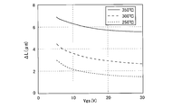
- FIG. 2 is a diagram showing the gate voltage dependence of the length of a ⁇ L region in the TFT shown in FIG.
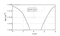
- FIG. 2 is a diagram showing a distribution of electron carrier concentration in a source / drain space in the TFT shown in FIG. 1.
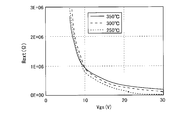
- 2 is a diagram showing the gate voltage dependence of the resistance value in the ⁇ L region in the TFT shown in FIG.
- FIG. (A)-(d) is a schematic cross section which shows a mode that the IGZO layer is reduce
- FIG. (A) is a plan view showing the configuration of the bottom gate TFT according to the first embodiment of the present invention
- (b) is a cross-sectional view along the line AA shown in (a).
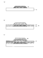
- FIGS. 7A to 7C are process cross-sectional views showing respective manufacturing processes of the TFT shown in FIGS. 7A and 7B.
- FIGS. FIGS. 7A to 7C are process cross-sectional views showing respective manufacturing processes of the TFT shown in FIGS. 7A and 7B.
- FIG. 8 is a diagram showing the gate voltage-drain current characteristics of the TFTs shown in FIGS. 7A and 7B.
- A) is a top view which shows the structure of the bottom gate type TFT which concerns on the 2nd Embodiment of this invention
- (b) is sectional drawing along the BB line of TFT shown to (a). .
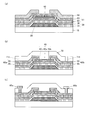
- FIGS. 14A to 14D are process cross-sectional views showing respective manufacturing processes of the TFT shown in FIGS. 14A and 14B.
- FIGS. FIGS. 14A to 14C are process cross-sectional views showing respective manufacturing processes of the TFT shown in FIGS. 14A and 14B.
- (A) And (b) is an expanded sectional view of the channel layer vicinity of TFT shown to Fig.14 (a) and FIG.14 (b).
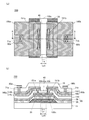
- (A) is a top view which shows the structure of the bottom gate type TFT which concerns on the 3rd Embodiment of this invention,
- (b) is sectional drawing along CC line of TFT shown to (a).
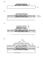
- FIGS. 18A to 18D are process cross-sectional views showing respective manufacturing processes of the TFT shown in FIGS.
- FIGS. 18A to 18C are process cross-sectional views showing respective manufacturing steps of the TFT shown in FIGS. 18A and 18B.
- FIG. 19 is an enlarged cross-sectional view showing a state in which the IGZO layer constituting the channel layer of the TFT shown in FIGS. 18A and 18B is reduced by heat treatment.
- FIG. 5 is a block diagram showing a configuration of a liquid crystal display device including any of the TFTs according to the first to third embodiments.
- FIG. 23 is a plan view showing a pattern arrangement in a pixel formation portion provided in the liquid crystal panel of the liquid crystal display device shown in FIG. 22.
- FIG. 1 is a cross-sectional view showing the configuration of the bottom gate TFT 10 used in the basic study.
- the TFT 10 includes a gate electrode 20 formed on an insulating substrate 15, a gate insulating film 30 formed so as to cover the gate electrode 20, and a gate insulating film 30 corresponding to the gate electrode 20.
- the island-shaped channel layer 40 formed at a position on the surface, the source electrode 60a extending from the left upper surface of the channel layer 40 to the left gate insulating film 30, and the gate insulation on the right side from the right upper surface of the channel layer 40
- a drain electrode 60 b extending on the film 30.
- the channel layer 40 is composed of an IGZO layer, and the IGZO layer is in contact with a titanium (Ti) electrode (not shown) included in the source electrode 60a and the drain electrode 60b.
- the titanium electrode reduces the IGZO layer by depriving oxygen which is one of the constituent elements from the IGZO layer, and is oxidized by the deprived oxygen. Further, hydrogen contained in the titanium electrode is supplied to the IGZO layer, and the supplied hydrogen diffuses inside the IGZO layer.
- the IGZO layer in which oxygen is taken away and hydrogen is diffused becomes a low resistance region, and the IGZO layer in which oxygen is not taken and hydrogen is not diffused remains as a high resistance region.
- low resistance regions also referred to as “first regions” 40 b are formed on both sides of the channel layer 40.
- a high resistance region (also referred to as “second region”) 40 a remains in the center of the channel layer 40 sandwiched between the two low resistance regions 40 b, and functions as a channel of the TFT 10.
- the size (length) of the high resistance region 40a or the low resistance region 40b by physical analysis or chemical analysis. Further, as will be described later, the size of the low resistance region 40b changes due to the measurement of the TFT characteristics, and the size of the high resistance region 40a also changes accordingly. Therefore, the channel length of the TFT 10 is obtained by the method described below.
- the length of the space between the end of the source electrode 60a and the end of the drain electrode 60b (hereinafter referred to as “source / drain space”) is Lch, and the TFT 10 obtained by measuring the TFT characteristics is obtained.
- the channel length (hereinafter referred to as “electrical channel length”) is Le
- a region of length ⁇ L represented by the following formula (1) is referred to as a ⁇ L region.
- ⁇ L Lch-Le (1)
- the resistance value Rmeas between the source / drain electrodes 60a and 60b is expressed by the following equation (2).
- Rmeas Vgs / Imeas (2)
- the drain current Imeas is a current having a channel width of 1 ⁇ m, and is a value obtained by dividing the total current flowing between the source / drain electrodes 60a and 60b by the channel width.
- the resistance value Rext obtained by subtracting the resistance value of the electrical channel length Le from the resistance value Rmeas between the source / drain electrodes 60a and 60b is mainly the resistance value in the ⁇ L region. Further, the resistance value Rext is the channel between the source electrode 60a and the drain electrode 60b and the channel. The contact resistance value with the layer 40 is also included.
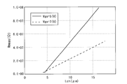
- FIG. 2 is a diagram showing the relationship between the length Lch of the space between the source / drain when the gate voltage is changed and the resistance value Rmeas between the source / drain electrodes 60a, 60b.
- FIG. 2 from data indicating the channel length dependence of TFT characteristics when 6 ⁇ 1V is applied to the gate electrode 20, a straight line when the gate voltage is 5V and a straight line when the gate voltage is 7V are shown. can get.
- the channel length component (horizontal axis component) at the intersection of two straight lines represents the length ⁇ L
- the resistance component vertical axis component
- FIG. 3 is a diagram illustrating the gate voltage dependence of the length ⁇ L of the ⁇ L region.
- the titanium electrodes included in the source electrode 60a and the drain electrode 60b take oxygen from the IGZO layer constituting the channel layer 40 by heat treatment, reduce the IGZO layer, and are oxidized by the taken oxygen. Further, hydrogen contained in the titanium electrode is supplied to the IGZO layer, and the supplied hydrogen diffuses into the IGZO layer. As a result, a region having a low resistance value is formed in the channel layer 40. This low resistance region is the ⁇ L region, and its length ⁇ L is determined by the deprived oxygen and the hydrogen diffused inside. As shown in FIG. 3, it can be seen that the length ⁇ L of the ⁇ L region becomes longer as the heat treatment temperature is higher.
- FIG. 4 is a graph showing the distribution of the electron carrier concentration Next in the source / drain space.
- the carrier concentration Next is the highest, and the electron carrier concentration Next becomes lower as it goes inside the space between the source and drain. Further, if the gate voltage applied to the gate electrode 20 is increased, the electron carrier concentration Next of the channel increases, and the electron carrier concentration Next in the ⁇ L region exceeds the concentration of the low region.
- the ⁇ L region is only a region having a high electron carrier concentration Next, and its length ⁇ L decreases.
- the electrical channel length Le is increased, and the length ⁇ L of the ⁇ L region is decreased.
- FIG. 5 is a diagram showing the gate voltage dependence of the resistance value Rext in the ⁇ L region.
- the resistance value Rext is decreased. If the gate voltage increases, the region where the electron carrier concentration Next inside the ⁇ L region is low changes to a channel, and the region involved in the resistance value of the ⁇ L region is only the region where the electron carrier concentration Next in the ⁇ L region is high. Because it becomes. In the region where the gate voltage is high, the resistance value Rext increases as the heat treatment temperature increases. This is because the length ⁇ L of the ⁇ L region becomes longer as the temperature of the heat treatment is higher.
- the length ⁇ L of the ⁇ L region depends on the gate voltage. Of the ⁇ L region, the contribution to the drain current Imeas when the TFT 10 is in the ON state is not the region inside the channel where the electron carrier concentration Next is low, but the region close to the ends of the source electrode 60a and the drain electrode 60b. . Therefore, the length ⁇ L of the ⁇ L region in this specification is defined as a length obtained from FIG. 3 when 20 to 30 V is applied to the gate electrode 20.
- the low resistance region 40b shown in FIG. 1 is a ⁇ L region, that is, a region having a length of ⁇ L
- the high resistance region 40a is a region obtained by removing the low resistance region 40b from the space between the source and drain, that is, the length.
- the IGZO layer included in the channel layer 40 is deprived of oxygen and reduced by heat treatment, and the titanium electrode deprived of oxygen is oxidized. Further, hydrogen contained in the titanium electrode is supplied to the IGZO layer. The supplied hydrogen diffuses inside the IGZO layer. By such reduction of the IGZO layer and diffusion of hydrogen, a low resistance region 40b having a length ⁇ L is formed.
- a titanium electrode 65 is formed on the IGZO layer 45.
- the IGZO layer 45 is not reduced.
- the oxygen concentration of the IGZO layer 45 is high and the oxygen concentration of the titanium electrode 65 is low, the oxygen concentration gradient is steep at the interface between the IGZO layer 45 and the titanium electrode 65.
- oxygen contained in the IGZO layer 45 in the space between the source and drain away from the interface is sequentially supplied to the interface and taken away by the titanium electrode 65.
- the titanium electrode 65 is oxidized by oxygen taken from the IGZO layer 45.
- the titanium electrode 65 takes oxygen not only from the IGZO layer 45 below but also from the IGZO layer 45 in the space between the source and drain, and reduces it.
- hydrogen is supplied from the titanium electrode 65 and diffuses into the IGZO layer 45. For this reason, the low resistance region 40b extends to the IGZO layer 45 in the source / drain space.
- the unreduced IGZO layer 45 remains as the high resistance region 40a.
- the low resistance region is formed by depriving oxygen and being reduced, and description of the diffusion of hydrogen supplied from the titanium electrode is omitted.
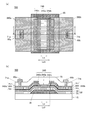
- FIG. 7A is a plan view showing the configuration of the bottom-gate TFT 100 according to the first embodiment of the present invention, and FIG. 7B is along the line AA shown in FIG. It is sectional drawing.
- the TFT 100 illustrated in FIGS. 7A and 7B is also referred to as a channel-etched TFT. With reference to FIG. 7A and FIG. 7B, the configuration of the TFT 100 will be described.
- a gate electrode 20 is formed on an insulating substrate 15 such as a glass substrate.
- the gate electrode 20 is composed of a laminated metal film in which a copper (Cu) film is laminated on a titanium film, for example.
- the gate electrode 20 may be formed of a laminated metal film in which a titanium film, an aluminum (Al) film, and a titanium film are sequentially laminated from the insulating substrate 15 side.
- a gate insulating film 30 is formed so as to cover the entire insulating substrate 15 including the gate electrode 20.
- the gate insulating film 30 is composed of a laminated insulating film in which a silicon oxide (SiO 2) film 36 is laminated on a silicon nitride (SiNx) film 35.
- SiO 2 silicon oxide
- SiNx silicon nitride
- An island-shaped channel layer 40 is formed at a position on the surface of the gate insulating film 30 corresponding to the gate electrode 20.
- the channel layer 40 is composed of an IGZO layer containing indium (In), gallium (Ga), zinc (Zn), and oxygen (O).
- Low resistance regions 40b are formed on both sides of the channel layer 40, respectively. In the center of the channel layer 40 sandwiched between the two low resistance regions 40b, a high resistance region 40a having a resistance value higher than that of the low resistance region 40b remains.
- the film thickness of the IGZO layer is preferably about 30 to 50 nm. This is due to the following reason. When the film thickness of the IGZO layer becomes thinner than 30 ⁇ m, the TFT characteristics of the TFT 100 become unstable, and a threshold voltage shift occurs due to temperature and gate voltage stress. On the other hand, when the film thickness is thicker than 50 nm, the controllability by the gate voltage is deteriorated, and the leakage current (particularly when the gate voltage is 0 V) increases.
- the composition ratio of the IGZO layer used in the present embodiment is represented by the following formula (4).
- Indium: gallium: zinc 1: 1: 1 (4)
- the composition ratio of the IGZO layer may be a case represented by the following formula (5) or may be another composition ratio.
- Indium: gallium: zinc 4: 5: 1 (5)
- the IGZO layer used in this embodiment is most preferably an amorphous film, but may be a crystalline film such as a microcrystalline film or a polycrystalline film. In the case of a microcrystalline film, the on-resistance of the TFT 100 is reduced and the current driving force is increased.
- an oxide semiconductor that can be used as the channel layer 40 of the TFT 100 is not limited to IGZO, but may be an In—Zn—O system, an In—Zn—Sn—O system, an In—Zn—Si—O system, or the like. May be. Specifically, IZO, ITO, ZnO, SnO, WO, IO or the like may be used.
- a source electrode 60a and a drain electrode 60b formed at a predetermined distance on the upper surface of the channel layer 40 are disposed.
- the source electrode 60 a is formed to extend from the upper left surface of the channel layer 40 to the left gate insulating film 30.
- the drain electrode 60 b is formed so as to extend from the right upper surface of the channel layer 40 to the right gate insulating film 30.
- the ends of the source electrode 60a and the drain electrode 60b are formed so as to be positioned on the left and right low resistance regions 40b, respectively.
- the source electrode 60a and the drain electrode 60b are made of, for example, a laminated metal film in which a copper electrode 66 having a thickness of 300 to 1000 nm is laminated on a titanium electrode 65 having a thickness of 100 nm.
- the source electrode 60a and the drain electrode 60b are formed of the laminated metal film because the resistance value of the titanium electrode 65 is high. This is to reduce the resistance value of 60b.
- the titanium electrode 65 is included in the source electrode 60a and the drain electrode 60b for the following reason. That is, titanium has a high ability to take oxygen from an oxide semiconductor (especially IGZO) and reduce it, so that the low resistance region 40b is easily formed.
- the resistance value of the source electrode 60a and the drain electrode 60b may be high, the source electrode 60a and the drain electrode 60b may be composed of only the titanium electrode 65.
- the source electrode 60a and the drain electrode 60b are formed of a single layer metal film such as titanium, aluminum, copper, tungsten (W), molybdenum (Mo), and tantalum (Ta), aluminum-neodymium (Nd), titanium-aluminum, molybdenum.
- a single layer metal film such as titanium, aluminum, copper, tungsten (W), molybdenum (Mo), and tantalum (Ta), aluminum-neodymium (Nd), titanium-aluminum, molybdenum.
- -Laminated metal in which a single layer alloy film of tungsten, indium-tin, titanium film, aluminum film, titanium film is laminated in order, an aluminum film is laminated on the titanium film, or a molybdenum film is laminated on the titanium film
- An electrode made of a film or the like may be used.
- the end of the source electrode 60 a is disposed above the left side of the gate electrode 20, and the end of the drain electrode 60 b is disposed above the right side of the gate electrode 20. For this reason, when a predetermined voltage is applied to the gate electrode 20, electrons are induced in each low resistance region 40 b of the channel layer 40 by the electric field from the gate electrode 20, thereby forming a high concentration carrier layer. By forming the high concentration carrier layer, the source electrode 60a and the drain electrode 60b are ohmically connected to the two low resistance regions 40b, respectively.
- a passivation film 70 is formed so as to cover the entire insulating substrate 15 including the source electrode 60a and the drain electrode 60b.
- the passivation film 70 is made of a silicon oxide film having a thickness of 300 nm.
- contact holes 71a and 71b reaching the surfaces of the source electrode 60a and the drain electrode 60b are opened, respectively.
- the source electrode 60a and the drain electrode 60b are electrically connected to external wirings 80a and 80b formed on the passivation film 70 via contact holes 71a and 71b, respectively.
- the electrical channel length Le is shorter than the length Lch of the space between the source and drain.
- the electrical channel length Le is shorter by about 1 to 3 ⁇ m than the length Lch of the source / drain space.
- the TFT 100 operates normally even when the source / drain space is narrowed to the resolution limit by making the electrical channel length Le shorter by 1 to 3 ⁇ m than the length Lc of the source / drain space.
- the electrical channel length Le shown in FIGS. 7A and 7B shows the channel length of the TFT 100 when 20 to 30 V is applied to the gate electrode 20.
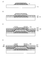
- FIGS. 9 (a) to 9 (c) are process cross-sectional views showing respective manufacturing steps of the TFT 100 shown in FIGS. 7 (a) and 7 (b). .
- a titanium film (not shown) and a copper film (not shown) are successively formed on the insulating substrate 15 by using, for example, a sputtering method.
- a resist pattern (not shown) is formed on the surface of the copper film using a photolithography method.
- the resist pattern is peeled off. Thereby, the gate electrode 20 in which the copper film is layered on the titanium film is formed.
- nitridation is performed by using a plasma chemical vapor deposition method (hereinafter referred to as “plasma CVD method”) so as to cover the entire insulating substrate 15 including the gate electrode 20.
- plasma CVD method a plasma chemical vapor deposition method
- a silicon film 35 and a silicon oxide film 36 are successively formed to form a gate insulating film 30.
- an IGZO film 41 containing indium, gallium, zinc and oxygen is formed on the surface of the gate insulating film 30 by a sputtering method.
- the IGZO film 41 is formed by a direct current (DC) sputtering method using a target in which indium oxide (In 2 O 3), gallium oxide (Ga 2 O 3), and zinc oxide (ZnO) are mixed and equimolarly sintered.
- the thickness of the IGZO film 41 is 30 to 50 nm.
- a resist pattern 48 is formed on the surface of the IGZO film 41.
- the IGZO film 41 is etched by dry etching using the resist pattern 48 as a mask, and the resist pattern 48 is peeled off. Thereby, an IGZO layer to be the island-shaped channel layer 40 is formed at a position corresponding to the gate electrode 20 on the gate insulating film 30.
- heat treatment is performed for 1 hour at a temperature of 350 ° C. in the atmosphere.
- the film quality of the gate insulating film 30 such as the silicon oxide film 36 is improved, and the shift amount of the threshold voltage due to the temperature stress and the gate voltage stress can be suppressed. Further, since defects at the interface between the silicon oxide film 36 and the channel layer 40 are reduced, the rising characteristics of the TFT 100 can be improved.
- the heat treatment is performed before forming the source electrode 60a and the drain electrode 60b, it is not necessary to consider the reduction of the IGZO layer by the titanium electrode 65. Heat treatment becomes possible.
- a source metal film 61 is formed using a sputtering method.
- the source metal film 61 is composed of a laminated metal film in which a copper film 63 having a thickness of 300 to 1000 nm is laminated on a titanium film 62 having a thickness of 30 to 100 nm.
- a copper film 63 having a thickness of 300 to 1000 nm is laminated on a titanium film 62 having a thickness of 30 to 100 nm.
- a resist pattern 68 is formed on the source metal film 61 by using a photolithography method so as to be separated left and right above the gate electrode 20 by a predetermined distance. Since the predetermined distance formed in the resist pattern 68 is shorter than the length of the gate electrode 20, the end portions of the resist pattern 68 are formed so as to overlap the left and right side portions of the gate electrode 20, respectively.
- the copper film 63 and the titanium film 62 of the source metal film 61 are sequentially etched by wet etching using the resist pattern 68 as a mask, and the titanium electrode 65 and the copper electrode 66 are laminated.
- a source electrode 60a and a drain electrode 60b are formed.
- the source electrode 60 a extends from the left upper surface of the channel layer 40 to the left gate insulating film 30.
- the drain electrode 60 b extends from the right upper surface of the channel layer 40 to the right gate insulating film 30. Note that no etching stopper layer is formed on the channel layer 40.
- the source metal film 61 is etched by the wet etching method, the channel layer 40 is hardly reduced when the source electrode 60a and the drain electrode 60b are formed.
- a silicon oxide film to be the passivation film 70 is formed by plasma CVD so as to cover the entire insulating substrate 15 including the source electrode 60a and the drain electrode 60b. Since the passivation film 70 is in direct contact with the channel layer 40, it is preferable to use a silicon oxide film that hardly reduces the IGZO layer constituting the channel layer 40 as the passivation film 70.
- this heat treatment can recover the damage generated in the source electrode 60a and the drain electrode 60b when the contact holes 71a and 71b are etched. Furthermore, since oxygen contained in the passivation film 70 is supplied to the high resistance region 40a of the channel layer 40, the high resistance region 40a can maintain a high resistance value.
- the temperature and time of the heat treatment are determined in consideration of the film thickness of the titanium film 62 and the power at the time of film formation, and details thereof will be described later.
- a metal film (not shown) is formed on the passivation film 70 including the contact holes 71a and 71b, and the metal film is patterned using a resist pattern (not shown) as a mask. Thereby, external wirings 80a and 80b electrically connected to the source electrode 60a and the drain electrode 60b through the contact holes 71a and 71b are formed.
- the heat treatment is performed before the source metal film 61 is formed and after the contact holes 71a and 71b are formed.
- the heat treatment before forming the source metal film 61 may be omitted, and the heat treatment may be performed collectively after the contact holes 71a and 71b are formed.
- the heat treatment is performed after the contact holes 71a and 71b are formed, the reduction of the IGZO layer by the titanium electrode 65 proceeds, so that the heat treatment for a long time cannot be performed at a high temperature. For this reason, it is difficult to sufficiently improve the TFT characteristics.
- the manufacturing process of the TFT 100 can be simplified.
- the length ⁇ L of the low resistance region 40b determined by the reduction of the IGZO film 41 by the titanium film 62 is the film thickness of the titanium film 62, the power when the titanium film 62 is formed by sputtering, and after the film formation of the titanium film 62. It was found that the heat treatment conditions (temperature and time) (for example, after the formation of the contact holes 71a and 71b) are greatly affected. Therefore, an experiment was conducted to examine the relationship between these process conditions and the length ⁇ L of the low resistance region 40b.
- FIG. 10 is a diagram showing the relationship between various process conditions and the length ⁇ L of the low resistance region 40b. Note that the length Lch of the source / drain space of the TFT used in the experiment is 5 ⁇ m.
- the film thickness of the titanium film 62 was set to 30 nm or 70 nm, and the power during film formation by the sputtering method was set to either 2 kW or 7 kW. Further, the heat treatment after the formation of the titanium film 62 was carried out by changing the temperature in the range of 250 to 350 ° C. in the atmosphere, and the processing time was 1 hour in any case. Experiments were performed by combining these process conditions.
- the thickness of the titanium film 62 was 100 nm, the power was 2 kW, and heat treatment was performed at 350 ° C. for 1 hour. At this time, the length ⁇ L of the low resistance region 40b was 0 ⁇ m. Therefore, the electrical channel length Le of the TFT 101 is 5 ⁇ m, which is the same as the length Lch of the source / drain space, and the electrical channel length Le cannot be shortened.
- FIG. 11 is a cross-sectional view of the TFT 101 manufactured under the process conditions of Experiment 1.
- the same components as those of the TFT 100 shown in FIG. 7B are denoted by the same reference numerals, and the description thereof is omitted.
- the length ⁇ L of the low resistance region 40b is 0 ⁇ m, and the length Lch of the space between the source / drain and the electrical channel length Le match. For this reason, the electrical channel length Le is determined by the resolution limit of the exposure apparatus and cannot be shorter than that.
- the thickness of the titanium film 62 was 30 nm, the power was 7 kW, and heat treatment was performed at 350 ° C. for 1 hour. At this time, the length ⁇ L of the low resistance region 40b was 5 ⁇ m. In this case, the electrical channel length Le of the TFT was 0 ⁇ m, and the TFT 102 was always in a conductive state.
- FIG. 12 is a cross-sectional view of the TFT 102 manufactured under the process conditions of Experiment 2.
- the same components as those of the TFT 100 shown in FIG. 7B are denoted by the same reference numerals, and the description thereof is omitted.
- the TFT 102 in the channel layer 40 of the TFT 102, the high resistance region disappears and the whole becomes the low resistance region 40b. For this reason, the TFT 102 is always in a conductive state, and the function as a transistor is lost.
- the titanium film 62 was 30 nm thick, the power was 7 kW, and heat treatment was performed at 300 ° C. for 1 hour. At this time, the length ⁇ L of the low resistance region 40b was 3 ⁇ m. In this case, the electrical channel length Le of the TFT was 2 ⁇ m, and it was found that the TFT operates normally.
- the titanium film 62 was 70 nm thick, the power was 7 kW, and heat treatment was performed at 300 ° C. for 1 hour. At this time, the length ⁇ L of the low resistance region 40b was 2 ⁇ m. In this case, the electrical channel length Le of the TFT was 3 ⁇ m, and it was found that the TFT operates normally. From the results of Experiment 3 and Experiment 4, it was found that if the thickness of the titanium film 62 is increased, the length ⁇ L of the low resistance region 40b is shortened and the electrical channel length Le is increased.
- the titanium film 62 was 70 nm thick, the power was 7 kW, and heat treatment was performed at 250 ° C. for 1 hour. At this time, the length ⁇ L of the low resistance region 40b was 1 ⁇ m. In this case, the electrical channel length Le of the TFT was 4 ⁇ m, and it was found that the TFT operates normally. Further, from the results of Experiment 4 and Experiment 5, it was found that when the heat treatment temperature is lowered, the length ⁇ L of the low resistance region 40b is shortened and the electrical channel length Le is lengthened.
- the TFT operates normally when the length ⁇ L of the low resistance region 40b is 1 to 3 ⁇ m. Therefore, the electrical channel length Le is preferably shorter by about 1 to 3 ⁇ m than the length Lch of the space between the source / drain.
- the length ⁇ L of the low resistance region 40b is mainly determined by the thickness of the titanium film 62 and the power at the time of film formation.
- the length ⁇ L of the low resistance region 40b is the shortest and the electrical channel length Le is the longest. In this way, by adjusting the film thickness and power of the titanium film 62, the length of the high resistance region 40a can be made shorter than the resolution limit of the exposure apparatus, so that a thin film transistor having a large current driving capability is formed. Can do.
- the heat treatment time is 1 hour, but it may be 0.5 hours or more and 3 hours or less.
- the variation in the length ⁇ L of the low resistance region 40b is suppressed, so that the variation in the electrical channel length Le is also suppressed.
- the threshold voltage shift due to the gate voltage stress cannot be sufficiently suppressed.
- the throughput deteriorates.
- the heat treatment is performed at a temperature lower than 250 ° C.
- the threshold voltage shift cannot be suppressed, and the low resistance region 40b is hardly formed.
- the heat treatment is performed at a temperature higher than 350 ° C., the variation in the length ⁇ L of the low resistance region 40b increases, and thus the variation in the electrical channel length Le increases.
- Experiment 6 is an experimental result of the TFT 200 according to the second embodiment described later, and will be described in the second embodiment.
- FIG. 13 is a diagram showing the gate voltage-drain current characteristics of the TFT 100 shown in FIGS. 7A and 7B.
- the TFT 100A is a TFT with a low resistance region 40b length ⁇ L of 2 ⁇ m
- the TFT 100B is a TFT with a low resistance region 40b length ⁇ L of 0 ⁇ m
- the TFT 100C has a low resistance region 40b length ⁇ L of 4. .5 ⁇ m TFT.
- the length Lch of the space between the source / drain of the TFTs 100A to 100C is 4.5 ⁇ m.
- TFT100A was heat-treated at 300 ° C. for 1 hour.
- the electrical channel length Le is 2.5 ⁇ m.
- the thickness of the titanium electrode 65 directly in contact with the IGZO layer constituting the channel layer 40 is 100 nm, and heat treatment is performed at 250 ° C. for 1 hour.
- the electrical channel length Le remains 4.5 ⁇ m.
- the electrical channel length Le is 0 ⁇ m.
- the drain current Ids of the TFT 100A is 1.8 times larger than the drain current Ids of the TFT 100B. This is considered because the electrical channel length Le of the TFT 100A is shorter by 2.0 ⁇ m than the electrical channel length Le of the TFT 100B. From this, it can be seen that by controlling the length ⁇ of the low-resistance region 40b, the electrical channel length Le can be adjusted, and the TFT 100A with excellent current driving capability can be manufactured. In the TFT 100C, the electrical channel length Le is 0 ⁇ m, which means that the drain current Ids cannot be controlled by the gate voltage.
- FIG. 14A is a plan view showing a configuration of a bottom-gate TFT 200 according to the second embodiment of the present invention
- FIG. 14B is a BB line of the TFT 200 shown in FIG. FIG.
- the TFT 200 shown in FIGS. 14A and 14B is also referred to as an etch stopper TFT.
- a gate electrode 20 is formed on an insulating substrate 15 such as a glass substrate.
- a gate insulating film 30 is formed so as to cover the entire insulating substrate 15 including the gate electrode 20. Note that the configuration of the gate electrode 20 and the gate insulating film 30 is the same as that of the TFT 100 according to the first embodiment, and therefore, the same reference numerals are given and description thereof is omitted.
- An island-shaped channel layer 40 is formed at a position on the surface of the gate insulating film 30 corresponding to the gate electrode 20.
- the channel layer 40 is made of an IGZO layer.
- the channel layer 40 includes a low resistance region 40b formed on both sides thereof, and a high resistance region 40a left in the center of the channel layer 40 sandwiched between the two low resistance regions 40b. Note that the film thickness, crystallinity, composition ratio, and the like of the IGZO layer are the same as those of the TFT 100 according to the first embodiment, and a description thereof will be omitted.
- an etching stopper layer 150 is formed on the channel layer 40 and the gate insulating film 30.
- the etching stopper layer 150 has a function of protecting the surface of the channel layer 40 from being etched when a source electrode 160a and a drain electrode 160b described later are formed by etching, and reducing the load capacity of the wiring. For this reason, the thickness of the etching stopper layer 150 is preferably thick, but if it is too thick, there is a problem that the film formation time becomes long and the throughput decreases. Therefore, the preferable film thickness of the etching stopper layer 150 is 100 to 500 nm. Further, the etching stopper layer 150 is formed of a silicon oxide film in order to make it difficult to take oxygen from the IGZO layer that constitutes the channel layer 40 that is in direct contact therewith.
- etching stopper layer 150 In the etching stopper layer 150, contact holes 151a and 151b reaching the low resistance region 40b of the channel layer 40 are opened.
- a source electrode 160a and a drain electrode 160b formed at a predetermined distance are disposed on the upper surface of the etching stopper layer 150c sandwiched between the contact holes 151a and 151b.
- the source electrode 160a is formed so as to extend from the left upper surface of the etching stopper layer 150c to the left gate insulating film 30, and is electrically connected to the low resistance region 40b of the channel layer 40 via the contact hole 151a. It is connected to the.
- the drain electrode 160b is formed to extend from the right upper surface of the etching stopper layer 150c to the right gate insulating film 30, and is electrically connected to the low resistance region 40b of the channel layer 40 via the contact hole 151b. It is connected to the. Note that the film thickness and material of the source electrode 160a and the drain electrode 160b are the same as those of the TFT 100, and thus description thereof is omitted.
- the end of the source electrode 160a is disposed on the upper left surface of the etching stopper layer 150c, and the end of the drain electrode 160b is disposed on the upper right surface of the etching stopper layer 150c. Therefore, as in the case of the TFT 100, when a gate voltage is applied to the gate electrode 20, electrons are induced in the low resistance region 40b, and a high concentration carrier layer is formed. By forming the high concentration carrier layer, the source electrode 160a and the drain electrode 160b are ohmically connected to the two low resistance regions 40b, respectively.
- a passivation film 70 is formed so as to cover the entire insulating substrate 15 including the source electrode 60a and the drain electrode 60b.
- the passivation film 70 is made of a silicon oxide film having a thickness of 300 nm.
- contact holes 71a and 71b reaching the surfaces of the source electrode 60a and the drain electrode 60b are opened, respectively.
- the source electrode 60a and the drain electrode 60b are electrically connected to external wirings 80a and 80b formed on the passivation film 70 via contact holes 71a and 71b, respectively.
- the electrical channel length Le is shorter than the length Lch of the space between the source and drain. As in the case of the TFT 100, the electrical channel length Le is preferably shorter by about 1 to 3 ⁇ m than the length Lch of the source / drain space.
- the TFT 200 operates normally even when the source / drain space is narrowed to the resolution limit by making the electrical channel length Le shorter by 1 to 3 ⁇ m than the length Lc of the source / drain space. Note that the electrical channel length Le shown in FIGS. 14A and 14B shows the channel length of the TFT 200 when 20 to 30 V is applied to the gate electrode 20.
- FIGS. 16 (a) to 16 (c) are process cross-sectional views showing respective manufacturing steps of the TFT 200 shown in FIGS. 14 (a) and 14 (b). .
- FIGS. 15A to 15C are denoted by the same reference numerals as those in FIGS. 8A to 8C, and description thereof is omitted.
- a silicon oxide film 151 having a thickness of 100 to 500 nm is formed by covering the channel layer 40 using a plasma CVD method.
- a resist pattern 158 is formed on the silicon oxide film 151.
- the silicon oxide film 151 is etched by dry etching to form an etching stopper layer 150 in which contact holes 151a and 151b reaching the surface of the channel layer 40 are formed.
- a portion of the etching stopper layer 150 sandwiched between the contact holes 151a and 151b is particularly referred to as an etching stopper layer 150c.
- heat treatment is performed at 350 ° C. for 1 hour.
- the purpose of this heat treatment is to improve the reliability, such as suppressing the threshold voltage shift due to gate voltage stress, and to improve the TFT characteristics by recovering the damage caused to the IGZO layer during contact etching.
- the contact holes 151a and 151b are opened, and before the source metal film 161 described later is formed.
- a source metal film 161 is formed on the etching stopper layer 150 including the contact holes 151a and 151b by using a sputtering method. Since the configuration, film thickness, and film formation conditions of the source metal film 161 are the same as those of the source metal film 61 of the TFT 100, description thereof is omitted.
- a resist pattern 168 is formed on the source metal film 161 by using a photolithography method so as to be separated left and right above the etching stopper layer 150 by a predetermined distance.
- the copper film 162 and the titanium film 163 included in the source metal film 161 are sequentially etched using the dry etching method, and the titanium electrode 165 and the copper electrode are then etched.
- a source electrode 160a and a drain electrode 160b constituted by 166 are formed.
- the source electrode 160a extends from the upper left surface of the etching stopper layer 150c to the left gate insulating film 30, and is also electrically connected to the channel layer 40 through the contact hole 151a.
- the drain electrode 160b extends from the right upper surface of the etching stopper layer 150c to the right gate insulating film 30, and is also electrically connected to the channel layer 40 through the contact hole 151b. Note that the positional relationship between the source electrode 160a and the drain electrode 160b and the gate electrode 20 is the same as that of the TFT 100, and thus the description thereof is omitted.
- the formation of the passivation film 70 shown in FIG. 16C to the formation of the external wirings 80a and 80b is the same as that of the TFT 100 except for the heat treatment after the formation of the contact holes 71a and 71b, description thereof is omitted. To do.
- the low resistance region 40b is formed on both sides of the channel layer 40, and the high resistance region 40a remains in the center of the channel layer 40 sandwiched between the two low resistance regions 40b. In this way, the TFT 200 shown in FIGS. 14A and 14B is formed.
- FIG. 17A and FIG. 17B are enlarged cross-sectional views in the vicinity of the channel layer 40 of the TFT 200.
- a titanium electrode 165 included in the source electrode 160a and the drain electrode 160b is formed on the etching stopper layer 150.
- the titanium electrode 165 is electrically connected to the IGZO layer 45 constituting the channel layer 40 through contact holes 151 a and 151 b formed in the etching stopper layer 150.
- a voltage is applied to the titanium electrode 165, electrons are induced at the position of the IGZO layer 45 corresponding to the titanium electrode 165 by the electric field.
- a high concentration carrier layer is formed at the position of the IGZO layer 45 corresponding to the titanium electrode 165 on the etching stopper layer 150.
- the IGZO layer 45 immediately below the etching stopper layer 150c is located away from the positions of the contact holes 151a and 151b. Therefore, as shown in FIG. 17B, it is necessary to raise the temperature of the heat treatment and move the oxygen contained in the IGZO layer 45b in the source / drain space to the titanium electrode 165 and take it away. The IGZO layer 45b deprived of oxygen in this way becomes the low resistance region 40b.
- the electrical channel length Le becomes shorter than the length Lch of the space between the source and drain.
- the electrical channel length Le is 2.5 ⁇ m. From this, it can be seen that when a gate voltage is applied to the TFT 200, low resistance regions 40b each having a length of 2.5 ⁇ m are formed in the IGZO layer 45 located immediately below both ends of the etching stopper layer 150c. As a result, the electrical channel length Le can be shortened by 2 ⁇ m compared to the case shown in Experiment 1 of FIG.
- the current driving capability of the TFT 200 can be increased as in the case of the TFT 100 according to the first embodiment.
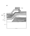
- FIG. 18A is a plan view showing a configuration of a bottom-gate TFT 300 according to the third embodiment of the present invention
- FIG. 18B is a CC line of the TFT 300 shown in FIG. FIG.
- the TFT 300 illustrated in FIGS. 18A and 18B is also referred to as a bottom contact TFT.
- a gate electrode 20 is formed on the insulating substrate 15.
- a gate insulating film 30 is formed so as to cover the entire insulating substrate 15 including the gate electrode 20. Note that the configuration of the gate electrode 20 and the gate insulating film 30 is the same as that of the TFT 100 according to the first embodiment, and therefore, the same reference numerals are given and description thereof is omitted.
- a source electrode 260a and a drain electrode 260b formed at a predetermined distance are formed on the gate insulating film 30 above the gate electrode 20, a source electrode 260a and a drain electrode 260b formed at a predetermined distance are formed.
- the source electrode 260 a and the drain electrode 260 b are configured by a laminated metal film in which a titanium electrode 265, a copper electrode 266, and a titanium electrode 267 are sequentially laminated on the surface of the gate insulating film 30.
- the end portions of the copper electrode 266 and the titanium electrode 267 are set back to the left from the end portions of the titanium electrode 265.
- the drain electrode 260 b the end portions of the copper electrode 266 and the titanium electrode 267 are set back to the right side from the end portions of the titanium electrode 265.
- a channel layer 240 made of an IGZO layer is formed on the gate insulating film 30 sandwiched between the source electrode 260a and the drain electrode 260b.
- One end of the channel layer 240 extends to the upper surface of the source electrode 260a, and the other end extends to the upper surface of the drain electrode 260b.
- One end of the channel layer 40 in contact with the source electrode 260a and the other end of the channel layer 40 in contact with the drain electrode 260b are in direct contact with the titanium electrode 265 and the titanium electrode 267. Therefore, a low resistance region (also referred to as “first region”) 240 b reduced by the titanium electrode 265 and the titanium electrode 267 is formed on both sides of the channel layer 240. In the center of the channel layer 40 sandwiched between the two low resistance regions 240b, a high resistance region (also referred to as "second region”) 240a that has not been reduced remains.
- the end of the source electrode 260a is disposed above the left side of the gate electrode 20, and the end of the drain electrode 260b is disposed above the right side of the gate electrode 20. For this reason, when a predetermined voltage is applied to the gate electrode 20, electrons are induced in each low resistance region 240 b of the channel layer 240 by the electric field from the gate electrode 20, thereby forming a high concentration carrier layer. By forming the high concentration carrier layer, the source electrode 260a and the drain electrode 260b are ohmically connected to the two low resistance regions 240b, respectively.
- a passivation film 70 is formed so as to cover the entire insulating substrate 15 including the source electrode 260a and the drain electrode 260b.
- the passivation film 70 is made of a silicon oxide film having a thickness of 300 nm.
- contact holes 71a and 71b reaching the surfaces of the source electrode 260a and the drain electrode 260b are opened, respectively.
- the source electrode 60a and the drain electrode 60b are electrically connected to external wirings 80a and 80b formed on the passivation film 70 via contact holes 71a and 71b, respectively.
- the electrical channel length Le is shorter than the length Lch of the space between the source and drain.
- the electrical channel length Le is preferably shorter by about 1 to 3 ⁇ m than the length Lch of the source / drain space. Even if the source / drain space is narrowed to the resolution limit by making the electrical channel length Le shorter by 1 to 3 ⁇ m than the length Lc of the source / drain space, the TFT 300 operates normally. Note that the electrical channel length Le shown in FIGS. 18A and 18B shows the channel length of the TFT 300 when 20 to 30 V is applied to the gate electrode 20.
- FIGS. 19A and 19B are denoted by the same reference numerals as those in FIGS. 8A and 8B, and description thereof is omitted.
- a source metal film 261 is formed on the gate insulating film 30 by using a sputtering method.
- the source metal film 261 is a laminated metal film in which a titanium film 262, a copper film 263, and a titanium film 264 are laminated in this order.
- a resist pattern 268 is formed on the source metal film 261 by using a photolithography method so as to be separated left and right above the gate electrode 20 by a predetermined distance.
- the titanium film 264 and the copper film 263 included in the source metal film 261 are sequentially etched using the wet etching method, and the titanium electrode 267 and the copper electrode included in the source electrode 260a and the drain electrode 260b are etched. 266 is formed.
- the resist pattern 268 is peeled off, the titanium electrode 267 and the copper electrode 266 are covered, and a resist pattern 269 having an opening narrower than the resist pattern 268 is formed.
- the titanium film 262 is etched by wet etching to form a titanium electrode 265.
- the source electrode 260a and the drain electrode 260b have a structure having stepped steps in which the ends of the titanium electrode 267 and the copper electrode 266 are set back from the ends of the titanium electrode 265.
- the source electrode 260 a extends from the upper left to the left of the gate electrode 20, and the drain electrode 260 b extends from the upper right to the right of the gate electrode 20. Note that the positional relationship between the end portions of the source electrode 260a and the drain electrode 260b and the side portions of the gate electrode 20 is the same as that of the TFT 100, and thus description thereof is omitted.
- an IGZO film (not shown) having a film thickness of 30 to 50 nm is formed by sputtering.
- a channel layer 240 made of an IGZO layer is formed in the source / drain space.
- One end of the channel layer 240 extends to the upper surface of the source electrode 260a, and the other end extends to the upper surface of the drain electrode 260b.
- the lower left surface of the IGZO layer is in direct contact with the end surfaces of the titanium electrode 267 and the titanium electrode 265 included in the source electrode 260a, and the lower right surface of the IGZO layer is the titanium electrode 267 and the titanium included in the drain electrode 260b. It is in direct contact with the surface of the end portion of the electrode 265.
- a passivation film 70 is formed so as to cover the entire insulating substrate 15 including the channel layer 240, the source electrode 260a, and the drain electrode 260b.
- contact holes 71a and 71b reaching the surfaces of the source electrode 260a and the drain electrode 260b are formed in the passivation film 70, respectively. Since these steps are the same as those in the first embodiment, detailed description thereof is omitted.
- heat treatment is performed in the atmosphere at a temperature of 350 ° C. and for a time of 1 hour.
- oxygen moves from the IGZO layer constituting the channel layer 240 to the titanium electrodes 265 and 267 of the source electrode 260a and the drain electrode 260b, and the IGZO layer is reduced.
- the low resistance region 240b is formed on both sides of the channel layer 240, and the IGZO layer sandwiched between the two low resistance regions 240b remains as the high resistance region 240a.
- the damage generated in the source electrode 260a and the drain electrode 260b due to the etching of the contact holes 71a and 71b is recovered, and the TFT characteristics are improved.
- the manner in which the IGZO layer is reduced will be described later.
- the formation of the passivation film 70 shown in FIG. 20C to the formation of the external wirings 80a and 80b is the same as that of the TFT 100 except for the heat treatment after the contact holes 71a and 71b are formed, the description thereof is omitted. To do.
- the heat treatment after the contact holes 71a and 71b are formed the low resistance region 240b is formed on both sides of the channel layer 240, and the high resistance region 240a remains in the center of the channel layer 240 sandwiched between the two low resistance regions 240b. In this way, the TFT 300 shown in FIGS. 18A and 18B is formed.
- FIG. 21 is an enlarged cross-sectional view of the TFT 300 showing how the IGZO layer constituting the channel layer 240 is reduced by heat treatment.
- the IGZO layer constituting the channel layer 240 is in direct contact with the surfaces and side surfaces of the titanium electrodes 265 and 267 of the source electrode 260a.
- the heat treatment the IGZO layer is reduced from the regions directly in contact with the surfaces and side surfaces of the titanium electrodes 265 and 267, so that the low resistance region 240b spreads from the region in contact with the titanium electrodes 265 and 267 as a base point.
- the current driving capability of the TFT 300 can be increased as in the case of the TFT 100 according to the first embodiment.
- the source electrode 260a and the drain electrode 260b are configured by a laminated metal film in which a titanium electrode 265, a copper electrode 266, and a titanium electrode 267 are laminated in order.
- the laminated metal film only needs to include at least one of the titanium electrode 265 and the titanium electrode 267.
- the rate at which the IGZO layer is reduced is reduced. Therefore, in order to sufficiently increase the length ⁇ L of the low resistance region 240b, it is necessary to increase the temperature during the heat treatment or to increase the processing time.
- FIG. 22 is a block diagram showing a configuration of the liquid crystal display device 1 including any of the TFTs 100 to 300 according to the first to third embodiments.
- a liquid crystal display device 1 shown in FIG. 22 includes a liquid crystal panel 2, a display control circuit 3, a gate driver 4, and a source driver 5.
- the liquid crystal panel 2 includes n (n is an integer of 1 or more) gate wirings G1 to Gn extending in the horizontal direction and m (m is an integer of 1 or more) extending in a direction intersecting the gate wirings G1 to Gn.
- Source wirings S1 to Sm are formed.
- Pixel forming portions Pij are arranged near intersections of the i-th gate line Gi (i is an integer of 1 to n) and the j-th source line Sj (j is an integer of 1 to m). .
- the display control circuit 3 is supplied with a control signal SC such as a horizontal synchronizing signal and a vertical synchronizing signal and an image signal DT from the outside of the liquid crystal display device 1. Based on these signals, the display control circuit 3 outputs a control signal SC1 to the gate driver 4, and outputs a control signal SC2 and an image signal DT to the source driver 5.
- a control signal SC such as a horizontal synchronizing signal and a vertical synchronizing signal and an image signal DT
- the gate driver 4 is connected to the gate lines G1 to Gn, and the source driver 5 is connected to the source lines S1 to Sm.
- the gate driver 4 sequentially applies a high level signal indicating the selected state to the gate lines G1 to Gn.
- the gate wirings G1 to Gn are sequentially selected one by one. For example, when the i-th gate line Gi is selected, the pixel formation portions Pi1 to Pim for one row are selected at once.
- the source driver 5 applies a signal voltage corresponding to the image signal DT to each of the source lines S1 to Sm. As a result, the signal voltage corresponding to the image signal DT is written into the pixel formation portions Pi1 to Pim for one selected row. In this way, the liquid crystal display device 1 displays an image on the liquid crystal panel 2.
- the liquid crystal panel 2 is sometimes referred to as a “display unit”, and the gate driver 4 and the source driver 5 may be collectively referred to as a “drive circuit”.
- FIG. 23 is a plan view showing a pattern arrangement in the pixel formation portion Pij provided in the liquid crystal panel 2.
- the liquid crystal panel 2 is surrounded by an i-th gate line Gi extending in the horizontal direction, a j-th source line Sj extending in a direction intersecting the gate line Gi, the gate line Gi, and the source line Sj.
- a pixel forming portion Pij disposed in the region.
- the pixel formation portion Pij includes a TFT 100 shown in FIGS. 7A and 7B as a TFT functioning as a switching element.
- the gate electrode 20 of the TFT 100 is electrically connected to the gate wiring Gi.
- An island-shaped channel layer 40 is formed above the gate electrode 20.
- One end of the channel layer 40 is electrically connected to the source electrode connected to the source wiring Sj, and the other end of the channel layer 40 is electrically connected to the drain electrode. Further, the drain electrode is connected to the pixel electrode 7 through the contact hole 6.
- the pixel electrode 7 and a counter electrode constitute a pixel capacitor that holds a signal voltage corresponding to the image signal DT for a predetermined time.
- the TFT 100 converts the signal voltage of the image signal DT supplied from the source wiring Sj into the pixel capacitance in a short time. Can be charged. As a result, the number of pixel formation portions Pij can be increased, so that high definition can be achieved.
- the gate driver 4 and the source driver 5 can be formed on the frame of the liquid crystal panel 2 using the TFT 100.
- the on-current of the TFT 100 is large, the operation speed of the gate driver 4 and the source driver 5 is increased, and a high frame rate can be realized.
- the circuit scale of the gate driver 4 and the source driver 5 can be reduced, the frame of the liquid crystal panel 2 can be reduced and the power consumption of the liquid crystal display device 1 can be reduced.
- the present invention can also be applied to an organic EL (Electro Luminescence) display device.
- the present invention is suitable for a thin film transistor used in a display device such as an active matrix liquid crystal display device, and in particular, a switching element formed in the pixel formation portion or a transistor of a drive circuit for driving the pixel formation portion. Suitable for
Landscapes
- Physics & Mathematics (AREA)
- Nonlinear Science (AREA)
- Mathematical Physics (AREA)
- Engineering & Computer Science (AREA)
- Chemical & Material Sciences (AREA)
- Crystallography & Structural Chemistry (AREA)
- Microelectronics & Electronic Packaging (AREA)
- General Physics & Mathematics (AREA)
- Optics & Photonics (AREA)
- Thin Film Transistor (AREA)
- Liquid Crystal (AREA)
- Electroluminescent Light Sources (AREA)
- Electrodes Of Semiconductors (AREA)
Abstract
Description
前記絶縁基板上に形成されたゲート電極と、
前記ゲート電極を覆うように形成されたゲート絶縁膜と、
前記ゲート電極を挟むように、所定の距離を隔てて前記ゲート絶縁膜上に形成されたソース電極およびドレイン電極と、
前記ソース電極および前記ドレイン電極によって挟まれた前記ゲート絶縁膜上に形成され、一端および他端が前記ソース電極および前記ドレイン電極とそれぞれ電気的に接続された酸化物半導体層を含むチャネル層とを備え、
前記酸化物半導体層は、第1の抵抗値を有する2つの第1の領域と、前記2つの第1の領域によって挟まれ、前記第1の抵抗値よりも高い第2の抵抗値を有する第2の領域とを含み、
前記第2の領域の長さは、前記ソース電極の端部と前記ドレイン電極の端部との間の長さよりも短いことを特徴とする。
前記ゲート電極に所定の電圧が印加されたとき、前記第1の領域の長さが短くなった分だけ前記第2の領域の長さが長くなることを特徴とする。
前記ソース電極および前記ドレイン電極は、前記酸化物半導体層から酸素を奪い取るとともに前記酸化物半導体層に水素を供給する金属からなる金属電極を含み、
前記金属電極は、前記酸化物半導体層と直接接していることを特徴とする。
前記ソース電極は前記酸化物半導体層の一端を覆うように形成され、前記ドレイン電極は前記酸化物半導体層の他端を覆うように形成されていることを特徴とする。
前記ソース電極の端部と前記ドレイン電極の端部とによって挟まれた領域の前記酸化物半導体層上に、前記第2の領域を覆うように形成されたエッチングストッパ層をさらに含み、
前記ソース電極および前記ドレイン電極は、前記エッチングストッパ層に形成されたコンタクトホールを介して前記チャネル層の前記2つの第1の領域とそれぞれ電気的に接続されていることを特徴とする。
前記酸化物半導体層の一端は前記ソース電極の一端を覆うように形成され、前記酸化物半導体層の他端は前記ドレイン電極の一端を覆うように形成されていることを特徴とする。
前記ソース電極および前記ドレイン電極は、前記酸化物半導体層から酸素を奪い取るとともに前記酸化物半導体層に水素を供給する金属電極を少なくとも1つ含み、複数の金属電極を積層した積層金属電極からなり、
前記積層金属電極は、前記複数の金属電極の表面の少なくとも一部が露出されるように形成された階段状の段差を有し、
前記酸化物半導体層の一端および他端は、前記階段状の段差を覆うように形成されていることを特徴する。
前記金属電極はチタン電極であることを特徴とする。
前記酸化物半導体層は酸化インジウムガリウム亜鉛層であり、前記チタン電極は前記酸化インジウムガリウム亜鉛層と直接接していることを特徴とする。
前記ゲート電極に電圧が印加されたときの前記第2の領域の長さは、前記ソース電極の端部と前記ドレイン電極の端部との間の長さよりも1~3μmだけ短いことを特徴とする。
前記酸化物半導体層は微結晶酸化物半導体からなることを特徴とする。
前記絶縁基板上にゲート電極を形成する工程と、
前記ゲート電極を覆うようにゲート絶縁膜を形成する工程と、
前記ゲート絶縁膜上に、酸化インジウムガリウム亜鉛層からなるチャネル層を形成する工程と、
前記チャネル層の一端および他端を覆うようにソース電極およびドレイン電極をそれぞれ形成する工程と、
前記ソース電極および前記ドレイン電極を形成後に熱処理する工程とを備え、
前記熱処理する工程は、温度を250℃以上であって350℃以下とし、時間を0.5時間以上であって3時間以下とする処理であることを特徴とする。
前記ソース電極および前記ドレイン電極を形成後に、パッシベーション膜を形成する工程と、
前記パッシベーション膜に、前記ソース電極および前記ドレイン電極にそれぞれ到達するコンタクトホールを開孔する工程とをさらに含み、
前記熱処理する工程は、前記パッシベーション膜に前記コンタクトホールを開孔後に行うことを特徴とする。
前記ソース電極および前記ドレイン電極を形成する工程は、スパッタリング法を用いて、前記酸化インジウムガリウム亜鉛層の表面にチタン膜を成膜する工程を含み、
前記チタン膜を成膜する工程は、前記チタン膜の膜厚と成膜時のパワーを調整して成膜することを特徴とする。
複数のゲート配線と、前記複数のゲート配線と交差する複数のソース配線と、前記複数のゲート配線と前記複数のソース配線との交差点にそれぞれ対応してマトリクス状に配置された複数の画素形成部とを有する表示部と、
前記複数の画素形成部を駆動する駆動回路とを備え、
前記駆動回路は、第1の局面に係る薄膜トランジスタによって構成されていることを特徴とする。
前記画素形成部は、対応するゲート配線に印加される信号に応じてオンまたはオフするスイッチング素子を含み、
前記スイッチング素子は、第1の局面に係る薄膜トランジスタを含むことを特徴とする。
図1は、基礎検討で使用したボトムゲート型TFT10の構成を示す断面図である。図1に示すように、TFT10は、絶縁基板15上に形成されたゲート電極20と、ゲート電極20を覆うように形成されたゲート絶縁膜30と、ゲート電極20に対応するゲート絶縁膜30の表面上の位置に形成された島状のチャネル層40と、チャネル層40の左上面から左側のゲート絶縁膜30上に延在するソース電極60aと、チャネル層40の右上面から右側のゲート絶縁膜30上に延在するドレイン電極60bとを含む。
ΔL=Lch-Le … (1)
Rmeas=Vgs/Imeas … (2)
なお、ドレイン電流Imeasは、チャネル幅が1μmあたりの電流であり、ソース/ドレイン電極60a、60b間に流れる全電流をチャネル幅で割った値である。
Le=Lch-ΔL … (3)
<2.1 TFTの構成>
図7(a)は、本発明の第1の実施形態に係るボトムゲート型TFT100の構成を示す平面図であり、図7(b)は図7(a)に示すA-A線に沿った断面図である。図7(a)および図7(b)に示すTFT100は、チャネルエッチ構造のTFTともいわれる。図7(a)および図7(b)を参照して、TFT100の構成を説明する。
インジウム:ガリウム:亜鉛=1:1:1 … (4)
しかし、IGZO層の組成比は、次式(5)に示す場合であってもよく、またはその他の組成比であってもよい。
インジウム:ガリウム:亜鉛=4:5:1 … (5)
また、本実施形態で用いられるIGZO層は非晶質膜であることが最も好ましいが、微結晶膜または多結晶膜等の結晶性膜であってもよい。微結晶膜である場合には、TFT100のオン抵抗が小さくなり、電流駆動力が大きくなる。
図8(a)~図8(c)および図9(a)~図9(c)は、図7(a)および図7(b)に示すTFT100の各製造工程を示す工程断面図である。
チタン膜62によるIGZO膜41の還元によって決まる低抵抗領域40bの長さΔLは、チタン膜62の膜厚、チタン膜62をスパッタリングによって成膜する際のパワー、および、チタン膜62の成膜後(例えばコンタクトホール71a、71bの形成後)の熱処理条件(温度および時間)によって大きな影響を受けることがわかった。そこで、これらのプロセス条件と、低抵抗領域40bの長さΔLとの関係を調べる実験を行った。図10は、各種のプロセス条件と低抵抗領域40bの長さΔLとの関係を示す図である。なお、実験で使用したTFTのソース/ドレイン間スペースの長さLchは5μmである。
図13は、図7(a)および図7(b)に示すTFT100のゲート電圧-ドレイン電流特性を示す図である。図13において、TFT100Aは低抵抗領域40bの長さΔLが2μmのTFTであり、TFT100Bは低抵抗領域40bの長さΔLが0μmのTFTであり、TFT100Cは低抵抗領域40bの長さΔLが4.5μmのTFTである。なお、TFT100A~100Cのソース/ドレイン間スペースの長さLchはいずれも4.5μmである。
<3.1 TFTの構成>
図14(a)は、本発明の第2の実施形態に係るボトムゲート型TFT200の構成を示す平面図であり、図14(b)は図14(a)に示すTFT200のB-B線に沿った断面図である。図14(a)および図14(b)に示すTFT200はエッチストッパ構造のTFTともいわれる。
図15(a)~図15(d)および図16(a)~図16(c)は、図14(a)および図14(b)に示すTFT200の各製造工程を示す工程断面図である。
第1の実施形態では、コンタクトホール形成後の熱処理の温度は300℃であったが、本実施形態では350℃と高くした。この理由について説明する。図17(a)および図17(b)は、TFT200のチャネル層40付近の拡大断面図である。
本実施形態によれば、第1の実施形態に係るTFT100の場合と同様に、TFT200の電流駆動力を高くすることができる。
<4.1 TFTの構成>
図18(a)は、本発明の第3の実施形態に係るボトムゲート型TFT300の構成を示す平面図であり、図18(b)は図18(a)に示すTFT300のC-C線に沿った断面図である。図18(a)および図18(b)に示すTFT300は、ボトムコンタクト構造のTFTともいわれる。
図19(a)~図19(d)および図20(a)~図20(c)は、図18(a)および図18(b)に示すTFT300の各製造工程を示す工程断面図である。
本実施形態によれば、第1の実施形態に係るTFT100の場合と同様に、TFT300の電流駆動力を高くすることができる。
TFT300では、ソース電極260aおよびドレイン電極260bは、チタン電極265、銅電極266、チタン電極267を順に積層した積層金属膜によって構成されているとした。しかし、積層金属膜には、チタン電極265およびチタン電極267のうち少なくともいずれか一方のみが含まれていればよい。この場合、チャネル層240を構成するIGZO層がチタン電極265、267と接する面積が減少するので、IGZO層が還元される速度が遅くなる。そこで、低抵抗領域240bの長さΔLを十分長くするために、熱処理時の温度を高くしたり、処理時間を長くしたりする必要がある。
図22は、第1から第3の実施形態に係るTFT100~300のいずれかを含む液晶表示装置1の構成を示すブロック図である。図22に示す液晶表示装置1は、液晶パネル2と、表示制御回路3と、ゲートドライバ4と、ソースドライバ5とを含む。液晶パネル2には、水平方向に延びるn本(nは1以上の整数)のゲート配線G1~Gnと、ゲート配線G1~Gnと交差する方向に延びるm本(mは1以上の整数)のソース配線S1~Smが形成されている。i番目のゲート配線Gi(iは1以上n以下の整数)とj番目のソース配線Sj(jは1以上m以下の整数)との交点近傍には、それぞれ画素形成部Pijが配置されている。
2…液晶パネル
4…ゲートドライバ
5…ソースドライバ
20…ゲート電極
30…ゲート絶縁膜
40…チャネル層(IGZO層)
40a、240a…高抵抗領域
40b、240b…低抵抗領域
60a、160a、260a…ソース電極
60b、160b、260b…ドレイン電極
65、165、265、267…チタン電極
71a、71b、151a、151b…コンタクトホール
100、200、300…薄膜トランジスタ(TFT)
150、150c…エッチングストッパ層
Claims (16)
- 絶縁基板上に形成された薄膜トランジスタであって、
前記絶縁基板上に形成されたゲート電極と、
前記ゲート電極を覆うように形成されたゲート絶縁膜と、
前記ゲート電極を挟むように、所定の距離を隔てて前記ゲート絶縁膜上に形成されたソース電極およびドレイン電極と、
前記ソース電極および前記ドレイン電極によって挟まれた前記ゲート絶縁膜上に形成され、一端および他端が前記ソース電極および前記ドレイン電極とそれぞれ電気的に接続された酸化物半導体層を含むチャネル層とを備え、
前記酸化物半導体層は、第1の抵抗値を有する2つの第1の領域と、前記2つの第1の領域によって挟まれ、前記第1の抵抗値よりも高い第2の抵抗値を有する第2の領域とを含み、
前記第2の領域の長さは、前記ソース電極の端部と前記ドレイン電極の端部との間の長さよりも短いことを特徴とする、薄膜トランジスタ。 - 前記ゲート電極に所定の電圧が印加されたとき、前記第1の領域の長さが短くなった分だけ前記第2の領域の長さが長くなることを特徴とする、請求項1に記載の薄膜トランジスタ。
- 前記ソース電極および前記ドレイン電極は、前記酸化物半導体層から酸素を奪い取るとともに前記酸化物半導体層に水素を供給する金属からなる金属電極を含み、
前記金属電極は、前記酸化物半導体層と直接接していることを特徴とする、請求項1に記載の薄膜トランジスタ。 - 前記ソース電極は前記酸化物半導体層の一端を覆うように形成され、前記ドレイン電極は前記酸化物半導体層の他端を覆うように形成されていることを特徴とする、請求項1に記載の薄膜トランジスタ。
- 前記ソース電極の端部と前記ドレイン電極の端部とによって挟まれた領域の前記酸化物半導体層上に、前記第2の領域を覆うように形成されたエッチングストッパ層をさらに含み、
前記ソース電極および前記ドレイン電極は、前記エッチングストッパ層に形成されたコンタクトホールを介して前記チャネル層の前記2つの第1の領域とそれぞれ電気的に接続されていることを特徴とする、請求項4に記載の薄膜トランジスタ。 - 前記酸化物半導体層の一端は前記ソース電極の一端を覆うように形成され、前記酸化物半導体層の他端は前記ドレイン電極の一端を覆うように形成されていることを特徴とする、請求項1に記載の薄膜トランジスタ。
- 前記ソース電極および前記ドレイン電極は、前記酸化物半導体層から酸素を奪い取るとともに前記酸化物半導体層に水素を供給する金属電極を少なくとも1つ含み、複数の金属電極を積層した積層金属電極からなり、
前記積層金属電極は、前記複数の金属電極の表面の少なくとも一部が露出されるように形成された階段状の段差を有し、
前記酸化物半導体層の一端および他端は、前記階段状の段差を覆うように形成されていることを特徴する、請求項6に記載の薄膜トランジスタ。 - 前記金属電極はチタン電極であることを特徴とする、請求項3または7に記載の薄膜トランジスタ。
- 前記酸化物半導体層は酸化インジウムガリウム亜鉛層であり、前記チタン電極は前記酸化インジウムガリウム亜鉛層と直接接していることを特徴とする、請求項8に記載の薄膜トランジスタ。
- 前記ゲート電極に電圧が印加されたときの前記第2の領域の長さは、前記ソース電極の端部と前記ドレイン電極の端部との間の長さよりも1~3μmだけ短いことを特徴とする、請求項9に記載の薄膜トランジスタ。
- 前記酸化物半導体層は微結晶酸化物半導体からなることを特徴とする、請求項1に記載の薄膜トランジスタ。
- 絶縁基板上に形成された薄膜トランジスタの製造方法であって、
前記絶縁基板上にゲート電極を形成する工程と、
前記ゲート電極を覆うようにゲート絶縁膜を形成する工程と、
前記ゲート絶縁膜上に、酸化インジウムガリウム亜鉛層からなるチャネル層を形成する工程と、
前記チャネル層の一端および他端を覆うようにソース電極およびドレイン電極をそれぞれ形成する工程と、
前記ソース電極および前記ドレイン電極を形成後に熱処理する工程とを備え、
前記熱処理する工程は、温度を250℃以上であって350℃以下とし、時間を0.5時間以上であって3時間以下とする処理であることを特徴とする、薄膜トランジスタの製造方法。 - 前記ソース電極および前記ドレイン電極を形成後に、パッシベーション膜を形成する工程と、
前記パッシベーション膜に、前記ソース電極および前記ドレイン電極にそれぞれ到達するコンタクトホールを開孔する工程とをさらに含み、
前記熱処理する工程は、前記パッシベーション膜に前記コンタクトホールを開孔後に行うことを特徴とする、請求項12に記載の薄膜トランジスタの製造方法。 - 前記ソース電極および前記ドレイン電極を形成する工程は、スパッタリング法を用いて、前記酸化インジウムガリウム亜鉛層の表面にチタン膜を成膜する工程を含み、
前記チタン膜を成膜する工程は、前記チタン膜の膜厚と成膜時のパワーを調整して成膜することを特徴とする、請求項12に記載の薄膜トランジスタの製造方法。 - 画像を表示するアクティブマトリクス型の表示装置であって、
複数のゲート配線と、前記複数のゲート配線と交差する複数のソース配線と、前記複数のゲート配線と前記複数のソース配線との交差点にそれぞれ対応してマトリクス状に配置された複数の画素形成部とを有する表示部と、
前記複数の画素形成部を駆動する駆動回路とを備え、
前記駆動回路は、請求項1に記載の薄膜トランジスタによって構成されていることを特徴とする、表示装置。 - 前記画素形成部は、対応するゲート配線に印加される信号に応じてオンまたはオフするスイッチング素子を含み、
前記スイッチング素子は、請求項1に記載の薄膜トランジスタを含むことを特徴とする、請求項15に記載の表示装置。
Priority Applications (4)
| Application Number | Priority Date | Filing Date | Title |
|---|---|---|---|
| KR1020137025367A KR20140012693A (ko) | 2011-03-01 | 2012-02-23 | 박막 트랜지스터 및 그 제조 방법과 표시 장치 |
| CN201280011119.8A CN103403850B (zh) | 2011-03-01 | 2012-02-23 | 薄膜晶体管及其制造方法以及显示装置 |
| JP2013502269A JP5404963B2 (ja) | 2011-03-01 | 2012-02-23 | 薄膜トランジスタおよび表示装置 |
| US14/002,211 US9093541B2 (en) | 2011-03-01 | 2012-02-23 | Thin film transistor and display device |
Applications Claiming Priority (2)
| Application Number | Priority Date | Filing Date | Title |
|---|---|---|---|
| JP2011-044496 | 2011-03-01 | ||
| JP2011044496 | 2011-03-01 |
Publications (1)
| Publication Number | Publication Date |
|---|---|
| WO2012117936A1 true WO2012117936A1 (ja) | 2012-09-07 |
Family
ID=46757873
Family Applications (1)
| Application Number | Title | Priority Date | Filing Date |
|---|---|---|---|
| PCT/JP2012/054403 Ceased WO2012117936A1 (ja) | 2011-03-01 | 2012-02-23 | 薄膜トランジスタおよびその製造方法、並びに表示装置 |
Country Status (6)
| Country | Link |
|---|---|
| US (1) | US9093541B2 (ja) |
| JP (1) | JP5404963B2 (ja) |
| KR (1) | KR20140012693A (ja) |
| CN (1) | CN103403850B (ja) |
| TW (1) | TWI511301B (ja) |
| WO (1) | WO2012117936A1 (ja) |
Cited By (15)
| Publication number | Priority date | Publication date | Assignee | Title |
|---|---|---|---|---|
| WO2014047980A1 (zh) * | 2012-09-26 | 2014-04-03 | 深圳市华星光电技术有限公司 | 薄膜晶体管主动装置的制作方法及制作的薄膜晶体管主动装置 |
| WO2014092440A1 (en) | 2012-12-12 | 2014-06-19 | LG Display Co.,Ltd. | Thin film transistor, method for manufacturing the same, and display device comprising the same |
| WO2014103901A1 (en) * | 2012-12-25 | 2014-07-03 | Semiconductor Energy Laboratory Co., Ltd. | Semiconductor device and method for manufacturing the same |
| WO2014136612A1 (ja) * | 2013-03-07 | 2014-09-12 | シャープ株式会社 | 半導体装置およびその製造方法 |
| WO2014174887A1 (ja) * | 2013-04-23 | 2014-10-30 | シャープ株式会社 | 液晶表示装置 |
| WO2014188750A1 (ja) * | 2013-05-22 | 2014-11-27 | シャープ株式会社 | 表示装置および表示制御回路 |
| WO2015001755A1 (ja) * | 2013-07-05 | 2015-01-08 | パナソニック株式会社 | 薄膜トランジスタ素子とその製造方法及び表示装置 |
| JP2015133484A (ja) * | 2013-12-12 | 2015-07-23 | 株式会社半導体エネルギー研究所 | 半導体装置及び表示装置 |
| JP2016122833A (ja) * | 2014-11-28 | 2016-07-07 | 株式会社半導体エネルギー研究所 | 半導体装置、半導体装置の作製方法、及び該半導体装置を有する表示装置 |
| WO2017150115A1 (ja) * | 2016-02-29 | 2017-09-08 | 住友金属鉱山株式会社 | 酸化物半導体薄膜、酸化物半導体薄膜の製造方法及びそれを用いた薄膜トランジスタ |
| JP2018137475A (ja) * | 2013-03-14 | 2018-08-30 | 株式会社半導体エネルギー研究所 | 半導体装置の作製方法 |
| JP2018201048A (ja) * | 2013-04-24 | 2018-12-20 | 株式会社半導体エネルギー研究所 | 半導体装置 |
| JP2020123645A (ja) * | 2019-01-30 | 2020-08-13 | 日本放送協会 | 薄膜トランジスタ |
| JP2022070072A (ja) * | 2020-10-26 | 2022-05-12 | 株式会社ジャパンディスプレイ | 表示装置 |
| EP4160683A3 (en) * | 2021-10-01 | 2023-05-10 | LG Display Co., Ltd. | Thin-film transistor array substrate and display device |
Families Citing this family (30)
| Publication number | Priority date | Publication date | Assignee | Title |
|---|---|---|---|---|
| US8716708B2 (en) | 2011-09-29 | 2014-05-06 | Semiconductor Energy Laboratory Co., Ltd. | Semiconductor device and method for manufacturing the same |
| US9853053B2 (en) | 2012-09-10 | 2017-12-26 | 3B Technologies, Inc. | Three dimension integrated circuits employing thin film transistors |
| US20150214375A1 (en) | 2012-09-12 | 2015-07-30 | Sharp Kabushiki Kaisha | Circuit substrate, manufacturing method thereof and display device |
| US20150287799A1 (en) * | 2012-09-26 | 2015-10-08 | Sharp Kabushiki Kaisha | Semiconductor device, display panel, and semiconductor device manufacturing method |
| JP6224338B2 (ja) * | 2013-04-11 | 2017-11-01 | 株式会社半導体エネルギー研究所 | 半導体装置、表示装置及び半導体装置の作製方法 |
| CN103236440B (zh) * | 2013-04-12 | 2016-02-10 | 京东方科技集团股份有限公司 | 薄膜晶体管、阵列基板及其制造方法、显示装置 |
| JP2014229814A (ja) * | 2013-05-24 | 2014-12-08 | ソニー株式会社 | 薄膜トランジスタ、表示装置および電子機器 |
| US9214508B2 (en) | 2014-02-24 | 2015-12-15 | Lg Display Co., Ltd. | Thin film transistor substrate with intermediate insulating layer and display using the same |
| US10325937B2 (en) | 2014-02-24 | 2019-06-18 | Lg Display Co., Ltd. | Thin film transistor substrate with intermediate insulating layer and display using the same |
| EP2911199B1 (en) | 2014-02-24 | 2020-05-06 | LG Display Co., Ltd. | Thin film transistor substrate and display using the same |
| EP2911200B1 (en) | 2014-02-24 | 2020-06-03 | LG Display Co., Ltd. | Thin film transistor substrate and display using the same |
| US10186528B2 (en) | 2014-02-24 | 2019-01-22 | Lg Display Co., Ltd. | Thin film transistor substrate and display using the same |
| EP2911202B1 (en) | 2014-02-24 | 2019-02-20 | LG Display Co., Ltd. | Thin film transistor substrate and display using the same |
| US10985196B2 (en) | 2014-02-24 | 2021-04-20 | Lg Display Co., Ltd. | Thin film transistor substrate with intermediate insulating layer and display using the same |
| US9721973B2 (en) * | 2014-02-24 | 2017-08-01 | Lg Display Co., Ltd. | Thin film transistor substrate and display using the same |
| US10181573B2 (en) * | 2014-07-11 | 2019-01-15 | Lg Display Co., Ltd. | Organic light-emitting diode display device and method of fabricating the same |
| CN104241392B (zh) * | 2014-07-14 | 2017-07-14 | 京东方科技集团股份有限公司 | 一种薄膜晶体管及其制备方法、显示基板和显示设备 |
| CN107112049A (zh) | 2014-12-23 | 2017-08-29 | 3B技术公司 | 采用薄膜晶体管的三维集成电路 |
| JP6611521B2 (ja) * | 2015-08-25 | 2019-11-27 | 三菱電機株式会社 | 薄膜トランジスタ及びアレイ基板 |
| KR102179378B1 (ko) * | 2015-10-07 | 2020-11-18 | 엘지디스플레이 주식회사 | 박막 트랜지스터 기판 및 이를 이용한 표시장치 |
| KR102178473B1 (ko) * | 2015-10-07 | 2020-11-16 | 엘지디스플레이 주식회사 | 박막 트랜지스터 기판 및 이를 이용한 표시장치 |
| JP6832624B2 (ja) * | 2015-12-22 | 2021-02-24 | 三菱電機株式会社 | 液晶表示装置およびその製造方法 |
| CN114449163A (zh) * | 2016-09-01 | 2022-05-06 | 迪尤莱特公司 | 基于焦点目标信息调整焦点的装置和方法 |
| US20190097063A1 (en) * | 2017-09-28 | 2019-03-28 | Shenzhen China Star Optoelectronics Semiconductor Display Technology Co., Ltd. | Esl tft substrate and fabrication method thereof |
| KR102716630B1 (ko) | 2018-11-22 | 2024-10-15 | 삼성디스플레이 주식회사 | 표시 장치 및 이의 제조 방법 |
| KR102658007B1 (ko) | 2019-07-30 | 2024-04-17 | 삼성디스플레이 주식회사 | 표시패널, 이에 포함되는 박막 트랜지스터, 및 이의 제조 방법 |
| JP7628423B2 (ja) * | 2020-12-01 | 2025-02-10 | 株式会社ジャパンディスプレイ | 表示装置 |
| KR20230060069A (ko) * | 2021-10-27 | 2023-05-04 | 에스케이하이닉스 주식회사 | 멀티 산화물 반도체 채널층들을 가진 반도체 소자 및 그 제조 방법 |
| CN115377203A (zh) * | 2022-10-25 | 2022-11-22 | Tcl华星光电技术有限公司 | 显示面板及其制作方法 |
| US20250040191A1 (en) * | 2023-07-25 | 2025-01-30 | Applied Materials, Inc. | Engineering metal oxide layer interfaces to improve electronic device stability |
Citations (6)
| Publication number | Priority date | Publication date | Assignee | Title |
|---|---|---|---|---|
| JP2007298602A (ja) * | 2006-04-28 | 2007-11-15 | Toppan Printing Co Ltd | 構造体、透過型液晶表示装置、半導体回路の製造方法および透過型液晶表示装置の製造方法 |
| JP2008072025A (ja) * | 2006-09-15 | 2008-03-27 | Canon Inc | 電界効果型トランジスタ及びその製造方法 |
| JP2008205469A (ja) * | 2007-02-16 | 2008-09-04 | Samsung Electronics Co Ltd | 薄膜トランジスタ及びその製造方法 |
| JP2010045263A (ja) * | 2008-08-15 | 2010-02-25 | Idemitsu Kosan Co Ltd | 酸化物半導体、スパッタリングターゲット、及び薄膜トランジスタ |
| JP2010161373A (ja) * | 2009-01-12 | 2010-07-22 | Samsung Mobile Display Co Ltd | 薄膜トランジスタ及びその製造方法、並びに薄膜トランジスタを備える平板表示装置 |
| JP2011009728A (ja) * | 2009-05-29 | 2011-01-13 | Semiconductor Energy Lab Co Ltd | 半導体装置及び半導体装置の作製方法 |
Family Cites Families (9)
| Publication number | Priority date | Publication date | Assignee | Title |
|---|---|---|---|---|
| US7576394B2 (en) * | 2006-02-02 | 2009-08-18 | Kochi Industrial Promotion Center | Thin film transistor including low resistance conductive thin films and manufacturing method thereof |
| JP5216204B2 (ja) * | 2006-10-31 | 2013-06-19 | 株式会社半導体エネルギー研究所 | 液晶表示装置及びその作製方法 |
| JP5704790B2 (ja) | 2008-05-07 | 2015-04-22 | キヤノン株式会社 | 薄膜トランジスタ、および、表示装置 |
| US8367486B2 (en) | 2009-02-05 | 2013-02-05 | Semiconductor Energy Laboratory Co., Ltd. | Transistor and method for manufacturing the transistor |
| JP5504008B2 (ja) | 2009-03-06 | 2014-05-28 | 株式会社半導体エネルギー研究所 | 半導体装置 |
| US8338226B2 (en) * | 2009-04-02 | 2012-12-25 | Semiconductor Energy Laboratory Co., Ltd. | Method for manufacturing semiconductor device |
| JP5796760B2 (ja) * | 2009-07-29 | 2015-10-21 | Nltテクノロジー株式会社 | トランジスタ回路 |
| JP5642447B2 (ja) | 2009-08-07 | 2014-12-17 | 株式会社半導体エネルギー研究所 | 半導体装置 |
| WO2011027656A1 (en) * | 2009-09-04 | 2011-03-10 | Semiconductor Energy Laboratory Co., Ltd. | Transistor and display device |
-
2012
- 2012-02-23 WO PCT/JP2012/054403 patent/WO2012117936A1/ja not_active Ceased
- 2012-02-23 JP JP2013502269A patent/JP5404963B2/ja active Active
- 2012-02-23 US US14/002,211 patent/US9093541B2/en active Active
- 2012-02-23 CN CN201280011119.8A patent/CN103403850B/zh active Active
- 2012-02-23 KR KR1020137025367A patent/KR20140012693A/ko not_active Ceased
- 2012-03-01 TW TW101106815A patent/TWI511301B/zh active
Patent Citations (6)
| Publication number | Priority date | Publication date | Assignee | Title |
|---|---|---|---|---|
| JP2007298602A (ja) * | 2006-04-28 | 2007-11-15 | Toppan Printing Co Ltd | 構造体、透過型液晶表示装置、半導体回路の製造方法および透過型液晶表示装置の製造方法 |
| JP2008072025A (ja) * | 2006-09-15 | 2008-03-27 | Canon Inc | 電界効果型トランジスタ及びその製造方法 |
| JP2008205469A (ja) * | 2007-02-16 | 2008-09-04 | Samsung Electronics Co Ltd | 薄膜トランジスタ及びその製造方法 |
| JP2010045263A (ja) * | 2008-08-15 | 2010-02-25 | Idemitsu Kosan Co Ltd | 酸化物半導体、スパッタリングターゲット、及び薄膜トランジスタ |
| JP2010161373A (ja) * | 2009-01-12 | 2010-07-22 | Samsung Mobile Display Co Ltd | 薄膜トランジスタ及びその製造方法、並びに薄膜トランジスタを備える平板表示装置 |
| JP2011009728A (ja) * | 2009-05-29 | 2011-01-13 | Semiconductor Energy Lab Co Ltd | 半導体装置及び半導体装置の作製方法 |
Cited By (33)
| Publication number | Priority date | Publication date | Assignee | Title |
|---|---|---|---|---|
| WO2014047980A1 (zh) * | 2012-09-26 | 2014-04-03 | 深圳市华星光电技术有限公司 | 薄膜晶体管主动装置的制作方法及制作的薄膜晶体管主动装置 |
| US9231107B2 (en) | 2012-12-12 | 2016-01-05 | Lg Display Co., Ltd. | Thin film transistor, method for manufacturing the same, and display device comprising the same |
| WO2014092440A1 (en) | 2012-12-12 | 2014-06-19 | LG Display Co.,Ltd. | Thin film transistor, method for manufacturing the same, and display device comprising the same |
| US9478666B2 (en) | 2012-12-12 | 2016-10-25 | Lg Display Co., Ltd. | Thin film transistor, method for manufacturing the same, and display device comprising the same |
| WO2014103901A1 (en) * | 2012-12-25 | 2014-07-03 | Semiconductor Energy Laboratory Co., Ltd. | Semiconductor device and method for manufacturing the same |
| US12148835B2 (en) | 2012-12-25 | 2024-11-19 | Semiconductor Energy Laboratory Co., Ltd. | Semiconductor device and method for manufacturing the same |
| US11705522B2 (en) | 2012-12-25 | 2023-07-18 | Semiconductor Energy Laboratory Co., Ltd. | Semiconductor device and method for manufacturing the same |
| US11049974B2 (en) | 2012-12-25 | 2021-06-29 | Semiconductor Energy Laboratory Co., Ltd. | Semiconductor device and method for manufacturing the same |
| JP2020198441A (ja) * | 2012-12-25 | 2020-12-10 | 株式会社半導体エネルギー研究所 | 半導体装置 |
| US10672913B2 (en) | 2012-12-25 | 2020-06-02 | Semiconductor Energy Laboratory Co., Ltd. | Semiconductor device and method for manufacturing the same |
| CN105027296A (zh) * | 2013-03-07 | 2015-11-04 | 夏普株式会社 | 半导体装置及其制造方法 |
| WO2014136612A1 (ja) * | 2013-03-07 | 2014-09-12 | シャープ株式会社 | 半導体装置およびその製造方法 |
| US9812581B2 (en) | 2013-03-07 | 2017-11-07 | Sharp Kabushiki Kaisha | Semiconductor device and method for manufacturing same |
| CN105027296B (zh) * | 2013-03-07 | 2018-11-06 | 夏普株式会社 | 半导体装置及其制造方法 |
| JP2018137475A (ja) * | 2013-03-14 | 2018-08-30 | 株式会社半導体エネルギー研究所 | 半導体装置の作製方法 |
| CN105144279A (zh) * | 2013-04-23 | 2015-12-09 | 夏普株式会社 | 液晶显示装置 |
| WO2014174887A1 (ja) * | 2013-04-23 | 2014-10-30 | シャープ株式会社 | 液晶表示装置 |
| JP6033414B2 (ja) * | 2013-04-23 | 2016-11-30 | シャープ株式会社 | 液晶表示装置 |
| US20160086559A1 (en) * | 2013-04-23 | 2016-03-24 | Sharp Kabushiki Kaisha | Liquid crystal display device |
| US9858878B2 (en) | 2013-04-23 | 2018-01-02 | Sharp Kabushiki Kaisha | Liquid crystal display device |
| JP2018201048A (ja) * | 2013-04-24 | 2018-12-20 | 株式会社半導体エネルギー研究所 | 半導体装置 |
| WO2014188750A1 (ja) * | 2013-05-22 | 2014-11-27 | シャープ株式会社 | 表示装置および表示制御回路 |
| US10013921B2 (en) | 2013-05-22 | 2018-07-03 | Sharp Kabushiki Kaisha | Display apparatus and display control circuit |
| JPWO2015001755A1 (ja) * | 2013-07-05 | 2017-02-23 | 株式会社Joled | 薄膜トランジスタ素子とその製造方法及び表示装置 |
| WO2015001755A1 (ja) * | 2013-07-05 | 2015-01-08 | パナソニック株式会社 | 薄膜トランジスタ素子とその製造方法及び表示装置 |
| US9508866B1 (en) | 2013-07-05 | 2016-11-29 | Joled Inc. | Thin-film transistor element, method for manufacturing same, and display device |
| JP2015133484A (ja) * | 2013-12-12 | 2015-07-23 | 株式会社半導体エネルギー研究所 | 半導体装置及び表示装置 |
| JP2016122833A (ja) * | 2014-11-28 | 2016-07-07 | 株式会社半導体エネルギー研究所 | 半導体装置、半導体装置の作製方法、及び該半導体装置を有する表示装置 |
| WO2017150115A1 (ja) * | 2016-02-29 | 2017-09-08 | 住友金属鉱山株式会社 | 酸化物半導体薄膜、酸化物半導体薄膜の製造方法及びそれを用いた薄膜トランジスタ |
| JP2020123645A (ja) * | 2019-01-30 | 2020-08-13 | 日本放送協会 | 薄膜トランジスタ |
| JP2022070072A (ja) * | 2020-10-26 | 2022-05-12 | 株式会社ジャパンディスプレイ | 表示装置 |
| JP7520690B2 (ja) | 2020-10-26 | 2024-07-23 | 株式会社ジャパンディスプレイ | 表示装置 |
| EP4160683A3 (en) * | 2021-10-01 | 2023-05-10 | LG Display Co., Ltd. | Thin-film transistor array substrate and display device |
Also Published As
| Publication number | Publication date |
|---|---|
| US9093541B2 (en) | 2015-07-28 |
| TWI511301B (zh) | 2015-12-01 |
| JP5404963B2 (ja) | 2014-02-05 |
| US20140035478A1 (en) | 2014-02-06 |
| CN103403850A (zh) | 2013-11-20 |
| KR20140012693A (ko) | 2014-02-03 |
| JPWO2012117936A1 (ja) | 2014-07-07 |
| TW201244111A (en) | 2012-11-01 |
| CN103403850B (zh) | 2016-05-18 |
Similar Documents
| Publication | Publication Date | Title |
|---|---|---|
| JP5404963B2 (ja) | 薄膜トランジスタおよび表示装置 | |
| US9236496B2 (en) | Thin film transistor and display device | |
| KR101280649B1 (ko) | 반도체 장치 및 그 제조 방법 | |
| JP6101357B2 (ja) | 半導体装置およびその製造方法 | |
| CN104508808B (zh) | 半导体装置及其制造方法 | |
| US9240491B2 (en) | Semiconductor device and method for manufacturing same | |
| JP5315468B2 (ja) | アクティブマトリクス基板の製造方法、表示パネル、及び表示装置 | |
| US20120199891A1 (en) | Semiconductor device and method for manufacturing same | |
| JP6330207B2 (ja) | 表示装置及び薄膜トランジスタ基板 | |
| CN101414638B (zh) | 显示装置和显示装置的制造方法 | |
| JP2019078788A (ja) | 有機el表示装置およびアクティブマトリクス基板 | |
| WO2016098651A1 (ja) | 半導体装置、その製造方法、および半導体装置を備えた表示装置 | |
| KR102454384B1 (ko) | 산화물 박막 트랜지스터와 그를 포함하는 표시 장치 및 그 제조방법 | |
| WO2012169397A1 (ja) | 薄膜トランジスタ、その製造方法、および表示素子 | |
| WO2013065600A1 (ja) | 薄膜トランジスタ、その製造方法、および表示装置 | |
| WO2012169388A1 (ja) | Tft基板およびその製造方法 | |
| CN104380474B (zh) | 半导体装置及其制造方法 | |
| CN106997903A (zh) | 薄膜晶体管及其制作方法 | |
| US20150048360A1 (en) | Semiconductor device and semiconductor device manufacturing method | |
| JP6311900B2 (ja) | 薄膜トランジスタ基板の製造方法 | |
| KR102870475B1 (ko) | 반도체 장치 | |
| JP2023149086A (ja) | 半導体装置の製造方法 | |
| JP2023149085A (ja) | 半導体装置の製造方法 |
Legal Events
| Date | Code | Title | Description |
|---|---|---|---|
| 121 | Ep: the epo has been informed by wipo that ep was designated in this application |
Ref document number: 12751881 Country of ref document: EP Kind code of ref document: A1 |
|
| ENP | Entry into the national phase |
Ref document number: 2013502269 Country of ref document: JP Kind code of ref document: A |
|
| NENP | Non-entry into the national phase |
Ref country code: DE |
|
| WWE | Wipo information: entry into national phase |
Ref document number: 14002211 Country of ref document: US |
|
| ENP | Entry into the national phase |
Ref document number: 20137025367 Country of ref document: KR Kind code of ref document: A |
|
| 122 | Ep: pct application non-entry in european phase |
Ref document number: 12751881 Country of ref document: EP Kind code of ref document: A1 |