WO2012111203A1 - 積層型インダクタ素子 - Google Patents
積層型インダクタ素子 Download PDFInfo
- Publication number
- WO2012111203A1 WO2012111203A1 PCT/JP2011/076478 JP2011076478W WO2012111203A1 WO 2012111203 A1 WO2012111203 A1 WO 2012111203A1 JP 2011076478 W JP2011076478 W JP 2011076478W WO 2012111203 A1 WO2012111203 A1 WO 2012111203A1
- Authority
- WO
- WIPO (PCT)
- Prior art keywords
- layer
- inductor element
- multilayer
- substrate
- layers
- Prior art date
Links
- 239000004020 conductor Substances 0.000 claims abstract description 47
- 239000000758 substrate Substances 0.000 claims abstract description 32
- 239000000919 ceramic Substances 0.000 claims abstract description 31
- 238000003475 lamination Methods 0.000 claims abstract description 6
- 238000010030 laminating Methods 0.000 abstract description 2
- 230000007423 decrease Effects 0.000 abstract 1
- 238000010304 firing Methods 0.000 description 13
- 239000000463 material Substances 0.000 description 13
- 229910000859 α-Fe Inorganic materials 0.000 description 9
- 238000000034 method Methods 0.000 description 5
- 230000035699 permeability Effects 0.000 description 4
- 230000000694 effects Effects 0.000 description 3
- XEEYBQQBJWHFJM-UHFFFAOYSA-N iron Substances [Fe] XEEYBQQBJWHFJM-UHFFFAOYSA-N 0.000 description 3
- 238000004519 manufacturing process Methods 0.000 description 3
- 229910000679 solder Inorganic materials 0.000 description 3
- 229910010293 ceramic material Inorganic materials 0.000 description 2
- 229910052802 copper Inorganic materials 0.000 description 2
- 238000010586 diagram Methods 0.000 description 2
- 230000001771 impaired effect Effects 0.000 description 2
- 230000006872 improvement Effects 0.000 description 2
- 229910052742 iron Inorganic materials 0.000 description 2
- 238000002844 melting Methods 0.000 description 2
- 230000008018 melting Effects 0.000 description 2
- 238000007747 plating Methods 0.000 description 2
- 238000005476 soldering Methods 0.000 description 2
- OKTJSMMVPCPJKN-UHFFFAOYSA-N Carbon Chemical compound [C] OKTJSMMVPCPJKN-UHFFFAOYSA-N 0.000 description 1
- 230000002411 adverse Effects 0.000 description 1
- PNEYBMLMFCGWSK-UHFFFAOYSA-N aluminium oxide Inorganic materials [O-2].[O-2].[O-2].[Al+3].[Al+3] PNEYBMLMFCGWSK-UHFFFAOYSA-N 0.000 description 1
- 229910052799 carbon Inorganic materials 0.000 description 1
- 238000006243 chemical reaction Methods 0.000 description 1
- 239000011248 coating agent Substances 0.000 description 1
- 238000000576 coating method Methods 0.000 description 1
- 238000010276 construction Methods 0.000 description 1
- 230000007613 environmental effect Effects 0.000 description 1
- 230000003628 erosive effect Effects 0.000 description 1
- 230000004907 flux Effects 0.000 description 1
- 239000002241 glass-ceramic Substances 0.000 description 1
- 239000002184 metal Substances 0.000 description 1
- 229910052751 metal Inorganic materials 0.000 description 1
- 150000007524 organic acids Chemical class 0.000 description 1
- 235000005985 organic acids Nutrition 0.000 description 1
- 230000002093 peripheral effect Effects 0.000 description 1
- 230000008569 process Effects 0.000 description 1
- 239000011347 resin Substances 0.000 description 1
- 229920005989 resin Polymers 0.000 description 1
- 229910052709 silver Inorganic materials 0.000 description 1
- 230000007847 structural defect Effects 0.000 description 1
- 230000001629 suppression Effects 0.000 description 1
- 229910052725 zinc Inorganic materials 0.000 description 1
Images

Classifications
-
- H—ELECTRICITY
- H01—ELECTRIC ELEMENTS
- H01F—MAGNETS; INDUCTANCES; TRANSFORMERS; SELECTION OF MATERIALS FOR THEIR MAGNETIC PROPERTIES
- H01F17/00—Fixed inductances of the signal type
- H01F17/0006—Printed inductances
- H01F17/0013—Printed inductances with stacked layers
-
- H—ELECTRICITY
- H01—ELECTRIC ELEMENTS
- H01F—MAGNETS; INDUCTANCES; TRANSFORMERS; SELECTION OF MATERIALS FOR THEIR MAGNETIC PROPERTIES
- H01F17/00—Fixed inductances of the signal type
- H01F17/0006—Printed inductances
- H01F17/0033—Printed inductances with the coil helically wound around a magnetic core
-
- H—ELECTRICITY
- H01—ELECTRIC ELEMENTS
- H01F—MAGNETS; INDUCTANCES; TRANSFORMERS; SELECTION OF MATERIALS FOR THEIR MAGNETIC PROPERTIES
- H01F3/00—Cores, Yokes, or armatures
- H01F3/10—Composite arrangements of magnetic circuits
- H01F3/14—Constrictions; Gaps, e.g. air-gaps
Definitions
- the present invention relates to a multilayer inductor element in which an inductor is configured by providing a coil conductor on a multilayer substrate including a magnetic layer.
- FIG. 1 is a cross-sectional view of a multilayer ceramic electronic component described in Patent Document 1.
- the multilayer ceramic electronic component described in Patent Document 1 includes a ceramic multilayer body 101.
- the ceramic laminate 101 has a ceramic base layer 102 in which a conductor pattern constituting a coil is formed inside or outside, and ceramic auxiliary layers 103 and 104 laminated on the upper and lower main surfaces of the ceramic base layer 102. ing.
- the ceramic laminate 101 has a conductor pattern formed inside or outside.
- IC Integrated Circuit
- the ceramic base layer 102 is desirably magnetic ferrite, and the ceramic auxiliary layers 103 and 104 are subjected to firing due to a shrinkage difference from the ceramic base layer 102 made of magnetic ferrite.
- a low magnetic permeability or non-magnetic ferrite for example, Fe, Zn, Cu.
- an unnecessary magnetic field is generated, which may affect, for example, the electrical characteristics of the coil patterns 108 incorporated in the surface mount components 109 and 110 and the ceramic base layer 102.
- the ceramic auxiliary layers 103 and 104 are made of low magnetic permeability or nonmagnetic ferrite, generation of unnecessary magnetic fields from the conductor patterns 106 and 107 can be suppressed.
- an object of the present invention is to provide a multilayer inductor element that can suppress the possibility that reliability is reduced when components are mounted on the surface.
- a multilayer inductor element includes a multilayer substrate in which a plurality of layers including magnetic layers are laminated, and an inductor in which coil conductors provided between the layers of the multilayer substrate are connected in the lamination direction of the multilayer substrate.
- the outermost non-magnetic layer has a low-temperature co-fired ceramic, it is possible to ensure environmental resistance against processing such as soldering and plating when mounting electronic components on the non-magnetic layer. At the same time, even if components are mounted on the surface, it is possible to prevent the reliability from being impaired. Further, since the non-magnetic layer has a low-temperature co-fired ceramic, simultaneous firing is possible when firing the laminated magnetic layers, and the productivity of the multilayer inductor element can be increased.
- the non-magnetic layer may be provided (applied) with a low-temperature co-fired ceramic only at some necessary portions of the surface, or may be provided over the entire surface.
- the main component of the nonmagnetic layer may be a low-temperature cofired ceramic.
- the non-magnetic layer has a conductor pattern formed on a surface and a via conductor that electrically connects the conductor pattern and the coil conductor.
- the conductor pattern formed on the surface and the coil conductor of the magnetic layer can be conducted, and the wiring structure can be simplified.
- the multilayer substrate may be configured such that a gap is formed around the coil conductor.
- the inductance value in the multilayer inductor element in the light load region can be increased, and further, the DC superimposition characteristic in the heavy load region can be maintained.
- the difference between the thermal expansion coefficient of the magnetic layer and the thermal expansion coefficient of the nonmagnetic layer is preferably greater than 0 ppm / ° C. and less than 1 ppm / ° C.
- the reliability can be prevented from being impaired, and the productivity of the multilayer inductor element can be increased.
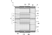
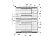
- FIG. 3 is a schematic cross-sectional view of a multilayer inductor element.
- FIG. 3 is a stacking diagram illustrating layers before firing of the multilayer inductor element illustrated in FIG. 2.
- FIG. 6 is a schematic cross-sectional view of another example of a multilayer inductor element.
- FIG. 2 is a schematic cross-sectional view of a multilayer inductor element.
- FIG. 3 is a stack diagram showing each layer before firing of the multilayer inductor element shown in FIG.
- the multilayer inductor element according to the present embodiment is used in, for example, a non-insulated DC-DC converter mounted on a mobile phone or the like.
- the multilayer inductor element 1 includes a multilayer substrate 2 and an inductor 3.
- the laminated substrate 2 has a configuration in which a total of 16 magnetic layers 4 and nonmagnetic layers 5 are laminated.
- the first layer, the eighth layer, and the sixteenth layer counted from the upper surface of the multilayer substrate 2 are the nonmagnetic layer 5, and the other layers are the magnetic layer 4.
- the parentheses shown in FIG. 3 indicate the number of each layer. For example, in the case of the first layer, (1) is set.
- the magnetic layer 4 is composed mainly of magnetic ferrite and a ceramic material.
- the magnetic layer 4 preferably has a thickness after firing of about 100 to 2000 ⁇ m and a magnetic permeability of about 290.
- the nonmagnetic layer 5 is mainly composed of a nonmagnetic ferrite and a ceramic material.
- the nonmagnetic layer 5 preferably has a thickness after firing of about 10 to 100 ⁇ m and a permeability of about 1.
- the nonmagnetic material layer 5 serving as the outermost layer (first layer and 16th layer) is made of LTCC (low temperature co-fired ceramics) and has a cover layer 6 having a thickness after firing of about 10 to 400 ⁇ m.
- the LTCC forming the cover layer 6 can be fired at a “low temperature” of about 900 ° C. or less. Accordingly, the multilayer inductor element 1 in which a coil conductor or the like described later using Cu or Ag having a low melting point is formed can be integrated by firing the cover layer 6 at the same time.
- the cover layer 6 is provided with mounting lands 10A and 10B which are terminals for mounting electronic components to be mounted.
- the cover layer 6 prevents the solder from eroding the nonmagnetic material layer 5. it can. Thereby, it can prevent that the reliability of the multilayer inductor element 1 falls.
- the inductor 3 has a configuration in which a plurality of coil conductors 7 are spirally connected via via-hole conductors (not shown) with the substrate lamination direction of the multilayer substrate 2 as an axial direction.
- the coil conductor 7 is provided on the upper surface of each layer from the fifth layer to the twelfth layer excluding the seventh layer and the ninth layer of the multilayer substrate 2.
- One end of the inductor 3, specifically, one end of the coil conductor 7 provided on the upper surface of the fifth layer is connected to a conductor 9 ⁇ / b> A provided on the upper surface of the second layer of the multilayer substrate 2 via the via-hole conductor 8 ⁇ / b> A. ing.
- a mounting land 10A is provided on the upper surface of the first layer, and the conductor 9A and the mounting land 10A are electrically connected via a via-hole conductor 11A formed in the first layer.
- the other end of the inductor 3, specifically, one end of the coil conductor 7 provided on the upper surface of the twelfth layer is connected to the conductor 9B provided on the upper surface of the sixteenth layer of the multilayer substrate 2 via the via-hole conductor 8B. It is connected to the.
- a mounting land 10B is provided on the lower surface of the sixteenth layer, and the conductor 9B and the mounting land 10B are electrically connected via a via-hole conductor 11B formed in the sixteenth layer.
- via-hole conductors 8C and 8D for conducting the upper and lower coil conductors 7 are formed in the seventh and ninth magnetic layers 4 where the coil conductor 7 is not formed.
- a coil is connected between the mounting lands 10A and 10B, and one of the mounting lands 10A and 10B is an input terminal, and the other is an output terminal.
- a gap 12 is provided in the region from the fifth layer to the twelfth layer where the inductor 3 is formed, on the upper surface side of the seventh layer and on the upper surface side of the ninth layer.
- a burnt material paste 12A such as carbon or resin is applied to the upper surface side of the seventh layer and the upper surface side of the ninth layer, and the burnt material paste 12A is burned off when the multilayer substrate 2 is fired.
- the burnt-out material paste 12A is applied in a ring shape, so that the gap 12 is provided in the spirally formed inductor.
- the gap 12 is not provided, a compressive stress is applied to the laminated substrate 2 after firing due to the difference between the thermal expansion coefficient of the magnetic layer 4 and the thermal expansion coefficient of the nonmagnetic layer 5. The efficiency will be reduced. For this reason, by providing the gap portion 12, the stress in the peripheral portion of the coil conductor 7 can be relaxed, and the coil characteristics such as the improvement of the voltage conversion rate or the improvement of the inductance value due to the iron loss suppression can be improved. it can.
- each inductor is provided as an inductor having a magnetic gap by inserting two nonmagnetic layers 5 in the middle (eighth layer) of the region from the fifth layer to the twelfth layer where the inductor 3 is formed. 3 is constituted.
- the non-magnetic layer 5 is configured such that both surfaces of the non-magnetic layer 5 are sandwiched between the coil conductors 7, thereby improving the DC superposition characteristics.
- the difference between the thermal expansion coefficient of the magnetic layer 4 and the thermal expansion coefficient of the nonmagnetic layer 5 is greater than 0 and less than 1 ppm / ° C. Is preferred.
- any method can be used for manufacturing the multilayer inductor element 1 as long as it is a manufacturing method in which unfired ceramic green sheets are stacked and fired. Therefore, for example, the multilayer inductor element 1 can be manufactured by a non-shrinkage method.
- the non-shrinkage construction method consists of an unfired multilayer ceramic body made by laminating a ceramic green sheet that can be fired at a low temperature and a conductor pattern made of a low melting point metal, and a constraining layer material made of alumina, etc.
- the constraining layer material is removed after firing at about 850 to 990 ° C. with a thickness of 1000 ⁇ m. According to this method, warping and distortion of the substrate can be suppressed.
- FIG. 4 is a schematic cross-sectional view of another example of the multilayer inductor element 1.
- the mounting lands 10 ⁇ / b> A and 10 ⁇ / b> B are directly provided on the surface of the nonmagnetic material layer 5, and are made of LTCC only around the mounting lands 10 ⁇ / b> A and 10 ⁇ / b> B, that is, only in the exposed portions of the nonmagnetic material layer 5.
- a cover layer 6 may be provided.
Landscapes
- Engineering & Computer Science (AREA)
- Power Engineering (AREA)
- Microelectronics & Electronic Packaging (AREA)
- Coils Or Transformers For Communication (AREA)
Abstract
表面に部品を実装した場合に信頼性が低減する可能性を抑制することができる積層型インダクタ素子を提供する。 磁性体層(4)を含む複数層が積層されてなる積層基板(2)と、積層基板(2)の層間に設けられたコイル導体(7)を、積層基板(2)の積層方向に接続したインダクタ(3)と、積層方向において積層基板(2)を挟み込むように、積層基板(2)に積層された一対の非磁性体層(5)と、を備え、非磁性体層(5)は低温同時焼成セラミックのカバー層(6)を有している。
Description
本発明は、磁性体層を備える積層基板にコイル導体を設けてインダクタを構成した積層型インダクタ素子に関する。
近年、電子部品の小型化又は薄型化が進んでいる。例えば、ガラスセラミックスからなる絶縁層が積層されたセラミック基板の内部にコイル導体を形成した積層型セラミック電子部品がある(例えば、特許文献1参照)。図1は特許文献1に記載の積層型セラミック電子部品の断面図である。
特許文献1に記載の積層型セラミック電子部品は、セラミック積層体101を備えている。セラミック積層体101は、内部または外部にコイルを構成する導体パターンが形成されたセラミック基材層102と、セラミック基材層102の上下主面に積層されたセラミック補助層103,104とを有している。セラミック積層体101は、内部または外部に導体パターンを形成している。セラミック積層体101の表面には、表面実装部品109,110などのIC(Integrated Circuit)が搭載され、内部には導体パターン106,107が形成される。
高いインダクタンス値を得るためには、セラミック基材層102は磁性体フェライトであることが望ましく、セラミック補助層103,104は、磁性体フェライトからなるセラミック基材層102との収縮差等による焼成時の構造欠陥を防ぐために、低透磁率または非磁性のフェライト(例えば,Fe,Zn,Cu)であることが望ましい。導体パターン106,107に電流が流れることにより、不要な磁場が発生し、例えば、表面実装部品109,110やセラミック基材層102に内蔵されたコイルパターン108の電気的特性に影響を及ぼすことがあるが、セラミック補助層103,104が、低透磁率または非磁性のフェライトとすることで、導体パターン106,107からの不要な磁場の発生を抑制することができる。
フェライト材料は有機酸に弱いことが一般的に知られているが、特許文献1では、表面実装部品109,110等を半田によりセラミック補助層103に実装している。このため、セラミック補助層103を非磁性フェライトで形成した場合、半田に含まれるフラックスやメッキ処理等によりフェライト材料に悪影響を及ぼすことが想定され、電子機器の組み立て工程等で電子部品に対してどのような処理がなされるか分からないため、何らかのコーティング処理がなされていることが望ましい。
そこで、本発明の目的は、表面に部品を実装した場合に信頼性が低減する可能性を抑制することができる積層型インダクタ素子を提供することにある。
本発明に係る積層型インダクタ素子は、磁性体層を含む複数層が積層されてなる積層基板と、該積層基板の層間に設けられたコイル導体を、前記積層基板の積層方向に接続したインダクタと、前記積層方向において前記積層基板を挟み込むように、前記積層基板に積層された一対の非磁性体層と、を備え、前記非磁性体層は低温同時焼成セラミックを有している。
この構成では、最外層である非磁性体層が低温同時焼成セラミックを有するため、非磁性体層に電子部品を実装する際の半田付けやメッキ等の処理に対する耐環境性を確保することができると共に、表面に部品を実装しても信頼性を損なうことを防止できる。また、非磁性体層が低温同時焼成セラミックを有するため、積層した磁性体層を焼成する際に同時焼成が可能となり、積層型インダクタ素子の生産性を高めることができる。
なお、非磁性体層は、表面の一部の必要箇所にのみ低温同時焼成セラミックが設けられて(塗布されて)いてもよいし、表面全体に設けられていてもよい。また、非磁性体層の主成分を低温同時焼成セラミックとしてもよい。
本発明に係る積層型インダクタ素子において、前記非磁性体層は、表面に形成された導体パターンと、該導体パターンおよび前記コイル導体を電気的に接続するビア導体と、を有することが好ましい。
この構成では、表面に形成した導体パターンと、磁性体層のコイル導体とを導通させることができ、配線構造を単純にできる。
本発明に係る積層型インダクタ素子において、前記積層基板は前記コイル導体の周囲に空隙を形成している構成でもよい。
この構成では、コイル導体の間に空隙が設けられるため、軽負荷領域での積層型インダクタ素子におけるインダクタンス値を大きくすることができ、さらに、重負荷領域での直流重畳特性を維持させることができる。
本発明に係る積層型インダクタ素子において、前記磁性体層の熱膨張係数と前記非磁性体層の熱膨張係数との差分は、0ppm/℃より大きく、1ppm/℃未満である構成が好ましい。
この構成では、磁性体層および非磁性体層の熱膨張係数の差を小さくすることで、焼成時に、インダクタンス値を大きくするために設けた空隙にクラックが入ることを防止することができる。
本発明によれば、積層型インダクタ素子の表面に部品を実装しても信頼性を損なうことを防止でき、また、積層型インダクタ素子の生産性を高めることができる。
図2は積層型インダクタ素子の模式断面図である。図3は図2に示す積層型インダクタ素子の焼成前の各層を示す積み図である。本実施形態に係る積層型インダクタ素子は、例えば、携帯電話機等に搭載される非絶縁型DC-DCコンバータに用いられる。
積層型インダクタ素子1は、積層基板2とインダクタ3とを備える。積層基板2は、合わせて16層の磁性体層4と非磁性体層5とを積層した構成である。積層基板2の上面から数えて第1層、第8層、第16層が非磁性体層5となっており、それ以外の層が磁性体層4となっている。なお、図3に示す括弧書きは各層の番号を示している。例えば第1層の場合は(1)とする。
磁性体層4は、磁性を有するフェライトとセラミック材料とを主成分とするものである。磁性体層4は、焼成後の厚みが100~2000μm程度であり、透磁率が290程度であることが好ましい。
非磁性体層5は、非磁性なフェライトとセラミック材料とを主成分とするものである。非磁性体層5は、焼成後の厚みが10~100μm程度であり、透磁率が1程度であることが好ましい。最外層(第1層および第16層)となる非磁性体層5は、LTCC(低温同時焼成セラミックス)からなり、焼成後の厚みが10~400μm程度のカバー層6を有している。
カバー層6を形成するLTCCは、約900℃程度以下の「低温」で焼成することが可能である。従って、これにより融点の低いCuやAgを使った後述のコイル導体等を内部に作りこんだ積層型インダクタ素子1は、カバー層6を同時に焼成して一体化することが可能となる。
このカバー層6には、実装する電子部品の実装用端子となる実装ランド10A,10Bが設けられている。非磁性体層5の表面にLTCCのカバー層6を設けることで、実装ランド10A,10Bに電子部品を半田により実装する場合、カバー層6により半田が非磁性体層5に浸食することを防止できる。これにより、積層型インダクタ素子1の信頼性が低下することを防止できる。
インダクタ3は、積層基板2の基板積層方向を軸方向として複数のコイル導体7を、ビアホール導体(不図示)を介して螺旋状に接続した構成である。コイル導体7は、積層基板2の第7層と第9層とを除く第5層から第12層までの各層上面に設けられる。
インダクタ3の一端部、具体的には、第5層上面に設けられたコイル導体7の一端部は、ビアホール導体8Aを介して積層基板2の第2層上面に設けられた導体9Aに接続されている。第1層上面には、実装ランド10Aが設けられており、第1層に形成されたビアホール導体11Aを介して導体9Aと実装ランド10Aとが導通している。
また、インダクタ3の他端部、具体的には、第12層上面に設けられたコイル導体7の一端部は、ビアホール導体8Bを介して積層基板2の第16層上面に設けられた導体9Bに接続されている。第16層下面には、実装ランド10Bが設けられており、第16層に形成されたビアホール導体11Bを介して導体9Bと実装ランド10Bとが導通している。
なお、コイル導体7が形成されていない第7層および第9層の磁性体層4には、上下層のコイル導体7を導通させるためのビアホール導体8C,8Dが形成されている。
すなわち、実装ランド10A,10Bの間にコイルが接続された構成となり、実装ランド10A,10Bの一方が入力端子となり、他方が出力端子となる。
積層基板2において、インダクタ3が形成される第5層から第12層までの領域内、第7層の上面側および第9層の上面側には空隙部12が設けられている。製造段階では、図3に示すように第7層の上面側および第9層の上面側にカーボンや樹脂等の焼失材ペースト12Aを塗布し、焼失材ペースト12Aを積層基板2の焼成時に焼失させて、空隙部12が形成される。焼失材ペースト12Aは環状に塗布していて、これにより螺旋状に形成されるインダクタ内に空隙部12が設けられるようにしている。
空隙部12を設けないと、磁性体層4の熱膨張係数と非磁性体層5の熱膨張係数との差により、焼成後の積層基板2内には圧縮応力がかかるため、鉄損によるコイルの効率低下が生じることとなる。このため、空隙部12を設けることで、コイル導体7の周辺部の応力を緩和させることができ、鉄損抑制による電圧の変換率向上、あるいはインダクタンス値の向上などのコイル特性を向上させることができる。
またここでは、インダクタ3が形成される第5層から第12層までの領域の中間(第8層)に非磁性体層5を2層挿入することで、磁気ギャップを備えたインダクタとして各インダクタ3を構成している。インダクタ3に磁気ギャップを設けることによってインダクタンス値を向上させることができる。そして、それらの非磁性体層5の両面がコイル導体7で挟まれるように構成して、このことにより直流重畳特性を改善するようにしている。
また、空隙部12を設ける場合、積層型インダクタ素子1において、磁性体層4の熱膨張係数と非磁性体層5の熱膨張係数との差分は、0より大きく、1ppm/℃未満であることが好ましい。熱膨張係数の差を小さくすることで、焼成時に、インダクタンス値を大きくするために設けた空隙部12を起点とするクラックの抑制を図ることができる。
なお、積層型インダクタ素子1の製造には、未焼成のセラミックグリーンシートを積層して焼成する製法であればどのような製法を用いてもよい。そのため、例えば無収縮工法によって積層型インダクタ素子1を製造することもできる。
無収縮工法は、低温焼成可能なセラミックグリーンシートと低融点金属による導体パターンとを積層してなる未焼成の多層セラミック体を構成し、その上下両主面にアルミナ等による拘束層材料を50~1000μm挟み、850~990℃程度で焼成させた後、拘束層材料を除去するという工法である。この工法によれば、基板の反りや歪みを抑制することができる。
なお、図2では、非磁性体層5の表面一面にカバー層6を設けているが、実装ランド9A,9B以外の部分にカバー層を設けてもよい。図4は積層型インダクタ素子1の他の例の模式断面図である。図4に示すように、実装ランド10A,10Bは非磁性体層5の表面に直接設け、実装ランド10A,10Bの周囲、すなわち、非磁性体層5が露出している部分にのみLTCCからなるカバー層6を設けるようにしてもよい。
なお、積層型インダクタ素子1の具体的構成などは、適宜設計変更可能であり、上述の実施形態に記載された作用及び効果は、本発明から生じる最も好適な作用及び効果を列挙したに過ぎず、本発明による作用及び効果は、上述の実施形態に記載されたものに限定されるものではない。
1-積層型インダクタ素子
2-積層基板
3-インダクタ
4-磁性体層
5-非磁性体層
6-カバー層(低温同時焼成セラミック)
7-コイル導体
10A,10B-実装ランド(導体パターン)
11A,11B-ビアホール導体(ビア導体)
12-空隙部
2-積層基板
3-インダクタ
4-磁性体層
5-非磁性体層
6-カバー層(低温同時焼成セラミック)
7-コイル導体
10A,10B-実装ランド(導体パターン)
11A,11B-ビアホール導体(ビア導体)
12-空隙部
Claims (4)
- 磁性体層を含む複数層が積層されてなる積層基板と、
該積層基板の層間に設けられたコイル導体を、前記積層基板の積層方向に接続したインダクタと、
前記積層方向において前記積層基板を挟み込むように、前記積層基板に積層された一対の非磁性体層と、
を備え、
前記非磁性体層は低温同時焼成セラミックを有している、積層型インダクタ素子。 - 前記非磁性体層は、
表面に形成された導体パターンと、
該導体パターンおよび前記コイル導体を電気的に接続するビア導体と、
を有する請求項1に記載の積層型インダクタ素子。 - 前記積層基板は前記コイル導体の周囲に空隙を形成している、請求項1又は2に記載の積層型インダクタ素子。
- 前記磁性体層の熱膨張係数と前記非磁性体層の熱膨張係数との差分は、0ppm/℃より大きく、1ppm/℃未満である、請求項3に記載の積層型インダクタ素子。
Priority Applications (3)
| Application Number | Priority Date | Filing Date | Title |
|---|---|---|---|
| JP2012557784A JPWO2012111203A1 (ja) | 2011-02-15 | 2011-11-17 | 積層型インダクタ素子 |
| CN2011800591928A CN103262187A (zh) | 2011-02-15 | 2011-11-17 | 层叠型电感元件 |
| US13/947,225 US20130293216A1 (en) | 2011-02-15 | 2013-07-22 | Laminated inductor element |
Applications Claiming Priority (2)
| Application Number | Priority Date | Filing Date | Title |
|---|---|---|---|
| JP2011-029773 | 2011-02-15 | ||
| JP2011029773 | 2011-02-15 |
Related Child Applications (1)
| Application Number | Title | Priority Date | Filing Date |
|---|---|---|---|
| US13/947,225 Continuation US20130293216A1 (en) | 2011-02-15 | 2013-07-22 | Laminated inductor element |
Publications (1)
| Publication Number | Publication Date |
|---|---|
| WO2012111203A1 true WO2012111203A1 (ja) | 2012-08-23 |
Family
ID=46672153
Family Applications (1)
| Application Number | Title | Priority Date | Filing Date |
|---|---|---|---|
| PCT/JP2011/076478 WO2012111203A1 (ja) | 2011-02-15 | 2011-11-17 | 積層型インダクタ素子 |
Country Status (4)
| Country | Link |
|---|---|
| US (1) | US20130293216A1 (ja) |
| JP (1) | JPWO2012111203A1 (ja) |
| CN (1) | CN103262187A (ja) |
| WO (1) | WO2012111203A1 (ja) |
Cited By (4)
| Publication number | Priority date | Publication date | Assignee | Title |
|---|---|---|---|---|
| KR20150114746A (ko) * | 2014-04-02 | 2015-10-13 | 삼성전기주식회사 | 적층형 전자부품 및 그 제조 방법 |
| JP2016213332A (ja) * | 2015-05-11 | 2016-12-15 | パナソニックIpマネジメント株式会社 | コモンモードノイズフィルタ |
| JP2019016727A (ja) * | 2017-07-10 | 2019-01-31 | 株式会社村田製作所 | コイル部品 |
| JP2020072154A (ja) * | 2018-10-30 | 2020-05-07 | Tdk株式会社 | 積層コイル部品 |
Families Citing this family (7)
| Publication number | Priority date | Publication date | Assignee | Title |
|---|---|---|---|---|
| CN107025990B (zh) * | 2017-04-18 | 2018-12-25 | 上海激光电源设备有限责任公司 | 光纤激光电源用高功率密度变压器 |
| JP6642544B2 (ja) * | 2017-09-12 | 2020-02-05 | 株式会社村田製作所 | コイル部品 |
| JP7032214B2 (ja) | 2018-04-02 | 2022-03-08 | 株式会社村田製作所 | 積層型コイル部品 |
| JP6954217B2 (ja) * | 2018-04-02 | 2021-10-27 | 株式会社村田製作所 | 積層型コイル部品 |
| KR20200036237A (ko) * | 2018-09-28 | 2020-04-07 | 삼성전기주식회사 | 코일 전자 부품 |
| JP7092070B2 (ja) * | 2019-03-04 | 2022-06-28 | 株式会社村田製作所 | 積層型コイル部品 |
| JP7078016B2 (ja) * | 2019-06-17 | 2022-05-31 | 株式会社村田製作所 | インダクタ部品 |
Citations (5)
| Publication number | Priority date | Publication date | Assignee | Title |
|---|---|---|---|---|
| JPH0864421A (ja) * | 1994-08-19 | 1996-03-08 | Murata Mfg Co Ltd | 積層セラミック電子部品およびその製造方法 |
| JPH09283359A (ja) * | 1996-04-16 | 1997-10-31 | Matsushita Electric Ind Co Ltd | 電子部品およびその製造方法 |
| JP2006352018A (ja) * | 2005-06-20 | 2006-12-28 | Tdk Corp | 積層型電子部品 |
| JP2007266245A (ja) * | 2006-03-28 | 2007-10-11 | Kyocera Corp | コイル内蔵基板 |
| WO2007145189A1 (ja) * | 2006-06-14 | 2007-12-21 | Murata Manufacturing Co., Ltd. | 積層型セラミック電子部品 |
Family Cites Families (6)
| Publication number | Priority date | Publication date | Assignee | Title |
|---|---|---|---|---|
| US5349743A (en) * | 1991-05-02 | 1994-09-27 | At&T Bell Laboratories | Method of making a multilayer monolithic magnet component |
| US5312674A (en) * | 1992-07-31 | 1994-05-17 | Hughes Aircraft Company | Low-temperature-cofired-ceramic (LTCC) tape structures including cofired ferromagnetic elements, drop-in components and multi-layer transformer |
| KR100755088B1 (ko) * | 2003-03-28 | 2007-09-03 | 티디케이가부시기가이샤 | 다층 기판 및 그 제조방법 |
| US7417001B2 (en) * | 2004-03-01 | 2008-08-26 | Murata Manufacturing Co., Ltd | Glass ceramic composition, glass-ceramic sintered body, and monolithic ceramic electronic component |
| US7340825B2 (en) * | 2006-07-06 | 2008-03-11 | Harris Corporation | Method of making a transformer |
| DE102008046336A1 (de) * | 2008-09-09 | 2010-03-11 | Osram Gesellschaft mit beschränkter Haftung | LTCC-Schichtstapel |
-
2011
- 2011-11-17 WO PCT/JP2011/076478 patent/WO2012111203A1/ja active Application Filing
- 2011-11-17 CN CN2011800591928A patent/CN103262187A/zh active Pending
- 2011-11-17 JP JP2012557784A patent/JPWO2012111203A1/ja active Pending
-
2013
- 2013-07-22 US US13/947,225 patent/US20130293216A1/en not_active Abandoned
Patent Citations (5)
| Publication number | Priority date | Publication date | Assignee | Title |
|---|---|---|---|---|
| JPH0864421A (ja) * | 1994-08-19 | 1996-03-08 | Murata Mfg Co Ltd | 積層セラミック電子部品およびその製造方法 |
| JPH09283359A (ja) * | 1996-04-16 | 1997-10-31 | Matsushita Electric Ind Co Ltd | 電子部品およびその製造方法 |
| JP2006352018A (ja) * | 2005-06-20 | 2006-12-28 | Tdk Corp | 積層型電子部品 |
| JP2007266245A (ja) * | 2006-03-28 | 2007-10-11 | Kyocera Corp | コイル内蔵基板 |
| WO2007145189A1 (ja) * | 2006-06-14 | 2007-12-21 | Murata Manufacturing Co., Ltd. | 積層型セラミック電子部品 |
Cited By (8)
| Publication number | Priority date | Publication date | Assignee | Title |
|---|---|---|---|---|
| KR20150114746A (ko) * | 2014-04-02 | 2015-10-13 | 삼성전기주식회사 | 적층형 전자부품 및 그 제조 방법 |
| JP2015198240A (ja) * | 2014-04-02 | 2015-11-09 | サムソン エレクトロ−メカニックス カンパニーリミテッド. | 積層型電子部品及びその製造方法 |
| KR101994734B1 (ko) * | 2014-04-02 | 2019-07-01 | 삼성전기주식회사 | 적층형 전자부품 및 그 제조 방법 |
| JP2016213332A (ja) * | 2015-05-11 | 2016-12-15 | パナソニックIpマネジメント株式会社 | コモンモードノイズフィルタ |
| JP2019016727A (ja) * | 2017-07-10 | 2019-01-31 | 株式会社村田製作所 | コイル部品 |
| US10872718B2 (en) | 2017-07-10 | 2020-12-22 | Murata Manufacturing Co., Ltd. | Coil component |
| JP2020072154A (ja) * | 2018-10-30 | 2020-05-07 | Tdk株式会社 | 積層コイル部品 |
| JP7222217B2 (ja) | 2018-10-30 | 2023-02-15 | Tdk株式会社 | 積層コイル部品 |
Also Published As
| Publication number | Publication date |
|---|---|
| US20130293216A1 (en) | 2013-11-07 |
| JPWO2012111203A1 (ja) | 2014-07-03 |
| CN103262187A (zh) | 2013-08-21 |
Similar Documents
| Publication | Publication Date | Title |
|---|---|---|
| WO2012111203A1 (ja) | 積層型インダクタ素子 | |
| KR101670184B1 (ko) | 적층 전자부품 및 그 제조방법 | |
| US9251943B2 (en) | Multilayer type inductor and method of manufacturing the same | |
| JP4840447B2 (ja) | 積層型セラミック電子部品 | |
| KR102105389B1 (ko) | 적층 전자부품 | |
| KR102025708B1 (ko) | 칩 전자부품 및 그 실장기판 | |
| KR101994722B1 (ko) | 적층형 전자부품 | |
| JP3621300B2 (ja) | 電源回路用積層インダクタ | |
| JP5621573B2 (ja) | コイル内蔵基板 | |
| US8779884B2 (en) | Multilayered inductor and method of manufacturing the same | |
| JP2001044037A (ja) | 積層インダクタ | |
| JP6344521B2 (ja) | 積層コイル部品及びその製造方法、並びに、当該積層コイル部品を備えるdc−dcコンバータモジュール | |
| JP2007503716A (ja) | 極薄フレキシブル・インダクタ | |
| US8736413B2 (en) | Laminated type inductor element and manufacturing method therefor | |
| JP4213679B2 (ja) | 積層型インダクタ | |
| WO2012144103A1 (ja) | 積層型インダクタ素子及び製造方法 | |
| WO2011148678A1 (ja) | Lc共焼結基板及びその製造方法 | |
| JP2010245088A (ja) | 積層型セラミック電子部品の製造方法 | |
| KR20110132576A (ko) | 다층 회로 캐리어 및 그의 제조 방법 | |
| JPH06176928A (ja) | 積層電子部品 | |
| JP2016051752A (ja) | 積層型電子部品 | |
| JP2012138496A (ja) | コイル内蔵基板 | |
| JP2003017325A (ja) | 積層型金属磁性電子部品及びその製造方法 | |
| JP5617614B2 (ja) | コイル内蔵基板 | |
| JP6269541B2 (ja) | Dc−dcコンバータモジュールおよび製造方法 |
Legal Events
| Date | Code | Title | Description |
|---|---|---|---|
| 121 | Ep: the epo has been informed by wipo that ep was designated in this application |
Ref document number: 11859006 Country of ref document: EP Kind code of ref document: A1 |
|
| ENP | Entry into the national phase |
Ref document number: 2012557784 Country of ref document: JP Kind code of ref document: A |
|
| NENP | Non-entry into the national phase |
Ref country code: DE |
|
| 122 | Ep: pct application non-entry in european phase |
Ref document number: 11859006 Country of ref document: EP Kind code of ref document: A1 |