WO2012011446A1 - レーザ加工方法 - Google Patents
レーザ加工方法 Download PDFInfo
- Publication number
- WO2012011446A1 WO2012011446A1 PCT/JP2011/066242 JP2011066242W WO2012011446A1 WO 2012011446 A1 WO2012011446 A1 WO 2012011446A1 JP 2011066242 W JP2011066242 W JP 2011066242W WO 2012011446 A1 WO2012011446 A1 WO 2012011446A1
- Authority
- WO
- WIPO (PCT)
- Prior art keywords
- cutting line
- along
- modified region
- workpiece
- modified
- Prior art date
- Legal status (The legal status is an assumption and is not a legal conclusion. Google has not performed a legal analysis and makes no representation as to the accuracy of the status listed.)
- Ceased
Links
Images




Classifications
-
- B—PERFORMING OPERATIONS; TRANSPORTING
- B28—WORKING CEMENT, CLAY, OR STONE
- B28D—WORKING STONE OR STONE-LIKE MATERIALS
- B28D5/00—Fine working of gems, jewels, crystals, e.g. of semiconductor material; apparatus or devices therefor
- B28D5/0005—Fine working of gems, jewels, crystals, e.g. of semiconductor material; apparatus or devices therefor by breaking, e.g. dicing
- B28D5/0011—Fine working of gems, jewels, crystals, e.g. of semiconductor material; apparatus or devices therefor by breaking, e.g. dicing with preliminary treatment, e.g. weakening by scoring
-
- B—PERFORMING OPERATIONS; TRANSPORTING
- B23—MACHINE TOOLS; METAL-WORKING NOT OTHERWISE PROVIDED FOR
- B23K—SOLDERING OR UNSOLDERING; WELDING; CLADDING OR PLATING BY SOLDERING OR WELDING; CUTTING BY APPLYING HEAT LOCALLY, e.g. FLAME CUTTING; WORKING BY LASER BEAM
- B23K26/00—Working by laser beam, e.g. welding, cutting or boring
- B23K26/0006—Working by laser beam, e.g. welding, cutting or boring taking account of the properties of the material involved
-
- B—PERFORMING OPERATIONS; TRANSPORTING
- B23—MACHINE TOOLS; METAL-WORKING NOT OTHERWISE PROVIDED FOR
- B23K—SOLDERING OR UNSOLDERING; WELDING; CLADDING OR PLATING BY SOLDERING OR WELDING; CUTTING BY APPLYING HEAT LOCALLY, e.g. FLAME CUTTING; WORKING BY LASER BEAM
- B23K26/00—Working by laser beam, e.g. welding, cutting or boring
- B23K26/352—Working by laser beam, e.g. welding, cutting or boring for surface treatment
- B23K26/359—Working by laser beam, e.g. welding, cutting or boring for surface treatment by providing a line or line pattern, e.g. a dotted break initiation line
-
- B—PERFORMING OPERATIONS; TRANSPORTING
- B23—MACHINE TOOLS; METAL-WORKING NOT OTHERWISE PROVIDED FOR
- B23K—SOLDERING OR UNSOLDERING; WELDING; CLADDING OR PLATING BY SOLDERING OR WELDING; CUTTING BY APPLYING HEAT LOCALLY, e.g. FLAME CUTTING; WORKING BY LASER BEAM
- B23K2103/00—Materials to be soldered, welded or cut
- B23K2103/50—Inorganic materials other than metals or composite materials
- B23K2103/56—Inorganic materials other than metals or composite materials being semiconducting
Definitions
- the present invention relates to a laser processing method for cutting out a plurality of effective portions from a plate-like processing object.
- a modified region is formed inside the wafer along a planned cutting line by irradiating the wafer with laser light, and cracks generated from the modified region are removed from the front and back surfaces of the wafer. It is known that a plurality of chips are obtained by cutting the wafer along a planned cutting line (see, for example, Patent Document 1).
- the second scheduled cutting line along the outer edge of the second effective portion is directed toward the first effective portion.
- a state of hitting the first scheduled cutting line along the outer edge of the effective portion may occur. In such a state, when the modified region is formed along the second scheduled cutting line, a crack generated from the modified region reaches the first effective portion, and the first effective portion is damaged. May occur.
- an object of the present invention is to provide a laser processing method capable of forming a modified region along each scheduled cutting line while preventing damage to the first effective portion.
- a laser processing method is a laser processing method for cutting out at least a first effective portion and a second effective portion from a plate-like workpiece, and is along the outer edge of the first effective portion.
- a first modified region is formed inside the object to be processed along the first scheduled cutting line by relatively moving the condensing point of the laser light along the first scheduled cutting line.
- Laser beam along the outer edge of the second effective portion and the second planned cutting line that strikes the first planned cutting line toward the first effective portion after the first step and the first step A second step of forming a second modified region inside the workpiece along the second scheduled cutting line by relatively moving the condensing point.
- a first modified region is formed along a first scheduled cutting line, and then a second modified region is formed along a second scheduled cutting line. Therefore, with the formation of the second modified region, a crack is generated from the second modified region, and even if the crack is likely to extend toward the first effective portion, the extension of the crack is It is received by at least one of the first modified region and the crack generated from the first modified region. Therefore, according to this laser processing method, the second scheduled cutting line along the outer edge of the second effective portion is directed to the first effective portion along the outer edge of the first effective portion toward the first effective portion. In the case of hitting the line, it is possible to form the modified region along each scheduled cutting line while preventing the first effective portion from being damaged.
- the second modified region may be formed in a part of the second scheduled cutting line excluding a part of a predetermined distance from the first scheduled cutting line. According to this, the modified region is not formed in a portion of the second scheduled cutting line at a predetermined distance from the first scheduled cutting line. Accordingly, the formation of the second modified region prevents the second modified region from generating a crack in the vicinity of the first scheduled cutting line, and the crack generated from the second modified region is prevented. The extension toward the first effective portion can be suppressed.
- the modified regions closest to the laser light incident surface may be formed as the first modified region and the second modified region.
- the generation of cracks accompanying the formation of the modified region is more likely to occur in the modified region closer to the laser light incident surface than the modified region far from the laser light incident surface. Therefore, if at least the modified regions closest to the laser light incident surface are formed as the first modified region and the second modified region described above, it is possible to prevent the first effective portion from being damaged. it can.
- the cracks generated from the first modified region and the second modified region reach the front surface and the back surface of the workpiece, so that the first scheduled cutting line and the second modified line You may further provide the 3rd process of cut
- the second scheduled cutting line along the outer edge of the second effective portion hits the first planned cutting line along the outer edge of the first effective portion toward the first effective portion.
- the modified region can be formed along each scheduled cutting line while preventing the first effective portion from being damaged.
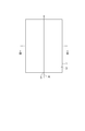
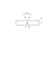
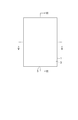
- FIG. 3 is a cross-sectional view taken along the line III-III of the workpiece in FIG. 2. It is a top view of the processing target after laser processing.
- FIG. 5 is a cross-sectional view taken along the line VV of the workpiece in FIG. 4.
- FIG. 5 is a cross-sectional view taken along line VI-VI of the workpiece in FIG. 4.
- the modified region is formed inside the processing object along the planned cutting line by irradiating the processing target with laser light along the planned cutting line.
- a laser processing apparatus 100 includes a laser light source 101 that oscillates a laser beam L, a dichroic mirror 103 that is arranged so as to change the direction of the optical axis (optical path) of the laser beam L, and A condensing lens 105 for condensing the laser light L. Further, the laser processing apparatus 100 includes a support base 107 for supporting the workpiece 1 irradiated with the laser light L condensed by the condensing lens 105, and a stage 111 for moving the support base 107. And a laser light source control unit 102 for controlling the laser light source 101 to adjust the output of the laser light L, the pulse width, and the like, and a stage control unit 115 for controlling the movement of the stage 111.
- the laser light L emitted from the laser light source 101 has its optical axis changed by 90 ° by the dichroic mirror 103, and the inside of the processing object 1 placed on the support base 107.
- the light is condensed by the condensing lens 105.
- the stage 111 is moved, and the workpiece 1 is moved relative to the laser beam L along the planned cutting line 5. As a result, a modified region along the planned cutting line 5 is formed on the workpiece 1.
- a scheduled cutting line 5 for cutting the workpiece 1 is set in the workpiece 1.
- the planned cutting line 5 is a virtual line extending linearly.
- the laser beam L is projected along the planned cutting line 5 in a state where the focused point P is aligned with the inside of the workpiece 1. It moves relatively (that is, in the direction of arrow A in FIG. 2).
- the modified region 7 is formed inside the workpiece 1 along the planned cutting line 5, and the modified region 7 formed along the planned cutting line 5 is formed. It becomes the cutting start area 8.
- the condensing point P is a location where the laser light L is condensed.
- the planned cutting line 5 is not limited to a straight line, but may be a curved line, or may be a line actually drawn on the surface 3 of the workpiece 1 without being limited to a virtual line.
- the modified region 7 may be formed continuously or intermittently. Further, the modified region 7 may be in the form of a line or a dot. In short, the modified region 7 only needs to be formed at least inside the workpiece 1.
- a crack may be formed starting from the modified region 7, and the crack and modified region 7 may be exposed on the outer surface (front surface, back surface, or outer peripheral surface) of the workpiece 1.
- the laser light L here passes through the workpiece 1 and is particularly absorbed near the condensing point inside the workpiece 1, thereby forming the modified region 7 in the workpiece 1. (Ie, internal absorption laser processing). Therefore, since the laser beam L is hardly absorbed by the surface 3 of the workpiece 1, the surface 3 of the workpiece 1 is not melted. In general, when a removed portion such as a hole or a groove is formed by being melted and removed from the front surface 3 (surface absorption laser processing), the processing region gradually proceeds from the front surface 3 side to the back surface side.
- the modified region formed in the present embodiment refers to a region in which density, refractive index, mechanical strength, and other physical characteristics are different from the surroundings.
- the modified region include a melt treatment region, a crack region, a dielectric breakdown region, a refractive index change region, and the like, and there is a region where these are mixed.
- the modified region there are a region in which the density of the modified region in the material to be processed is changed as compared with the density of the non-modified region, and a region in which lattice defects are formed (collectively these are high-density regions). Also known as the metastatic region).
- the area where the density of the melt-processed area, the refractive index changing area, the modified area is changed compared to the density of the non-modified area, or the area where lattice defects are formed is In some cases, cracks (cracks, microcracks) are included in the interface between the non-modified region and the non-modified region. The included crack may be formed over the entire surface of the modified region, or may be formed in only a part or a plurality of parts.
- the processing object 1 include those containing or consisting of silicon, glass, LiTaO 3 or sapphire (Al 2 O 3 ).
- the modified region 7 is formed by forming a plurality of modified spots (processing marks) along the planned cutting line 5.
- the modified spot is a modified portion formed by one pulse shot of pulsed laser light (that is, one pulse of laser irradiation: laser shot).
- Examples of the modified spot include a crack spot, a melting treatment spot, a refractive index change spot, or a mixture of at least one of these.
- the size of the modified spot and the length of the crack to be generated are appropriately determined. It is preferable to control.
- FIG. 7 is a plan view of a workpiece to be processed by the laser processing method according to the embodiment of the present invention.
- the workpiece 1 includes a silicon wafer 11 and a functional element layer 16 formed on the silicon wafer 11 including a plurality of functional elements 15.
- the workpiece 1 is a plate-like object having the surface on the functional element layer 16 side as the front surface 3 and the surface on the opposite side to the functional element layer 16 as the back surface 4.
- the functional element 15 is, for example, a semiconductor operation layer formed by crystal growth, a light receiving element such as a photodiode, a light emitting element such as a laser diode, or a circuit element formed as a circuit.
- the functional element 15 is formed for each rectangular effective portion 18.
- Each effective part 18 corresponds to a semiconductor chip acquired by cutting the workpiece 1.
- the effective portion 18 is arranged such that the direction parallel to the orientation flat 6 of the silicon wafer 11 is the long side direction (that is, the direction perpendicular to the orientation flat 6 is the short side direction). Further, the effective portions 18 are arranged in a line in the row direction (direction parallel to the orientation flat 6), while being arranged in a zigzag shape in the column direction (direction perpendicular to the orientation flat 6). This is to increase the number of semiconductor chips acquired from one silicon wafer 11.
- the planned cutting line 52 along the short side of one effective portion 18 is directed to the long side of the other effective portion 18 toward the other effective portion 18. It hits the middle part of the scheduled cutting line 51 along.
- a portion where the effective portion 18 cannot be disposed on the outer edge portion of the workpiece 1 is a non-effective portion 19.
- a plurality of effective portions 18 are cut out from the workpiece 1 as described above as follows. First, an expand tape is affixed on the back surface 4 of the workpiece 1, and the workpiece 1 is placed on the support 107 of the laser processing apparatus 100. Then, the stage 111 is controlled so that the condensing point P of the laser light L is located inward from the surface 3 of the workpiece 1 by a predetermined distance.
- the processing object 1 is irradiated with the laser light L along the scheduled cutting line 51 with the surface 3 of the processing object 1 as the laser light incident surface. That is, the condensing point P of the laser light L is relatively moved (scanned) along the planned cutting line 51 along the long side of the effective portion 18.
- the stage 111 is controlled to scan the laser light L.
- a modified region 71 is formed inside the workpiece 1 along the planned cutting line 51 as shown in FIG.
- the processing target 1 is irradiated with the laser beam L along the planned cutting line 52 using the surface 3 of the processing target 1 as the laser light incident surface. That is, the condensing point P of the laser light L is relatively moved along the planned cutting line 52 along the short side of the effective portion 18.
- a modified region 72 is formed inside the workpiece 1 along the planned cutting line 52 as shown in FIG.
- the modified region 72 is formed in the intermediate portion 52b of the planned cutting line 52 excluding the end portion 52a at a predetermined distance from the planned cutting line 51.
- the length of the end portion 52a corresponding to the predetermined distance is such that a crack generated from the modified region 72 is scheduled to be cut along with the formation of the modified region 72 (that is, substantially simultaneously with the formation of the modified region 72). It is preferable that the distance extends in the direction of 52, for example, about 10 ⁇ m.
- the modified region 72 is not formed with the modified region 72 but the modified region 72 is not provided. Cross.
- the expanded tape attached to the back surface 4 of the workpiece 1 is expanded, and cracks generated from the modified regions 71 and 72 are processed. 1, the workpiece 1 is cut along the scheduled cutting lines 51 and 52. As a result, as shown in FIG. 10, a plurality of effective portions 18 are cut out from the workpiece 1, and a plurality of semiconductor chips 25 having functional elements 15 are obtained.
- the planned cutting line 52 along the short side of one effective part 18 is directed toward the other effective part 18 at the intermediate portion of the planned cutting line 51 along the long side of the other effective part 18.
- the modified region 71 is formed along the planned cutting line 51 along the long side
- the modified region 72 is formed along the planned cutting line 52 along the short side.
- a crack 17 is generated from the modified region 72, and the crack 17 is likely to extend toward the other effective portion 18,
- the extension of the crack 17 is received by the modified region 71 that has already been formed and the crack 17 that has occurred from the modified region 71. Therefore, it is possible to form the modified regions 71 and 72 along the scheduled cutting lines 51 and 52 while preventing the effective portions 18 from being damaged.
- the crack 17 here is the thickness of the workpiece 1 from the modified regions 71 and 72 with the formation of the modified regions 71 and 72 (even if no external force is applied to the workpiece 1). It occurs in the direction and the direction of the scheduled cutting lines 51 and 52.
- the modified region 72 when the modified region 72 is formed along the planned cutting line 52 along the short side, the modified region 72 is formed in the intermediate portion 52 b of the planned cutting line 52, and the planned cutting line 52 is formed.
- the modified region 72 is not formed in the end portion 52a. This prevents the crack 17 from being generated from the modified region 72 in the vicinity of the planned cutting line 51 along the long side as the modified region 72 is formed. It is possible to suppress extension toward the effective portion 18 of the.
- the crack 17 generated from the modified regions 71 and 72 reaches the front surface 3 and the back surface 4 of the workpiece 1, the workpiece 1 is cut along the scheduled cutting lines 51 and 52.
- the part 18 can be accurately cut out from the workpiece 1.
- the corner of the effective portion 18 located at the boundary between the effective portion 18 and the non-effective portion 19 the modified region 71 and the modified region 72 intersect with each other. Damage can be prevented from occurring.
- FIG. 12 shows the processing target 1 after forming the modified regions 71 and 72 along the scheduled cutting lines 51 and 52 and before expanding the expanded tape attached to the back surface 4 of the processing target 1. It is a figure which shows a plane photograph. As shown in FIG. 12, in this case, the crack 17 generated from the modified regions 71 and 72 with the formation of the modified regions 71 and 72 has reached the surface 3 of the workpiece 1. The extension of the crack 17 along the line 52 was received by the modified region 71 and the crack 17 along the planned cutting line 51.
- FIG. 13 is a diagram showing a plane photograph of the processing object after the expanded tape attached to the back surface 4 of the processing object 1 in FIG. 12 is expanded. As shown in FIG. 13, it was possible to prevent the effective portions 18 from being damaged and to cut out the plurality of semiconductor chips 25 from the workpiece 1 with high accuracy.
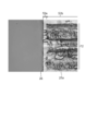
- FIG. 14 is a view showing a photograph of the cut surface 25 a of the semiconductor chip 25. As shown in FIG. 14, the modified region 72 is formed in the intermediate portion 52b of the planned cutting line 52 and the modified region 72 is not formed in the end portion 52a of the planned cutting line 52. Was cut along the scheduled cutting line 52 with high accuracy. In FIG. 12, the length of the end portion 52a where the modified region 72 is not formed is about 10 ⁇ m.
- the number of columns of the modified regions 71 and 72 formed for each of the scheduled cutting lines 51 and 52 is not limited to one column, and may be a plurality of columns.
- the number of rows can be appropriately determined according to the thickness of the workpiece 1 or the like.
- a plurality of rows of modified regions 71 may be formed along the planned cutting lines 51 along the lines, and then a plurality of rows of modified regions 72 may be formed along the planned cutting lines 52 along the short sides.
- the modified region 72 is formed along the planned cutting line 52 along the short side, the modified region 72 is formed in the intermediate portion 52b of the planned cutting line 52, and the end portion 52a of the planned cutting line 52 is The modified region 72 may not be formed.
- the modified regions 71 and 72 closest to the laser light incident surface (here, the surface 3) of the workpiece 1 are formed after the modified region 71 is formed, and further scheduled for cutting. If the modified region 72 is not formed in the end portion 52a of the line 52, the modified regions 71 and 72 are formed along the scheduled cutting lines 51 and 52 while preventing the effective portions 18 from being damaged. Sometimes you can. This is because the generation of the crack 17 accompanying the formation of the modified regions 71 and 72 is more likely to occur in the modified regions 71 and 72 closer to the laser light incident surface than the modified regions 71 and 72 far from the laser light incident surface. This is effective when the following formation order is taken.
- the modified regions 71 and 72 farthest from the laser light incident surface of the workpiece 1 are formed for all the scheduled cutting lines 51 and 52, and thereafter, every distance from the laser light incident surface of the workpiece 1.
- the modified regions 71 and 72 are formed for all the planned cutting lines 51 and 52.
- an external force is applied to the workpiece 1 by expanding the expanded tape to cause the cracks 17 to reach the front surface 3 and the back surface 4 of the workpiece 1, but the present invention is not limited to this.
- the front surface 3 and the back surface 4 of the workpiece 1 are cracked. In some cases, the workpiece 1 is cut along the scheduled cutting lines 51 and 52.
- the second scheduled cutting line along the outer edge of the second effective portion hits the first planned cutting line along the outer edge of the first effective portion toward the first effective portion.
- the modified region can be formed along each scheduled cutting line while preventing the first effective portion from being damaged.
Landscapes
- Engineering & Computer Science (AREA)
- Mechanical Engineering (AREA)
- Physics & Mathematics (AREA)
- Optics & Photonics (AREA)
- Plasma & Fusion (AREA)
- Dicing (AREA)
- Laser Beam Processing (AREA)
- Processing Of Stones Or Stones Resemblance Materials (AREA)
Abstract
板状の加工対象物から少なくとも第1の有効部及び第2の有効部を切り出すためのレーザ加工方法は、第1の有効部の外縁に沿う第1の切断予定ラインに沿って、レーザ光の集光点を相対的に移動させることにより、第1の切断予定ラインに沿って加工対象物の内部に第1の改質領域を形成する第1の工程と、第1の工程の後に、第2の有効部の外縁に沿いかつ第1の有効部に向かって第1の切断予定ラインに突き当たる第2の切断予定ラインに沿って、レーザ光の集光点を相対的に移動させることにより、第2の切断予定ラインに沿って加工対象物の内部に第2の改質領域を形成する第2の工程と、を備える。
Description
本発明は、板状の加工対象物から複数の有効部を切り出すためのレーザ加工方法に関する。
上記技術分野のレーザ加工方法として、ウェハにレーザ光を照射することにより、切断予定ラインに沿ってウェハの内部に改質領域を形成し、その改質領域から発生した亀裂をウェハの表面及び裏面に到達させることにより、切断予定ラインに沿ってウェハを切断し、複数のチップを取得するものが知られている(例えば、特許文献1参照)。
ところで、1枚のウェハからのチップの取得数を増加させる観点では、チップに対応する有効部をウェハに対してマトリックス状に配置するよりも、例えば列方向においてジグザグ状に配置するほうが有利な場合がある。また、例えば六角形等、四角形以外の有効部をウェハに対して複数設定すべき場合がある。これらの場合には、隣り合う第1の有効部及び第2の有効部において、第2の有効部の外縁に沿う第2の切断予定ラインが、第1の有効部に向かって、第1の有効部の外縁に沿う第1の切断予定ラインに突き当たる状態が生じ得る。このような状態においては、第2の切断予定ラインに沿って改質領域を形成した際に、その改質領域から発生した亀裂が第1の有効部内に至り、第1の有効部に損傷が生じるおそれがある。
そこで、本発明は、第2の有効部の外縁に沿う第2の切断予定ラインが、第1の有効部に向かって、第1の有効部の外縁に沿う第1の切断予定ラインに突き当たっている場合において、第1の有効部に損傷が生じるのを防止しつつ、各切断予定ラインに沿って改質領域を形成することができるレーザ加工方法を提供することを目的とする。
本発明の一側面のレーザ加工方法は、板状の加工対象物から少なくとも第1の有効部及び第2の有効部を切り出すためのレーザ加工方法であって、第1の有効部の外縁に沿う第1の切断予定ラインに沿って、レーザ光の集光点を相対的に移動させることにより、第1の切断予定ラインに沿って加工対象物の内部に第1の改質領域を形成する第1の工程と、第1の工程の後に、第2の有効部の外縁に沿いかつ第1の有効部に向かって第1の切断予定ラインに突き当たる第2の切断予定ラインに沿って、レーザ光の集光点を相対的に移動させることにより、第2の切断予定ラインに沿って加工対象物の内部に第2の改質領域を形成する第2の工程と、を備える。
このレーザ加工方法では、まず、第1の切断予定ラインに沿って第1の改質領域を形成し、その後に、第2の切断予定ラインに沿って第2の改質領域を形成する。そのため、第2の改質領域の形成に伴って、第2の改質領域から亀裂が発生し、その亀裂が第1の有効部に向かって伸展しそうになっても、その亀裂の伸展は、既に形成された第1の改質領域及び第1の改質領域から発生した亀裂の少なくとも一方によって受け止められる。よって、このレーザ加工方法によれば、第2の有効部の外縁に沿う第2の切断予定ラインが、第1の有効部に向かって、第1の有効部の外縁に沿う第1の切断予定ラインに突き当たっている場合において、第1の有効部に損傷が生じるのを防止しつつ、各切断予定ラインに沿って改質領域を形成することができる。
ここで、第2の工程においては、第2の切断予定ラインのうち第1の切断予定ラインから所定の距離の部分を除いた部分に、第2の改質領域を形成してもよい。これによれば、第2の切断予定ラインのうち第1の切断予定ラインから所定の距離の部分には改質領域が形成されない。従って、第2の改質領域の形成に伴って、第1の切断予定ラインの近傍で第2の改質領域から亀裂が発生するのを防止し、第2の改質領域から発生した亀裂が第1の有効部に向かって伸展するのを抑制することができる。
また、第1の切断予定ライン及び第2の切断予定ラインのそれぞれに対して、加工対象物の厚さ方向に並ぶように複数列の改質領域を形成する場合には、少なくとも加工対象物のレーザ光入射面に最も近い改質領域を第1の改質領域及び第2の改質領域として形成すればよい。改質領域の形成に伴う亀裂の発生は、レーザ光入射面から遠い改質領域よりもレーザ光入射面に近い改質領域で起こり易い。従って、少なくともレーザ光入射面に最も近い改質領域を、上述した第1の改質領域及び第2の改質領域として形成すれば、第1の有効部に損傷が生じるのを防止することができる。
また、第2の工程の後に、第1の改質領域及び第2の改質領域から発生した亀裂を加工対象物の表面及び裏面に到達させることにより、第1の切断予定ライン及び第2の切断予定ラインに沿って加工対象物を切断する第3の工程を更に備えてもよい。これによれば、第1の有効部及び第2の有効部を加工対象物から精度良く切り出すことができる。
本発明によれば、第2の有効部の外縁に沿う第2の切断予定ラインが、第1の有効部に向かって、第1の有効部の外縁に沿う第1の切断予定ラインに突き当たっている場合において、第1の有効部に損傷が生じるのを防止しつつ、各切断予定ラインに沿って改質領域を形成することができる。
以下、本発明の好適な実施形態について、図面を参照して詳細に説明する。なお、各図において同一又は相当部分には同一符号を付し、重複する説明を省略する。
本発明の一実施形態のレーザ加工方法では、切断予定ラインに沿って加工対象物にレーザ光を照射することにより、切断予定ラインに沿って加工対象物の内部に改質領域を形成する。そこで、まず、この改質領域の形成について、図1~図6を参照して説明する。
図1に示すように、レーザ加工装置100は、レーザ光Lをパルス発振するレーザ光源101と、レーザ光Lの光軸(光路)の向きを90°変えるように配置されたダイクロイックミラー103と、レーザ光Lを集光するための集光用レンズ105と、を備えている。また、レーザ加工装置100は、集光用レンズ105で集光されたレーザ光Lが照射される加工対象物1を支持するための支持台107と、支持台107を移動させるためのステージ111と、レーザ光Lの出力やパルス幅等を調節するためにレーザ光源101を制御するレーザ光源制御部102と、ステージ111の移動を制御するステージ制御部115と、を備えている。
このレーザ加工装置100においては、レーザ光源101から出射されたレーザ光Lは、ダイクロイックミラー103によってその光軸の向きを90°変えられ、支持台107上に載置された加工対象物1の内部に集光用レンズ105によって集光される。これと共に、ステージ111が移動させられ、加工対象物1がレーザ光Lに対して切断予定ライン5に沿って相対移動させられる。これにより、切断予定ライン5に沿った改質領域が加工対象物1に形成されることとなる。
加工対象物1としては、半導体材料や圧電材料等が用いられ、図2に示すように、加工対象物1には、加工対象物1を切断するための切断予定ライン5が設定されている。切断予定ライン5は、直線状に延びた仮想線である。加工対象物1の内部に改質領域を形成する場合、図3に示すように、加工対象物1の内部に集光点Pを合わせた状態で、レーザ光Lを切断予定ライン5に沿って(すなわち、図2の矢印A方向に)相対的に移動させる。これにより、図4~図6に示すように、改質領域7が切断予定ライン5に沿って加工対象物1の内部に形成され、切断予定ライン5に沿って形成された改質領域7が切断起点領域8となる。
なお、集光点Pとは、レーザ光Lが集光する箇所のことである。また、切断予定ライン5は、直線状に限らず曲線状であってもよいし、仮想線に限らず加工対象物1の表面3に実際に引かれた線であってもよい。また、改質領域7は、連続的に形成される場合もあるし、断続的に形成される場合もある。また、改質領域7は列状でも点状でもよく、要は、改質領域7は少なくとも加工対象物1の内部に形成されていればよい。また、改質領域7を起点に亀裂が形成される場合があり、亀裂及び改質領域7は、加工対象物1の外表面(表面、裏面、若しくは外周面)に露出していてもよい。
ちなみに、ここでのレーザ光Lは、加工対象物1を透過すると共に加工対象物1の内部の集光点近傍にて特に吸収され、これにより、加工対象物1に改質領域7が形成される(すなわち、内部吸収型レーザ加工)。よって、加工対象物1の表面3ではレーザ光Lが殆ど吸収されないので、加工対象物1の表面3が溶融することはない。一般的に、表面3から溶融され除去されて穴や溝等の除去部が形成される(表面吸収型レーザ加工)場合、加工領域は表面3側から徐々に裏面側に進行する。
ところで、本実施形態で形成される改質領域は、密度、屈折率、機械的強度やその他の物理的特性が周囲とは異なる状態になった領域をいう。改質領域としては、例えば、溶融処理領域、クラック領域、絶縁破壊領域、屈折率変化領域等があり、これらが混在した領域もある。更に、改質領域としては、加工対象物の材料において改質領域の密度が非改質領域の密度と比較して変化した領域や、格子欠陥が形成された領域がある(これらをまとめて高密転移領域ともいう)。
また、溶融処理領域や屈折率変化領域、改質領域の密度が非改質領域の密度と比較して変化した領域、格子欠陥が形成された領域は、更に、それら領域の内部や改質領域と非改質領域との界面に亀裂(割れ、マイクロクラック)を内包している場合がある。内包される亀裂は改質領域の全面に渡る場合や一部分のみや複数部分に形成される場合がある。加工対象物1としては、例えばシリコン、ガラス、LiTaO3又はサファイア(Al2O3)を含む、又はこれらからなるものが挙げられる。
また、本実施形態においては、切断予定ライン5に沿って改質スポット(加工痕)を複数形成することによって、改質領域7を形成している。改質スポットとは、パルスレーザ光の1パルスのショット(つまり1パルスのレーザ照射:レーザショット)で形成される改質部分であり、改質スポットが集まることにより改質領域7となる。改質スポットとしては、クラックスポット、溶融処理スポット若しくは屈折率変化スポット、又はこれらの少なくとも1つが混在するもの等が挙げられる。
この改質スポットについては、要求される切断精度、要求される切断面の平坦性、加工対象物の厚さ、種類、結晶方位等を考慮して、その大きさや発生する亀裂の長さを適宜制御することが好ましい。
次に、本発明の一実施形態のレーザ加工方法について詳細に説明する。図7は、本発明の一実施形態のレーザ加工方法の対象となる加工対象物の平面図である。図7に示すように、加工対象物1は、シリコンウェハ11と、複数の機能素子15を含んでシリコンウェハ11上に形成された機能素子層16と、を備えている。加工対象物1は、機能素子層16側の面を表面3とし、機能素子層16と反対側の面を裏面4とする板状のものである。機能素子15は、例えば、結晶成長により形成された半導体動作層、フォトダイオード等の受光素子、レーザダイオード等の発光素子、或いは回路として形成された回路素子等である。
機能素子15は、長方形状の有効部18ごとに形成されている。各有効部18は、加工対象物1の切断によって取得される半導体チップに対応する。有効部18は、シリコンウェハ11のオリエンテーションフラット6に平行な方向が長辺の方向となるように(すなわち、オリエンテーションフラット6に垂直な方向が短辺の方向となるように)配置されている。更に、有効部18は、行方向(オリエンテーションフラット6に平行な方向)においては一列に配置されている一方で、列方向(オリエンテーションフラット6に垂直な方向)においてはジグザグ状に配置されている。これは、1枚のシリコンウェハ11からの半導体チップの取得数を増加させるためである。
これにより、列方向において隣り合う2つの有効部18では、一方の有効部18の短辺に沿う切断予定ライン52が、他方の有効部18に向かって、その他方の有効部18の長辺に沿う切断予定ライン51の中間部分に突き当たることになる。なお、加工対象物1の外縁部において有効部18を配置し得ない部分は、非有効部19となっている。
以上の加工対象物1から、次のように、複数の有効部18を切り出す。まず、加工対象物1の裏面4にエキスパンドテープを貼り付けて、その加工対象物1をレーザ加工装置100の支持台107上に載置する。そして、加工対象物1の表面3から所定距離だけ内側にレーザ光Lの集光点Pが位置するようにステージ111を制御する。
続いて、加工対象物1の表面3をレーザ光入射面として、切断予定ライン51に沿って加工対象物1にレーザ光Lを照射する。つまり、有効部18の長辺に沿う切断予定ライン51に沿って、レーザ光Lの集光点Pを相対的に移動(スキャン)させる。ここでは、ステージ111を制御してレーザ光Lのスキャンを行う。このレーザ光Lの照射によって、図8に示すように、切断予定ライン51に沿って加工対象物1の内部に改質領域71を形成する。
切断予定ライン51に沿って改質領域71を形成した後、加工対象物1の表面3をレーザ光入射面として、切断予定ライン52に沿って加工対象物1にレーザ光Lを照射する。つまり、有効部18の短辺に沿う切断予定ライン52に沿って、レーザ光Lの集光点Pを相対的に移動させる。このレーザ光Lの照射によって、図9に示すように、切断予定ライン52に沿って加工対象物1の内部に改質領域72を形成する。
このとき、レーザ光Lの照射をON/OFF切替えすることにより、切断予定ライン52のうち切断予定ライン51から所定の距離の端部分52aを除いた中間部分52bに、改質領域72を形成するようにする。その所定の距離に相当する端部分52aの長さは、改質領域72の形成に伴って(すなわち、改質領域72の形成と略同時に)、改質領域72から発生した亀裂が切断予定ライン52の方向に伸展する距離の範囲とすることが好ましく、例えば10μm程度である。なお、有効部18と非有効部19との境界に沿う切断予定ライン51に対しては、改質領域72を形成しない端部分52aを設けずに、改質領域71に対して改質領域72を交差させる。
切断予定ライン52に沿って改質領域72を形成した後、加工対象物1の裏面4に貼り付けられているエキスパンドテープを拡張させて、改質領域71,72から発生した亀裂を加工対象物1の表面3及び裏面4に到達させることにより、切断予定ライン51,52に沿って加工対象物1を切断する。これにより、図10に示すように、加工対象物1から複数の有効部18が切り出されて、機能素子15を有する複数の半導体チップ25が得られる。
以上説明したように、一方の有効部18の短辺に沿う切断予定ライン52が、他方の有効部18に向かって、その他方の有効部18の長辺に沿う切断予定ライン51の中間部分に突き当たっている場合には、まず、長辺に沿う切断予定ライン51に沿って改質領域71を形成し、その後に、短辺に沿う切断予定ライン52に沿って改質領域72を形成する。これにより、図11に示すように、改質領域72の形成に伴って、改質領域72から亀裂17が発生し、その亀裂17が他方の有効部18に向かって伸展しそうになっても、その亀裂17の伸展は、既に形成された改質領域71や、改質領域71から発生した亀裂17によって受け止められる。よって、各有効部18に損傷が生じるのを防止しつつ、各切断予定ライン51,52に沿って改質領域71,72を形成することができる。
なお、ここでの亀裂17は、改質領域71,72の形成に伴って(加工対象物1に何ら外力を作用させなくても)、改質領域71,72から加工対象物1の厚さ方向及び切断予定ライン51,52の方向に発生するものである。
また、図11に示すように、短辺に沿う切断予定ライン52に沿って改質領域72を形成するときには、切断予定ライン52の中間部分52bに改質領域72を形成し、切断予定ライン52の端部分52aには、改質領域72を形成しない。これにより、改質領域72の形成に伴って、長辺に沿う切断予定ライン51の近傍で改質領域72から亀裂17が発生するのを防止し、改質領域72から発生した亀裂17が他方の有効部18に向かって伸展するのを抑制することができる。
また、改質領域71,72から発生した亀裂17を加工対象物1の表面3及び裏面4に到達させることにより、切断予定ライン51,52に沿って加工対象物1を切断するので、各有効部18を加工対象物1から精度良く切り出すことができる。このとき、有効部18と非有効部19との境界に位置する有効部18の角部では、改質領域71と改質領域72とが交差しているので、その有効部18の角部に損傷が生じるのを防止することができる。
図12は、切断予定ライン51,52に沿って改質領域71,72を形成した後、かつ加工対象物1の裏面4に貼り付けられているエキスパンドテープを拡張させる前における加工対象物1の平面写真を示す図である。図12に示すように、この場合には、改質領域71,72の形成に伴って改質領域71,72から発生した亀裂17が加工対象物1の表面3に達したが、切断予定ライン52に沿った亀裂17の伸展は、切断予定ライン51に沿った改質領域71や亀裂17によって受け止められた。
図13は、図12の加工対象物1の裏面4に貼り付けられているエキスパンドテープを拡張させた後の加工対象物の平面写真を示す図である。図13に示すように、各有効部18に損傷が生じるものを防止して、複数の半導体チップ25を加工対象物1から精度良く切り出すことができた。図14は、半導体チップ25の切断面25aの写真を示す図である。図14に示すように、切断予定ライン52の中間部分52bには改質領域72を形成し、切断予定ライン52の端部分52aには改質領域72を形成しなかったが、加工対象物1が切断予定ライン52に沿って精度良く切断された。なお、図12において、改質領域72が形成されていない端部分52aの長さは、約10μmである。
以上、本発明の一実施形態について説明したが、本発明は、上記実施形態に限定されるものではない。例えば、各切断予定ライン51,52に対して形成される改質領域71,72の列数は、1列に限定されず、複数列であってもよい。その列数は、加工対象物1の厚さ等に応じて適宜決定することができる。
図15に示すように、各切断予定ライン51,52に対して、加工対象物1の厚さ方向に並ぶように複数列の改質領域71,72を形成する場合にも、まず、長辺に沿う切断予定ライン51に沿って複数列の改質領域71を形成し、その後に、短辺に沿う切断予定ライン52に沿って複数列の改質領域72を形成すればよい。そして、短辺に沿う切断予定ライン52に沿って改質領域72を形成するときには、切断予定ライン52の中間部分52bに改質領域72を形成し、切断予定ライン52の端部分52aには、改質領域72を形成しなければよい。これらにより、各有効部18に損傷が生じるのを防止しつつ、各切断予定ライン51,52に沿って改質領域71,72を形成することができる。
ただし、少なくとも加工対象物1のレーザ光入射面(ここでは、表面3)に最も近い改質領域71,72について、改質領域71を形成した後に改質領域72を形成し、更に、切断予定ライン52の端部分52aに改質領域72を形成しなければ、各有効部18に損傷が生じるのを防止しつつ、各切断予定ライン51,52に沿って改質領域71,72を形成することができる場合もある。改質領域71,72の形成に伴う亀裂17の発生は、レーザ光入射面から遠い改質領域71,72よりもレーザ光入射面に近い改質領域71,72で起こり易いからである。これは、次のような形成順序をとる場合に有効である。すなわち、まず、加工対象物1のレーザ光入射面から最も遠い改質領域71,72を全ての切断予定ライン51,52について形成し、その後、加工対象物1のレーザ光入射面からの距離ごとに改質領域71,72を全ての切断予定ライン51,52について形成していくような場合である。
また、上記実施形態では、エキスパンドテープの拡張により加工対象物1に外力を作用させて、亀裂17を加工対象物1の表面3及び裏面4に到達させたが、これに限定されない。各切断予定ライン51,52に対する1列又は複数列の改質領域71,72の形成と共に(加工対象物1に何ら外力を作用させずに)、加工対象物1の表面3及び裏面4に亀裂17を到達させて、それにより、切断予定ライン51,52に沿って加工対象物1を切断する場合もある。
本発明によれば、第2の有効部の外縁に沿う第2の切断予定ラインが、第1の有効部に向かって、第1の有効部の外縁に沿う第1の切断予定ラインに突き当たっている場合において、第1の有効部に損傷が生じるのを防止しつつ、各切断予定ラインに沿って改質領域を形成することができる。
1…加工対象物、3…表面、4…裏面、17…亀裂、18…有効部、51,52…切断予定ライン、52a…端部分、52b…中間部分、71,72…改質領域、L…レーザ光、P…集光点。
Claims (4)
- 板状の加工対象物から少なくとも第1の有効部及び第2の有効部を切り出すためのレーザ加工方法であって、
前記第1の有効部の外縁に沿う第1の切断予定ラインに沿って、レーザ光の集光点を相対的に移動させることにより、前記第1の切断予定ラインに沿って前記加工対象物の内部に第1の改質領域を形成する第1の工程と、
前記第1の工程の後に、前記第2の有効部の外縁に沿いかつ前記第1の有効部に向かって前記第1の切断予定ラインに突き当たる第2の切断予定ラインに沿って、レーザ光の集光点を相対的に移動させることにより、前記第2の切断予定ラインに沿って前記加工対象物の内部に第2の改質領域を形成する第2の工程と、を備える、レーザ加工方法。 - 前記第2の工程においては、前記第2の切断予定ラインのうち前記第1の切断予定ラインから所定の距離の部分を除いた部分に、前記第2の改質領域を形成する、請求項1記載のレーザ加工方法。
- 前記第1の切断予定ライン及び前記第2の切断予定ラインのそれぞれに対して、前記加工対象物の厚さ方向に並ぶように複数列の改質領域を形成する場合には、少なくとも前記加工対象物のレーザ光入射面に最も近い前記改質領域を前記第1の改質領域及び前記第2の改質領域として形成する、請求項1又は2記載のレーザ加工方法。
- 前記第2の工程の後に、前記第1の改質領域及び前記第2の改質領域から発生した亀裂を前記加工対象物の表面及び裏面に到達させることにより、前記第1の切断予定ライン及び前記第2の切断予定ラインに沿って前記加工対象物を切断する第3の工程を更に備える、請求項1~3のいずれか一項記載のレーザ加工方法。
Applications Claiming Priority (2)
| Application Number | Priority Date | Filing Date | Title |
|---|---|---|---|
| JP2010-164063 | 2010-07-21 | ||
| JP2010164063A JP5597051B2 (ja) | 2010-07-21 | 2010-07-21 | レーザ加工方法 |
Publications (1)
| Publication Number | Publication Date |
|---|---|
| WO2012011446A1 true WO2012011446A1 (ja) | 2012-01-26 |
Family
ID=45496868
Family Applications (1)
| Application Number | Title | Priority Date | Filing Date |
|---|---|---|---|
| PCT/JP2011/066242 Ceased WO2012011446A1 (ja) | 2010-07-21 | 2011-07-15 | レーザ加工方法 |
Country Status (3)
| Country | Link |
|---|---|
| JP (1) | JP5597051B2 (ja) |
| TW (1) | TWI510321B (ja) |
| WO (1) | WO2012011446A1 (ja) |
Cited By (1)
| Publication number | Priority date | Publication date | Assignee | Title |
|---|---|---|---|---|
| JP2020141098A (ja) * | 2019-03-01 | 2020-09-03 | 株式会社ディスコ | デバイスチップの形成方法 |
Families Citing this family (29)
| Publication number | Priority date | Publication date | Assignee | Title |
|---|---|---|---|---|
| JP6036173B2 (ja) * | 2012-10-31 | 2016-11-30 | 三星ダイヤモンド工業株式会社 | レーザー加工装置 |
| JP6035127B2 (ja) * | 2012-11-29 | 2016-11-30 | 三星ダイヤモンド工業株式会社 | レーザ加工方法及びレーザ加工装置 |
| JP6045361B2 (ja) * | 2013-01-17 | 2016-12-14 | 株式会社ディスコ | ウエーハの加工方法 |
| JP6452490B2 (ja) * | 2015-02-25 | 2019-01-16 | キヤノン株式会社 | 半導体チップの生成方法 |
| US11420894B2 (en) | 2015-04-24 | 2022-08-23 | Nanoplus Ltd. | Brittle object cutting apparatus and cutting method thereof |
| JP2017050305A (ja) * | 2015-08-31 | 2017-03-09 | 株式会社ディスコ | ウエーハの加工方法 |
| JP6525833B2 (ja) * | 2015-09-16 | 2019-06-05 | 株式会社ディスコ | ウエーハの加工方法 |
| JP2017059685A (ja) * | 2015-09-16 | 2017-03-23 | 株式会社ディスコ | ウエーハの加工方法 |
| JP6504977B2 (ja) * | 2015-09-16 | 2019-04-24 | 株式会社ディスコ | ウエーハの加工方法 |
| JP2017059686A (ja) * | 2015-09-16 | 2017-03-23 | 株式会社ディスコ | ウエーハの加工方法 |
| JP6532366B2 (ja) * | 2015-09-28 | 2019-06-19 | 株式会社ディスコ | ウエーハの加工方法 |
| JP6525840B2 (ja) * | 2015-09-28 | 2019-06-05 | 株式会社ディスコ | ウエーハの加工方法 |
| JP6521837B2 (ja) * | 2015-11-05 | 2019-05-29 | 株式会社ディスコ | ウエーハの加工方法 |
| JP2017092129A (ja) * | 2015-11-05 | 2017-05-25 | 株式会社ディスコ | ウエーハの加工方法 |
| JP6576212B2 (ja) * | 2015-11-05 | 2019-09-18 | 株式会社ディスコ | ウエーハの加工方法 |
| JP6576211B2 (ja) * | 2015-11-05 | 2019-09-18 | 株式会社ディスコ | ウエーハの加工方法 |
| JP6666173B2 (ja) * | 2016-03-09 | 2020-03-13 | 株式会社ディスコ | レーザー加工装置 |
| JP6384532B2 (ja) | 2016-08-29 | 2018-09-05 | 日亜化学工業株式会社 | 発光素子の製造方法 |
| JP6775880B2 (ja) * | 2016-09-21 | 2020-10-28 | 株式会社ディスコ | ウェーハの加工方法 |
| JP6808280B2 (ja) * | 2016-12-09 | 2021-01-06 | 株式会社ディスコ | ウェーハの加工方法 |
| JP2018098294A (ja) * | 2016-12-09 | 2018-06-21 | 株式会社ディスコ | デバイスチップの製造方法、及び、積層チップの製造方法 |
| TWI612621B (zh) * | 2017-01-25 | 2018-01-21 | Siliconware Precision Industries Co., Ltd. | 電子元件及其製法 |
| JP6791585B2 (ja) * | 2017-02-02 | 2020-11-25 | 株式会社ディスコ | ウェーハの加工方法 |
| JP6821259B2 (ja) * | 2017-04-17 | 2021-01-27 | 株式会社ディスコ | 被加工物の加工方法 |
| US10562130B1 (en) | 2018-12-29 | 2020-02-18 | Cree, Inc. | Laser-assisted method for parting crystalline material |
| US11024501B2 (en) | 2018-12-29 | 2021-06-01 | Cree, Inc. | Carrier-assisted method for parting crystalline material along laser damage region |
| US10576585B1 (en) | 2018-12-29 | 2020-03-03 | Cree, Inc. | Laser-assisted method for parting crystalline material |
| US10611052B1 (en) | 2019-05-17 | 2020-04-07 | Cree, Inc. | Silicon carbide wafers with relaxed positive bow and related methods |
| JP2023083213A (ja) * | 2021-12-03 | 2023-06-15 | 株式会社リコー | Siウェハ、Si基板部材、貼り合わせ基板、液体吐出ヘッド、液体吐出ユニット及び液体を吐出する装置 |
Citations (3)
| Publication number | Priority date | Publication date | Assignee | Title |
|---|---|---|---|---|
| JP2008153420A (ja) * | 2006-12-18 | 2008-07-03 | Seiko Epson Corp | 基材の分割方法、液滴吐出ヘッドの製造方法、半導体装置の製造方法、基板の製造方法、及び電気光学装置の製造方法 |
| JP2009034723A (ja) * | 2007-08-03 | 2009-02-19 | Hamamatsu Photonics Kk | レーザ加工方法、レーザ加工装置及びその製造方法 |
| JP2010123797A (ja) * | 2008-11-20 | 2010-06-03 | Disco Abrasive Syst Ltd | ウエーハのレーザー加工方法 |
Family Cites Families (6)
| Publication number | Priority date | Publication date | Assignee | Title |
|---|---|---|---|---|
| JP4659300B2 (ja) * | 2000-09-13 | 2011-03-30 | 浜松ホトニクス株式会社 | レーザ加工方法及び半導体チップの製造方法 |
| JP4634089B2 (ja) * | 2004-07-30 | 2011-02-16 | 浜松ホトニクス株式会社 | レーザ加工方法 |
| KR101190454B1 (ko) * | 2004-08-06 | 2012-10-11 | 하마마츠 포토닉스 가부시키가이샤 | 레이저 가공 장치 |
| JP2006173428A (ja) * | 2004-12-17 | 2006-06-29 | Seiko Epson Corp | 基板加工方法及び素子製造方法 |
| CN100536108C (zh) * | 2005-11-16 | 2009-09-02 | 株式会社电装 | 半导体器件和半导体基板切分方法 |
| JP2010164066A (ja) * | 2009-01-13 | 2010-07-29 | Kayaba Ind Co Ltd | 流体圧シリンダ |
-
2010
- 2010-07-21 JP JP2010164063A patent/JP5597051B2/ja active Active
-
2011
- 2011-07-15 WO PCT/JP2011/066242 patent/WO2012011446A1/ja not_active Ceased
- 2011-07-21 TW TW100125789A patent/TWI510321B/zh active
Patent Citations (3)
| Publication number | Priority date | Publication date | Assignee | Title |
|---|---|---|---|---|
| JP2008153420A (ja) * | 2006-12-18 | 2008-07-03 | Seiko Epson Corp | 基材の分割方法、液滴吐出ヘッドの製造方法、半導体装置の製造方法、基板の製造方法、及び電気光学装置の製造方法 |
| JP2009034723A (ja) * | 2007-08-03 | 2009-02-19 | Hamamatsu Photonics Kk | レーザ加工方法、レーザ加工装置及びその製造方法 |
| JP2010123797A (ja) * | 2008-11-20 | 2010-06-03 | Disco Abrasive Syst Ltd | ウエーハのレーザー加工方法 |
Cited By (2)
| Publication number | Priority date | Publication date | Assignee | Title |
|---|---|---|---|---|
| JP2020141098A (ja) * | 2019-03-01 | 2020-09-03 | 株式会社ディスコ | デバイスチップの形成方法 |
| JP7208062B2 (ja) | 2019-03-01 | 2023-01-18 | 株式会社ディスコ | デバイスチップの形成方法 |
Also Published As
| Publication number | Publication date |
|---|---|
| TWI510321B (zh) | 2015-12-01 |
| TW201210732A (en) | 2012-03-16 |
| JP2012028450A (ja) | 2012-02-09 |
| JP5597051B2 (ja) | 2014-10-01 |
Similar Documents
| Publication | Publication Date | Title |
|---|---|---|
| JP5597051B2 (ja) | レーザ加工方法 | |
| JP5597052B2 (ja) | レーザ加工方法 | |
| JP5491761B2 (ja) | レーザ加工装置 | |
| JP5771391B2 (ja) | レーザ加工方法 | |
| CN102317030B (zh) | 激光加工装置以及激光加工方法 | |
| JP6059059B2 (ja) | レーザ加工方法 | |
| CN1240511C (zh) | 在激光切割加工中增加产量的方法以及切割半导体材料的激光系统 | |
| JP5670647B2 (ja) | 加工対象物切断方法 | |
| JP5670764B2 (ja) | レーザ加工方法 | |
| WO2012096096A1 (ja) | レーザ加工方法 | |
| WO2012096097A1 (ja) | レーザ加工方法 | |
| JP6050002B2 (ja) | レーザ加工方法 | |
| WO2012096092A1 (ja) | レーザ加工方法 | |
| CN113195185A (zh) | 激光加工方法、半导体构件制造方法及激光加工装置 | |
| JP2010239157A (ja) | レーザ切断方法 | |
| JP6012185B2 (ja) | 半導体デバイスの製造方法 | |
| WO2012096093A1 (ja) | レーザ加工方法 | |
| WO2017056769A1 (ja) | レーザ加工方法及びレーザ加工装置 | |
| TWI706823B (zh) | 雷射加工方法及雷射加工裝置 | |
| JP5969214B2 (ja) | 半導体デバイスの製造方法 | |
| JP2012240107A (ja) | レーザ加工方法 | |
| CN103842305B (zh) | 玻璃基板的激光加工装置 | |
| JP2013147380A (ja) | レーザ加工方法 | |
| JP2014019610A (ja) | レーザ加工方法 | |
| JP2013157449A (ja) | 半導体デバイスの製造方法 |
Legal Events
| Date | Code | Title | Description |
|---|---|---|---|
| 121 | Ep: the epo has been informed by wipo that ep was designated in this application |
Ref document number: 11809616 Country of ref document: EP Kind code of ref document: A1 |
|
| NENP | Non-entry into the national phase |
Ref country code: DE |
|
| 122 | Ep: pct application non-entry in european phase |
Ref document number: 11809616 Country of ref document: EP Kind code of ref document: A1 |