WO2012008491A1 - ダイシング・ダイボンディング一体型フィルム、ダイシング・ダイボンディング一体型フィルムの製造方法、及び半導体チップの製造方法 - Google Patents
ダイシング・ダイボンディング一体型フィルム、ダイシング・ダイボンディング一体型フィルムの製造方法、及び半導体チップの製造方法 Download PDFInfo
- Publication number
- WO2012008491A1 WO2012008491A1 PCT/JP2011/065986 JP2011065986W WO2012008491A1 WO 2012008491 A1 WO2012008491 A1 WO 2012008491A1 JP 2011065986 W JP2011065986 W JP 2011065986W WO 2012008491 A1 WO2012008491 A1 WO 2012008491A1
- Authority
- WO
- WIPO (PCT)
- Prior art keywords
- adhesive layer
- dicing
- film
- semiconductor wafer
- diameter
- Prior art date
- Legal status (The legal status is an assumption and is not a legal conclusion. Google has not performed a legal analysis and makes no representation as to the accuracy of the status listed.)
- Ceased
Links
Images





Classifications
-
- H—ELECTRICITY
- H10—SEMICONDUCTOR DEVICES; ELECTRIC SOLID-STATE DEVICES NOT OTHERWISE PROVIDED FOR
- H10P—GENERIC PROCESSES OR APPARATUS FOR THE MANUFACTURE OR TREATMENT OF DEVICES COVERED BY CLASS H10
- H10P72/00—Handling or holding of wafers, substrates or devices during manufacture or treatment thereof
- H10P72/70—Handling or holding of wafers, substrates or devices during manufacture or treatment thereof for supporting or gripping
- H10P72/74—Handling or holding of wafers, substrates or devices during manufacture or treatment thereof for supporting or gripping using temporarily an auxiliary support
- H10P72/7402—Wafer tapes, e.g. grinding or dicing support tapes
-
- H—ELECTRICITY
- H10—SEMICONDUCTOR DEVICES; ELECTRIC SOLID-STATE DEVICES NOT OTHERWISE PROVIDED FOR
- H10W—GENERIC PACKAGES, INTERCONNECTIONS, CONNECTORS OR OTHER CONSTRUCTIONAL DETAILS OF DEVICES COVERED BY CLASS H10
- H10W72/00—Interconnections or connectors in packages
- H10W72/071—Connecting or disconnecting
-
- C—CHEMISTRY; METALLURGY
- C09—DYES; PAINTS; POLISHES; NATURAL RESINS; ADHESIVES; COMPOSITIONS NOT OTHERWISE PROVIDED FOR; APPLICATIONS OF MATERIALS NOT OTHERWISE PROVIDED FOR
- C09J—ADHESIVES; NON-MECHANICAL ASPECTS OF ADHESIVE PROCESSES IN GENERAL; ADHESIVE PROCESSES NOT PROVIDED FOR ELSEWHERE; USE OF MATERIALS AS ADHESIVES
- C09J7/00—Adhesives in the form of films or foils
- C09J7/20—Adhesives in the form of films or foils characterised by their carriers
-
- H—ELECTRICITY
- H10—SEMICONDUCTOR DEVICES; ELECTRIC SOLID-STATE DEVICES NOT OTHERWISE PROVIDED FOR
- H10P—GENERIC PROCESSES OR APPARATUS FOR THE MANUFACTURE OR TREATMENT OF DEVICES COVERED BY CLASS H10
- H10P54/00—Cutting or separating of wafers, substrates or parts of devices
-
- H—ELECTRICITY
- H10—SEMICONDUCTOR DEVICES; ELECTRIC SOLID-STATE DEVICES NOT OTHERWISE PROVIDED FOR
- H10P—GENERIC PROCESSES OR APPARATUS FOR THE MANUFACTURE OR TREATMENT OF DEVICES COVERED BY CLASS H10
- H10P72/00—Handling or holding of wafers, substrates or devices during manufacture or treatment thereof
- H10P72/04—Apparatus for manufacture or treatment
- H10P72/0428—Apparatus for mechanical treatment or grinding or cutting
-
- H—ELECTRICITY
- H10—SEMICONDUCTOR DEVICES; ELECTRIC SOLID-STATE DEVICES NOT OTHERWISE PROVIDED FOR
- H10P—GENERIC PROCESSES OR APPARATUS FOR THE MANUFACTURE OR TREATMENT OF DEVICES COVERED BY CLASS H10
- H10P72/00—Handling or holding of wafers, substrates or devices during manufacture or treatment thereof
- H10P72/04—Apparatus for manufacture or treatment
- H10P72/0442—Apparatus for placing on an insulating substrate, e.g. tape
-
- H—ELECTRICITY
- H10—SEMICONDUCTOR DEVICES; ELECTRIC SOLID-STATE DEVICES NOT OTHERWISE PROVIDED FOR
- H10P—GENERIC PROCESSES OR APPARATUS FOR THE MANUFACTURE OR TREATMENT OF DEVICES COVERED BY CLASS H10
- H10P72/00—Handling or holding of wafers, substrates or devices during manufacture or treatment thereof
- H10P72/70—Handling or holding of wafers, substrates or devices during manufacture or treatment thereof for supporting or gripping
- H10P72/74—Handling or holding of wafers, substrates or devices during manufacture or treatment thereof for supporting or gripping using temporarily an auxiliary support
- H10P72/7402—Wafer tapes, e.g. grinding or dicing support tapes
- H10P72/7404—Wafer tapes, e.g. grinding or dicing support tapes the wafer tape being a laminate of three or more layers, e.g. including additional layers beyond a base layer and an uppermost adhesive layer
-
- H—ELECTRICITY
- H10—SEMICONDUCTOR DEVICES; ELECTRIC SOLID-STATE DEVICES NOT OTHERWISE PROVIDED FOR
- H10P—GENERIC PROCESSES OR APPARATUS FOR THE MANUFACTURE OR TREATMENT OF DEVICES COVERED BY CLASS H10
- H10P95/00—Generic processes or apparatus for manufacture or treatments not covered by the other groups of this subclass
-
- C—CHEMISTRY; METALLURGY
- C09—DYES; PAINTS; POLISHES; NATURAL RESINS; ADHESIVES; COMPOSITIONS NOT OTHERWISE PROVIDED FOR; APPLICATIONS OF MATERIALS NOT OTHERWISE PROVIDED FOR
- C09J—ADHESIVES; NON-MECHANICAL ASPECTS OF ADHESIVE PROCESSES IN GENERAL; ADHESIVE PROCESSES NOT PROVIDED FOR ELSEWHERE; USE OF MATERIALS AS ADHESIVES
- C09J2203/00—Applications of adhesives in processes or use of adhesives in the form of films or foils
- C09J2203/326—Applications of adhesives in processes or use of adhesives in the form of films or foils for bonding electronic components such as wafers, chips or semiconductors
-
- C—CHEMISTRY; METALLURGY
- C09—DYES; PAINTS; POLISHES; NATURAL RESINS; ADHESIVES; COMPOSITIONS NOT OTHERWISE PROVIDED FOR; APPLICATIONS OF MATERIALS NOT OTHERWISE PROVIDED FOR
- C09J—ADHESIVES; NON-MECHANICAL ASPECTS OF ADHESIVE PROCESSES IN GENERAL; ADHESIVE PROCESSES NOT PROVIDED FOR ELSEWHERE; USE OF MATERIALS AS ADHESIVES
- C09J2301/00—Additional features of adhesives in the form of films or foils
- C09J2301/20—Additional features of adhesives in the form of films or foils characterized by the structural features of the adhesive itself
- C09J2301/208—Additional features of adhesives in the form of films or foils characterized by the structural features of the adhesive itself the adhesive layer being constituted by at least two or more adjacent or superposed adhesive layers, e.g. multilayer adhesive
-
- C—CHEMISTRY; METALLURGY
- C09—DYES; PAINTS; POLISHES; NATURAL RESINS; ADHESIVES; COMPOSITIONS NOT OTHERWISE PROVIDED FOR; APPLICATIONS OF MATERIALS NOT OTHERWISE PROVIDED FOR
- C09J—ADHESIVES; NON-MECHANICAL ASPECTS OF ADHESIVE PROCESSES IN GENERAL; ADHESIVE PROCESSES NOT PROVIDED FOR ELSEWHERE; USE OF MATERIALS AS ADHESIVES
- C09J2301/00—Additional features of adhesives in the form of films or foils
- C09J2301/30—Additional features of adhesives in the form of films or foils characterized by the chemical, physicochemical or physical properties of the adhesive or the carrier
- C09J2301/302—Additional features of adhesives in the form of films or foils characterized by the chemical, physicochemical or physical properties of the adhesive or the carrier the adhesive being pressure-sensitive, i.e. tacky at temperatures inferior to 30°C
-
- C—CHEMISTRY; METALLURGY
- C09—DYES; PAINTS; POLISHES; NATURAL RESINS; ADHESIVES; COMPOSITIONS NOT OTHERWISE PROVIDED FOR; APPLICATIONS OF MATERIALS NOT OTHERWISE PROVIDED FOR
- C09J—ADHESIVES; NON-MECHANICAL ASPECTS OF ADHESIVE PROCESSES IN GENERAL; ADHESIVE PROCESSES NOT PROVIDED FOR ELSEWHERE; USE OF MATERIALS AS ADHESIVES
- C09J2301/00—Additional features of adhesives in the form of films or foils
- C09J2301/30—Additional features of adhesives in the form of films or foils characterized by the chemical, physicochemical or physical properties of the adhesive or the carrier
- C09J2301/304—Additional features of adhesives in the form of films or foils characterized by the chemical, physicochemical or physical properties of the adhesive or the carrier the adhesive being heat-activatable, i.e. not tacky at temperatures inferior to 30°C
-
- H—ELECTRICITY
- H10—SEMICONDUCTOR DEVICES; ELECTRIC SOLID-STATE DEVICES NOT OTHERWISE PROVIDED FOR
- H10P—GENERIC PROCESSES OR APPARATUS FOR THE MANUFACTURE OR TREATMENT OF DEVICES COVERED BY CLASS H10
- H10P72/00—Handling or holding of wafers, substrates or devices during manufacture or treatment thereof
- H10P72/70—Handling or holding of wafers, substrates or devices during manufacture or treatment thereof for supporting or gripping
- H10P72/74—Handling or holding of wafers, substrates or devices during manufacture or treatment thereof for supporting or gripping using temporarily an auxiliary support
- H10P72/7416—Handling or holding of wafers, substrates or devices during manufacture or treatment thereof for supporting or gripping using temporarily an auxiliary support used during dicing or grinding
-
- H—ELECTRICITY
- H10—SEMICONDUCTOR DEVICES; ELECTRIC SOLID-STATE DEVICES NOT OTHERWISE PROVIDED FOR
- H10P—GENERIC PROCESSES OR APPARATUS FOR THE MANUFACTURE OR TREATMENT OF DEVICES COVERED BY CLASS H10
- H10P72/00—Handling or holding of wafers, substrates or devices during manufacture or treatment thereof
- H10P72/70—Handling or holding of wafers, substrates or devices during manufacture or treatment thereof for supporting or gripping
- H10P72/74—Handling or holding of wafers, substrates or devices during manufacture or treatment thereof for supporting or gripping using temporarily an auxiliary support
- H10P72/7438—Handling or holding of wafers, substrates or devices during manufacture or treatment thereof for supporting or gripping using temporarily an auxiliary support with parts of the auxiliary support remaining in the finished device
-
- Y—GENERAL TAGGING OF NEW TECHNOLOGICAL DEVELOPMENTS; GENERAL TAGGING OF CROSS-SECTIONAL TECHNOLOGIES SPANNING OVER SEVERAL SECTIONS OF THE IPC; TECHNICAL SUBJECTS COVERED BY FORMER USPC CROSS-REFERENCE ART COLLECTIONS [XRACs] AND DIGESTS
- Y10—TECHNICAL SUBJECTS COVERED BY FORMER USPC
- Y10T—TECHNICAL SUBJECTS COVERED BY FORMER US CLASSIFICATION
- Y10T156/00—Adhesive bonding and miscellaneous chemical manufacture
- Y10T156/10—Methods of surface bonding and/or assembly therefor
- Y10T156/1052—Methods of surface bonding and/or assembly therefor with cutting, punching, tearing or severing
- Y10T156/1062—Prior to assembly
-
- Y—GENERAL TAGGING OF NEW TECHNOLOGICAL DEVELOPMENTS; GENERAL TAGGING OF CROSS-SECTIONAL TECHNOLOGIES SPANNING OVER SEVERAL SECTIONS OF THE IPC; TECHNICAL SUBJECTS COVERED BY FORMER USPC CROSS-REFERENCE ART COLLECTIONS [XRACs] AND DIGESTS
- Y10—TECHNICAL SUBJECTS COVERED BY FORMER USPC
- Y10T—TECHNICAL SUBJECTS COVERED BY FORMER US CLASSIFICATION
- Y10T428/00—Stock material or miscellaneous articles
- Y10T428/21—Circular sheet or circular blank
Definitions
- the present invention relates to a dicing / die bonding integrated film for blade dicing, a manufacturing method of a dicing / die bonding integrated film, and a manufacturing method of a semiconductor chip.
- a paste adhesive has been mainly used for joining a semiconductor chip and a support member for the semiconductor chip.
- a paste-like adhesive is used, there are problems such as protrusion from the semiconductor chip, inconvenience such as the semiconductor chip being inclined and bonding, and difficulty in controlling the film thickness.
- a film-like adhesive has attracted attention in place of a paste-like adhesive (for example, see Patent Documents 1 to 3 below).
- a wafer back surface sticking method As a method of using this film-like adhesive, there is a wafer back surface sticking method.
- a wafer back surface sticking method first, a film-like adhesive layer is attached to the back surface of a semiconductor wafer, and then a dicing substrate sheet on which an adhesive layer is formed is attached to the other surface of the adhesive layer. Thereafter, the semiconductor wafer is diced to obtain individual semiconductor chips. The separated semiconductor chip is picked up and then transferred to a bonding process.
- the pressure-sensitive adhesive layer of the substrate sheet for dicing is required to have a pressure-sensitive adhesive strength so that the adhesive layer does not scatter due to a load accompanying cutting of the semiconductor wafer. Therefore, it is required that a semiconductor chip with an adhesive layer can be easily picked up.
- the dicing tape used for the wafer backside attachment method includes UV type and pressure sensitive type.
- the UV-type dicing tape has an adhesive force required at the time of dicing before UV irradiation, and after UV irradiation, it can be reduced to an adhesive force that allows a semiconductor chip to be easily picked up.
- a pressure-sensitive dicing tape does not require a UV irradiation step, but has an adhesive force that balances the conflicting properties of adhesive force required at the time of dicing and adhesive force capable of easily picking up a semiconductor chip. It is requested.
- the film-like adhesive layer and the dicing base sheet are integrated into a dicing / die bonding integrated film.
- a dicing / die bonding integrated film for example, an adhesive layer, an adhesive layer, and a dicing substrate sheet are formed in this order on a long peelable substrate, and the adhesive layer is a semiconductor wafer. It is pre-cut (pre-cut) so as to be larger.
- the present invention has been made to solve the above-described problems, and a dicing / die bonding integrated film that suppresses the peripheral portion of the adhesive layer from being peeled off from the adhesive layer in the dicing process of the semiconductor wafer and the production thereof. It is an object to provide a method and a method for manufacturing a semiconductor chip.
- a dicing die bonding integrated film is a base film and a pressure-sensitive adhesive layer formed on the base film and to which a wafer ring used for blade dicing is attached.
- the difference between the diameter of the adhesive layer and the diameter of the semiconductor wafer is larger than 20 mm and smaller than 35 mm.
- the difference between the diameter of the adhesive layer and the diameter of the semiconductor wafer is larger than 20 mm and smaller than 35 mm.
- the inner diameter of the wafer ring is 35 mm or more larger than the diameter of the semiconductor wafer, so that the adhesive layer fits inside the hole of the wafer ring.
- the periphery of the adhesive layer protrudes outside the semiconductor wafer by more than 10 mm. For this reason, when dicing a semiconductor wafer, the cutting water sprayed on a dicing blade and a semiconductor wafer is suppressed from directly hitting the peripheral part of an adhesive bond layer. Accordingly, it is possible to suppress peeling of the peripheral edge portion of the adhesive layer due to the load of cutting water and water pressure in dicing.
- the dicing / die bonding integrated film manufacturing method includes a dicing film preparation step of preparing a dicing film in which an adhesive layer is formed on a base film, and an adhesive layer on a peelable base material.
- a die bonding film preparation step for preparing a die bonding film formed with the adhesive layer, the adhesive layer area being larger than the area of the semiconductor wafer attached to the central portion of the adhesive layer, and the adhesive layer and the base film The adhesive layer cutting step for cutting the adhesive layer into a circle and the surface on which the pressure-sensitive adhesive layer of the dicing film is formed into a peelable substrate of the die bonding film and a circle so that the respective areas of A film affixing step for affixing to the cut adhesive layer, and in the adhesive layer cutting step, the diameter of the adhesive layer
- the adhesive layer is larger than the diameter of C and smaller than the inner diameter of the wafer ring used for blade dicing, and the difference between the diameter of the adhesive layer and the diameter of the semiconductor wafer is larger than 20 mm
- the dicing film preparation step it is preferable to prepare a dicing film in which a pressure-sensitive adhesive layer is formed on a base film.
- the difference between the diameter of the adhesive layer and the diameter of the semiconductor wafer is larger than 20 mm and smaller than 35 mm.
- the inner diameter of the wafer ring is 35 mm or more larger than the diameter of the semiconductor wafer, so that the adhesive layer fits inside the hole of the wafer ring.
- the periphery of the adhesive layer protrudes 10 mm or more outside the semiconductor wafer. Therefore, when dicing the semiconductor wafer, the cutting water sprayed onto the dicing blade and the semiconductor wafer is prevented from directly hitting the peripheral edge of the adhesive layer. Accordingly, it is possible to suppress peeling of the peripheral edge portion of the adhesive layer due to the load of cutting water and water pressure in dicing.
- an adhesive layer is formed on the base film, and the adhesive layer of the dicing die bonding integrated film in which the adhesive layer is formed on the adhesive layer, A semiconductor wafer affixing step for affixing the semiconductor wafer so that the entire periphery of the adhesive layer protrudes more than 10 mm, and a semiconductor wafer affixing step for affixing the wafer ring to the adhesive layer outside the periphery of the adhesive layer; And a chip-forming step of blade-dicing the semiconductor wafer to obtain a plurality of individual semiconductor chips.
- the adhesive layer fits inside the hole of the wafer ring, and the periphery of the adhesive layer protrudes 10 mm or more outside the semiconductor wafer throughout. For this reason, when dicing a semiconductor wafer, the cutting water sprayed on a dicing blade and a semiconductor wafer is suppressed from directly hitting the peripheral part of an adhesive bond layer. Therefore, peeling of the peripheral edge portion of the adhesive layer caused by the hydraulic pressure of the cutting water in dicing can be suppressed. Therefore, a semiconductor chip with less contamination due to peeling of the adhesive layer can be obtained.
- the peripheral portion of the adhesive layer is prevented from peeling off from the pressure-sensitive adhesive layer, the dicing die bonding integrated film, the manufacturing method of the dicing die bonding integrated film, and A semiconductor chip manufacturing method can be provided.
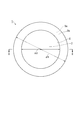
- FIG. 1 is a view showing an embodiment of a dicing / die bonding integrated film according to the present invention.
- FIG. 2 is a cross-sectional view taken along the line II-II in FIG.
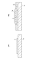
- Fig.3 (a) is a figure which shows a dicing film.
- FIG. 3B is a diagram showing a die bonding film.
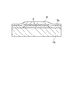
- Fig.4 (a) is a figure which shows the state which pre-cut the adhesive bond layer.
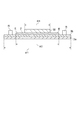
- FIG.4 (b) is a figure which shows the state which affixed the dicing film on the die-bonding film.
- FIG. 5 is a diagram showing a state in which the base film and the pressure-sensitive adhesive layer are pre-cut.
- FIG. 6 is a diagram showing a semiconductor wafer attaching step.
- FIG. 1 is a view showing an embodiment of a dicing / die bonding integrated film according to the present invention.
- FIG. 2 is a cross-sectional view taken along the line II-II
- FIG. 7 is a view showing a state in which a semiconductor wafer is stuck on the adhesive layer.
- FIG. 8 is a diagram showing a state where dicing is performed using the dicing / die bonding integrated film according to the present invention.
- FIG. 9 is a diagram illustrating a state in which the separated semiconductor chip is mounted on the die pad.
- FIG. 10 is a diagram showing a state where dicing is performed using a conventional dicing / die bonding integrated film.
- FIG. 1 is a view showing an embodiment of a dicing / die bonding integrated film 1 according to the present invention.
- FIG. 2 is a cross-sectional view taken along the line II-II in FIG.
- the dicing / die bonding integrated film 1 provides a function as a dicing film for dividing a semiconductor wafer into semiconductor chips and an adhesive layer for connecting the separated semiconductor chips to a die pad. It is the film which has the function to do.
- the dicing / die bonding integrated film 1 includes a base film 3a, an adhesive layer 3b, and an adhesive layer 2.
- the base film 3a is a part that supports the semiconductor wafer during dicing.
- the base film 3a has a circular planar shape, and the diameter ⁇ 1 of the base film 3a is larger than the inner diameter of the annular wafer ring used for dicing.
- Examples of the base film 3a include a polytetrafluoroethylene film, a polyethylene terephthalate film, a film made of a polyvinyl acetate polyethylene copolymer, a polyethylene film, a polypropylene film, a polymethylpentene film, a plastic film such as polyvinyl chloride, and the like. A film or the like obtained by laminating them can be used.
- the pressure-sensitive adhesive layer 3b is a portion to which the wafer ring is attached and fixed.
- the pressure-sensitive adhesive layer 3b has a circular planar shape, and the diameter ⁇ 1 of the pressure-sensitive adhesive layer 3b is larger than the inner diameter of an annular wafer ring used for dicing.
- the thickness of the pressure-sensitive adhesive layer 3b is, for example, about 1 ⁇ m to 50 ⁇ m.
- the pressure-sensitive adhesive layer 3b is a pressure-sensitive type, and is, for example, a pressure-sensitive adhesive layer mainly composed of acrylic, rubber, silicone, polyurethane, or polyester.
- the pressure-sensitive adhesive layer is an adhesive layer that can peel off the adherend without irradiating energy rays. When the pressure-sensitive adhesive layer 3b is a pressure-sensitive type, it is difficult for variations in the adhesive strength of each part on the pressure-sensitive adhesive layer 3b to occur.
- the adhesive layer 2 has a central portion on which a semiconductor wafer to be diced is concentrically attached, and is used for bonding and connecting a semiconductor chip separated after dicing to a die pad.
- the adhesive contained in the adhesive layer 2 include a thermosetting adhesive such as an epoxy resin, a photocurable adhesive, a thermoplastic adhesive, and an oxygen reactive adhesive.
- the adhesive layer 2 has a circular planar shape.
- the area of the adhesive layer 2 is larger than the area of the semiconductor wafer.
- the film thickness of the adhesive layer 2 is, for example, about 1 ⁇ m to 250 ⁇ m. If the thickness of the adhesive layer 2 is less than 1 ⁇ m, it will be difficult to ensure a sufficient adhesive force at the time of die bonding, and if it is greater than 250 ⁇ m, it will be uneconomical and have few advantages in characteristics.
- the diameter ⁇ 2 of the adhesive layer 2 is larger than the diameter of the semiconductor wafer, and the difference between the diameter ⁇ 2 of the adhesive layer 2 and the diameter of the semiconductor wafer is larger than 20 mm and smaller than 35 mm.
- the inner diameter of the wafer ring for blade dicing needs to be large enough that the blade does not touch the wafer ring during blade dicing. For this reason, the inner diameter of the wafer ring is, for example, 45 mm or more larger than the diameter of the semiconductor wafer. It is preferable that the adhesive layer 2 has a size that can surely fit inside the hole of the wafer ring.
- the diameter of the adhesive layer 2 is preferably about 10 mm smaller than the inner diameter of the hole in the wafer ring.
- the dicing / die bonding integrated film 1 is expanded. Since the dicing / die bonding integrated film 1 is expanded, the interval between the semiconductor chips is widened, and the pickup can be easily performed.
- the adhesive layer 2 is preferably about 10 mm smaller than the inner diameter of the hole in the wafer ring.
- the adhesive layer 2 can be surely fit inside the hole of the wafer ring and can sufficiently transmit the stress of the expand. It will be possible.
- the difference between the diameter of the adhesive layer 2 and the diameter of the semiconductor wafer is smaller than 32 mm, the adhesive layer 2 can be more securely accommodated inside the hole of the wafer ring, and more fully transmit the stress of the expand. Will be able to.
- the diameter of the adhesive layer 2 is, for example, not less than 223 mm and less than 248 mm, preferably 228 mm. This is less than 238 mm.
- the diameter of the adhesive layer 2 is, for example, not less than 325 mm and less than 350 mm, preferably It is 330 mm or more and less than 340 mm.
- the dicing / die bonding integrated film 1 is formed by laminating a base film 3a, an adhesive layer 3b, and an adhesive layer 2 in this order. That is, the pressure-sensitive adhesive layer 3b is formed in contact with the base film 3a, and the adhesive layer 2 is formed in contact with the pressure-sensitive adhesive layer 3b.
- the base film 3a, the pressure-sensitive adhesive layer 3b, and the adhesive layer 2 having a circular planar shape are laminated so that the centers of the respective circles overlap. Moreover, the base film 3a and the pressure-sensitive adhesive layer 3b and the adhesive layer 2 are arranged concentrically.
- the base film 3a and the pressure-sensitive adhesive layer 3b have the same diameter ⁇ 1, and the pressure-sensitive adhesive layer 3b has the same area as that of the base film 3a.
- the area of the adhesive layer 2 is smaller than the areas of the pressure-sensitive adhesive layer 3b and the base film 3a.
- the difference between the diameter ⁇ 2 of the adhesive layer 2 and the diameter of the semiconductor wafer is larger than 20 mm and smaller than 35 mm, and the semiconductor wafer is placed at the center of the adhesive layer 2. Is attached concentrically (that is, when the center of the adhesive layer 2 and the center of the semiconductor wafer are overlapped), the entire periphery of the adhesive layer 2 protrudes more than 10 mm from the outside of the semiconductor wafer. become. Therefore, as shown in FIG. 8, when the semiconductor wafer is diced by the dicing blade 30 of the dicing apparatus, the cutting water sprayed from the cutting water supply nozzle 40 is prevented from directly hitting the peripheral edge E of the adhesive layer 2. Is done.
- the peripheral edge portion E of the adhesive layer 2 refers to an outer peripheral portion whose distance from the outer peripheral end of the adhesive layer 2 is about 10 mm or less.
- the periphery of the adhesive layer 2 protrudes from the outside of the semiconductor wafer to be larger than 10 mm over the entire surface. However, if it protrudes larger than 10 mm in the direction in which the cutting water easily hits, the entire periphery is not necessarily larger than 10 mm. There is no need to protrude significantly.
- a blade cooler, shower, and spray are standard equipment.
- the supply pressure of each of the blade cooler, the shower, and the spray is, for example, about 0.2 MPa to 0.6 MPa.
- the flow rates of the blade cooler, shower, and spray are, for example, about 0.5 L / min to 2.0 L / min.
- the semiconductor wafer is placed at the center of the adhesive layer 2.
- the amount of the peripheral edge of the adhesive layer 2 protruding from the outside of the semiconductor wafer is 10 mm or less as a whole.
- the peripheral edge portion E of the adhesive layer 2 is peeled off due to the hydraulic pressure of the cutting water in dicing, and the peeled pieces B of the peeled adhesive layer 2 adhere to the semiconductor wafer.
- the diameter ⁇ 1 of each of the base film 3a and the pressure-sensitive adhesive layer 3b is larger than the inner diameter of the wafer ring used for dicing, and the adhesive layer 2 Is smaller than the inner diameter of the wafer ring, the wafer ring used for dicing can be easily attached to the pressure-sensitive adhesive layer 3b laminated on the base film 3a.
- the present invention is not limited to the dicing / die bonding integrated film 1 described above.
- the planar shape of the adhesive layer 2 is preferably similar to the planar shape of the semiconductor wafer.
- a shape in which a part of the outer periphery of the circle is a straight line may be used.
- the planar shape of the base film 3a and the pressure-sensitive adhesive layer 3b may be other than a circle, for example, a rectangle.
- the diameter of the adhesive layer 3b should just be larger than the internal diameter of the cyclic
- the effect of the present invention is particularly remarkable when the pressure-sensitive adhesive layer 3b is a pressure-sensitive type, but even if the pressure-sensitive adhesive layer 3b is a UV type (which can change the adhesive force by UV irradiation), the present invention The effect is obtained.
- a peelable substrate a long sheet having a width larger than the diameter of the semiconductor wafer to be attached can be used.
- the thickness of the peelable substrate can be appropriately selected within a range that does not impair the workability, and can be, for example, about 1 ⁇ m to 1000 ⁇ m.
- a polyester film, a polyolefin film, a plastic film, or the like can be used.
- the dicing film in which the adhesive layer 3b was formed on the base film 3a is prepared (dicing film preparation process).
- the die bonding film in which the adhesive bond layer 2 was formed on the peelable base material 10 is prepared (die bonding film preparation process).
- the adhesive layer 2 is cut into a circle (adhesive layer cutting step).
- the area of the adhesive layer 2 is larger than the area of the semiconductor wafer attached concentrically to the central portion of the adhesive layer 2 and more than the areas of the adhesive layer 3b and the base film 3a.
- the adhesive layer 2 is cut so as to be smaller.
- the diameter of the adhesive layer 2 is larger than the diameter of the semiconductor wafer and smaller than the inner diameter of the wafer ring used for dicing, and the difference between the diameter of the adhesive layer 2 and the diameter of the semiconductor wafer is 20 mm.
- the adhesive layer 2 is cut into a circle so as to be larger than 35 mm and smaller than 35 mm.
- the base film 3a and the pressure-sensitive adhesive layer 3b are cut into a circle (base film and pressure-sensitive adhesive layer cutting step).
- the base film 3a and the pressure-sensitive adhesive layer 3b are set such that the diameters of the base film 3a and the pressure-sensitive adhesive layer 3b are larger than the inner diameter of the wafer ring used for dicing. Cut into circles.
- size of the planar shape of the base film 3a and the adhesive layer 3b is larger than a wafer ring previously, a base film and an adhesive layer cutting process can be skipped.
- the difference between the diameter ⁇ 2 of the adhesive layer 2 and the diameter of the semiconductor wafer is larger than 20 mm and smaller than 35 mm. Therefore, as described above, when the semiconductor wafer is diced with the dicing blade, the cutting water is prevented from directly hitting the peripheral edge E of the adhesive layer 2. Therefore, peeling of the peripheral edge E of the adhesive layer 2 due to the cutting water load and water pressure in dicing can be suppressed.
- the dicing / die bonding integrated film 1 manufactured by the above-described manufacturing method of the dicing / die bonding integrated film 1 is prepared (preparation step).
- the dicing / die bonding integrated film 1 in which the adhesive layer 2, the pressure-sensitive adhesive layer 3b, and the base film 3a are formed on a long peelable base 10 is used.
- the dicing / die bonding integrated film 1 is wound around a feeding device 11 as shown in FIG.
- the peelable substrate 10 is peeled off (substrate peeling step).
- the semiconductor wafer W is affixed concentrically to the central portion of the adhesive layer 2 on the adhesive layer 2 exposed by peeling the peelable substrate 10 (semiconductor wafer pasting step).
- the entire periphery of the adhesive layer 2 protrudes outside the semiconductor wafer W by more than 10 mm.
- the wafer ring R is stuck to the pressure-sensitive adhesive layer 3b outside the periphery of the adhesive layer 2 (wafer ring sticking step).
- the dicing / die bonding integrated film 1 is fed from the feeding device 11 by the feeding roller 13, and the peelable substrate 10 is peeled by the separation plate 15.
- the adhesive layer 2, the pressure-sensitive adhesive layer 3b, and the base film 3a are separated from the peelable base material 10.
- the separated adhesive layer 2, pressure-sensitive adhesive layer 3 b, and base film 3 a are pressed against the semiconductor wafer W and the wafer ring R on the stage S by the pressing roller 14.
- the semiconductor wafer W is stuck to the adhesive layer 2
- the wafer ring R is stuck to the adhesive layer 3b.
- the peelable substrate 10 that has been peeled off is wound around the winding device 12 by the winding roller 16.
- the semiconductor wafer W attached to the adhesive layer 2 is diced to obtain a plurality of separated semiconductor chips W1 (chip formation step).
- chip formation step cutting water is sprayed onto the dicing blade 30 and the semiconductor wafer W from the cutting water supply nozzle 40 of the dicing apparatus.
- the frictional heat between the semiconductor wafer W and the dicing blade 30 is cooled by the cutting water, and chips and the like of the semiconductor wafer W are cleaned and removed.
- the supply pressures of the blade cooler, shower, and spray that are standard equipment as cutting water are about 0.2 MPa to 0.6 MPa, and the flow rate is about 0.5 L / min to 2.0 L / min. To do.
- the separated semiconductor chip W1 is picked up and mounted on the die pad 7 with the adhesive layer 2a interposed therebetween as shown in FIG. 9 (die bonding step). Then, the semiconductor chip W1 on the die pad 7 is connected to the lead frame lead (wire bonding step). Finally, a lead frame on which the semiconductor chip W1 is mounted is molded with resin or the like (molding process).
- the difference between the diameter ⁇ 2 of the adhesive layer 2 and the diameter of the semiconductor wafer W is larger than 20 mm and smaller than 35 mm. Therefore, as described above, when the semiconductor wafer W is diced with the dicing blade 30, it is suppressed that the cutting water directly hits the peripheral edge E of the adhesive layer 2. Therefore, peeling of the peripheral edge E of the adhesive layer 2 due to the water pressure of the cutting water in dicing can be suppressed. Therefore, the semiconductor chip W1 with less contamination due to the adhesive layer 2 can be obtained.
- Example 1 Comparative Examples 1 and 2 will be described below, but the present invention is not limited to the following examples.
- Example 1 Comparative Examples 1 and 2 will be described below, but the present invention is not limited to the following examples.
- Example 1 shows an example in which a silicon wafer having a thickness of 75 ⁇ m and a diameter of 203 mm (8 inches) and a wafer ring having a diameter of 248 mm or more are used.
- a 300 mm wide dicing film for example, SD-3001 series manufactured by Hitachi Chemical Co., Ltd.
- a die bonding film for example, FH-900 series manufactured by Hitachi Chemical Co., Ltd.
- the adhesive layer was pre-cut (preliminarily cut) so that the planar shape of the adhesive layer of the die bonding film was a circle having a diameter of 223 mm.
- the adhesive layer was pre-cut so that the area of the adhesive layer was larger than the area of the silicon wafer to be diced and smaller than the areas of the pressure-sensitive adhesive layer and the base film.
- the surface on which the pressure-sensitive adhesive layer of the dicing film was formed was attached to the peelable substrate and the pre-cut adhesive layer.
- the base film and the pressure-sensitive adhesive layer were pre-cut (preliminarily cut) so that the planar shape of the base film and the pressure-sensitive adhesive layer was a circle having a diameter of 270 mm, thereby preparing a dicing / die bonding integrated film.
- the circular base film and pressure-sensitive adhesive layer and the circular adhesive layer were concentric.
- the peelable substrate of the dicing / die bonding integrated film was peeled off, and a silicon wafer was laminated on the exposed adhesive layer. Further, the wafer ring was fixed to the adhesive layer. In this state, the silicon wafer was diced using a dicing blade (for example, full auto dicer DFD-6361 manufactured by DISCO Corporation) while spraying cutting water. Dicing was performed by a step cut method in which two dicing blades having different thicknesses were sequentially used.
- a dicing blade for example, full auto dicer DFD-6361 manufactured by DISCO Corporation
- a dicing blade NBC-ZH204J-SE 27HDDD manufactured by DISCO Corporation was used as the first thick dicing blade, and a dicing blade NBC-ZH127F-SE 27HDBB manufactured by DISCO Corporation was used as the second thin dicing blade.
- the blade rotation speed was 40,000 rpm, and the cutting speed was 30 mm / second.
- the blade feed pitch when cutting the silicon wafer, that is, the dicing interval was set to 5 mm.
- the supply pressure of each blade cooler, shower, and spray which is standard equipment as cutting water, is about 0.4 MPa, and each flow rate of the blade cooler, shower, and spray is 1.5 L / min, 1.0 L / min and 1.0 L / min. (Examples 2 to 8)
- Example 2 the conditions were the same as in Example 1 except that the diameter of the adhesive layer of the die bonding film was 225 mm, 228 mm, 230 mm, 233 mm, 235 mm, 238 mm, and 240 mm, respectively.
- the diameter of the adhesive layer of the die bonding film was 225 mm, 228 mm, 230 mm, 233 mm, 235 mm, 238 mm, and 240 mm, respectively.
- Example 9 the conditions were the same as in Example 1 except that the diameter of the adhesive layer of the die bonding film was 220 mm.
- Example 9 a silicon wafer having a thickness of 75 ⁇ m and a diameter of 305 mm (12 inches), a wafer ring having a diameter of 350 mm or more, and a dicing film having a width of 400 mm were used, and the diameter of the adhesive layer of the die bonding film was 325 mm, 327 mm, respectively.
- the conditions were the same as those in Example 1 except that 330 mm, 332 mm, 335 mm, 337 mm, 340 mm, and 342 mm were set. (Comparative Example 2)
- the peripheral portion of the adhesive layer is prevented from peeling off from the pressure-sensitive adhesive layer, the dicing die bonding integrated film, the manufacturing method of the dicing die bonding integrated film, and A semiconductor chip manufacturing method can be provided.
- SYMBOLS 1 Dicing die-bonding integrated film, 2, 2a ... Adhesive layer, 3a ... Base film, 3b ... Adhesive layer, 7 ... Die pad, 10 ... Stripping base material, E ... Peripheral part, W ... Semiconductor wafer , W1 ... semiconductor chip, R ... wafer ring.
Landscapes
- Chemical & Material Sciences (AREA)
- Organic Chemistry (AREA)
- Dicing (AREA)
- Die Bonding (AREA)
- Finish Polishing, Edge Sharpening, And Grinding By Specific Grinding Devices (AREA)
- Adhesive Tapes (AREA)
- Adhesives Or Adhesive Processes (AREA)
Abstract
Description
(実施例1)
(実施例2~8)
(比較例1)
(実施例9~16)
(比較例2)
(評価)


Claims (4)
- 基材フィルムと、
前記基材フィルム上に形成され、ブレードダイシングに用いられるウェハリングが貼付される感圧型の粘着剤層と、
前記粘着剤層上に形成され、ブレードダイシングの対象である半導体ウェハが貼付される中央部を有する接着剤層と、を備え、
前記接着剤層の平面形状は円形となっており、
前記接着剤層の面積は、前記半導体ウェハの面積よりも大きく、かつ前記基材フィルム及び前記粘着剤層のそれぞれの面積よりも小さくなっており、
前記接着剤層の直径は、前記半導体ウェハの直径よりも大きくかつ前記ウェハリングの内径よりも小さくなっており、前記接着剤層の直径と前記半導体ウェハの直径との差が20mmよりも大きく35mmよりも小さくなっていることを特徴とするダイシング・ダイボンディング一体型フィルム。 - 基材フィルム上に粘着剤層が形成されたダイシングフィルムを準備するダイシングフィルム準備工程と、
剥離性基材上に接着剤層が形成されたダイボンディングフィルムを準備するダイボンディングフィルム準備工程と、
前記接着剤層の面積が、前記接着剤層の中央部に貼付される半導体ウェハの面積よりも大きく、かつ前記粘着剤層及び前記基材フィルムのそれぞれの面積よりも小さくなるように、前記接着剤層を円形に切断する接着剤層切断工程と、
前記ダイシングフィルムの前記粘着剤層が形成された面を、前記ダイボンディングフィルムの前記剥離性基材及び前記円形に切断された接着剤層に貼り付けるフィルム貼付工程と、を備え、
前記接着剤層切断工程において、
前記接着剤層の直径が、前記半導体ウェハの直径よりも大きくかつブレードダイシングに用いられるウェハリングの内径よりも小さくなり、前記接着剤層の直径と前記半導体ウェハの直径との差が20mmよりも大きく35mmよりも小さくなるように、前記接着剤層を切断することを特徴とするダイシング・ダイボンディング一体型フィルムの製造方法。 - 前記ダイシングフィルム準備工程では、基材フィルム上に感圧型の粘着剤層が形成されたダイシングフィルムを準備することを特徴とする請求項2記載のダイシング・ダイボンディング一体型フィルムの製造方法。
- 基材フィルム上に粘着剤層が形成され、前記粘着剤層上に接着剤層が形成されたダイシング・ダイボンディング一体型フィルムの前記接着剤層に、前記接着剤層の周縁が全体にわたって10mmよりも大きくはみ出るように、半導体ウェハを貼付する半導体ウェハ貼付工程と、
前記接着剤層の周縁の外側で、ウェハリングを前記粘着剤層に貼付する半導体ウェハ貼付工程と、
前記半導体ウェハをブレードダイシングし、個片化された複数の半導体チップを得るチップ化工程とを備えることを特徴とする半導体チップの製造方法。
Priority Applications (4)
| Application Number | Priority Date | Filing Date | Title |
|---|---|---|---|
| JP2012524577A JP5833005B2 (ja) | 2010-07-13 | 2011-07-13 | ダイシング・ダイボンディング一体型フィルム |
| KR1020137003315A KR101521727B1 (ko) | 2010-07-13 | 2011-07-13 | 다이싱·다이 본딩 일체형 필름, 다이싱·다이 본딩 일체형 필름의 제조 방법, 및 반도체 칩의 제조 방법 |
| CN201180034409.XA CN103109353B (zh) | 2010-07-13 | 2011-07-13 | 切割-芯片焊接一体型膜及其制造方法、半导体芯片的制造方法 |
| US13/809,816 US8975161B2 (en) | 2010-07-13 | 2011-07-13 | Dicing/die bonding integral film, dicing/die bonding integral film manufacturing method, and semiconductor chip manufacturing method |
Applications Claiming Priority (2)
| Application Number | Priority Date | Filing Date | Title |
|---|---|---|---|
| JP2010-159030 | 2010-07-13 | ||
| JP2010159030 | 2010-07-13 |
Publications (1)
| Publication Number | Publication Date |
|---|---|
| WO2012008491A1 true WO2012008491A1 (ja) | 2012-01-19 |
Family
ID=45469488
Family Applications (1)
| Application Number | Title | Priority Date | Filing Date |
|---|---|---|---|
| PCT/JP2011/065986 Ceased WO2012008491A1 (ja) | 2010-07-13 | 2011-07-13 | ダイシング・ダイボンディング一体型フィルム、ダイシング・ダイボンディング一体型フィルムの製造方法、及び半導体チップの製造方法 |
Country Status (6)
| Country | Link |
|---|---|
| US (1) | US8975161B2 (ja) |
| JP (2) | JP5833005B2 (ja) |
| KR (1) | KR101521727B1 (ja) |
| CN (1) | CN103109353B (ja) |
| TW (1) | TWI460779B (ja) |
| WO (1) | WO2012008491A1 (ja) |
Cited By (3)
| Publication number | Priority date | Publication date | Assignee | Title |
|---|---|---|---|---|
| JP2014192462A (ja) * | 2013-03-28 | 2014-10-06 | Lintec Corp | 樹脂膜形成用シート |
| JP2022174548A (ja) * | 2021-05-11 | 2022-11-24 | 株式会社ディスコ | ウェーハの加工方法 |
| JP2023148120A (ja) * | 2022-03-30 | 2023-10-13 | 株式会社ディスコ | はみ出し部除去機構及びエキスパンド装置 |
Families Citing this family (14)
| Publication number | Priority date | Publication date | Assignee | Title |
|---|---|---|---|---|
| KR102029861B1 (ko) * | 2013-07-24 | 2019-11-08 | 엘지이노텍 주식회사 | 발광 소자 제조 방법, 발광 소자 제조 장치 및 이에 의해 제조된 발광 소자 |
| US9299614B2 (en) * | 2013-12-10 | 2016-03-29 | Applied Materials, Inc. | Method and carrier for dicing a wafer |
| US20170213765A1 (en) * | 2014-05-23 | 2017-07-27 | Hitachi Chemical Company, Ltd. | Die bonding/dicing sheet |
| JP7130323B2 (ja) | 2018-05-14 | 2022-09-05 | 株式会社ディスコ | ウェーハの加工方法 |
| JP7281873B2 (ja) * | 2018-05-14 | 2023-05-26 | 株式会社ディスコ | ウェーハの加工方法 |
| WO2019220599A1 (ja) * | 2018-05-17 | 2019-11-21 | 日立化成株式会社 | ダイシング・ダイボンディング一体型フィルム及びその製造方法、並びに、半導体装置の製造方法 |
| JP7139047B2 (ja) * | 2018-07-06 | 2022-09-20 | 株式会社ディスコ | ウェーハの加工方法 |
| US11031311B2 (en) * | 2018-11-21 | 2021-06-08 | Texas Instruments Incorporated | Packaged semiconductor device with multilayer stress buffer |
| SG11202112361PA (en) * | 2019-05-10 | 2021-12-30 | Showa Denko Materials Co Ltd | Method for evaluating pickability, film for combined dicing and die bonding, method for evaluating and method for classifying film for combined dicing and die bonding, and method for manufacturing semiconductor device |
| WO2020230209A1 (ja) | 2019-05-10 | 2020-11-19 | 昭和電工マテリアルズ株式会社 | ピックアップ性の評価方法、ダイシング・ダイボンディング一体型フィルム、ダイシング・ダイボンディング一体型フィルムの評価方法及び選別方法、並びに半導体装置の製造方法 |
| JP7008164B1 (ja) * | 2020-07-30 | 2022-01-25 | 古河電気工業株式会社 | 半導体加工用テープ |
| CN112201600B (zh) * | 2020-10-14 | 2024-03-08 | 北京中科镭特电子有限公司 | 一种晶圆劈裂扩片装置及晶圆裂片扩片方法 |
| CN114479705B (zh) * | 2022-01-20 | 2023-11-07 | 三星半导体(中国)研究开发有限公司 | 晶圆贴合膜及其制造方法 |
| JP2024050022A (ja) * | 2022-09-29 | 2024-04-10 | 株式会社ディスコ | 切削装置及び切削方法 |
Citations (7)
| Publication number | Priority date | Publication date | Assignee | Title |
|---|---|---|---|---|
| JPS59177942A (ja) * | 1983-03-28 | 1984-10-08 | Nitto Electric Ind Co Ltd | ウエハ固定方法 |
| JPH08213349A (ja) * | 1994-11-29 | 1996-08-20 | Lintec Corp | ダイシング用リングフレームへの接着剤の付着防止方法、該方法に用いられる粘着シートおよび該粘着シートを備えたウェハ加工用シート |
| WO2008105169A1 (ja) * | 2007-02-28 | 2008-09-04 | Sumitomo Bakelite Co., Ltd. | 半導体用接着フィルムおよびそれを用いた半導体装置 |
| JP2008211224A (ja) * | 2008-03-17 | 2008-09-11 | Sumitomo Bakelite Co Ltd | ダイシングシート機能付きダイアタッチフィルム及びそれを用いた半導体装置の製造方法 |
| JP2009032799A (ja) * | 2007-07-25 | 2009-02-12 | Lintec Corp | ウェハ加工用テープ |
| JP2009094127A (ja) * | 2007-10-04 | 2009-04-30 | Furukawa Electric Co Ltd:The | 半導体ウエハ加工用フィルム |
| JP2011142206A (ja) * | 2010-01-07 | 2011-07-21 | Sekisui Chem Co Ltd | ダイシング−ダイボンディングテープ及びその製造方法 |
Family Cites Families (22)
| Publication number | Priority date | Publication date | Assignee | Title |
|---|---|---|---|---|
| JPH0715087B2 (ja) | 1988-07-21 | 1995-02-22 | リンテック株式会社 | 粘接着テープおよびその使用方法 |
| JP2860131B2 (ja) * | 1990-02-06 | 1999-02-24 | 株式会社ディスコ | ダイシング装置 |
| MY118036A (en) * | 1996-01-22 | 2004-08-30 | Lintec Corp | Wafer dicing/bonding sheet and process for producing semiconductor device |
| JP3592018B2 (ja) * | 1996-01-22 | 2004-11-24 | 日本テキサス・インスツルメンツ株式会社 | ポリイミド接着シートおよびポリイミド用工程フィルム |
| JPH10335271A (ja) * | 1997-06-02 | 1998-12-18 | Texas Instr Japan Ltd | ウェハ貼着用シートおよび半導体装置の製造方法 |
| JP3578592B2 (ja) | 1997-06-03 | 2004-10-20 | 住友ベークライト株式会社 | 半導体用ダイアタッチ樹脂ペースト |
| JP4240711B2 (ja) * | 1999-12-27 | 2009-03-18 | 日立化成工業株式会社 | ダイボンディング用接着フィルム及び半導体装置の製造方法 |
| JP2002158276A (ja) | 2000-11-20 | 2002-05-31 | Hitachi Chem Co Ltd | ウエハ貼着用粘着シートおよび半導体装置 |
| JP2002226796A (ja) | 2001-01-29 | 2002-08-14 | Hitachi Chem Co Ltd | ウェハ貼着用粘着シート及び半導体装置 |
| JP4283596B2 (ja) * | 2003-05-29 | 2009-06-24 | 日東電工株式会社 | チップ状ワークの固定方法 |
| JP2005060435A (ja) * | 2003-08-14 | 2005-03-10 | Three M Innovative Properties Co | 両面粘着シート |
| JP4691365B2 (ja) | 2005-02-04 | 2011-06-01 | 株式会社巴川製紙所 | 半導体装置用接着剤組成物および半導体装置用接着シート |
| JP4839629B2 (ja) | 2005-02-18 | 2011-12-21 | 日立化成工業株式会社 | フィルム状接着剤、接着シート及びそれを使用した半導体装置 |
| JP2006232985A (ja) | 2005-02-24 | 2006-09-07 | Shin Etsu Chem Co Ltd | 非ハロゲン系接着剤組成物ならびにそれを用いたカバーレイフィルムおよび接着シート |
| JP4650024B2 (ja) | 2005-02-28 | 2011-03-16 | 住友ベークライト株式会社 | ダイシングシート機能付きダイアタッチフィルム及びそれを用いた半導体装置の製造方法及び半導体装置。 |
| JP2007019151A (ja) * | 2005-07-06 | 2007-01-25 | Furukawa Electric Co Ltd:The | ウエハ加工用テープおよびそれを用いたチップの製造方法 |
| KR100593814B1 (ko) * | 2005-12-06 | 2006-06-28 | 에이스 인더스트리 주식회사 | 반도체 다이본딩용 점착테이프 |
| JP5157208B2 (ja) * | 2006-03-20 | 2013-03-06 | 日立化成株式会社 | ダイボンドダイシングシート |
| WO2008047610A1 (en) | 2006-10-06 | 2008-04-24 | Sumitomo Bakelite Company Limited | Film for semiconductor, method for producing film for semiconductor, and semiconductor device |
| JP4822532B2 (ja) | 2006-11-27 | 2011-11-24 | 日東電工株式会社 | ダイシング・ダイボンドフィルム |
| TW200842174A (en) * | 2006-12-27 | 2008-11-01 | Cheil Ind Inc | Composition for pressure sensitive adhesive film, pressure sensitive adhesive film, and dicing die bonding film including the same |
| JP5757625B2 (ja) | 2008-04-25 | 2015-07-29 | エルジー・ケム・リミテッド | エポキシ系組成物、接着フィルム、ダイシングダイボンディングフィルム及び半導体装置 |
-
2011
- 2011-07-13 CN CN201180034409.XA patent/CN103109353B/zh active Active
- 2011-07-13 US US13/809,816 patent/US8975161B2/en active Active
- 2011-07-13 WO PCT/JP2011/065986 patent/WO2012008491A1/ja not_active Ceased
- 2011-07-13 TW TW100124757A patent/TWI460779B/zh active
- 2011-07-13 KR KR1020137003315A patent/KR101521727B1/ko active Active
- 2011-07-13 JP JP2012524577A patent/JP5833005B2/ja active Active
-
2014
- 2014-12-03 JP JP2014245216A patent/JP5979207B2/ja active Active
Patent Citations (7)
| Publication number | Priority date | Publication date | Assignee | Title |
|---|---|---|---|---|
| JPS59177942A (ja) * | 1983-03-28 | 1984-10-08 | Nitto Electric Ind Co Ltd | ウエハ固定方法 |
| JPH08213349A (ja) * | 1994-11-29 | 1996-08-20 | Lintec Corp | ダイシング用リングフレームへの接着剤の付着防止方法、該方法に用いられる粘着シートおよび該粘着シートを備えたウェハ加工用シート |
| WO2008105169A1 (ja) * | 2007-02-28 | 2008-09-04 | Sumitomo Bakelite Co., Ltd. | 半導体用接着フィルムおよびそれを用いた半導体装置 |
| JP2009032799A (ja) * | 2007-07-25 | 2009-02-12 | Lintec Corp | ウェハ加工用テープ |
| JP2009094127A (ja) * | 2007-10-04 | 2009-04-30 | Furukawa Electric Co Ltd:The | 半導体ウエハ加工用フィルム |
| JP2008211224A (ja) * | 2008-03-17 | 2008-09-11 | Sumitomo Bakelite Co Ltd | ダイシングシート機能付きダイアタッチフィルム及びそれを用いた半導体装置の製造方法 |
| JP2011142206A (ja) * | 2010-01-07 | 2011-07-21 | Sekisui Chem Co Ltd | ダイシング−ダイボンディングテープ及びその製造方法 |
Cited By (5)
| Publication number | Priority date | Publication date | Assignee | Title |
|---|---|---|---|---|
| JP2014192462A (ja) * | 2013-03-28 | 2014-10-06 | Lintec Corp | 樹脂膜形成用シート |
| JP2022174548A (ja) * | 2021-05-11 | 2022-11-24 | 株式会社ディスコ | ウェーハの加工方法 |
| JP7713313B2 (ja) | 2021-05-11 | 2025-07-25 | 株式会社ディスコ | ウェーハの加工方法 |
| JP2023148120A (ja) * | 2022-03-30 | 2023-10-13 | 株式会社ディスコ | はみ出し部除去機構及びエキスパンド装置 |
| JP7781008B2 (ja) | 2022-03-30 | 2025-12-05 | 株式会社ディスコ | はみ出し部除去機構及びエキスパンド装置 |
Also Published As
| Publication number | Publication date |
|---|---|
| CN103109353B (zh) | 2015-11-25 |
| JP5833005B2 (ja) | 2015-12-16 |
| JP2015043471A (ja) | 2015-03-05 |
| JPWO2012008491A1 (ja) | 2013-09-09 |
| TW201205662A (en) | 2012-02-01 |
| TWI460779B (zh) | 2014-11-11 |
| KR101521727B1 (ko) | 2015-05-19 |
| JP5979207B2 (ja) | 2016-08-24 |
| CN103109353A (zh) | 2013-05-15 |
| KR20130051475A (ko) | 2013-05-20 |
| US20130143390A1 (en) | 2013-06-06 |
| US8975161B2 (en) | 2015-03-10 |
Similar Documents
| Publication | Publication Date | Title |
|---|---|---|
| JP5833005B2 (ja) | ダイシング・ダイボンディング一体型フィルム | |
| JP3521099B2 (ja) | ダイシング用リングフレームへの接着剤の付着防止用粘着シートおよび該粘着シートを備えたウェハ加工用シート | |
| CN205004316U (zh) | 芯片接合切割片材 | |
| CN103155109B (zh) | 晶圆加工用胶带、晶圆加工用胶带的制造方法以及半导体装置的制造方法 | |
| JP2005162818A (ja) | ダイシングダイボンドシート | |
| WO2008047708A1 (en) | Sheet for die sort and method of transferring chip with adhesive layer | |
| JPWO2011007732A1 (ja) | 接着シートの製造方法及び接着シート | |
| JP4505798B2 (ja) | 粘接着シート | |
| JP5323331B2 (ja) | ウェハ加工用シート | |
| JP5666659B2 (ja) | ウェハ加工用シート | |
| JP2008066336A (ja) | ウエハ加工用シート | |
| JP2013021109A (ja) | 粘着シート及び粘着シートを用いた円板状被加工物の加工方法 | |
| JP2005116790A (ja) | 半導体素子製造用工程フィルム、及びダイシング・ダイボンド一体型テープ | |
| JP2017139409A (ja) | ダイボンドダイシングシート | |
| JP2015076422A (ja) | 粘接着剤層付き半導体チップの製造方法 | |
| JP2007036074A (ja) | 半導体装置の製造方法 | |
| JP2011198797A (ja) | ダイボンドダイシングシート及び半導体チップの製造方法 | |
| JP2009032799A (ja) | ウェハ加工用テープ | |
| JP2009260047A (ja) | ダイソート用シート | |
| JP2012169337A (ja) | ダイシング・ダイボンディング一体型シート、およびその製造方法 | |
| JP2012253286A (ja) | ウェハ加工用テープ、ウェハ加工用テープの製造方法、及び半導体装置の製造方法 | |
| JP2013006925A (ja) | 接着シート | |
| JP2014022513A (ja) | ウェハ加工用テープ |
Legal Events
| Date | Code | Title | Description |
|---|---|---|---|
| WWE | Wipo information: entry into national phase |
Ref document number: 201180034409.X Country of ref document: CN |
|
| 121 | Ep: the epo has been informed by wipo that ep was designated in this application |
Ref document number: 11806821 Country of ref document: EP Kind code of ref document: A1 |
|
| WWE | Wipo information: entry into national phase |
Ref document number: 2012524577 Country of ref document: JP |
|
| NENP | Non-entry into the national phase |
Ref country code: DE |
|
| ENP | Entry into the national phase |
Ref document number: 20137003315 Country of ref document: KR Kind code of ref document: A |
|
| WWE | Wipo information: entry into national phase |
Ref document number: 13809816 Country of ref document: US |
|
| 122 | Ep: pct application non-entry in european phase |
Ref document number: 11806821 Country of ref document: EP Kind code of ref document: A1 |