WO2011132275A1 - 電流共振電源 - Google Patents
電流共振電源 Download PDFInfo
- Publication number
- WO2011132275A1 WO2011132275A1 PCT/JP2010/057065 JP2010057065W WO2011132275A1 WO 2011132275 A1 WO2011132275 A1 WO 2011132275A1 JP 2010057065 W JP2010057065 W JP 2010057065W WO 2011132275 A1 WO2011132275 A1 WO 2011132275A1
- Authority
- WO
- WIPO (PCT)
- Prior art keywords
- current
- voltage
- power supply
- transformer
- input
- Prior art date
- Legal status (The legal status is an assumption and is not a legal conclusion. Google has not performed a legal analysis and makes no representation as to the accuracy of the status listed.)
- Ceased
Links
Images



Classifications
-
- H—ELECTRICITY
- H02—GENERATION; CONVERSION OR DISTRIBUTION OF ELECTRIC POWER
- H02M—APPARATUS FOR CONVERSION BETWEEN AC AND AC, BETWEEN AC AND DC, OR BETWEEN DC AND DC, AND FOR USE WITH MAINS OR SIMILAR POWER SUPPLY SYSTEMS; CONVERSION OF DC OR AC INPUT POWER INTO SURGE OUTPUT POWER; CONTROL OR REGULATION THEREOF
- H02M3/00—Conversion of DC power input into DC power output
- H02M3/22—Conversion of DC power input into DC power output with intermediate conversion into AC
- H02M3/24—Conversion of DC power input into DC power output with intermediate conversion into AC by static converters
- H02M3/28—Conversion of DC power input into DC power output with intermediate conversion into AC by static converters using discharge tubes with control electrode or semiconductor devices with control electrode to produce the intermediate AC
- H02M3/325—Conversion of DC power input into DC power output with intermediate conversion into AC by static converters using discharge tubes with control electrode or semiconductor devices with control electrode to produce the intermediate AC using devices of a triode or a transistor type requiring continuous application of a control signal
- H02M3/335—Conversion of DC power input into DC power output with intermediate conversion into AC by static converters using discharge tubes with control electrode or semiconductor devices with control electrode to produce the intermediate AC using devices of a triode or a transistor type requiring continuous application of a control signal using semiconductor devices only
- H02M3/337—Conversion of DC power input into DC power output with intermediate conversion into AC by static converters using discharge tubes with control electrode or semiconductor devices with control electrode to produce the intermediate AC using devices of a triode or a transistor type requiring continuous application of a control signal using semiconductor devices only in push-pull configuration
- H02M3/3376—Conversion of DC power input into DC power output with intermediate conversion into AC by static converters using discharge tubes with control electrode or semiconductor devices with control electrode to produce the intermediate AC using devices of a triode or a transistor type requiring continuous application of a control signal using semiconductor devices only in push-pull configuration with automatic control of output voltage or current
-
- H—ELECTRICITY
- H02—GENERATION; CONVERSION OR DISTRIBUTION OF ELECTRIC POWER
- H02M—APPARATUS FOR CONVERSION BETWEEN AC AND AC, BETWEEN AC AND DC, OR BETWEEN DC AND DC, AND FOR USE WITH MAINS OR SIMILAR POWER SUPPLY SYSTEMS; CONVERSION OF DC OR AC INPUT POWER INTO SURGE OUTPUT POWER; CONTROL OR REGULATION THEREOF
- H02M1/00—Details of apparatus for conversion
- H02M1/32—Means for protecting converters other than automatic disconnection
-
- H—ELECTRICITY
- H02—GENERATION; CONVERSION OR DISTRIBUTION OF ELECTRIC POWER
- H02M—APPARATUS FOR CONVERSION BETWEEN AC AND AC, BETWEEN AC AND DC, OR BETWEEN DC AND DC, AND FOR USE WITH MAINS OR SIMILAR POWER SUPPLY SYSTEMS; CONVERSION OF DC OR AC INPUT POWER INTO SURGE OUTPUT POWER; CONTROL OR REGULATION THEREOF
- H02M1/00—Details of apparatus for conversion
- H02M1/0048—Circuits or arrangements for reducing losses
- H02M1/0054—Transistor switching losses
- H02M1/0058—Transistor switching losses by employing soft switching techniques, i.e. commutation of transistors when applied voltage is zero or when current flow is zero
-
- Y—GENERAL TAGGING OF NEW TECHNOLOGICAL DEVELOPMENTS; GENERAL TAGGING OF CROSS-SECTIONAL TECHNOLOGIES SPANNING OVER SEVERAL SECTIONS OF THE IPC; TECHNICAL SUBJECTS COVERED BY FORMER USPC CROSS-REFERENCE ART COLLECTIONS [XRACs] AND DIGESTS
- Y02—TECHNOLOGIES OR APPLICATIONS FOR MITIGATION OR ADAPTATION AGAINST CLIMATE CHANGE
- Y02B—CLIMATE CHANGE MITIGATION TECHNOLOGIES RELATED TO BUILDINGS, e.g. HOUSING, HOUSE APPLIANCES OR RELATED END-USER APPLICATIONS
- Y02B70/00—Technologies for an efficient end-user side electric power management and consumption
- Y02B70/10—Technologies improving the efficiency by using switched-mode power supplies [SMPS], i.e. efficient power electronics conversion e.g. power factor correction or reduction of losses in power supplies or efficient standby modes
Definitions
- the present invention relates to a current resonance type power supply device.
- a current as an example of a power supply apparatus that outputs a stable DC voltage via an insulation type transformer by switching a voltage obtained by rectifying and smoothing an AC voltage (hereinafter, AC input voltage) input from a commercial power supply with a switching element A resonant switching power supply is known.
- a circuit for detecting an overcurrent on the primary side of a transformer is generally provided.
- the purpose of detecting an overcurrent is to protect an element such as a FET as a switching element, a transformer, and a capacitor for current resonance from an overcurrent state. Since the lower the input AC voltage from the commercial power supply, the output on the secondary side of the transformer is maintained constant, the on time of the FET becomes longer, the current on the primary side of the transformer becomes higher, and the primary side is an overcurrent It will be in the state. When the primary side of the transformer is in an overcurrent state, there is a concern that the current may flow over the rating (withstand voltage) of the element including the FET on the primary side and the element may be broken. It is necessary to protect the elements on the primary side by stopping.
- Patent Document 1 provides a capacitor for current detection connected in parallel with a capacitor for current resonance, and converts the current flowing in the capacitor for current detection into a voltage. A method of detecting an over current has been proposed.
- the overcurrent detection method described in Patent Document 1 detects the current on the primary side of the transformer, when the input AC voltage fluctuates, the detected current fluctuates due to the overcurrent. . For example, when the input AC voltage is lowered, the detected current value is increased. That is, the current flowing through the current detection capacitor is increased.
- a resistor for current detection may be provided to detect an overcurrent, but even with this method, the current flowing through the current detection resistor becomes large.
- the present invention aims to correctly detect the overcurrent even if the input AC voltage fluctuates.
- a power supply according to the present invention for achieving the above object comprises: a transformer having a primary winding and a secondary winding; two switching elements connected to one end of the primary winding and arranged in series; By alternately operating a resonant capacitor connected to the other end of the primary winding and the two switching elements, the primary winding and the resonant capacitor are caused to resonate, and an alternating voltage is applied to the secondary winding.
- Induced current resonant power supply A current detection unit connected between the other end of the primary winding and the resonance capacitor and detecting a current flowing to the primary side of the transformer; one end of the primary winding and the two switching elements And a current correction unit connected between the current correction units for correcting the current detected by the current detection unit according to a change in voltage input to the primary side of the transformer, and based on an output from the current correction unit.
- the current resonant power supply is controlled.
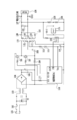
- the circuit diagram of the current resonance power supply device of Example 1 Feature of Circuit of Current Resonant Power Supply Device of Example 1 Voltage waveform when the circuit of Example 1 operates Table showing the relationship of voltage waveforms in FIG. 3
- the circuit diagram and the comparison circuit diagram of the current resonance power supply device of Example 2 The circuit diagram and the comparison circuit diagram of the current resonance power supply device of the third embodiment An example of a circuit diagram of a conventional current resonant power supply An example of a circuit diagram of a conventional current resonant power supply
- a current resonance power supply device (Operation of power supply unit of current resonance type) First, the basic operation of the current resonance type power supply device (hereinafter referred to as a current resonance power supply device) will be described using the circuit diagram shown in FIG.
- 101 is an inlet
- 102 is a fuse
- 103 is a common mode coil
- 104 is a rectifying diode bridge
- 105 is a primary smoothing capacitor
- 106 and 107 are FETs as switching elements.
- 108 is a capacitor for current resonance
- 109 is a resistor for current detection
- 110 is a control IC for controlling the operation of the power supply
- 111 is a start resistor
- 112 is a resistor
- 113 is a diode
- 114 is a capacitor
- 115 is a transformer
- 116 is a primary winding of the transformer 115
- 117 is an auxiliary winding of the transformer 115
- 118 and 119 are secondary windings of the transformer 115
- 120 and 121 are rectifying diodes
- 122 is a smoothing capacitor
- 123 is a photocoupler
- 124 is Shunt regulators 125 and 126 are regulation resistors
- 127 is a voltage output unit
- 128 is a load connected to the power supply.
- the power supply control IC 110 controls the on / off periods of control signals applied to the gate terminals of the FET 106 and the FET 107 so that the DC voltage output from the voltage output unit 127 is constant.
- a voltage obtained by rectifying and smoothing the auxiliary winding 117 of the transformer 115 by a rectifying and smoothing circuit including a resistor 112, a diode 113 and a capacitor 114 is supplied.
- alternating current flows alternately in the forward and reverse directions in the primary winding 116 of the transformer 115 to induce an alternating voltage in the secondary windings 118 and 119 of the transformer 115.
- the induced voltage is rectified and smoothed by a rectifying and smoothing circuit composed of two rectifying diodes 120 and 121 and a smoothing capacitor 122, and a DC voltage is output from the voltage output unit 127.
- the voltage of the voltage output unit 127 is divided by the regulation resistors 125 and 126, and the divided voltage is input to the shunt regulator 124. Then, a feedback signal according to the voltage input to the shunt regulator 124 is generated, and is fed back to the FB terminal of the power supply control IC 110 via the photocoupler 123. Then, the power control IC 110 controls the timing of the switching operation of the FETs 106 and 107 based on the feedback signal, and a stable desired DC voltage is output from the voltage output unit 127.
- an alternating voltage is also induced in the auxiliary winding 117 of the transformer 115, and this induced voltage is rectified and smoothed by the resistor 112, the diode 113 and the capacitor 114 and supplied as a power supply voltage for driving the power control IC 110.
- Ru As described above, when power is supplied from the auxiliary winding 117 of the transformer 115 as a power supply for driving the power control IC 110, the power is not supplied from the startup resistor 111.
- the above-described current detection resistor 109 is provided to detect an overcurrent. Further, as a configuration for detecting an overcurrent, a configuration for detecting by providing a capacitor 201 for current detection described in Patent Document 1 is as shown in FIG.
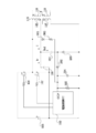
- FIG. 1 is a circuit diagram of a current resonance type power supply device (hereinafter referred to as a current resonance power supply device) according to a first embodiment.
- the overcurrent detection circuit is different in that it is configured by two circuits of a current detection circuit described below and an input AC voltage correction circuit.
- the current resonant power supply device in the current resonant power supply device according to this embodiment, two FETs connected to the primary side of the transformer are alternately operated to resonate the primary winding of the transformer with the resonant capacitor, It is a power supply that induces an alternating voltage on its secondary side.
- the description of the configuration common to FIG. 8 will be omitted.
- the current detection circuit is formed of a circuit including the capacitor 201, the diodes 202 and 203, and the capacitor 204 in FIG. 1, and functions as a current detection unit on the primary side of the transformer.
- the capacitor 201 is connected to one end of the primary winding on the primary side of the transformer 115 (the side to which the resonance capacitor 108 is connected), and the diodes 202 and 203 and the capacitor 204 are connected to each other.
- the detected value is input to.
- the input AC voltage correction circuit is formed of a circuit including a diode 301, resistors 302 and 205, and a capacitor 204 (shared with the current detection circuit), and functions as a current correction unit for the current detected by the current detection circuit.
- the diode 301 and the resistor 302 are connected to the other end of the primary winding of the primary side of the transformer 115 (the side connected to the FETs 106 and 107 arranged in series), and the current detection circuit to the OCP terminal of the power control IC Connected between.
- the current control IC functions as a control unit that controls the on / off operation of the FETs 106 and 107 as in FIG.
- the input AC voltage correction circuit is ignored as the overcurrent detection circuit and the operation is performed only by the current detection circuit is considered.
- the voltage at the OCP terminal of the power control IC 110 is in inverse proportion to the input AC voltage. This is because the conversion efficiency between the primary side and the secondary side is the same, and in the case where the secondary side outputs constant power, the power control IC 110 includes FETs 106 and 107 so that the power on the primary side also becomes constant. This is to control the switching frequency.
- the current flowing to the primary side mainly the current flowing to the FETs 106 and 107, the primary winding 116 of the transformer 115, and the capacitor 201 decreases, and as a result, the OCP terminal of the power control IC 110
- the power on the primary side is controlled.
- the voltage detection circuit is ignored as the overcurrent detection circuit and the operation is performed only with the input AC correction circuit.
- the voltage at the OCP terminal of the power control IC 110 is in proportion to the input AC voltage. This is because the voltage at the OCP terminal of the power supply control IC depends on the input AC voltage.
- FIG. 2 is a view showing a current resonance converter portion of the current resonance power supply device in FIG.
- the current flowing out of the primary winding 116 of the transformer 115 through the FET 106 flows out of the primary winding 116 of the transformer 115 and the current flowing in the resonant capacitor 108 is Ir, the primary winding 116 of the transformer 115
- Icd The current flowing out of the capacitor 201 to the capacitor 201 is denoted by Icd.
- Icd is shown by Formula 1 below.
- Icd (Ccd / (Ccd + Cr)) ⁇ I ⁇ ⁇ ⁇ Formula 1 Cr: electrostatic capacitance of the current resonance capacitor 108
- Ccd electrostatic capacitance of the capacitor 201
- the input AC voltage correction circuit is disregarded as an overcurrent detection circuit, and this current is considered when only the operation of the current detection circuit is considered.
- the voltage Vcd generated across the resistor 205 by Icd is expressed by Equation 2 below.
- Vcd Icd ⁇ Rcd ⁇ Formula 2
- Rcd resistance value of the resistor 205 (however, when the resistance component after the OCP terminal is ignored)
- Ipeak can be expressed by the following Equations 3, 4, and 5.
- Vdch Vdch: positive terminal voltage of the primary electrolytic capacitor 105
- f Switching frequency of the switching FETs 106 and 107 controlled by the power control IC 110
- the power control IC 110 controls the switching frequency of the FETs 106 and 107 such that Ipeak is Ipeak ⁇ 1 / Vdch, that is, Ipeak ⁇ 1 / AC input voltage. This is because the power control IC 110 controls the switching frequency of the FETs 106 and 107 so that when the secondary side outputs a constant power as described above, the power on the primary side also becomes constant. For example, if the input AC voltage is high, the switching frequency of the switching FETs 106 and 107 is controlled to reduce the current flowing to the primary side. Also, if the input AC voltage is low, the switching frequency of the switching FETs 106 and 107 is controlled to increase the current flowing to the primary side. From this, since the relationship of I ⁇ 1 / input AC voltage also holds, the relationship of Icd ⁇ 1 / input AC voltage and Vcd ⁇ 1 / input AC voltage holds from Equation 1.
- Vacr ((R205 / (R205 + R302)) ⁇ Vdch ⁇ On_DUTY) / (On_DUTY + R / R 205 ⁇ Off_DUTY) Equation 6
- R205 resistance value of resistance 205
- R302 resistance value of resistance 302
- Vdch + terminal voltage of primary electrolytic capacitor 105
- ON_DUTY duty ratio when switching FET 107 is ON state
- OFF_DUTY DUTY ratio when the switching FET 107 is in the off state (however, when the forward voltage of the diode 301 is ignored).
- Vocp is a voltage shown in the following Expression 8.
- the overcurrent protection operation is an operation of stopping the operation of the FETs 106 and 107 when the current value input to the OCP terminal becomes equal to or more than a preset threshold value (current value for circuit protection).
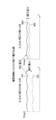
- FIG. 3 shows the voltage Vocp at the OCP terminal of the power supply control IC for the case where the current of the load 128 is the same and the input AC voltage is different, and for each case with or without the input AC voltage correction circuit described above.
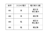
- ⁇ Waveform 401 It is a waveform of Vocp when the input AC voltage is high and there is an input AC voltage correction circuit.
- ⁇ Waveform 402 It is a waveform of Vocp in case input AC voltage is high and there is no input AC voltage correction circuit.
- ⁇ Waveform 403 It is a waveform of Vocp when the input AC voltage is low and there is an input AC voltage correction circuit.
- ⁇ Waveform 404 It is a waveform of Vocp in case input AC voltage is low and there is no input AC voltage correction circuit.
- the waveform 401 is a waveform in which the input AC correction voltage is added to the waveform 402.
- the correction amount at this time is large because the input AC voltage is high.
- the waveform 403 is a waveform in which the input AC correction voltage is added to the waveform 404.
- the correction amount at this time is small because the input AC voltage is low.
- the voltages of the waveform 401 and the waveform 403 to which the input AC correction voltage is added have the same value.
- Vocp regardless of the input AC voltage, the current of the load 128 is always constant, and it is possible to apply an overcurrent protection operation.
- the voltage from which the input AC voltage correction circuit performs the input AC correction is the voltage at the positive terminal of the primary smoothing capacitor 105. This voltage appears only after the FET 106 is turned on. For this reason, it is also a feature that the AC voltage correction circuit consumes power only after the current resonant power supply operates.
- FIG. 5 is a diagram showing a circuit diagram of the current resonant power supply device of the second embodiment.
- the present embodiment is an example in which power saving is realized while the overcurrent detection circuit has the function of performing AC voltage correction described in the first embodiment.
- the configuration and operation of the current resonant power supply device common to the first embodiment are the same, and therefore the description thereof is omitted.
- reference numeral 501 denotes a all-night power supply unit, which shows its main part.
- the all-night power supply unit is an always-on power supply that continues to operate without stopping while the input AC voltage is supplied.
- a power supply IC 506 controls the operation of the all-night power supply unit, and a switching element 507 controls the switching operation of the power supply IC 506.
- 508 is a primary winding of a transformer, 509 is an auxiliary winding, and 510 is a secondary winding.
- power is supplied from the auxiliary winding 509 of the transformer of the all-night power supply unit 501 to the Vcc terminal, which is the power supply terminal of the power supply control IC 110 of the current resonance power supply 505 that is an all-night power supply unit.
- the emergency night power supply unit is a power supply that can be switched between the on state and the off state.
- the control unit 502 controls the power supply to the Vcc terminal of the power control IC 110 to turn on / off the operation of the current resonance power supply unit 505 which is a power supply unit for the emergency night. That is, the control unit 502 functions as a voltage supply control unit for the control IC 110 of the current resonance power supply 505.
- the current resonance power supply unit 505 shown in the present embodiment includes an overcurrent detection circuit having a current detection circuit and an input AC voltage correction circuit. Then, in the sleep mode, since the current resonance power supply unit 505 is stopped, the FET 106 is not turned on. Therefore, the power consumption by the input AC voltage correction circuit is eliminated. In other words, if the input AC voltage correction circuit is configured as shown in FIG. 5, the overcurrent detection circuit can be operated without increasing the power consumption in the sleep mode and when the current resonance power supply unit 501 is operating. , AC voltage correction can be applied.
- a configuration for performing input AC voltage correction can be considered.
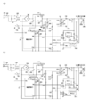
- the configuration shown in FIG. 5 (b) is an example.
- the configuration of FIG. 5B includes the input AC voltage correction circuit configured of the resistor 601 and the resistor 205 from the positive terminal of the primary smoothing capacitor 105, and the operation has been described above. It has the same effect as the overcurrent detection circuit.
- this input AC voltage correction circuit always consumes power by the combined resistance of the resistor 601 and the resistor 205 using the voltage at the positive terminal of the primary smoothing capacitor 105 as a power supply.
- FIG. 6 is a diagram showing a circuit diagram of a current resonant power supply device of the third embodiment. This embodiment is an example in which power saving is realized when the power switch is turned off, while providing the overcurrent detection circuit with the AC voltage correction function described in the first embodiment.
- 701 is a power switch
- 702 is a start resistance
- 703 is a transistor
- 704 is a photocoupler
- 705 is a control unit.
- the power supply switch 701 when the power supply switch 701 is turned on, the startup voltage is supplied to the VH terminal of the power supply control IC 110 through the startup resistor 702, and the power supply device starts up.
- the control unit 705 detects that the power switch 701 is turned off by means for detecting the on / off of the power switch (not shown).
- the control unit 705 operates the photocoupler 704 to shut off the power supply. With this configuration, even if the power switch 701 is suddenly turned off, the control unit 705 can decide to stop the power supply device. Therefore, various processes are performed when the power supply device is stopped. There is an advantage that it can be stopped.
- the power supply device shown in FIG. 6A if the power consumption when the power switch 701 is off can be suppressed, further power saving can be realized.
- the FET 106 when the power switch 701 is off, the FET 106 is off, so the input AC voltage correction circuit does not consume power as described in the first embodiment.
- the voltage between the drain and the source of the FET 107 can be used to correct the overcurrent detection circuit according to the input AC voltage.
- a configuration for performing input AC voltage correction can be considered.
- the configuration shown in FIG. 6 (b) is an example.
- the configuration of FIG. 6B there arises a problem that the power consumption is increased to provide the above-described function.
- the voltage at the positive terminal of the primary smoothing capacitor 105 is used as a power supply, and the voltage divided by the resistors 801 and 205 is used to input an AC to the overcurrent detection circuit. Voltage correction can be applied.
- the power switch is turned off, power is consumed by using the voltage at the positive terminal of the primary smoothing capacitor 105 as a power source by the resistors 801 and 205.
- the power supply device of the present embodiment shown in FIG. 6 it is possible to correct the input AC voltage while suppressing the power consumption when the power switch is off.
- the current resonant power supply described in the first to third embodiments can be applied, for example, as a low voltage power supply in an image forming apparatus such as a laser beam printer, a copying machine, and a facsimile.
- the present invention can be applied as power supply to a controller as a control unit in an image forming apparatus, or as a power supply for supplying power to motors as various drive units.
- the current resonant power supply described in the above embodiment is applicable not only to the image forming apparatus but also as a low voltage power supply in other electronic devices.
Landscapes
- Engineering & Computer Science (AREA)
- Power Engineering (AREA)
- Dc-Dc Converters (AREA)
Abstract
Description
前記1次巻線の他端と前記共振コンデンサとの間に接続され、前記トランスの1次側に流れる電流を検出する電流検出部と、前記1次巻線の一端と前記二つのスイッチング素子の間に接続され、前記トランスの1次側に入力される電圧の変化に応じて、前記電流検出部で検知した電流を補正する電流補正部とを有し、前記電流補正部からの出力に基づき前記電流共振電源を制御することを特徴とする。
まず、図7に示す回路図を用いて電流共振方式の電源装置(以下、電流共振電源装置という)の基本的な動作について説明する。図中の101はインレット、102はヒューズ、103はコモンモードコイル、104は整流ダイオードブリッジ、105は1次平滑コンデンサ、106と107はスイッチング素子としてのFETである。また、108は電流共振用のコンデンサ、109は電流検知用の抵抗、110は電源の動作を制御する制御IC、111は起動抵抗、112は抵抗、113はダイオード、114はコンデンサ、115はトランス、116はトランス115の1次巻線、117はトランス115の補助巻線、118と119はトランス115の2次巻線、120と121は整流ダイオード、122は平滑コンデンサ、123はフォトカプラ、124はシャントレギュレータ、125と126はレギュレーション抵抗、127は電圧出力部、128は電源装置に接続される負荷である。
1次平滑コンデンサ105→FET106→トランス115の1次巻線116→電流共振コンデンサ108→電流検出抵抗109→1次平滑コンデンサ105の経路で電流が流れる。
(状態2)FET106がオン→オフ状態でFET107がオフ状態
次に、FET106がオン状態からオフ状態になっても、トランス115の1次巻線116を流れる電流を維持しようと働くため、トランス115の1次巻線116→電流共振コンデンサ108→FET107に内蔵の寄生ダイオードの経路で電流が流れる。
(状態3)FET106がオフ状態でFET107がオフ→オン状態
次に、状態2の状態でFET107をオン状態にしても、引き続きトランス115の1次巻線116→電流共振コンデンサ108→FET107の経路で電流が流れる。ただし、トランス115の漏洩インダクタンスと電流共振コンデンサ108との共振作用により、次第に電流の流れは、電流共振コンデンサ108→トランス115の1次巻線116→FET107の経路に変化する。
(状態4)FET106がオフ状態でFET107がオフ状態
次に、状態3のまま、FET107をオフ状態にしても、トランス115の1次巻線116を流れる電流は維持しようと働き、トランス115の1次巻線116→FET106に内蔵の寄生ダイオード→1次平滑コンデンサ105の経路で電流が流れる。
(状態5)FET106がオフ→オン状態、FET107がオフ状態
Icd=(Ccd/(Ccd+Cr))×I ・・・ 式1
Cr:電流共振コンデンサ108の静電容量
Ccd:コンデンサ201の静電容量
そして、過電流検出回路として、入力AC電圧補正回路を無視し、電流検出回路だけの動作を考えた場合には、この電流Icdによって、抵抗205の両端に発生する電圧をVcdは、以下の式2で示される。
Vcd=Icd×Rcd ・・・ 式2
Rcd:抵抗205の抵抗値
(ただし、OCP端子以降の抵抗成分を無視した場合。)
なお、電流Iのピーク値をIpeakとした場合、Ipeakは以下の式3、式4、式5で表すことができる。
Ipeak=Vdch/X 式(3)
Vdch:Vdch:1次電解コンデンサ105の+端子電圧
X:トランス115の漏洩インダクタンスと電流共振コンデンサ108の合成リアクタンス
そして、
X=2×Π×f×Lr-1/(2×Π×f×Cr) ・・・ 式(4)
f:電源制御IC110で制御されるスイッチングFET106、107のスイッチング周波数
Lr:トランス115の漏洩インダクタンス
Cr:電流共振コンデンサ108の容量
つまり、
Ipeak
= Vdch/(2×Π×f×Lr-1/(2×Π×f×Cr))・・・式5
となる。
Vacr=((R205/(R205+R302))×Vdch×オン_DUTY)/(オン_DUTY+R/R205×オフ_DUTY)・・・式6
R205:抵抗205の抵抗値
R302:抵抗302の抵抗値
R:抵抗205と抵抗302の合成抵抗
Vdch:1次電解コンデンサ105の+端子電圧
オン_DUTY:スイッチングFET107がオン状態のときのDUTY比
オフ_DUTY:スイッチングFET107がオフ状態のときのDUTY比(ただし、 ダイオード301の順方向電圧は無視した場合。)
Vacr=((R205/(R205+R302))×Vdch×オン_DUTY)/(オン_DUTY+オフ_DUTY)・・・式7
Vocp≒Vcd+Vacr ・・・式8
・波形401
入力AC電圧が高く、入力AC電圧補正回路有りの場合のVocpの波形である。
・波形402
入力AC電圧が高く、入力AC電圧補正回路無しの場合のVocpの波形である。
・波形403
入力AC電圧が低く、入力AC電圧補正回路有りの場合のVocpの波形である。
・波形404
入力AC電圧が低く、入力AC電圧補正回路無しの場合のVocpの波形である。
波形401は、波形402に入力AC補正電圧が加算された波形となっている。この際の補正量は、入力AC電圧が高いため大きくなる。一方、波形403は、波形404に入力AC補正電圧が加算された波形となっている。この際の補正量は、入力AC電圧が低いため小さくなる。そして、入力AC補正電圧が加算された波形401と波形403の電圧は同じ値になる。このように、Vocpが入力AC電圧によらず一定になるようにすることで負荷128の電流が常に一定で過電流保護動作をかけることが可能となるのである。
上記の実施例1乃至実施例3で説明した電流共振電源を例えば、レーザビームプリンタ、複写機、ファクシミリ等の画像形成装置における低電圧電源として適用することができる。画像形成装置における制御部としてのコントローラへの電力供給、また、各種駆動部としてのモータに電力供給するための電源として適用可能である。
106、107 FET
108 電流共振コンデンサ
109 電流検知抵抗
110 電源制御IC
115 トランス
116 トランス115の1次巻線
117 トランス115の補助巻線
118、119 トランス115の2次巻き線
120、121 整流ダイオード
127 電圧出力部
128 負荷
201 電流検出コンデンサ
202、203、301 ダイオード
204 コンデンサ
205、302 抵抗
Claims (5)
- トランスと、前記トランスの1次巻線の一端と接続され、直列に配置された二つのスイッチング素子と、前記1次巻線の他端と接続された共振コンデンサと、前記二つのスイッチング素子を交互に動作することにより前記1次巻線と前記共振コンデンサを共振させて、前記トランスの2次巻線に交流電圧を誘起する電流共振電源であって、
前記1次巻線の他端と前記共振コンデンサとの間に接続され、前記トランスの1次側に流れる電流を検出する電流検出部と、
前記1次巻線の一端と前記二つのスイッチング素子の間に接続され、前記トランスの1次側に入力される電圧の変化に応じて、前記電流検出部で検知した電流を補正する電流補正部と、を有し、
前記電流補正部からの出力に基づき前記電流共振電源を制御する
ことを特徴とする電流共振電源。 - 前記二つのスイッチング素子の動作を制御する制御部を有し、
前記制御部は、前記電流補正部から出力される電流値が閾値以上である場合に、過電流であることを検出して前記二つのスイッチング素子の動作を停止することを特徴とする請求項1に記載の電流共振電源。 - 前記トランスは、前記制御部に電圧を供給するための補助巻線を有し、
前記2次巻線からの出力に応じて、前記補助巻線から前記制御部への電圧供給を制御する電圧供給制御部を有することを特徴とする請求項2に記載の電流共振電源。 - 前記トランスの1次側に入力される電圧の供給をオン・オフするスイッチを有し、
前記電圧供給制御部は、前記スイッチのオフに応じて前記補助巻線から前記制御部への電圧の供給をオフすることを特徴とする請求項3に記載の電流共振電源。 - 前記電流補正部は、前記1次巻線の一端と前記二つのスイッチング素子の間にダイオードと抵抗を接続した回路であることを特徴とする請求項1乃至4のいずれかの項に記載に電流共振電源。
Priority Applications (4)
| Application Number | Priority Date | Filing Date | Title |
|---|---|---|---|
| PCT/JP2010/057065 WO2011132275A1 (ja) | 2010-04-21 | 2010-04-21 | 電流共振電源 |
| CN201080066224.2A CN102859856B (zh) | 2010-04-21 | 2010-04-21 | 电流共振电源 |
| JP2012511450A JP5701292B2 (ja) | 2010-04-21 | 2010-04-21 | 電流共振電源 |
| US13/084,784 US8976545B2 (en) | 2010-04-21 | 2011-04-12 | Current resonance power supply for detecting overcurrent based on an output from a current compensation unit |
Applications Claiming Priority (1)
| Application Number | Priority Date | Filing Date | Title |
|---|---|---|---|
| PCT/JP2010/057065 WO2011132275A1 (ja) | 2010-04-21 | 2010-04-21 | 電流共振電源 |
Publications (1)
| Publication Number | Publication Date |
|---|---|
| WO2011132275A1 true WO2011132275A1 (ja) | 2011-10-27 |
Family
ID=44815686
Family Applications (1)
| Application Number | Title | Priority Date | Filing Date |
|---|---|---|---|
| PCT/JP2010/057065 Ceased WO2011132275A1 (ja) | 2010-04-21 | 2010-04-21 | 電流共振電源 |
Country Status (4)
| Country | Link |
|---|---|
| US (1) | US8976545B2 (ja) |
| JP (1) | JP5701292B2 (ja) |
| CN (1) | CN102859856B (ja) |
| WO (1) | WO2011132275A1 (ja) |
Cited By (4)
| Publication number | Priority date | Publication date | Assignee | Title |
|---|---|---|---|---|
| JP2013099110A (ja) * | 2011-10-31 | 2013-05-20 | Canon Inc | 電源装置および画像形成装置 |
| JP2015019534A (ja) * | 2013-07-12 | 2015-01-29 | キヤノン株式会社 | 電源装置及び画像形成装置 |
| US10236680B2 (en) | 2016-08-30 | 2019-03-19 | Fuji Electric Co., Ltd. | Control circuit of switching power supply device |
| US12445057B2 (en) | 2022-08-10 | 2025-10-14 | Fuji Electric Co., Ltd. | Switching control circuit and power supply circuit |
Families Citing this family (8)
| Publication number | Priority date | Publication date | Assignee | Title |
|---|---|---|---|---|
| US8842449B1 (en) * | 2013-03-12 | 2014-09-23 | XP Power Limited | LLC resonant converter with lossless primary-side current feedback |
| US11083067B2 (en) * | 2013-03-15 | 2021-08-03 | Hatch Transformers, Inc. | Electrical power supply with removable plug-in cartridge |
| KR101949954B1 (ko) | 2013-06-07 | 2019-02-19 | 삼성전자주식회사 | 고효율 에너지 주입을 위한 무선 전력 전송 장치 |
| JP6007935B2 (ja) * | 2014-03-26 | 2016-10-19 | サンケン電気株式会社 | 電流共振型電源装置 |
| WO2016026090A1 (en) * | 2014-08-19 | 2016-02-25 | Abbeydorney Holdings Ltd. | Driving circuit, lighting device and method of reducing power dissipation |
| JP7114364B2 (ja) * | 2018-06-22 | 2022-08-08 | キヤノン株式会社 | 電源装置及び画像形成装置 |
| JP7061548B2 (ja) * | 2018-10-04 | 2022-04-28 | 株式会社日立産機システム | 共振型電源装置 |
| CN111987695B (zh) * | 2020-07-27 | 2022-11-04 | 株洲麦格米特电气有限责任公司 | 一种谐振变换器、谐振变换器的过流保护方法及电子设备 |
Citations (6)
| Publication number | Priority date | Publication date | Assignee | Title |
|---|---|---|---|---|
| JPH0497480U (ja) * | 1991-01-17 | 1992-08-24 | ||
| JPH0622467A (ja) * | 1992-06-30 | 1994-01-28 | Sony Corp | 充電装置 |
| JPH07274499A (ja) * | 1994-03-24 | 1995-10-20 | Sanken Electric Co Ltd | スイッチング電源装置 |
| JPH08111977A (ja) * | 1994-10-12 | 1996-04-30 | Sanken Electric Co Ltd | スイッチング電源装置 |
| JP2002142456A (ja) * | 2000-10-30 | 2002-05-17 | Oki Electric Ind Co Ltd | 直流電源装置 |
| JP2009261100A (ja) * | 2008-04-15 | 2009-11-05 | Mitsubishi Electric Corp | スイッチング電源の過電流保護回路 |
Family Cites Families (16)
| Publication number | Priority date | Publication date | Assignee | Title |
|---|---|---|---|---|
| US4400644A (en) | 1981-04-29 | 1983-08-23 | Rca Corporation | Self-indexing insulating support rods for an electron gun assembly |
| US5333104A (en) * | 1992-05-22 | 1994-07-26 | Matsushita Electric Works, Ltd. | Inverter power source |
| KR100219314B1 (ko) * | 1992-09-25 | 1999-09-01 | 무라따 미치히로 | 공진형 전원 회로 |
| DE60114794T2 (de) * | 2000-04-10 | 2006-07-20 | Koninklijke Philips Electronics N.V. | Evg mit spitzendetektion |
| US6836415B1 (en) * | 2003-06-18 | 2004-12-28 | Systems General Corp. | Primary-side regulated pulse width modulation controller with improved load regulation |
| US6940189B2 (en) * | 2003-07-31 | 2005-09-06 | Andrew Roman Gizara | System and method for integrating a digital core with a switch mode power supply |
| JP4029853B2 (ja) * | 2004-03-23 | 2008-01-09 | サンケン電気株式会社 | スイッチング電源装置 |
| EP1869759B1 (en) * | 2005-04-01 | 2019-08-07 | Nxp B.V. | Control of a resonant converter |
| JP4797637B2 (ja) * | 2006-01-16 | 2011-10-19 | サンケン電気株式会社 | 共振型スイッチング電源装置 |
| JP4720514B2 (ja) * | 2006-01-17 | 2011-07-13 | 富士電機システムズ株式会社 | 共振コンバータにおける電流検出方式 |
| TWM305504U (en) * | 2006-08-28 | 2007-01-21 | Hipro Electronics Taiwan Co Lt | Voltage stabilization circuit for forward-type transformer |
| US7848117B2 (en) * | 2007-01-22 | 2010-12-07 | Power Integrations, Inc. | Control arrangement for a resonant mode power converter |
| JP2008283787A (ja) * | 2007-05-10 | 2008-11-20 | Matsushita Electric Ind Co Ltd | スイッチング電源装置 |
| KR101471133B1 (ko) * | 2008-01-31 | 2014-12-09 | 페어차일드코리아반도체 주식회사 | 공진형 컨버터 |
| US7742318B2 (en) * | 2008-06-10 | 2010-06-22 | Virginia Tech Intellectual Properties, Inc. | Multi-element resonant converters |
| JP4548532B2 (ja) * | 2008-08-29 | 2010-09-22 | ブラザー工業株式会社 | 電源装置および当該装置を備えた画像形成装置 |
-
2010
- 2010-04-21 WO PCT/JP2010/057065 patent/WO2011132275A1/ja not_active Ceased
- 2010-04-21 CN CN201080066224.2A patent/CN102859856B/zh active Active
- 2010-04-21 JP JP2012511450A patent/JP5701292B2/ja active Active
-
2011
- 2011-04-12 US US13/084,784 patent/US8976545B2/en active Active
Patent Citations (6)
| Publication number | Priority date | Publication date | Assignee | Title |
|---|---|---|---|---|
| JPH0497480U (ja) * | 1991-01-17 | 1992-08-24 | ||
| JPH0622467A (ja) * | 1992-06-30 | 1994-01-28 | Sony Corp | 充電装置 |
| JPH07274499A (ja) * | 1994-03-24 | 1995-10-20 | Sanken Electric Co Ltd | スイッチング電源装置 |
| JPH08111977A (ja) * | 1994-10-12 | 1996-04-30 | Sanken Electric Co Ltd | スイッチング電源装置 |
| JP2002142456A (ja) * | 2000-10-30 | 2002-05-17 | Oki Electric Ind Co Ltd | 直流電源装置 |
| JP2009261100A (ja) * | 2008-04-15 | 2009-11-05 | Mitsubishi Electric Corp | スイッチング電源の過電流保護回路 |
Cited By (5)
| Publication number | Priority date | Publication date | Assignee | Title |
|---|---|---|---|---|
| JP2013099110A (ja) * | 2011-10-31 | 2013-05-20 | Canon Inc | 電源装置および画像形成装置 |
| JP2015019534A (ja) * | 2013-07-12 | 2015-01-29 | キヤノン株式会社 | 電源装置及び画像形成装置 |
| US9274490B2 (en) | 2013-07-12 | 2016-03-01 | Canon Kabushiki Kaisha | Power supply apparatus and image forming apparatus |
| US10236680B2 (en) | 2016-08-30 | 2019-03-19 | Fuji Electric Co., Ltd. | Control circuit of switching power supply device |
| US12445057B2 (en) | 2022-08-10 | 2025-10-14 | Fuji Electric Co., Ltd. | Switching control circuit and power supply circuit |
Also Published As
| Publication number | Publication date |
|---|---|
| JP5701292B2 (ja) | 2015-04-15 |
| CN102859856B (zh) | 2016-09-14 |
| US20110261592A1 (en) | 2011-10-27 |
| US8976545B2 (en) | 2015-03-10 |
| JPWO2011132275A1 (ja) | 2013-07-18 |
| CN102859856A (zh) | 2013-01-02 |
Similar Documents
| Publication | Publication Date | Title |
|---|---|---|
| JP5701292B2 (ja) | 電流共振電源 | |
| JP6218467B2 (ja) | 電源装置及び画像形成装置 | |
| US8009447B2 (en) | Energy effective switching power supply apparatus and an energy effective method thereof | |
| JP6433652B2 (ja) | 電源装置及び電気機器 | |
| US20100315841A1 (en) | Semiconductor device and switching power supply apparatus | |
| KR101889108B1 (ko) | 대기전력소모를 감소시키는 전력변환장치 | |
| US20100020575A1 (en) | Switching power supply device | |
| JP5117980B2 (ja) | エネルギー伝達装置およびエネルギー伝達制御用半導体装置 | |
| JP5693048B2 (ja) | 電流共振電源 | |
| JP2004201385A (ja) | Dc/dcコンバータ回路 | |
| JP2016144310A (ja) | スイッチング電源装置 | |
| JP2010273431A (ja) | 力率改善型スイッチング電源装置 | |
| JP2005245142A (ja) | スイッチング電源制御用半導体装置 | |
| JP5277706B2 (ja) | スイッチング電源装置 | |
| JP2004328837A (ja) | スイッチング電源回路およびこれを備えたスイッチングレギュレータ | |
| JP4650101B2 (ja) | スイッチング電源装置、及びオーディオアンプシステム | |
| JP2024176551A (ja) | 電源装置 | |
| JP2008263728A (ja) | 電源装置 | |
| JP5130936B2 (ja) | 直流‐直流変換装置 | |
| JP2008067580A (ja) | スイッチング電源装置 | |
| KR100629518B1 (ko) | 다출력 스위칭 전원장치 | |
| JP2005080486A (ja) | スイッチング電源装置 | |
| JP2011254640A (ja) | 絶縁型スイッチング電源 | |
| JP2009201330A (ja) | スイッチング電源回路 | |
| KR20060086596A (ko) | 크로스 레귤레이션을 보상하는 회로를 갖는 스위칭 전원장치 |
Legal Events
| Date | Code | Title | Description |
|---|---|---|---|
| WWE | Wipo information: entry into national phase |
Ref document number: 201080066224.2 Country of ref document: CN |
|
| 121 | Ep: the epo has been informed by wipo that ep was designated in this application |
Ref document number: 10850218 Country of ref document: EP Kind code of ref document: A1 |
|
| WWE | Wipo information: entry into national phase |
Ref document number: 2012511450 Country of ref document: JP |
|
| NENP | Non-entry into the national phase |
Ref country code: DE |
|
| 122 | Ep: pct application non-entry in european phase |
Ref document number: 10850218 Country of ref document: EP Kind code of ref document: A1 |