WO2011129299A1 - プリント配線板およびその製造方法 - Google Patents
プリント配線板およびその製造方法 Download PDFInfo
- Publication number
- WO2011129299A1 WO2011129299A1 PCT/JP2011/059001 JP2011059001W WO2011129299A1 WO 2011129299 A1 WO2011129299 A1 WO 2011129299A1 JP 2011059001 W JP2011059001 W JP 2011059001W WO 2011129299 A1 WO2011129299 A1 WO 2011129299A1
- Authority
- WO
- WIPO (PCT)
- Prior art keywords
- printed wiring
- electromagnetic wave
- wave shielding
- wiring board
- film
- Prior art date
- Legal status (The legal status is an assumption and is not a legal conclusion. Google has not performed a legal analysis and makes no representation as to the accuracy of the status listed.)
- Ceased
Links
Images


Classifications
-
- H—ELECTRICITY
- H05—ELECTRIC TECHNIQUES NOT OTHERWISE PROVIDED FOR
- H05K—PRINTED CIRCUITS; CASINGS OR CONSTRUCTIONAL DETAILS OF ELECTRIC APPARATUS; MANUFACTURE OF ASSEMBLAGES OF ELECTRICAL COMPONENTS
- H05K1/00—Printed circuits
- H05K1/02—Details
- H05K1/0213—Electrical arrangements not otherwise provided for
- H05K1/0216—Reduction of cross-talk, noise or electromagnetic interference
- H05K1/0218—Reduction of cross-talk, noise or electromagnetic interference by printed shielding conductors, ground planes or power plane
-
- H—ELECTRICITY
- H05—ELECTRIC TECHNIQUES NOT OTHERWISE PROVIDED FOR
- H05K—PRINTED CIRCUITS; CASINGS OR CONSTRUCTIONAL DETAILS OF ELECTRIC APPARATUS; MANUFACTURE OF ASSEMBLAGES OF ELECTRICAL COMPONENTS
- H05K1/00—Printed circuits
- H05K1/02—Details
- H05K1/0213—Electrical arrangements not otherwise provided for
- H05K1/0237—High frequency adaptations
- H05K1/0242—Structural details of individual signal conductors, e.g. related to the skin effect
-
- H—ELECTRICITY
- H05—ELECTRIC TECHNIQUES NOT OTHERWISE PROVIDED FOR
- H05K—PRINTED CIRCUITS; CASINGS OR CONSTRUCTIONAL DETAILS OF ELECTRIC APPARATUS; MANUFACTURE OF ASSEMBLAGES OF ELECTRICAL COMPONENTS
- H05K1/00—Printed circuits
- H05K1/02—Details
- H05K1/0213—Electrical arrangements not otherwise provided for
- H05K1/0216—Reduction of cross-talk, noise or electromagnetic interference
- H05K1/023—Reduction of cross-talk, noise or electromagnetic interference using auxiliary mounted passive components or auxiliary substances
- H05K1/0234—Resistors or by disposing resistive or lossy substances in or near power planes
-
- H—ELECTRICITY
- H05—ELECTRIC TECHNIQUES NOT OTHERWISE PROVIDED FOR
- H05K—PRINTED CIRCUITS; CASINGS OR CONSTRUCTIONAL DETAILS OF ELECTRIC APPARATUS; MANUFACTURE OF ASSEMBLAGES OF ELECTRICAL COMPONENTS
- H05K1/00—Printed circuits
- H05K1/02—Details
- H05K1/03—Use of materials for the substrate
- H05K1/0393—Flexible materials
-
- H—ELECTRICITY
- H05—ELECTRIC TECHNIQUES NOT OTHERWISE PROVIDED FOR
- H05K—PRINTED CIRCUITS; CASINGS OR CONSTRUCTIONAL DETAILS OF ELECTRIC APPARATUS; MANUFACTURE OF ASSEMBLAGES OF ELECTRICAL COMPONENTS
- H05K2201/00—Indexing scheme relating to printed circuits covered by H05K1/00
- H05K2201/01—Dielectrics
- H05K2201/0104—Properties and characteristics in general
- H05K2201/0133—Elastomeric or compliant polymer
-
- H—ELECTRICITY
- H05—ELECTRIC TECHNIQUES NOT OTHERWISE PROVIDED FOR
- H05K—PRINTED CIRCUITS; CASINGS OR CONSTRUCTIONAL DETAILS OF ELECTRIC APPARATUS; MANUFACTURE OF ASSEMBLAGES OF ELECTRICAL COMPONENTS
- H05K2201/00—Indexing scheme relating to printed circuits covered by H05K1/00
- H05K2201/07—Electric details
- H05K2201/0707—Shielding
- H05K2201/0715—Shielding provided by an outer layer of PCB
-
- H—ELECTRICITY
- H05—ELECTRIC TECHNIQUES NOT OTHERWISE PROVIDED FOR
- H05K—PRINTED CIRCUITS; CASINGS OR CONSTRUCTIONAL DETAILS OF ELECTRIC APPARATUS; MANUFACTURE OF ASSEMBLAGES OF ELECTRICAL COMPONENTS
- H05K2201/00—Indexing scheme relating to printed circuits covered by H05K1/00
- H05K2201/09—Shape and layout
- H05K2201/09209—Shape and layout details of conductors
- H05K2201/09654—Shape and layout details of conductors covering at least two types of conductors provided for in H05K2201/09218 - H05K2201/095
- H05K2201/09736—Varying thickness of a single conductor; Conductors in the same plane having different thicknesses
Definitions
- the present invention relates to a printed wiring board with an electromagnetic wave shielding function and a method for manufacturing the same.
- EMI noise generated from printed wiring boards, electronic parts, etc. affects other electric circuits and electronic parts and may cause malfunctions, so it is necessary to shield the electromagnetic noise. Therefore, an electromagnetic wave shielding function is imparted to the printed wiring board.
- the space allowed for the printed wiring board is becoming narrower. Therefore, the printed wiring board is required to be thin, and the flexible printed wiring board is required to reduce the bending radius. In various usage environments, the wiring function can be achieved without losing the reliability of the electromagnetic shielding function. It is demanded.
- An undercoat layer, a shield layer coated with a conductive paste containing metal powder, and an overcoat layer are sequentially provided on the copper foil wiring circuit on the surface of the heat-resistant plastic film, and a ground pattern of the copper foil wiring circuit and the shield layer are provided.
- a flexible printed wiring board that is electrically connected through the undercoat layer at an appropriate interval Patent Document 1.
- An insulating layer is provided that insulates an electromagnetic wave shielding film in which a metal thin film layer and a conductive adhesive layer containing a metal filler are sequentially provided on one side of the coverlay film except for a part of the ground circuit in the printed circuit.
- a flexible printed wiring board (Patent Document 2) in which the conductive adhesive layer is placed on the base film so as to adhere to the insulating layer and a part of the ground circuit.
- the flexible printed wiring board (1) has the following problems.
- the shield layer containing metal powder is brittle because it has many different material interfaces, and does not have sufficient strength against repeated bending of the flexible wiring board.
- An undercoat layer is required to maintain insulation between the copper foil wiring circuit excluding a part of the ground pattern and the shield layer, and the flexible printed wiring board becomes thick.
- In order to electrically connect a part of the ground pattern and the shield layer it is necessary to form a through hole in a part of the undercoat layer, and it takes time to process the through hole.
- the shield layer Since the shield layer is exposed on the peripheral end face of the flexible printed wiring board, it is corroded by moisture ingress or contact with oxygen, and the resistance value increases, and the electromagnetic wave shielding function is reduced. That is, the reliability of the electromagnetic wave shielding function is low.
- the shield layer Since the shield layer is made of a cured resin obtained by curing the conductive paste, the shield layer cannot be etched into a desired shape using an etchant.
- the flexible printed wiring board (2) has the following problems.
- the conductive adhesive layer containing a metal filler is brittle because it has many different material interfaces, and does not have sufficient strength against repeated bending of the flexible wiring board.
- An insulating layer is required to maintain insulation between the printed circuit excluding a part of the ground circuit and the conductive adhesive layer, and the flexible printed wiring board becomes thick.
- In order to electrically connect a part of the ground circuit and the conductive adhesive layer it is necessary to form a through hole in a part of the insulating layer, and it takes time to process the through hole.
- the present invention has been made in view of the above circumstances, has an electromagnetic wave shielding function without connecting the electromagnetic wave shielding layer to the ground, has high reliability, and has excellent flexibility in a flexible printed wiring board.
- a printed wiring board that can be thinned and that can etch an electromagnetic wave shielding layer and a conductor with the same etchant and a method for manufacturing the same are provided.
- a first aspect of the present invention is a printed wiring member having a target conductor to be subjected to electromagnetic wave shielding on at least one surface of an insulating layer, and a low resistance portion and a high resistance on at least one surface of a base film.
- An electromagnetic shielding member having an electromagnetic shielding layer composed of a resistance portion; and the printed wiring member and the electromagnetic shielding member are arranged to face each other with the electromagnetic shielding layer spaced apart so as to cover the target conductor.
- a printed wiring board bonded through an insulating adhesive layer; the electromagnetic shielding layer and the target conductor are made of the same kind of conductive material; and the electromagnetic shielding layer is a peripheral edge of the printed wiring board. It is a printed wiring board which is not exposed to the end face.
- a second aspect of the present invention is the printed wiring board according to the first aspect, wherein the electromagnetic wave shielding layer is separated from a via hole or a through hole of the printed wiring board.
- the low resistance portion has a surface resistance of 0.01 to 5 ⁇
- the high resistance portion has a surface resistance of the low resistance portion.
- a fourth aspect of the present invention is the printed wiring board according to any one of the first to third aspects, wherein the high resistance portion is repeatedly formed at intervals.
- a fifth aspect of the present invention is the base film according to any one of the first to fourth aspects, wherein the base film is formed on a part of at least one surface of the base film.
- the electromagnetic wave shielding layer is a deposited film made of a conductive material formed on the surface of the base film on the side where the soft material portion is formed;
- the vapor-deposited film formed on the surface of the material film is a low-resistance portion, and the vapor-deposited film formed on the surface of the soft material portion is a printed wiring board that becomes the high-resistance portion.
- the base film is a concavo-convex portion formed on a part of at least one surface of the base film, and the concavo-convex portion.
- the electromagnetic wave shielding layer is a deposited film made of a conductive material formed on the surface of the base film on the side where the uneven portion is formed; formed on the non-recessed portion The deposited film thus formed serves as a low resistance portion, and the deposited film formed on the concavo-convex portion serves as a high resistance portion.
- a printed wiring board manufacturing method including the following steps (I) to (III): is there.
- (I) A step of etching the conductor of the printed wiring member into a desired shape using an etching solution.
- the electromagnetic wave shielding layer of the electromagnetic wave shielding member is formed in a desired shape, and the electromagnetic wave shielding layer is printed wiring in the printed wiring board obtained in the following step (III). Etching to a size that does not expose the peripheral edge of the plate.
- the printed wiring member and the electromagnetic wave shielding member are disposed opposite to each other so as to cover the target conductor and bonded via an insulating adhesive layer, and then trimming of the outer shape is performed. Process.
- the printed wiring board of the present invention has an electromagnetic wave shielding function without connecting the electromagnetic wave shielding layer to the ground, has high reliability, and is flexible in a flexible printed wiring board and can be thinned.
- the electromagnetic wave shielding layer and the conductor can be etched with the same etching solution during production.
- an electromagnetic wave shielding function is provided without connecting the electromagnetic wave shielding layer to the ground, the reliability is high, and the flexible printed wiring board is excellent in flexibility and thin.
- the printed wiring board can be manufactured, and the same etching solution can be used when etching the electromagnetic wave shielding layer and the conductor.
- FIG. 1 is a cross-sectional view showing an example of the printed wiring board of the present invention.
- the printed wiring board 1 includes an electromagnetic wave shielding member 10 having an electromagnetic wave shielding layer 22 composed of a low resistance portion 22a and a high resistance portion 22b on one surface of a base film 20, and an insulating property on both surfaces of the electromagnetic wave shielding member 10.
- a printed wiring member 41 having a conductor 46 is provided on one surface of the layer 42.
- the electromagnetic wave shielding layer 22 is disposed so as to face the target conductor 44 while being spaced apart via the insulating adhesive layer 30. Further, the electromagnetic wave shielding layer 22 is not formed on the peripheral edge portion 14 of the electromagnetic wave shielding member 10, and thus the electromagnetic wave shielding layer 22 is not exposed on the peripheral edge surface of the printed wiring board 1. In addition, the electromagnetic shielding layer 22 is not formed in the peripheral portion 16 of the via hole 48, and thus the electromagnetic shielding layer 22 is separated from the via hole 48.
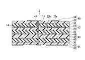
- FIG. 2 is a cross-sectional view showing another example of the printed wiring board of the present invention.
- the printed wiring board 2 has an electromagnetic wave shielding member 12 having an electromagnetic wave shielding layer 22 composed of a low resistance portion 22a and a high resistance portion 22b on one surface of the base film 20, and on one surface of the electromagnetic wave shielding member 12, A printed wiring member 40 having a target conductor 44 to be subjected to electromagnetic wave shielding on one surface of the insulating layer 42 bonded through the insulating adhesive layer 30; and the other surface of the electromagnetic wave shielding member 12
- a target conductor 44 to be subjected to electromagnetic wave shielding is provided on one surface of the insulating layer 42 bonded through the insulating adhesive layer 30, and a conductor is provided on the other surface of the insulating layer 42.
- the electromagnetic wave shielding layer 22 is disposed so as to face the target conductor 44 while being spaced apart via the insulating adhesive layer 30. Further, the electromagnetic wave shielding layer 22 is not formed on the peripheral edge portion 14 of the electromagnetic wave shielding member 12, and thus the electromagnetic wave shielding layer 22 is not exposed on the peripheral edge surface of the printed wiring board 2. In addition, the electromagnetic shielding layer 22 is not formed in the peripheral portion 16 of the via hole 48, and thus the electromagnetic shielding layer 22 is separated from the via hole 48.
- the electromagnetic wave shielding member examples include the following two types of members.
- the base film has a concavo-convex portion formed on a part of at least one surface of the base film and a non-concave portion excluding the concavo-convex portion; an electromagnetic wave shielding layer is formed with the concavo-convex portion.
- the electromagnetic wave shielding film which is a vapor deposition film which consists of an electroconductive material formed in the surface of the base film of the other side.
- the base film has a soft material portion that is formed on a part of at least one surface of the base film and is softer than the surface of the base film; the electromagnetic wave shielding layer is the soft material.
- the electromagnetic wave shielding film which is a vapor deposition film which consists of an electroconductive material formed in the surface of the base film of the side in which the part was formed.
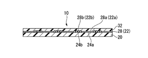
- FIG. 3 is a cross-sectional view showing an example of the electromagnetic wave shielding film ( ⁇ ).
- the electromagnetic wave shielding member 10 has a printed part (uneven portion 24b) formed by printing on a part of one side of the substrate film 20, and a non-printed portion (non-uneven portion 24a) excluding the printed portion.
- a vapor-deposited film 28 that is, an electromagnetic wave shielding layer 22
- a protective layer 32 that protects the surface of the vapor-deposited film
- FIG. 4 is a cross-sectional view showing another example of the electromagnetic wave shielding film ( ⁇ ).
- the electromagnetic wave shielding member 11 includes a roughened portion (uneven portion 24b) formed by roughening a part of one surface of the base film 20, and a non-roughened portion (non-uneven portion 24a) excluding the roughened portion.
- a deposited film 28 that is, the electromagnetic wave shielding layer 22 made of a conductive material formed on the surface of the substrate film 20 on the side where the roughened portion is formed.
- the deposited film 28a formed on the non-concave portion 24a becomes the low resistance portion 22a
- the deposited film 28b formed on the uneven portion 24b becomes the high resistance portion 22b. That is, the surface resistance of the vapor deposition film 28 differs between the vapor deposition film 28 a formed on the non-concave portion 24 a of the base film 20 and the vapor deposition film 28 b formed on the concave portion 24 b of the base film 20.
- the unevenness portion 24b of the base film 20 has a larger area in consideration of actual unevenness than the projected area when viewed from the upper surface in the direction orthogonal to the surface of the base film 20.
- the vapor deposition film 28b formed on the uneven portion 24b of the base film 20 becomes thinner than the vapor deposition film 28a formed on the non-concave portion 24a.
- the surface resistance of the vapor deposition film 28b becomes larger than the surface resistance of the vapor deposition film 28a.
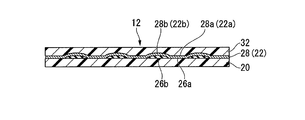
- FIG. 5 is a cross-sectional view showing an example of the electromagnetic wave shielding film ( ⁇ ).
- the electromagnetic wave shielding member 12 is formed by printing on a part of one side of the base film 20, and is softer than the surface of the base film 20, and the base film excluding the soft material part 26b.
- a protective layer 32 for protecting the surface of 28. The protective layer 32 is removed when the printed wiring member is bonded to the surface on the vapor deposition film 28 side via the insulating adhesive layer 30.
- the vapor deposition film 28a formed on the surface 26a of the base film 20 becomes the low resistance portion 22a, and the vapor deposition film 28b formed on the surface of the soft material portion 26b becomes the high resistance portion 22b. It becomes. That is, the surface resistance of the vapor deposition film 28 differs between the vapor deposition film 28 a formed on the surface 26 a of the base film 20 and the vapor deposition film 28 b formed on the soft material portion 26 b of the base film 20.
- a metal is vapor-deposited on the surface 26a of the relatively hard base film 20 first, a plurality of atoms are condensed to form islands, the islands gradually grow and the islands merge to form a continuous vapor deposition film.
- the base film 20 is a film that serves as a base when the uneven portion 24b or the soft material portion 26b and the vapor deposition film 28 are formed.
- Examples of the material of the base film 20 include a resin or a rubber elastic body.
- Examples of the resin include polyimide, liquid crystal polymer, polyaramid, polyphenylene sulfide, polyamideimide, polyetherimide, polyethylene naphthalate, and polyethylene terephthalate.
- the surface hardness (Vickers hardness) of the base film 20 is preferably 400 or more from the viewpoint of forming the vapor deposition film 28a to be the low resistance portion 22a. Moreover, the surface hardness (Vickers hardness) of the base film 20 is preferably 1200 or less from the viewpoint of flexibility. The surface resistance of the base film 20 is preferably 1 ⁇ 10 6 ⁇ or more. The thickness of the base film 20 is preferably 3 to 25 ⁇ m from the viewpoint of flexibility. When the base film 20 is thin, handling during processing becomes difficult. Therefore, a reinforcing material such as a slightly adhesive sheet may be temporarily attached.
- the concavo-convex portion 24 b can be formed by performing printing, roughening treatment, etching treatment, or the like on the surface of the base film 20.
- Examples of printing include gravure printing and flexographic printing.
- the printing ink used for printing preferably contains an anti-blocking agent (for example, polymer particles or the like) from the viewpoint of easily forming irregularities in the printing part.
- Examples of the surface roughening treatment include blast treatment.
- the material of the base film 20 is polyimide, it can be roughened by alkali treatment or the like.
- Examples of the etching treatment include wet etching, dry etching (laser etching, etc.) and the like.
- the arithmetic average roughness Ra of the uneven part 24b is preferably 0.3 to 3 ⁇ m.
- the arithmetic average roughness Ra of the concavo-convex portion 24b is 0.3 ⁇ m or more, the vapor deposition film 28b formed on the concavo-convex portion 24b is sufficiently thin, and the surface resistance of the vapor deposition film 28b is sufficiently high. If the arithmetic average roughness Ra of the uneven part 24b is 3 ⁇ m or less, the strength reduction of the base film 20 is suppressed.
- the arithmetic average roughness Ra is an arithmetic average roughness according to JIS B0651: 1996.
- Examples of the shape of the region where the uneven portion 24b is formed include a rod shape, a circular shape, a key shape, and a spiral shape.
- the maximum length per one concavo-convex portion 24b is preferably 1 ⁇ 4 or less of the wavelength ⁇ of electromagnetic wave noise shielded by the vapor deposition film 28.
- the area per concavo-convex portion 24 b is preferably 0.1 to 40 mm 2 and more preferably 0.25 to 20 mm 2 from the viewpoint of the electromagnetic wave shielding function by the deposited film 28.
- the concavo-convex portions 24b are repeatedly formed at a predetermined pitch over the entire surface of the base film 20 so that the vapor deposition film 28 can shield electromagnetic wave noise evenly.
- the total area of the concavo-convex portions 24b is preferably 10 to 50% of the area (100%) of the deposited film 28.
- the total area of the concavo-convex portions 24b is less than 10%, sufficient loss of the high-frequency current flowing through the vapor deposition film 28 cannot be achieved by the vapor deposition film 28b serving as the high resistance portion 22b.
- the total area of the concavo-convex portions 24b exceeds 50%, it is necessary to increase the thickness of the deposited film 28 in order to maintain the electromagnetic wave shielding function.
- the non-concave portions 24a are surfaces that are not actively printed, roughened, etched, or the like.
- the non-concave portion 24a may have some unevenness as long as the arithmetic average roughness Ra is sufficiently smaller than the uneven portion 24b.
- the arithmetic average roughness Ra of the non-concave portion 24a is preferably 0.1 ⁇ m or less.
- the deposited film 28 formed on the non-recessed portion 24a becomes thick, and the surface resistance of the deposited film 28a that becomes the low resistance portion 22a is sufficiently high. Lower.
- the soft material portion 26b is made of a soft material.
- the soft material is a material softer than the material constituting the surface 26a of the base film 20, and specifically, a material having a hardness (Vickers hardness) lower than that of the surface 26a of the base film 20. is there.
- the hardness (Vickers hardness) of the soft material portion 26b is preferably 500 or less from the viewpoint of forming the vapor deposition film 28b to be the high resistance portion 22b.
- the hardness (Vickers hardness) of the soft material portion 26b is preferably 150 or more from the viewpoint of shape maintenance.
- a soft material portion formed by printing using soft ink As the soft material portion 26b, a soft material portion formed by printing using soft ink; a soft material portion formed by printing using ink containing soft fillers such as particles such as elastic bodies having a small particle diameter and powder Etc. From the viewpoint of easy formation, a soft material portion formed by printing using soft ink is preferable.
- the printing method include a gravure printing method and a screen printing method.
- the soft ink include a soft ink using a urethane resin, a polyester resin, a polyamide resin, an epoxy resin, a synthetic rubber, or the like as a binder.
- Examples of the shape of the soft material portion 26b include a rod shape, a circular shape, a key shape, and a spiral shape.
- the maximum length per soft material portion 26b is preferably equal to or less than 1 ⁇ 4 of the wavelength ⁇ of electromagnetic wave noise shielded by the deposited film 28.
- the area per soft material portion 26b is preferably 0.1 to 40 mm 2 and more preferably 0.25 to 20 mm 2 from the viewpoint of the electromagnetic wave shielding function by the deposited film 28.
- the soft material portion 26b is preferably formed repeatedly at a predetermined pitch over the entire surface of the base film 20 so that the vapor deposition film 28 can shield electromagnetic wave noise evenly.
- the total area of the soft material portion 26b is preferably 10 to 50% of the area (100%) of the deposited film 28. If the total area of the soft material portion 26b is less than 10%, sufficient loss of high-frequency current flowing through the vapor deposition film 28 cannot be achieved by the vapor deposition film 28b serving as the high resistance portion 22b. If the total area of the soft material portion 26b exceeds 50%, it is necessary to make the vapor deposition film 28 thick in order to maintain the electromagnetic wave shielding function.
- the vapor deposition film 28 is a film made of a conductive material formed by physically vapor-depositing a conductive material on the surface of the base film 20 and the surface of the uneven portion 24b or the soft material portion 26b.
- the conductive material is the same type of conductive material as that of the conductor of the printed wiring member.
- the “same kind of conductive material” means that the main components are the same, and the material can be etched using the same etchant as the etchant used for etching the conductor.
- Examples of the conductive material include metals and conductive ceramics. As the metal, gold, silver, copper, aluminum, or nickel is preferable, and copper is particularly preferable.
- conductive ceramics may be used from the viewpoint of improving environmental resistance.
- the conductive ceramic include an alloy, an intermetallic compound, a solid solution, and the like including a metal and one or more elements selected from the group consisting of boron, carbon, nitrogen, silicon, phosphorus, and sulfur.
- nickel nitride, titanium nitride, tantalum nitride, chromium nitride, titanium carbide, silicon carbide, chromium carbide, vanadium carbide, zirconium carbide, molybdenum carbide, tungsten carbide, chromium boride, molybdenum boride, chromium silicide Examples thereof include zirconium silicide.
- Examples of physical vapor deposition include EB vapor deposition, ion beam vapor deposition, and sputtering, and physical vapor deposition may be performed under gas flow for ceramicization.
- the surface resistance of the deposited film 28a (low resistance portion 22a) is preferably 0.01 to 5 ⁇ , more preferably 0.01 to 1 ⁇ , from the viewpoint of an electromagnetic wave shielding function for reflecting electromagnetic waves.
- the surface resistance of the deposited film 28b (high resistance portion 22b) is preferably 2 to 100 times the surface resistance of the deposited film 28a from the viewpoint of sufficiently losing the high-frequency current flowing through the deposited film 28.
- the thickness of the vapor deposition film 28 is preferably 50 to 200 nm from the viewpoint of bending resistance.
- the transmission attenuation characteristic of the deposited film 28 is preferably ⁇ 10 dB or less, and more preferably ⁇ 20 dB or less.
- the transmission attenuation characteristic can be measured using, for example, a coaxial tube type shield effect measurement system (manufactured by Keycom) that measures the shield effect with a plane wave in accordance with ASTM D4935.
- the protective layer 32 is a layer that protects the vapor deposition film 28 from external contact, and is required when an electromagnetic wave shielding member is used as the outermost layer of the printed wiring board.
- the protective layer 32 is a layer made of resin or rubber elastic body.
- the surface resistance of the protective layer 32 is preferably 1 ⁇ 10 6 ⁇ or more.
- Examples of the protective layer 32 include a film layer and a coating film formed by applying a paint.
- Examples of the material for the film include the same materials as the material for the base film 20.
- the thickness of the protective layer 32 is preferably 3 to 25 ⁇ m from the viewpoint of flexibility.
- the insulating adhesive layer 30 is a layer for bonding the electromagnetic wave shielding member and the printed wiring member.
- the insulating adhesive a semi-cured adhesive in which a rubber component (carboxyl-modified nitrile rubber or the like) for imparting flexibility is contained in an epoxy resin, thermoplastic polyimide, or the like is preferable.
- the insulating adhesive becomes fluid when heated by a hot press or the like, and exhibits adhesiveness when reactivated.
- spacer particles silicon oxide, (Titanium oxide, magnesium hydroxide, etc.) can also be included, and the particles may have other functions such as fluidity adjustment and flame retardancy.
- the thickness of the insulating adhesive layer 30 is preferably 5 to 40 ⁇ m and more preferably 10 to 20 ⁇ m so that the insulating adhesive is in a fluid state and sufficiently fills the space between the conductors of the printed wiring member.
- the printed wiring member has a conductor on the surface of the insulating layer.
- the conductor is made of a conductive material, and is a material constituting a signal line, a power line, a power layer, a ground line, a ground layer, and the like in the printed wiring board.
- the conductive material is a conductive material of the same type as the conductive material of the electromagnetic wave shielding layer 22 (that is, the vapor deposition film 28) of the electromagnetic wave shielding member.
- the “same type of conductive material” means that the main component materials are the same and can be etched using the same etching solution as the etching solution used for etching the electromagnetic wave shielding layer.
- a copper foil is usually used as the conductive material.
- the copper foil include electrolytic copper foil and rolled copper foil.
- the thickness of the copper foil is preferably 3 to 50 ⁇ m.
- the insulating layer examples include a layer made of an insulating film, a layer formed by curing a curable resin composition, and the like.
- the surface resistance of the insulating film is preferably 1 ⁇ 10 6 ⁇ or more.
- the insulating film is preferably a heat resistant film, more preferably a polyimide film, a liquid crystal polymer film, or the like.
- the thickness of the insulating film is preferably 5 to 50 ⁇ m, more preferably 6 to 25 ⁇ m, and particularly preferably 10 to 25 ⁇ m from the viewpoint of flexibility.
- the curable resin an epoxy resin is usually used.
- the curable resin composition containing the epoxy resin may further contain an alkoxysilane, a curing agent, a curing accelerator, a flexibility imparting agent, or the like as necessary.
- the thickness of the layer formed by curing the curable resin composition is preferably 0.1 to 10 ⁇ m.
- the electromagnetic wave shielding function can be achieved without connecting the electromagnetic wave shielding layer (evaporated film) of the electromagnetic wave shielding member to the ground (ground line, ground layer, etc.) of the printed member for the reason described later.
- the adhesive layer does not have conductivity, an insulating layer for insulating between the adhesive layer and the conductor of the printed wiring member becomes unnecessary, and the flexible printed wiring board can be thinned. .
- the electromagnetic wave shielding layer is not exposed at the peripheral end face of the printed wiring board, corrosion due to moisture and oxygen can be suppressed. Therefore, the reliability of the electromagnetic wave shielding function is high. Moreover, since the electromagnetic wave shielding layer is separated from the via hole or the through hole of the printed wiring board, the electromagnetic wave shielding layer and the conductor in the via hole or the through hole are not short-circuited. Moreover, since the electromagnetic wave shielding layer and the conductor are made of the same kind of conductive material, the electromagnetic wave shielding layer and the electric conductor can be etched with the same etching solution during the production.
- the reason why the electromagnetic wave shielding layer (deposited film) does not have to be connected to the ground is considered as follows.
- the deposited film 28a that is, the low resistance portion 22a
- the deposited film 28a having a relatively low surface resistance formed on the surface of the base film 20 functions as an antenna because it is not connected to the ground. Therefore, the electromagnetic wave noise that could not be reflected flows as a high-frequency current in the vapor deposition film 28a and is emitted again from the edge portion.
- the electromagnetic field fluctuates at the edge of the vapor deposition film 28a, and eddy currents accompanying the magnetic field fluctuation flow through the vapor deposition film 28b (that is, the high resistance portion 22b) having a relatively high surface resistance, resulting in heat loss. Therefore, it is considered that the energy of electromagnetic noise is attenuated.
- the method for producing a printed wiring board of the present invention is a method having the following steps (I) to (III).
- (I) A step of etching the conductor of the printed wiring member into a desired shape using an etching solution.
- the electromagnetic wave shielding layer of the electromagnetic wave shielding member is formed into a desired shape, and the electromagnetic wave shielding layer is the periphery of the printed wiring board in the printed wiring board obtained in step (III) Etching to a size that is not exposed on the end face.
- Step (I) A film-like conductor provided on the entire surface of the insulating layer of the printed wiring member is etched by a known method to be processed into a signal line, a power line, a power layer, a ground line, a ground layer, or the like.
- a general etchant may be used, and examples thereof include an aqueous solution mainly containing cupric chloride or ferric chloride.
- the outer peripheral edge of the electromagnetic wave shielding layer is formed on the printed wiring board so that the electromagnetic shielding layer is not exposed on the peripheral edge surface of the printed wiring board.
- the outer peripheral edge portion of the electromagnetic wave shielding layer along the outer shape of the printed wiring board is removed by etching so as to remain inside the outer shape.
- an electromagnetic wave shielding member when used for the inner layer, a portion where the via hole or the through hole is formed and its peripheral portion (hereinafter, these are summarized so as not to short-circuit the via hole or the through hole conductor of the multilayer printed wiring board.
- the electromagnetic shielding layer is also removed by etching.
- the anti-via part can be formed by drilling in the electromagnetic wave shielding member, but it cannot be finely removed, weakens the strength of the base film, and may break, so that the base film remains and the electromagnetic wave shielding layer It is preferable to form by etching that only removes.
- the etching solution is not contaminated. Therefore, after etching the conductor, the electromagnetic wave shielding layer can be etched using the same etching solution and etching apparatus as the etching solution used for etching the conductor.
- the printed wiring member and the electromagnetic wave shielding member are bonded to each other through the insulating adhesive layer with the electromagnetic wave shielding layer facing and covering the target conductor to obtain the printed wiring board precursor.
- Examples of the method for providing the insulating adhesive layer include a method of sticking a sheet-like insulating adhesive, a method of applying a liquid insulating adhesive, and the like.
- a via hole or a through hole may be formed in the printed wiring board precursor.
- An excess portion of the periphery of the printed wiring board precursor is cut to trim the outer shape, thereby obtaining a printed wiring board.
- the Vickers hardness was measured using a dynamic ultra-small hardness meter (manufactured by Shimadzu Corporation, DUH-211). The amount of indentation was at least 0.1 ⁇ m, and a sample with a thickness of the order of submicron could be measured.
- the electromagnetic shielding function of the electromagnetic shielding member was evaluated.
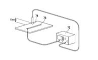
- electromagnetic wave noise transmitted from a shielded loop antenna 74 (loop diameter: 8 mm, distance from loop center to microstrip line 76: 10 mm) connected to a tracking generator incorporating a spectrum analyzer 72 with a coaxial cable.
- (1 MHz to 2 GHz) is received by a microstrip line 76 (Z: 50 ⁇ , substrate size: 50 mm ⁇ 80 mm, rear surface: entire ground) with a line length of 55 mm, and whether or not the microstrip line 76 is covered with an electromagnetic shielding member
- the reception characteristics were measured with a spectrum analyzer 72.
- a printed wiring board 1 having the structure shown in FIG. 1 (however, the electromagnetic wave shielding member 11 was used instead of the electromagnetic wave shielding member 10) was produced as follows.
- a sample having the same size (50 mm ⁇ 80 mm) as the microstrip substrate for evaluating the electromagnetic wave shielding function was cut out from the electromagnetic wave shielding member 11.
- the polyimide film side of the sample was pressed against the microstrip substrate shown in FIG. 6, and the microstrip line 76 was covered with the electromagnetic shielding member 11.
- a high frequency signal swept from 1 MHz to 2 GHz was output from the shield loop antenna 74, and reception characteristics were measured. Further, the reception characteristics in a state where the microstrip line 76 is not covered with the electromagnetic wave shielding member 12 were also measured.
- the reception characteristic is attenuated by several dB to a maximum of 20 dB when the microstrip line 76 is covered with the electromagnetic wave shielding member 11.
- a resist film was attached to the vapor deposition film 28 of the electromagnetic wave shielding member 11 (that is, the electromagnetic wave shielding layer 22), and exposure and development were performed to form a resist pattern having an anti-via portion and smaller than the outer dimensions of the printed wiring board.
- a single-sided flexible printed wiring board (printed wiring member 40) was bonded to both surfaces of the electromagnetic wave shielding member 11 using the insulating adhesive layer 30.
- a via hole 48 was formed by drilling around the anti-via portion.
- trimming of the outer shape was performed, and the printed wiring board 1 was obtained.
- the anti-via portion was filled with the insulating adhesive layer 30 without a gap.
- the electromagnetic shielding layer 22 was not exposed on the peripheral edge surface of the printed wiring board 1.
- a printed wiring board 2 having the structure shown in FIG. 2 was produced as follows. On one side of a polyimide film (base film 20, surface hardness (Vickers hardness): 560) of 280 mm ⁇ 280 mm ⁇ thickness 10 ⁇ m subjected to surface treatment for adhesion promotion, a gravure printing apparatus (manufactured by Kurashiki Boseki Co., Ltd., GP-10) is used to print soft ink (Japan Epoxy Resin Co., Ltd., # 1001 MEK solution with the same equivalent, Mitsubishi Gas Chemical Co., Gaskamine 240), and 1 mm ⁇ 3 mm soft material portion 26b (surface) The hardness (Vickers hardness): 260) was formed at a pitch of 5 mm.
- the reception characteristics of the electromagnetic wave shielding member 12 were measured in the same manner as in Example 1. Compared with the state in which the microstrip line 76 is not covered with the electromagnetic wave shielding member 12, the reception characteristic is attenuated by several dB to a maximum of 35 dB in the state in which the microstrip line 76 is covered with the electromagnetic wave shielding member 12.
- a resist film was attached to the vapor deposition film 28 of the electromagnetic wave shielding member 12 (that is, the electromagnetic wave shielding layer 22), and exposure and development were performed to form a resist pattern having an anti-via portion and smaller than the outer dimensions of the printed wiring board.
- a double-sided flexible wiring board (printed wiring member 43) was bonded to one side of the electromagnetic wave shielding member 12 using the insulating adhesive layer 30.
- the single-sided flexible wiring board (the printed wiring member 40 and the printed wiring member 41) was bonded to the outermost layer. Drilling was performed around the anti-via portion to form a via hole 48 and trimming of the outer shape to obtain the printed wiring board 2.
- the anti-via portion was filled with the insulating adhesive layer 30 without a gap.
- the electromagnetic shielding layer 22 was not exposed on the peripheral edge surface of the printed wiring board 2.
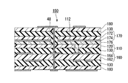
- a flexible printed wiring board 150 having the structure shown in FIG. 7 was produced. First, an insulating adhesive made of a nitrile rubber-modified epoxy resin is applied to the surface of a polyimide film 120 having a thickness of 10 ⁇ m so as to have a dry film thickness of 20 ⁇ m, and an insulating adhesive layer 130 is formed. Film 110 was obtained. A through-hole 112 for grounding was formed in the coverlay film 110.
- a flexible printed wiring board main body 160 in which a target conductor 164 was formed on the surface of a polyimide film 162 having a thickness of 12 ⁇ m was prepared.
- the coverlay film 110 was attached to the flexible printed wiring board main body 160 by hot pressing except for the end electrodes.
- Aluminum was physically vapor-deposited on the surface of the polyphenylene sulfide film 172 having a thickness of 3 ⁇ m by an ion beam evaporation method to form an aluminum vapor-deposited film 174 having a thickness of 100 nm, whereby an electromagnetic wave shielding film 170 was obtained.
- the electromagnetic wave shielding function was evaluated in the same manner as in Example 1 except that the grounded probe was brought into contact with the aluminum vapor deposition film 174 of the electromagnetic wave shielding film 170 and grounded.
- the electromagnetic wave shielding effect was equivalent to that in Example 2.
- a resist pattern was formed on the aluminum vapor deposition film 174 of the electromagnetic wave shielding film 170 in the same manner as in Example 2. This was etched using an etching solution of cupric chloride in an apparatus different from the etching solution used for etching the conductor of the flexible printed wiring board body.
- a conductive adhesive was prepared by dispersing 5% by volume of nickel particles having an average particle diameter of 10 ⁇ m in an insulating adhesive made of a nitrile rubber-modified epoxy resin.
- the conductive adhesive was applied to the surface of the aluminum vapor deposition film 174 so that the dry film thickness was 12 ⁇ m, and a conductive adhesive layer 176 was formed.
- a hole was made in the anti-via portion.
- the electromagnetic wave shielding film 170 was bonded to the cover lay film 110 side via the conductive adhesive layer 176.
- the aluminum vapor deposition film 174 of the electromagnetic wave shielding film 170 on the coverlay film 110 side was grounded to the ground circuit by the conductive adhesive layer 176 through the through hole 112.
- a single-sided flexible printed wiring board 180 is bonded to the outermost layer using an insulating adhesive layer 130, holes are drilled around the anti-via portion, via holes 48 are formed, external trimming is performed, and flexible printing is performed.
- a wiring board 150 was obtained.
- the printed wiring board of the present invention can be used as a flexible printed wiring board for electronic devices such as an optical module, a mobile phone, a digital camera, a game machine, a notebook computer, and a medical instrument, and thus is extremely useful industrially.
- Electromagnetic wave shield member 11 Electromagnetic wave shield member 12
- Electromagnetic wave shield member 20 Base film 22
- Deposition film 28a Deposition film 28b Deposition film 30 Insulating adhesive layer 40
- Printed wiring member 41 Printed wiring member 42
- Insulating layer 43 Printed wiring member 44 Target conductor 48 Via hole
Landscapes
- Engineering & Computer Science (AREA)
- Microelectronics & Electronic Packaging (AREA)
- Physics & Mathematics (AREA)
- Electromagnetism (AREA)
- Shielding Devices Or Components To Electric Or Magnetic Fields (AREA)
- Production Of Multi-Layered Print Wiring Board (AREA)
- Structure Of Printed Boards (AREA)
Abstract
Description
本願は、2010年4月15日に、日本に出願された特願2010-094028号に基づき優先権を主張し、その内容をここに援用する。
(1)耐熱プラスチックフィルム表面の銅箔配線回路上に、アンダーコート層、金属粉を含む導電ペーストを塗布したシールド層、およびオーバーコート層を順次設け、銅箔配線回路のグランドパターンと前記シールド層とが適宜の間隔で前記アンダーコート層を貫通して電気的に接続しているフレキシブルプリント配線板(特許文献1)。
(2)カバーレイフィルムの片面に金属薄膜層と金属フィラーを含む導電性接着剤層とを順次設けた電磁波シールドフィルムを、プリント回路のうちグランド回路の一部を除いて絶縁する絶縁層が設けられた基体フィルム上に、前記導電性接着剤層が前記絶縁層および前記グランド回路の一部と接着するように載置したフレキシブルプリント配線板(特許文献2)。
(i)金属粉を含むシールド層は、多くの異種材料界面を有しているため脆く、フレキシブル配線板の屈曲繰り返しに対し、十分な強度を有していない。
(ii)グランドパターンの一部を除く銅箔配線回路とシールド層との絶縁を保つためにアンダーコート層が必要であり、フレキシブルプリント配線板が厚くなる。
(iii)グランドパターンの一部とシールド層とを電気的に接続するために、アンダーコート層の一部に透孔を形成する必要があり、透孔の加工に手間がかかる。
(iv)シールド層がフレキシブルプリント配線板の周縁端面に露出しているため、水分の浸入や酸素との接触によって腐食して抵抗値が増大し、電磁波シールド機能が減退する。すなわち、電磁波シールド機能の信頼性が低い。
(v)シールド層が導電性ペーストを硬化させた硬化樹脂からなるため、エッチング液を用いてシールド層を所望の形状にエッチングできない。
(i)金属フィラーを含む導電性接着剤層は、多くの異種材料界面を有しているため脆く、フレキシブル配線板の屈曲繰り返しに対し、十分な強度を有していない。
(ii)グランド回路の一部を除くプリント回路と導電性接着剤層との絶縁を保つために絶縁層が必要であり、フレキシブルプリント配線板が厚くなる。
(iii)グランド回路の一部と導電性接着剤層とを電気的に接続するために、絶縁層の一部に貫通孔を形成する必要があり、貫通孔の加工に手間がかかる。
(iv)金属薄膜層がフレキシブルプリント配線板の周縁端面に露出しているため、水分の浸入や酸素との接触によって腐食して抵抗値が増大し、電磁波シールド機能が減退する。すなわち、電磁波シールド機能の信頼性が低い。
(v)金属薄膜層の材料(銀)とプリント回路の材料(銅)とが異なるため、同じエッチング液でエッチングできない。そのため、エッチング装置およびエッチング液を、金属薄膜層のエッチングおよびプリント回路のエッチングのために、それぞれ用意しなければならない。
本発明の第3の態様は、前記第1または第2の態様において、前記低抵抗部分の表面抵抗が、0.01~5Ωであり、前記高抵抗部分の表面抵抗が、前記低抵抗部分の表面抵抗の2~100倍であるプリント配線板である。
本発明の第4の態様は、前記第1~3のいずれか1つの態様において、前記高抵抗部分が、間隔を開けて繰り返し形成されているプリント配線板である。
(I)エッチング液を用いて、前記プリント配線部材の導電体を所望の形状にエッチングする工程。
(II)前記工程(I)と同じエッチング液を用いて、前記電磁波シールド部材の電磁波シールド層を所望の形状に、かつ下記工程(III)で得られたプリント配線板において電磁波シールド層がプリント配線板の周縁端面に露出しない大きさにエッチングする工程。 (III)前記プリント配線部材と前記電磁波シールド部材とを、前記対象導電体を覆うように前記電磁波シールド層が対向配置して絶縁性接着剤層を介して貼合した後、外形のトリミングを行う工程。
図1は、本発明のプリント配線板の一例を示す断面図である。
プリント配線板1は、基材フィルム20の一方の表面に、低抵抗部分22aと高抵抗部分22bとからなる電磁波シールド層22を有する電磁波シールド部材10と;電磁波シールド部材10の両面に、絶縁性接着剤層30を介して貼合された、絶縁層42の一方の表面に、電磁波シールドを施す対象となる対象導電体44を有するプリント配線部材40と;さらにこれらの表面に設けられた、絶縁層42の一方の表面に導電体46を有するプリント配線部材41とを備える。
また、ビアホール48の周辺部16にも、電磁波シールド層22は形成されておらず、よって、電磁波シールド層22は、ビアホール48から離間している。
プリント配線板2は、基材フィルム20の一方の表面に、低抵抗部分22aと高抵抗部分22bとからなる電磁波シールド層22を有する電磁波シールド部材12と;電磁波シールド部材12の一方の表面に、絶縁性接着剤層30を介して貼合された、絶縁層42の一方の表面に、電磁波シールドを施す対象となる対象導電体44を有するプリント配線部材40と;電磁波シールド部材12の他方の表面に、絶縁性接着剤層30を介して貼合された、絶縁層42の一方の表面に、電磁波シールドを施す対象となる対象導電体44を有し、絶縁層42の他方の表面に導電体46を有するプリント配線部材43と;さらにプリント配線部材43の表面に、絶縁性接着剤層30を介して貼合された、絶縁層42の一方の表面に導電体46を有するプリント配線部材41とを備える。
また、電磁波シールド部材12の周縁部14には、電磁波シールド層22は形成されておらず、よって、電磁波シールド層22は、プリント配線板2の周縁端面に露出していない。
また、ビアホール48の周辺部16にも、電磁波シールド層22は形成されておらず、よって、電磁波シールド層22は、ビアホール48から離間している。
電磁波シールド部材としては、例えば、下記の2種類の部材が挙げられる。
(α)基材フィルムが、前記基材フィルムの少なくとも一方の表面の一部に形成された凹凸部および前記凹凸部を除く非凹凸部を有し;電磁波シールド層が、前記凹凸部が形成された側の基材フィルムの表面に形成された導電性材料からなる蒸着膜である、電磁波シールドフィルム。
(β)基材フィルムが、前記基材フィルムの少なくとも一方の表面の一部に形成された、前記基材フィルムの表面よりも軟質な軟質材料部を有し;電磁波シールド層が、前記軟質材料部が形成された側の基材フィルムの表面に形成された導電性材料からなる蒸着膜である、電磁波シールドフィルム。
図3は、電磁波シールドフィルム(α)の一例を示す断面図である。
電磁波シールド部材10は、基材フィルム20の片面の一部に印刷を施して形成された印刷部(凹凸部24b)および前記印刷部を除く非印刷部(非凹凸部24a)を有する基材フィルム20と;印刷部が形成された側の基材フィルム20の表面に形成された導電性材料からなる蒸着膜28(すなわち電磁波シールド層22)と;蒸着膜28の表面を保護する保護層32とを有する。
なお、保護層32は、蒸着膜28側の表面に絶縁性接着剤層30を介してプリント配線部材を貼合する際には取り外される。
電磁波シールド部材11は、基材フィルム20の片面の一部を粗面化して形成された粗面化部(凹凸部24b)および前記粗面化部を除く非粗面化部(非凹凸部24a)を有する基材フィルム20と;前記粗面化部が形成された側の基材フィルム20の表面に形成された導電性材料からなる蒸着膜28(すなわち電磁波シールド層22)とを有する。
図5は、電磁波シールドフィルム(β)の一例を示す断面図である。
電磁波シールド部材12は、基材フィルム20の片面の一部に印刷を施して形成された、前記基材フィルム20の表面よりも軟質な軟質材料部26bおよび前記軟質材料部26bを除く基材フィルム20の表面26aを有する基材フィルム20と;軟質材料部26bが形成された側の基材フィルム20の表面に形成された導電性材料からなる蒸着膜28(電磁波シールド層22)と;蒸着膜28の表面を保護する保護層32とを有する。
なお、保護層32は、蒸着膜28側の表面に絶縁性接着剤層30を介してプリント配線部材を貼合する際には取り外される。
基材フィルム20は、凹凸部24bもしくは軟質材料部26b、および蒸着膜28を形成する際の下地となるフィルムである。
前記樹脂としては、ポリイミド、液晶ポリマー、ポリアラミド、ポリフェニレンサルファイド、ポリアミドイミド、ポリエーテルイミド、ポリエチレンナフタレート、ポリエチレンテレフタレート等が挙げられる。
基材フィルム20の表面抵抗は、1×10⁶Ω以上が好ましい。
基材フィルム20の厚さは、可とう性の点から、3~25μmが好ましい。基材フィルム20が薄いと、加工時の取り扱いが難しくなるため、微粘着のシート等の補強材を一時的に貼り付けても構わない。
凹凸部24bは、基材フィルム20の表面に印刷、粗面化処理、エッチング処理等を施して形成することができる。
粗面化処理としては、ブラスト処理等が挙げられる。基材フィルム20の材料がポリイミドの場合は、アルカリ処理等によっても粗面化できる。
エッチング処理としては、ウエットエッチング、ドライエッチング(レーザエッチング等)等が挙げられる。
算術平均粗さRaは、JIS B0651:1996の規定による算術平均粗さである。
凹凸部24bの1つあたりの最大長は、蒸着膜28がシールドする電磁波ノイズの波長λの1/4以下が好ましい。 凹凸部24bの1つあたりの面積は、蒸着膜28による電磁波シールド機能の点から、0.1~40mm2が好ましく、0.25~20mm2がより好ましい。
凹凸部24bの合計面積は、蒸着膜28の面積(100%)のうち、10~50%が好ましい。凹凸部24bの合計面積が10%未満では、高抵抗部分22bとなる蒸着膜28bによって、蒸着膜28を流れる高周波電流の十分な損失が図れない。凹凸部24bの合計面積が50%を超えると、電磁波シールド機能の維持のために、蒸着膜28を厚くする必要がある。
非凹凸部24a(非印刷部、非粗面化部、非エッチング部等)は、積極的に印刷、粗面化処理、エッチング処理等を行っていない面である。非凹凸部24aは、算術平均粗さRaが凹凸部24bよりも十分に小さければ、多少の凹凸を有していてもよい。
非凹凸部24aの算術平均粗さRaは、0.1μm以下が好ましい。非凹凸部24aの算術平均粗さRaが0.1μm以下であれば、非凹凸部24aに形成される蒸着膜28が厚くなり、前記低抵抗部分22aとなる蒸着膜28aの表面抵抗が十分に低くなる。
軟質材料部26bは、軟質材料からなる。
軟質材料とは、基材フィルム20の表面26aを構成している材料よりも軟質な材料であり、具体的には、硬度(ビッカース硬さ)が基材フィルム20の表面26aよりも低い材料である。
印刷法としては、グラビア印刷法、スクリーン印刷法等が挙げられる。
軟質インキとしては、ウレタン樹脂、ポリエステル樹脂、ポリアミド樹脂、エポキシ樹脂、合成ゴム等をバインダーとした軟質インキ等が挙げられる。
軟質材料部26bの1つあたりの最大長は、蒸着膜28がシールドする電磁波ノイズの波長λの1/4以下が好ましい。 軟質材料部26bの1つあたりの面積は、蒸着膜28による電磁波シールド機能の点から、0.1~40mm2が好ましく、0.25~20mm2がより好ましい。
軟質材料部26bの合計面積は、蒸着膜28の面積(100%)のうち、10~50%が好ましい。軟質材料部26bの合計面積が10%未満では、高抵抗部分22bとなる蒸着膜28bによって、蒸着膜28を流れる高周波電流の十分な損失が図れない。軟質材料部26bの合計面積が50%を超えると、電磁波シールド機能の維持のために、蒸着膜28を厚くする必要がある。
蒸着膜28は、基材フィルム20の表面、および凹凸部24bもしくは軟質材料部26bの表面に、導電性材料を物理的に蒸着させて形成される導電性材料からなる膜であり、電磁波シールド部材における電磁波シールド層22となる。
前記導電性材料としては、金属または導電性セラミックスが挙げられる。前記金属としては、金、銀、銅、アルミニウム、またはニッケルが好ましく、銅が特に好ましい。
蒸着膜28b(高抵抗部分22b)の表面抵抗は、蒸着膜28を流れる高周波電流を十分に損失させる点から、蒸着膜28aの表面抵抗の2~100倍が好ましい。
蒸着膜28の厚さは、耐屈曲特性の点から、50~200nmが好ましい。
保護層32は、外部の接触から蒸着膜28を保護する層であり、電磁波シールド部材をプリント配線板の最外層に用いる場合は必要となる。
保護層32は、樹脂またはゴム弾性体からなる層である。保護層32の表面抵抗は、1×10⁶Ω以上が好ましい。
前記フィルムの材料としては、基材フィルム20の材料と同様の材料が挙げられる。
保護層32の厚さは、可とう性の点から、3~25μmが好ましい。
絶縁性接着剤層30は、電磁波シールド部材とプリント配線部材とを貼合させる層である。
プリント配線部材は、絶縁層の表面に導電体を有するものである。
導電体は、導電性材料からなり、プリント配線板における信号線路、電源線路、電源層、グランド線路、グランド層等を構成する材料である。
前記銅箔の厚さは、3~50μmが好ましい。
絶縁層としては、絶縁性フィルムからなる層、硬化性樹脂組成物を硬化させてなる層等が挙げられる。
前記絶縁性フィルムは、耐熱性を有するフィルムが好ましく、ポリイミドフィルム、液晶ポリマーフィルム等がより好ましい。
前記絶縁性フィルムの厚さは、5~50μmが好ましく、屈曲性の点から、6~25μmがより好ましく、10~25μmが特に好ましい。
前記エポキシ樹脂を含む硬化性樹脂組成物は、必要に応じて、さらに、アルコキシシラン、硬化剤、硬化促進剤、可とう性付与剤等を含んでいてもよい。
前記硬化性樹脂組成物を硬化させてなる層の厚さは、0.1~10μmが好ましい。
以上説明したプリント配線板にあっては、後述する理由から電磁波シールド部材の電磁波シールド層(蒸着膜)をプリント部材のグランド(グランド線路、グランド層等)に接続させなくても、電磁波シールド機能を有する。そのため、電磁波シールド層をグランドに接続させるために接着剤層に導電性を付与する必要がなくなり、フレキシブルプリント配線板においては屈曲性が向上する。また、接着剤層が導電性を有さないため、接着剤層とプリント配線部材の導電体との間を絶縁するための絶縁層が不要となり、フレキシブルプリント配線板においては薄肉化が可能となる。
また、電磁波シールド層がプリント配線板のビアホールまたはスルーホールから離間しているため、電磁波シールド層とビアホールまたはスルーホールにおける導電体とが短絡することがない。
また、電磁波シールド層および導電体が、同種の導電材料からなるため、製造の際には電磁波シールド層および導電体を同じエッチング液でエッチングできる。
電磁波シールド層(蒸着膜)をグランドに接続させなくてもよい理由としては、下記のことが考えられる。
基材フィルム20の表面に形成された比較的表面抵抗の低い蒸着膜28a(すなわち低抵抗部分22a)は、グランドに接続していないことからアンテナとして働く。そのため、反射しきれなかった電磁波ノイズは蒸着膜28a内を高周波電流となって流れ、その縁端部から再度放出される。再放出時には、蒸着膜28aの縁端部に電磁界の変動が生まれ、そのうち磁界変動に伴う渦電流が、比較的表面抵抗の高い蒸着膜28b(すなわち高抵抗部分22b)に流れて、熱損失するため、電磁波ノイズのエネルギーが減衰すると考えられる。
本発明のプリント配線板の製造方法は、下記の工程(I)~(III)を有する方法である。
(I)エッチング液を用いて、プリント配線部材の導電体を所望の形状にエッチングする工程。
(II)工程(I)と同じエッチング液を用いて、電磁波シールド部材の電磁波シールド層を所望の形状に、かつ工程(III)で得られたプリント配線板において電磁波シールド層がプリント配線板の周縁端面に露出しない大きさにエッチングする工程。 (III)プリント配線部材と電磁波シールド部材とを、対象導電体を覆うように電磁波シールド層が対向配置して絶縁性接着剤層を介して貼合した後、外形のトリミングを行う工程。
プリント配線部材の絶縁層の表面の全体に設けられた膜状の導電体を、公知の方法によってエッチングして、信号線路、電源線路、電源層、グランド線路、グランド層等の形状に加工する。
エッチング液としては、一般的なエッチング液を用いればよく、例えば、塩化第二銅または塩化第二鉄を主成分とする水溶液が挙げられる。
電磁波シールド部材の基材フィルムの表面の全体に設けられた膜状の電磁波シールド層(蒸着膜)の導電体を、公知の方法によってエッチングして、対象導体を電磁波シールドするのに必要な形状に加工する。
前記アンチビア部は、電磁波シールド部材に穴あけしても形成できるが、微細な除去加工ができず、基材フィルムの強度を弱め、破断するおそれもあるため、基材フィルムを残存させ、電磁波シールド層だけ除去するエッチングによって形成することが好ましい。
プリント配線部材と電磁波シールド部材とを、対象導電体を覆うように電磁波シールド層が対向配置して絶縁性接着剤層を介して貼合し、プリント配線板前駆体を得る。
前記絶縁性接着剤層を設ける方法としては、シート状の絶縁性接着剤を貼着する方法、液状の絶縁性接着剤を塗布する方法等が挙げられる。
前記プリント配線板前駆体の周縁の余分な部分を切断して外形のトリミングを行い、プリント配線板を得る。
透過型電子顕微鏡(日立製作所社製、H9000NAR)を用いて断面を観察し、各層の5箇所の厚さを測定し、平均した。
石英ガラス上に金を蒸着して形成した、2本の薄膜金属電極(長さ:10mm、幅:5mm、電極間距離:10mm)を用い、前記電極上に被測定物を置いた。次いで、前記被測定物上から、前記被測定物の10mm×20mmの領域を50gの荷重で押し付け、1mA以下の測定電流で電極間の抵抗を測定し、この値を表面抵抗とした。
ダイナミック超微小硬度計(島津製作所社製、DUH-211)を用い、ビッカース硬さを測定した。押し込み量は、最低0.1μmとし、サブミクロンオーダーの厚さの試料も測定可能とした。
電磁波シールド部材の電磁波シールド機能を評価した。図6に示すシステムを用い、スペクトラムアナライザ72を内蔵したトラッキングジェネレータに同軸ケーブルで接続したシールドループアンテナ74(ループ径:8mm、ループ中心からマイクロストリップライン76までの距離:10mm)から発信した電磁波ノイズ(1MHzから2GHz)をライン長55mmのマイクロストリップライン76(Z:50Ω、基板サイズ:50mm×80mm、背面:全面グランド)で受け、電磁波シールド部材でマイクロストリップライン76を覆うか否かの状態で受信特性をスペクトラムアナライザ72で測定した。
図1に示す構造を有するプリント配線板1(ただし、電磁波シールド部材10の代わりに電磁波シールド部材11を用いた。)を以下のように作製した。
280mm×280mm×厚さ12.5μmのポリイミドフィルム(基材フィルム20、算術平均粗さRa:0.08μm)の片面に、1mm×3mmの孔が5mmのピッチで形成されたマスクを被せ、ブラスト処理を行い、孔に対応した位置に粗面化部(凹凸部24b、算術平均粗さRa:1.6μm)を形成した。
前記粗面化部が形成された側のポリイミドフィルムの表面に、マグネトロンスパッタ法にて銅を物理的に蒸着させ銅蒸着膜(蒸着膜28)を形成し、電磁波シールド部材11を得た。非凹凸部24aに形成された蒸着膜28aの表面抵抗は0.5Ωであり、凹凸部24bに形成された蒸着膜28bの表面抵抗は1.8Ωであった。
図6に示すマイクロストリップ基板に前記サンプルのポリイミドフィルム側を押し当て、マイクロストリップライン76を電磁波シールド部材11で覆った。シールドループアンテナ74から1MHzから2GHzの掃引された高周波信号を出力し、受信特性を測定した。また、マイクロストリップライン76が電磁波シールド部材12で覆われていない状態での受信特性も測定した。マイクロストリップライン76が電磁波シールド部材11で覆われていない状態に比べ、マイクロストリップライン76が電磁波シールド部材11で覆われた状態では、受信特性は数dBから最大20dBほど減衰した。
図2に示す構造を有するプリント配線板2を以下のように作製した。
接着促進用に表面処理を施した、280mm×280mm×厚さ10μmのポリイミドフィルム(基材フィルム20、表面の硬度(ビッカース硬さ):560)の片面に、グラビア印刷装置(倉敷紡績社製、GP-10)を用い、軟質インキ(ジャパンエポキシレジン社製、#1001のMEK溶液に同当量の三菱ガス化学社製、Gaskamine240を配合)を印刷して、1mm×3mmの軟質材料部26b(表面の硬度(ビッカース硬さ):260)を5mmのピッチで複数形成した。
軟質材料部26bが形成された側のポリイミドフィルムの表面26aおよび軟質材料部26bの表面に、EB蒸着法にて銅を物理的に蒸着させ蒸着膜28を形成し、電磁波シールド部材12を得た。ポリイミドフィルムの表面26aに形成された蒸着膜28aの表面抵抗は0.24Ωであり、軟質材料部26bの表面に形成された蒸着膜28bの表面抵抗は0.32Ωであった。
図7に示す構造を有するフレキシブルプリント配線板150を作製した。
まず、厚さ10μmのポリイミドフィルム120の表面に、ニトリルゴム変性エポキシ樹脂からなる絶縁性接着剤を、乾燥膜厚が20μmになるように塗布し、絶縁性接着剤層130を形成し、カバーレイフィルム110を得た。カバーレイフィルム110には接地のための透孔112を形成した。
フレキシブルプリント配線板本体160に、端部電極を除いてカバーレイフィルム110を熱プレスにより貼着した。
電磁波シールドフィルム170のアルミニウム蒸着膜174に、接地されているプローブを接触させて接地した以外は、実施例1と同様にして電磁波シールド機能の評価を行った。電磁波シールド効果は実施例2と同等であった。
電磁波シールドフィルム170のアルミニウム蒸着膜174に、実施例2と同様にレジストパターンを形成した。これを、フレキシブルプリント配線板本体の導電体のエッチングに用いるエッチング液と異なる装置の塩化第二銅のエッチング液を用いて、エッチングした。
アルミニウム蒸着膜174の表面に、前記導電性接着剤を、乾燥膜厚が12μmになるように塗布し、導電性接着剤層176を形成した。ついで、アンチビア部に穴あけを行った。
さらに最表層に、片面フレキシブルプリント配線板180を、絶縁性接着剤層130を用いて貼合し、前記アンチビア部を中心に穴あけを行い、ビアホール48を形成し、外形のトリミングを行い、フレキシブルプリント配線板150を得た。
前記アンチビア部には絶縁性接着剤層130が充分に充填されず、空隙があった。フレキシブルプリント配線板150の周縁端面にはアルミニウム蒸着膜174の露出はなかったが、蒸着膜としてアルミニウムを用いたため、エッチング装置およびエッチング液を別に用意しなければならず合理的でなかった。
2 プリント配線板
10 電磁波シールド部材
11 電磁波シールド部材
12 電磁波シールド部材
20 基材フィルム
22 電磁波シールド層
22a 低抵抗部分
22b 高抵抗部分
24a 非凹凸部
24b 凹凸部
26a 表面
26b 軟質材料部
28 蒸着膜
28a 蒸着膜
28b 蒸着膜
30 絶縁性接着剤層
40 プリント配線部材
41 プリント配線部材
42 絶縁層
43 プリント配線部材
44 対象導電体
48 ビアホール
Claims (7)
- 絶縁層の少なくとも一方の表面に、電磁波シールドを施す対象となる対象導電体を有するプリント配線部材と、
基材フィルムの少なくとも一方の表面に、低抵抗部分と高抵抗部分とからなる電磁波シールド層を有する電磁波シールド部材と、
を備え、
前記プリント配線部材と前記電磁波シールド部材とが、前記対象導電体を覆うように前記電磁波シールド層が離間して対向配置して、絶縁性接着剤層を介して貼合されたプリント配線板であって、
前記電磁波シールド層および前記対象導電体が、同種の導電材料からなり、
前記電磁波シールド層が、前記プリント配線板の周縁端面に露出していない、プリント配線板。 - 前記電磁波シールド層が、前記プリント配線板のビアホールまたはスルーホールから離間している、請求項1に記載のプリント配線板。
- 前記低抵抗部分の表面抵抗が、0.01~5Ωであり、
前記高抵抗部分の表面抵抗が、前記低抵抗部分の表面抵抗の2~100倍である、請求項1に記載のプリント配線板。 - 前記高抵抗部分が、間隔を開けて繰り返し形成されている、請求項1に記載のプリント配線板。
- 前記基材フィルムが、前記基材フィルムの少なくとも一方の表面の一部に形成された、前記基材フィルムの表面よりも軟質な軟質材料部を有し、
前記電磁波シールド層が、前記軟質材料部が形成された側の前記基材フィルムの表面に形成された導電性材料からなる蒸着膜であり、
前記基材フィルムの表面に形成された蒸着膜が、低抵抗部分となり、
前記軟質材料部の表面に形成された蒸着膜が、高抵抗部分となる、請求項1に記載のプリント配線板。 - 前記基材フィルムが、前記基材フィルムの少なくとも一方の表面の一部に形成された凹凸部および前記凹凸部を除く非凹凸部を有し、
前記電磁波シールド層が、前記凹凸部が形成された側の前記基材フィルムの表面に形成された導電性材料からなる蒸着膜であり、
前記非凹凸部に形成された蒸着膜が、低抵抗部分となり、
前記凹凸部に形成された蒸着膜が、高抵抗部分となる、請求項1に記載のプリント配線板。 - 請求項1~6のいずれか一項に記載のプリント配線板を製造する方法であって、
下記の工程(I)~(III)を有する、プリント配線板の製造方法。
(I)エッチング液を用いて、前記プリント配線部材の導電体を所望の形状にエッチングする工程。
(II)前記工程(I)と同じエッチング液を用いて、前記電磁波シールド部材の電磁波シールド層を所望の形状に、かつ下記工程(III)で得られたプリント配線板において電磁波シールド層がプリント配線板の周縁端面に露出しない大きさにエッチングする工程。 (III)前記プリント配線部材と前記電磁波シールド部材とを、前記対象導電体を覆うように前記電磁波シールド層が対向配置して絶縁性接着剤層を介して貼合した後、外形のトリミングを行う工程。
Priority Applications (2)
| Application Number | Priority Date | Filing Date | Title |
|---|---|---|---|
| US13/639,640 US9006581B2 (en) | 2010-04-15 | 2011-04-11 | Printed wiring board and method of manufacture thereof |
| CN201180019224.1A CN102960078B (zh) | 2010-04-15 | 2011-04-11 | 印刷配线板及其制造方法 |
Applications Claiming Priority (2)
| Application Number | Priority Date | Filing Date | Title |
|---|---|---|---|
| JP2010-094028 | 2010-04-15 | ||
| JP2010094028A JP5380355B2 (ja) | 2010-04-15 | 2010-04-15 | プリント配線板およびその製造方法 |
Publications (1)
| Publication Number | Publication Date |
|---|---|
| WO2011129299A1 true WO2011129299A1 (ja) | 2011-10-20 |
Family
ID=44798672
Family Applications (1)
| Application Number | Title | Priority Date | Filing Date |
|---|---|---|---|
| PCT/JP2011/059001 Ceased WO2011129299A1 (ja) | 2010-04-15 | 2011-04-11 | プリント配線板およびその製造方法 |
Country Status (4)
| Country | Link |
|---|---|
| US (1) | US9006581B2 (ja) |
| JP (1) | JP5380355B2 (ja) |
| CN (1) | CN102960078B (ja) |
| WO (1) | WO2011129299A1 (ja) |
Cited By (2)
| Publication number | Priority date | Publication date | Assignee | Title |
|---|---|---|---|---|
| JP2014049498A (ja) * | 2012-08-29 | 2014-03-17 | Shin Etsu Polymer Co Ltd | 電磁波シールドフィルム、電磁波シールドフィルムの製造方法、フレキシブルプリント配線板およびフレキシブルプリント配線板の製造方法 |
| CN110769669A (zh) * | 2018-07-27 | 2020-02-07 | 广州方邦电子股份有限公司 | 电磁屏蔽膜、线路板及电磁屏蔽膜的制备方法 |
Families Citing this family (14)
| Publication number | Priority date | Publication date | Assignee | Title |
|---|---|---|---|---|
| US10537028B2 (en) * | 2014-06-30 | 2020-01-14 | 3M Innovative Properties Company | Metallic microstructures with reduced-visibility and methods for producing same |
| WO2016049109A2 (en) | 2014-09-25 | 2016-03-31 | Drexel University | Physical forms of mxene materials exhibiting novel electrical and optical characteristics |
| EP3265211B1 (en) | 2015-03-04 | 2019-12-04 | Drexel University | Nanolaminated 2-2-1 max-phase compositions |
| WO2017011044A2 (en) | 2015-04-20 | 2017-01-19 | Drexel University | Two-dimensional, ordered, double transition metals carbides having a nominal unit cell composition m'2m"nxn+1 |
| EP3232751B1 (de) * | 2016-04-12 | 2018-07-18 | MD Elektronik GmbH | Elektrische steckkupplungsvorrichtung |
| KR102200472B1 (ko) * | 2016-04-22 | 2021-01-08 | 한국과학기술연구원 | Emi 차폐용 2차원 금속 탄화물, 질화물 및 탄질화물 필름 및 복합체 |
| US10088642B2 (en) | 2016-11-09 | 2018-10-02 | International Business Machines Corporation | Coaxial wire and optical fiber trace via hybrid structures and methods to manufacture |
| CN109892020B (zh) * | 2017-02-13 | 2022-03-04 | 拓自达电线株式会社 | 接地构件、屏蔽印制线路板及屏蔽印制线路板的制造方法 |
| US11278862B2 (en) | 2017-08-01 | 2022-03-22 | Drexel University | Mxene sorbent for removal of small molecules from dialysate |
| US10398025B2 (en) * | 2017-11-09 | 2019-08-27 | International Business Machines Corporation | Peripheral end face attachment of exposed copper layers of a first printed circuit board to the surface of a second printed circuit board by surface mount assembly |
| US10321564B2 (en) | 2017-11-09 | 2019-06-11 | International Business Machines Corporation | Solder assembly of pins to the peripheral end face of a printed circuit board |
| KR102869375B1 (ko) * | 2020-07-28 | 2025-10-14 | 삼성전자주식회사 | Fpcb 조립체 및 이를 포함하는 전자 기기 |
| EP4016552B1 (en) * | 2020-12-15 | 2026-03-18 | Nexans | Lead-free water barrier |
| CN114641126B (zh) * | 2021-02-09 | 2024-03-08 | 广州方邦电子股份有限公司 | 电磁屏蔽膜及线路板 |
Citations (3)
| Publication number | Priority date | Publication date | Assignee | Title |
|---|---|---|---|---|
| JPH02249291A (ja) * | 1989-03-23 | 1990-10-05 | Hitachi Cable Ltd | プリント配線基板 |
| JP2006156946A (ja) * | 2004-11-04 | 2006-06-15 | Kitagawa Ind Co Ltd | 電磁波シールドフィルム |
| JP2009283901A (ja) * | 2008-04-21 | 2009-12-03 | Shin Etsu Polymer Co Ltd | カバーレイフィルムおよびフレキシブルプリント配線板 |
Family Cites Families (12)
| Publication number | Priority date | Publication date | Assignee | Title |
|---|---|---|---|---|
| US4647714A (en) * | 1984-12-28 | 1987-03-03 | Sohwa Laminate Printing Co., Ltd. | Composite sheet material for magnetic and electronic shielding and product obtained therefrom |
| JPH0828575B2 (ja) * | 1988-06-03 | 1996-03-21 | 株式会社ジャパンエナジー | プリント配線板の製造方法 |
| JPH0634473B2 (ja) | 1988-07-23 | 1994-05-02 | 堺電子工業株式会社 | 電磁波遮蔽付フレキシブルプリント回路形成体 |
| JPH02139993A (ja) * | 1988-11-21 | 1990-05-29 | Toshiba Corp | 印刷配線基板の製造方法 |
| JP2631544B2 (ja) | 1989-01-27 | 1997-07-16 | 日本シイエムケイ株式会社 | プリント配線板 |
| JP2663011B2 (ja) * | 1989-03-15 | 1997-10-15 | 日本シイエムケイ株式会社 | シールド層を備えるプリント配線板 |
| JP2631548B2 (ja) * | 1989-03-15 | 1997-07-16 | 日本シイエムケイ株式会社 | シールド層を備えるプリント配線板 |
| JP2777747B2 (ja) * | 1990-11-26 | 1998-07-23 | 東亞合成株式会社 | 電磁波シールド層を有するプリント抵抗器内蔵多層プリント回路板 |
| JPH069166U (ja) * | 1992-07-03 | 1994-02-04 | 日本シイエムケイ株式会社 | 電磁波シールドを有するプリント配線板 |
| JP2000269632A (ja) * | 1999-03-17 | 2000-09-29 | Tatsuta Electric Wire & Cable Co Ltd | シールドフレキシブルプリント配線板の製造方法、シールドフレキシブルプリント配線板用補強シールドフィルム及びシールドフレキシブルプリント配線板 |
| US8134084B2 (en) * | 2006-06-30 | 2012-03-13 | Shin-Etsu Polymer Co., Ltd. | Noise-suppressing wiring-member and printed wiring board |
| CN101489346B (zh) * | 2008-01-15 | 2011-11-16 | 欣兴电子股份有限公司 | 线路板的图案化结构 |
-
2010
- 2010-04-15 JP JP2010094028A patent/JP5380355B2/ja not_active Expired - Fee Related
-
2011
- 2011-04-11 WO PCT/JP2011/059001 patent/WO2011129299A1/ja not_active Ceased
- 2011-04-11 CN CN201180019224.1A patent/CN102960078B/zh not_active Expired - Fee Related
- 2011-04-11 US US13/639,640 patent/US9006581B2/en not_active Expired - Fee Related
Patent Citations (3)
| Publication number | Priority date | Publication date | Assignee | Title |
|---|---|---|---|---|
| JPH02249291A (ja) * | 1989-03-23 | 1990-10-05 | Hitachi Cable Ltd | プリント配線基板 |
| JP2006156946A (ja) * | 2004-11-04 | 2006-06-15 | Kitagawa Ind Co Ltd | 電磁波シールドフィルム |
| JP2009283901A (ja) * | 2008-04-21 | 2009-12-03 | Shin Etsu Polymer Co Ltd | カバーレイフィルムおよびフレキシブルプリント配線板 |
Cited By (3)
| Publication number | Priority date | Publication date | Assignee | Title |
|---|---|---|---|---|
| JP2014049498A (ja) * | 2012-08-29 | 2014-03-17 | Shin Etsu Polymer Co Ltd | 電磁波シールドフィルム、電磁波シールドフィルムの製造方法、フレキシブルプリント配線板およびフレキシブルプリント配線板の製造方法 |
| CN110769669A (zh) * | 2018-07-27 | 2020-02-07 | 广州方邦电子股份有限公司 | 电磁屏蔽膜、线路板及电磁屏蔽膜的制备方法 |
| CN110769669B (zh) * | 2018-07-27 | 2024-02-06 | 广州方邦电子股份有限公司 | 电磁屏蔽膜、线路板及电磁屏蔽膜的制备方法 |
Also Published As
| Publication number | Publication date |
|---|---|
| JP2011228342A (ja) | 2011-11-10 |
| CN102960078A (zh) | 2013-03-06 |
| CN102960078B (zh) | 2015-09-02 |
| US20130092428A1 (en) | 2013-04-18 |
| JP5380355B2 (ja) | 2014-01-08 |
| US9006581B2 (en) | 2015-04-14 |
Similar Documents
| Publication | Publication Date | Title |
|---|---|---|
| JP5380355B2 (ja) | プリント配線板およびその製造方法 | |
| JP5150534B2 (ja) | カバーレイフィルム、その製造方法およびフレキシブルプリント配線板 | |
| EP2222144B1 (en) | Noise suppressing structure and printed wiring board | |
| JP5866266B2 (ja) | 電磁波シールドフィルム、電磁波シールドフィルムの製造方法、およびフレキシブルプリント配線板の製造方法 | |
| JP5202377B2 (ja) | カバーレイフィルムおよびフレキシブルプリント配線板 | |
| JP2014090162A (ja) | カバーレイフィルムおよびフレキシブルプリント配線板 | |
| US8541686B2 (en) | Wiring member and method for producing the same | |
| CN102124821B (zh) | 印刷配线板 | |
| JP5193903B2 (ja) | カバーレイフィルム、フレキシブルプリント配線板および光トランシーバ | |
| CN102316665A (zh) | 柔性电路板及其制作方法 | |
| CN206506769U (zh) | 接地膜及具有接地膜的印制电路板 | |
| JP4916803B2 (ja) | 多層プリント回路基板 | |
| JP5439104B2 (ja) | カバーレイフィルム、その製造方法およびフレキシブルプリント配線板 | |
| JP2010153534A (ja) | カバーレイフィルム、その製造方法およびフレキシブルプリント配線板 | |
| JP2005277262A (ja) | 電磁波シールドフィルム | |
| JP5292033B2 (ja) | プリント配線板 | |
| US20070087556A1 (en) | Method and mesh reference structures for implementing Z-axis cross-talk reduction through copper sputtering onto mesh reference planes |
Legal Events
| Date | Code | Title | Description |
|---|---|---|---|
| WWE | Wipo information: entry into national phase |
Ref document number: 201180019224.1 Country of ref document: CN |
|
| 121 | Ep: the epo has been informed by wipo that ep was designated in this application |
Ref document number: 11768820 Country of ref document: EP Kind code of ref document: A1 |
|
| NENP | Non-entry into the national phase |
Ref country code: DE |
|
| WWE | Wipo information: entry into national phase |
Ref document number: 13639640 Country of ref document: US |
|
| 122 | Ep: pct application non-entry in european phase |
Ref document number: 11768820 Country of ref document: EP Kind code of ref document: A1 |