WO2011125389A1 - 透明圧電シートをそれぞれ有するフレーム付透明圧電シート、タッチパネル、および電子装置 - Google Patents
透明圧電シートをそれぞれ有するフレーム付透明圧電シート、タッチパネル、および電子装置 Download PDFInfo
- Publication number
- WO2011125389A1 WO2011125389A1 PCT/JP2011/054521 JP2011054521W WO2011125389A1 WO 2011125389 A1 WO2011125389 A1 WO 2011125389A1 JP 2011054521 W JP2011054521 W JP 2011054521W WO 2011125389 A1 WO2011125389 A1 WO 2011125389A1
- Authority
- WO
- WIPO (PCT)
- Prior art keywords
- transparent
- plate electrode
- flat plate
- transparent flat
- piezoelectric sheet
- Prior art date
- Legal status (The legal status is an assumption and is not a legal conclusion. Google has not performed a legal analysis and makes no representation as to the accuracy of the status listed.)
- Ceased
Links
Images



Classifications
-
- G—PHYSICS
- G01—MEASURING; TESTING
- G01L—MEASURING FORCE, STRESS, TORQUE, WORK, MECHANICAL POWER, MECHANICAL EFFICIENCY, OR FLUID PRESSURE
- G01L1/00—Measuring force or stress, in general
- G01L1/16—Measuring force or stress, in general using properties of piezoelectric devices
-
- G—PHYSICS
- G06—COMPUTING OR CALCULATING; COUNTING
- G06F—ELECTRIC DIGITAL DATA PROCESSING
- G06F3/00—Input arrangements for transferring data to be processed into a form capable of being handled by the computer; Output arrangements for transferring data from processing unit to output unit, e.g. interface arrangements
- G06F3/01—Input arrangements or combined input and output arrangements for interaction between user and computer
- G06F3/03—Arrangements for converting the position or the displacement of a member into a coded form
- G06F3/041—Digitisers, e.g. for touch screens or touch pads, characterised by the transducing means
-
- G—PHYSICS
- G06—COMPUTING OR CALCULATING; COUNTING
- G06F—ELECTRIC DIGITAL DATA PROCESSING
- G06F2203/00—Indexing scheme relating to G06F3/00 - G06F3/048
- G06F2203/041—Indexing scheme relating to G06F3/041 - G06F3/045
- G06F2203/04105—Pressure sensors for measuring the pressure or force exerted on the touch surface without providing the touch position
-
- G—PHYSICS
- G06—COMPUTING OR CALCULATING; COUNTING
- G06F—ELECTRIC DIGITAL DATA PROCESSING
- G06F3/00—Input arrangements for transferring data to be processed into a form capable of being handled by the computer; Output arrangements for transferring data from processing unit to output unit, e.g. interface arrangements
- G06F3/01—Input arrangements or combined input and output arrangements for interaction between user and computer
- G06F3/03—Arrangements for converting the position or the displacement of a member into a coded form
- G06F3/041—Digitisers, e.g. for touch screens or touch pads, characterised by the transducing means
- G06F3/0414—Digitisers, e.g. for touch screens or touch pads, characterised by the transducing means using force sensing means to determine a position
Definitions
- the present invention relates to a transparent piezoelectric sheet with a frame each having a transparent piezoelectric sheet, a touch panel, and an electronic device.
- a display and input device in which a touch panel, which is an input device, is installed on the front surface of a display device such as a liquid crystal display has been put into practical use and is used for an operation panel of a portable device such as a mobile phone and a home appliance.
- a display and input device using a touch panel enables a user to operate the device intuitively by pressing a display on the screen.
- the touch panel that has been put to practical use so far can only detect the position pressed by the user (sometimes referred to as a touch position in the present specification), and the strength pressed by the user (that is, the height of the press). (Strength), which may be referred to as touch pressure in this specification) could not be detected.
- the touch panel is installed on the front surface of the display device. Therefore, in order to improve the visibility of display on the display device, the touch panel needs to have high transparency.
- Patent Document 1 discloses a piezoelectric body used as a member of electronic paper and one of the piezoelectric bodies.
- a touch panel unit having a first electrode provided on the side and a second electrode provided on the other side of the piezoelectric body is disclosed.
- Patent Document 2 discloses a first sensor system that is coupled to a touch screen and determines a set of position coordinates for each contact of the touch screen, and is coupled to the touch screen and is touched by a first type object.
- a touch screen system comprising: a second sensor system that confirms each touch on the screen and invalidates each touch on the touch screen with a second type of object; Specifically, as the first sensor system, a force sensor disposed outside the visual region of the LCD is disclosed.
- Patent Document 3 a transparent pressure-sensitive layer having piezoelectricity and a pair of transparent conductive film layers opposed to each other via the transparent pressure-sensitive layer are formed between a pair of opposed transparent substrates.
- a transparent piezoelectric sensor is disclosed.
- the transparent piezoelectric sheet for touch pressure detection has a piezoelectric property on the entire main surface of the transparent piezoelectric film used for the touch pressure detection from the viewpoint of widening the effective area of touch pressure detection.
- Such a transparent piezoelectric sheet for touch pressure detection is preferably used in combination with a touch panel for touch position detection.
- the transparent piezoelectric sheet for touch pressure detection preferably has a size in plan view that does not exceed the size of the touch position detection touch panel. It is desired that the touch pressure can be detected in the region. It is generally known that the ratio of the area of the detection effective area to the area of the touch position detection touch panel is high, but it is generally known that the entire detection effective area of the touch position detection touch panel is known. In order to be able to detect a touch pressure in a region, a stricter requirement is inevitably imposed on a transparent piezoelectric sheet for touch pressure detection than a touch panel for touch position detection.
- the entire surfaces of the two main surfaces of the transparent piezoelectric sheet for touch pressure detection may be covered with transparent flat electrodes, respectively.
- the transparent piezoelectric sheet for detecting the touch pressure is preferably covered with a frame at the periphery thereof from the viewpoint of ease of handling. In this case, if the touch pressure can be detected on the entire surface of the transparent piezoelectric sheet for detecting the touch pressure, the transparent piezoelectric sheet does not detect the pressure applied by the frame, and the target touch pressure cannot be detected. Or significantly reduce its accuracy.
- the transparent piezoelectric sheet for detecting the touch pressure may be used without being housed in the frame, as it is, as a member of the electronic device, arranged in a housing having an opening.
- the transparent piezoelectric sheet detects the pressure applied by the inner edge, as in the case of the frame. As a result, it becomes impossible to detect the original touch pressure, or the accuracy thereof is significantly reduced.
- An object of the present invention is to provide a transparent piezoelectric sheet with a frame that can detect a touch pressure with a larger area and higher accuracy, has a low manufacturing cost, and is excellent in appearance.
- the above-mentioned problem is dared to change the size of the transparent flat plate electrode portions of the two transparent electrodes on both sides of the transparent piezoelectric film, and further to the larger transparent flat plate electrode portion (hereinafter referred to as the first transparent flat plate electrode portion). ) Completely overlaps with the inner edge of the frame or housing described above in plan view, and the smaller transparent flat plate electrode portion (hereinafter referred to as the second transparent flat plate electrode portion) is completely the frame or the It can be solved by arranging it so as not to overlap with the inner edge.
- the transparent piezoelectric sheet with a frame includes one transparent piezoelectric film containing an organic polymer, and one first piezoelectric element disposed on the first main surface of the transparent piezoelectric film.
- the second transparent flat plate electrode has a second transparent flat plate electrode part, and the outline of the second transparent flat plate electrode part is located inside the outline of the first transparent flat plate electrode part in plan view;
- the transparent piezoelectric sheet with frame is suitably combined with a general touch position detection touch panel.
- a general touch position detection touch panel can be used.
- the transparent piezoelectric sheet is used in combination with a touch position detection touch panel, an area in which both the touch pressure and the touch position can be detected and a touch position detection area of the touch position detection touch panel are highly sophisticated. It is possible to match.
- the outline of the second transparent flat plate electrode part only needs to be positioned inside the outline of the first transparent flat plate electrode part in plan view, the first transparent flat plate electrode part and the second transparent flat plate electrode part Even if the positional relationship is slightly deviated, the performance of the product is not affected. Thereby, the defective product rate at the time of manufacture can be reduced, and the manufacturing cost can be reduced.
- the frame covers the peripheral edge of the transparent piezoelectric sheet so that the outline of the first transparent flat plate electrode portion completely overlaps the frame.
- the outline of is not visible. For this reason, since two contour lines do not exist in the very near position, it is excellent in an external appearance, and these contour lines do not unnecessarily attract the user's attention.
- the outline of the second transparent flat plate electrode portion does not overlap the frame at all in a plan view, the pressure by the frame is inevitably not transmitted to the detection circuit as an electric signal. Not disturb.
- a transparent piezoelectric sheet with a frame according to a second aspect of the present invention is the transparent piezoelectric sheet with a frame according to the first aspect, wherein the ratio of the area of the second transparent flat plate electrode portion to the area of the main surface of the transparent piezoelectric film is It is characterized by being 70% or more. The ratio is more preferably 90% or more and less than 100%, and still more preferably 95% or more and less than 100%. Since the area of the second transparent flat plate electrode portion is usually equal to the effective area of touch pressure detection, a sufficient effective area can be obtained.
- the transparent piezoelectric sheet with frame according to the third aspect of the present invention is characterized in that, in the transparent piezoelectric sheet with frame according to the first or second aspect, the thickness of the transparent piezoelectric film is 1 ⁇ m to 200 ⁇ m.
- the thickness of the transparent piezoelectric film is 1 ⁇ m to 200 ⁇ m.
- a transparent piezoelectric sheet with a frame according to a fourth aspect of the present invention is the transparent piezoelectric sheet with a frame according to any of the first to third aspects, wherein the organic polymer is a vinylidene fluoride-tetrafluoroethylene copolymer, a fluoropolymer. It is characterized in that it is an organic polymer selected from vinylidene fluoride-trifluoroethylene copolymer and polyvinylidene fluoride.
- the transparent piezoelectric sheet with a frame according to the fifth aspect of the present invention is the transparent piezoelectric sheet with a frame according to any of the first to fourth aspects, wherein the first transparent flat plate electrode further has a first lead portion, The second transparent flat plate electrode further includes a second lead portion.
- the first lead portion and the second lead portion connect the first transparent flat plate electrode portion and the second transparent flat plate electrode portion to external wiring such as a detection circuit, respectively.
- the frame preferably has a groove and / or a hole through which the lead portion passes. Or you may connect with external wiring by comprising a part of flame
- the transparent piezoelectric sheet with frame according to the sixth aspect of the present invention is characterized in that the transparent piezoelectric sheet with frame according to any of the first to fifth aspects further includes an adhesive portion provided on the surface.
- the transparent piezoelectric sheet with a frame can be used by being attached to an arbitrary object such as a touch position detecting touch panel, and a function of detecting a touch pressure can be given to the surface.
- the said adhesion part can be provided on the frame surface, for example.
- the said adhesion part is provided in the position which cannot be seen from a user at the time of use.
- the transparent piezoelectric sheet with a frame according to the seventh aspect of the present invention is a transparent piezoelectric sheet with a frame according to any one of the first to sixth aspects, which is used for touch pressure detection.
- the transparent piezoelectric sheet with frame according to the eighth aspect of the present invention is characterized in that the transparent piezoelectric sheet with frame according to any of the first to seventh aspects is used in combination with a touch position detecting touch panel. Since the transparent piezoelectric sheet with a frame can detect a touch pressure, a touch position detecting touch panel can be provided with a function of detecting the touch pressure.
- the touch position detecting touch panel is usually arranged on either the touch side surface of the frame-equipped transparent piezoelectric sheet or the surface opposite to the touch side.
- the electrode on the touch position detection touch panel side of the transparent piezoelectric sheet with frame is usually disposed so as not to be in electrical contact with the electrode of the touch position detection touch panel.
- a transparent insulating layer is disposed between these electrodes so as to be adjacent thereto.
- the insulating layer preferably has flexibility.
- the insulating layer may be an insulating adhesive layer that bonds the transparent piezoelectric sheet with frame and the touch position detecting touch panel.
- a touch position detecting touch panel having an insulating layer on the surface may be used.
- the other insulating layer used in the present invention may also be an insulating adhesive layer.
- the electrode on the touch position detection touch panel side of the transparent piezoelectric sheet with frame is a ground electrode
- the electrode on the transparent piezoelectric sheet side with frame of the touch position detection touch panel is also a ground electrode, These two electrodes may be in contact.
- the transparent piezoelectric sheet with frame according to a ninth aspect of the present invention is the transparent piezoelectric sheet with frame according to the eighth aspect, wherein the touch position detecting touch panel is a resistive film type or a capacitive type.
- the transparent piezoelectric sheet with a frame impairs the advantageous characteristics of a resistive touch panel for detecting a touch position that the manufacturing cost is low or the advantageous characteristics of a capacitive touch panel for detecting a touch position that multipoint detection is easy. Without this, the function of detecting the touch pressure can be given to them.
- a touch panel is a touch position detecting touch panel, and the frame-attached transparent piezoelectric sheet according to any one of the first to ninth aspects, disposed on one surface of the touch position detecting touch panel. It is characterized by including.
- the touch panel can detect both pressure and position of touch.
- the touch position detecting touch panel is usually arranged on either the touch side surface of the frame-equipped transparent piezoelectric sheet or the surface opposite to the touch side.
- the electrode on the touch position detection touch panel side of the transparent piezoelectric sheet with frame is usually disposed so as not to be in electrical contact with the electrode of the touch position detection touch panel.
- an insulating layer is disposed between these electrodes so as to be adjacent to them.
- the insulating layer preferably has flexibility. However, when the electrode on the touch position detection touch panel side of the transparent piezoelectric sheet with a frame is a ground electrode, and the electrode on the touch panel for touch position detection with the frame on the transparent piezoelectric sheet is also a ground electrode, These two electrodes may be in contact.
- the touch position detecting touch panel according to the eleventh aspect of the present invention is characterized in that the transparent piezoelectric sheet with frame according to the sixth aspect is pasted by the adhesive portion.
- the display device is characterized in that the transparent piezoelectric sheet with a frame according to the sixth aspect is attached by the adhesive portion.
- a touch panel includes one transparent piezoelectric film containing an organic polymer, and one first transparent flat plate electrode arranged on the first main surface of the transparent piezoelectric film. And a second transparent flat plate electrode disposed on the second main surface of the transparent piezoelectric film, wherein the first transparent flat plate electrode has a first transparent flat plate electrode portion and the second transparent plate electrode
- the flat plate electrode has a second transparent flat plate electrode portion, the transparent piezoelectric sheet in which the outline of the first transparent flat plate electrode portion is located inside the outline of the second transparent flat plate electrode portion in plan view, and the transparent piezoelectric sheet
- a touch position detecting touch panel disposed on one surface of the sheet; and a frame covering a peripheral portion of the transparent piezoelectric sheet and a peripheral portion of the touch position detecting touch panel, and the first transparent flat plate electrode in plan view
- the outline of the part is completely on the frame Overlap, and the outline of the second transparent plate electrode portion may not overlap at all in the frame.
- the touch panel can detect both pressure and position of touch.
- the outline of the second transparent flat plate electrode portion is located inside the outline of the first transparent flat plate electrode portion in plan view.
- the touch pressure detection area detected by the touch pressure detection piezoelectric sheet and the touch position detection area detected by the touch position detection touch panel can be highly matched.
- the defective product rate at the time of manufacturing can be reduced, and the manufacturing cost can be reduced.
- the outline of the second transparent flat plate electrode portion does not overlap the frame at all in a plan view, so that the pressure by the frame is inevitably not transmitted to the detection circuit as an electric signal. Does not interfere with detection.
- the touch position detecting touch panel is usually arranged on either the touch side surface of the frame-equipped transparent piezoelectric sheet or the surface opposite to the touch side.
- the electrode on the touch position detecting touch panel side of the transparent piezoelectric sheet is usually arranged so as not to be in electrical contact with the electrode of the touch position detecting touch panel.
- an insulating layer is disposed between these electrodes so as to be adjacent to them.
- the insulating layer preferably has flexibility.
- the electrode on the touch position detecting touch panel side of the transparent piezoelectric sheet is a ground electrode
- the electrode on the transparent piezoelectric sheet side of the touch position detecting touch panel is also a ground electrode
- these two The electrodes may be in contact.
- the touch panel according to a fourteenth aspect of the present invention is the touch panel according to the thirteenth aspect, characterized in that the electrode on the opposite side of the touch side of the first transparent flat plate electrode and the second transparent flat plate electrode is a ground electrode. To do. Thereby, noise of the output voltage can be reduced.
- the touch panel according to a fifteenth aspect of the present invention is the touch panel according to the fourteenth aspect, wherein the transparent flat plate electrode opposite to the touch side also serves as a ground electrode of the touch position detecting touch panel.
- An electronic device includes one transparent piezoelectric film containing an organic polymer, and one first transparent flat plate electrode disposed on the first main surface of the transparent piezoelectric film. And a second transparent flat plate electrode disposed on the second main surface of the transparent piezoelectric film, the first transparent flat plate electrode having a first transparent flat plate electrode portion,
- the transparent flat plate electrode has a second transparent flat plate electrode portion, the transparent piezoelectric sheet in which the outline of the second transparent flat plate electrode portion is located inside the outline of the first transparent flat plate electrode portion in plan view, and the transparent A housing in which the piezoelectric sheet is disposed, and the housing has an opening, and the outline of the first transparent flat plate electrode portion is completely at an inner edge portion defining the opening in a plan view. And the outline of the second transparent flat plate electrode part does not overlap the inner edge part at all. That.
- the defective product rate at the time of manufacturing can be reduced, and the manufacturing cost can be reduced. Moreover, it is excellent in an external appearance similarly to having demonstrated the transparent piezoelectric sheet with a frame which concerns on the above-mentioned 1st viewpoint.
- the housing has an opening, and in a plan view, the outline of the first transparent flat plate electrode part completely overlaps the inner edge part defining the opening, and the outline of the second transparent flat plate electrode part is By not overlapping the inner edge at all, the pressure by the inner edge is inevitably not transmitted to the detection circuit as an electric signal, so that the detection of the touch pressure is not hindered.
- An electronic device is the electronic device according to the sixteenth aspect, further comprising a touch position detecting touch panel disposed in contact with a surface opposite to the touch side of the transparent piezoelectric sheet.
- the touch panel can detect both the pressure and the position of the touch.
- the touch pressure detection area detected by the touch pressure detection piezoelectric sheet and the touch position detected by the touch position detection touch panel are described.
- the detection area is highly consistent.
- the touch position detecting touch panel is not particularly limited, and a conventionally used touch position detecting touch panel can be used.
- An electronic device is the electronic device according to the sixteenth or seventeenth aspect, wherein the transparent plate electrode on the opposite side of the touch side of the first transparent plate electrode and the second transparent plate electrode is a ground. It is an electrode. Thereby, noise of the output voltage can be reduced.
- the touch panel according to a nineteenth aspect of the present invention is the touch panel according to the eighteenth aspect, wherein the transparent flat plate electrode opposite to the touch side also serves as a ground electrode of the touch position detecting touch panel.
- the transparent piezoelectric sheet, touch panel, and electronic device of the present invention can detect touch pressure with a higher accuracy with a wider effective area, and have a lower manufacturing cost.
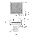
- FIG.1 (a) is a top view which shows the structure of the one aspect
- FIG.1 (b) is a cross-sectional side view explaining the usage aspect.
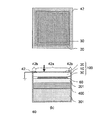
- FIG. 2A is a plan view showing a configuration of one aspect of the touch panel of the present invention
- FIG. 2B is a cross-sectional side view illustrating the usage aspect.
- FIG. 3A is a plan view showing a configuration of one aspect of the electronic device of the present invention
- FIG. 3B is a cross-sectional side view illustrating the usage.
- FIG. 11 is a perspective view illustrating a configuration of one embodiment of an electronic apparatus according to the invention. It is sectional drawing explaining the part of the touchscreen and electronic device of this invention. It is sectional drawing explaining the part of the touchscreen and electronic device of this invention. It is sectional drawing explaining the part of the touchscreen and electronic device of this invention.
- the transparent piezoelectric sheet with frame of the present embodiment includes one transparent piezoelectric film 10 containing an organic polymer, and one first transparent flat plate disposed on the first main surface of the transparent piezoelectric film 10.
- the second transparent flat plate electrode 30 has a second transparent flat plate electrode portion 30a, and the outline of the second transparent flat plate electrode portion 30a is inside the outline of the first transparent flat plate electrode portion 20a in plan view.
- the transparent piezoelectric sheet with a frame of this embodiment will be described.
- the arrow in a figure shows a touch direction.
- the transparent piezoelectric sheet with frame of the present embodiment includes a transparent piezoelectric sheet 100 and a frame 40.
- the transparent piezoelectric sheet 100 includes one transparent piezoelectric film 10, one first transparent flat plate electrode 20, and one second transparent flat plate electrode 30.
- FIG. 1A is a plan view seen from the second transparent flat plate electrode 30 side.
- the transparent piezoelectric film 10 is not particularly limited as long as it contains an organic polymer and has piezoelectricity and transparency.
- the transparent piezoelectric film 10 is particularly preferably a film formed from a polymer such as vinylidene fluoride-tetrafluoroethylene copolymer, vinylidene fluoride-trifluoroethylene copolymer, or polyvinylidene fluoride.
- a film formed from a vinylidene fluoride-tetrafluoroethylene copolymer is preferable.
- the vinylidene fluoride: tetrafluoroethylene (molar ratio) in the vinylidene fluoride-tetrafluoroethylene copolymer is preferably 50:50 to 90:10 from the viewpoint of piezoelectricity related to the detection sensitivity of touch pressure, and 65 : 35 to 80:20 is more preferable.
- stretched may be used.
- the transparent piezoelectric film 10 may contain an additive added to the resin film as long as the piezoelectricity and transparency are not impaired.
- the thickness of the transparent piezoelectric film 10 is usually 1 ⁇ m to 200 ⁇ m, preferably 50 ⁇ m or less from the viewpoint of transparency, and preferably 20 ⁇ m to 100 ⁇ m from the viewpoint of touch pressure detection sensitivity.
- the transparent piezoelectric film 10 may be a single film or a plurality of films.
- the transparent piezoelectric film 10 preferably has a quadrangular shape.
- the first transparent flat plate electrode 20 is disposed on the first main surface of the transparent piezoelectric film 10. As shown in FIG. 1, the first transparent flat plate electrode 20 has at least a first transparent flat plate electrode portion 20a, and preferably further has a first lead portion 20b.
- the first lead portion 20 b makes it easy to connect the first transparent flat plate electrode 20 to the detection circuit 300 via the electric wire 70.
- the 1st transparent flat plate electrode 20 should just have transparency.
- the first transparent flat plate electrode 20 for example, an electrode selected from inorganic electrodes such as ITO (indium tin oxide) and tin oxide, and conductive polymers such as thiophene conductive polymer, polyaniline, and polypyrrole is used. be able to.
- the second transparent flat plate electrode 30 is disposed on the second main surface of the transparent piezoelectric film 10, that is, the surface opposite to the first main surface on which the first transparent flat plate electrode 20 is disposed. As shown in FIG. 1, the second transparent flat plate electrode 30 has at least a second transparent flat plate electrode portion 30a, and preferably further has a second lead portion 30b. The second lead portion 30 b makes it easy to connect the second transparent flat plate electrode 30 to the detection circuit 300 via the electric wire 70.
- the outline of the second transparent flat plate electrode portion 30a is located inside the outline of the first transparent flat plate electrode portion 20a in plan view.
- the ratio of the area of the second transparent flat plate electrode portion to the area of the main surface of the transparent piezoelectric film is preferably 70% or more.
- the area of the second transparent flat plate electrode part is equal to the effective area of touch pressure detection.
- the second transparent flat plate electrode 30 an electrode similar to the first transparent flat plate electrode 20 can be used.
- the surface of the first transparent flat plate electrode 20 and / or the second transparent flat plate electrode 30 is a resin sheet having flexibility such as a polyethylene terephthalate sheet in order to protect them. It may be covered with a protective layer.
- the protective layer may also serve as an insulating layer.
- the frame 40 covers the periphery of the transparent piezoelectric sheet 100 in a frame shape.
- the frame 40 is provided with a groove and a hole through which the first lead portion 20b and the second lead portion 30b pass. Or you may connect with external wiring by comprising a part of flame
- the first transparent flat plate electrode portion 20 a is disposed such that its outline completely overlaps the frame 40 in plan view.
- the second transparent flat plate electrode portion 30a is disposed such that its outline does not overlap the frame 40 at all in a plan view.
- the transparent piezoelectric sheet of the present embodiment can be manufactured, for example, by a manufacturing method including the following steps.
- the step of laminating the second transparent flat plate electrode 30 on a part of the second main surface of the transparent piezoelectric film 10 (4)
- a transparent film is formed from the above-described polymer by a conventional method.
- Such a film may be obtained as a commercial product.
- the film may be subjected to a stretching treatment from the viewpoint of improving piezoelectricity.
- the stretching is preferably 3 to 10 times in the uniaxial direction.
- the stretching process may be performed by a conventional method.
- the method of imparting piezoelectricity to the film differs depending on the polymer constituting the film, but from vinylidene fluoride-tetrafluoroethylene copolymer, vinylidene fluoride-trifluoroethylene copolymer, or polyvinylidene fluoride.
- polarization treatment also referred to as poling treatment
- the polarization treatment can be performed by a corona discharge treatment or a conventional method.
- the film is sandwiched from both sides with a metal electrode or the like, and a DC electric field of 30 to 400 MV / m is applied for 0.1 seconds to 60 minutes.
- the first transparent flat plate electrode 20 is laminated on the first main surface of the transparent piezoelectric film 10.
- the first transparent flat plate electrode 20 can be laminated by forming it on the surface of the transparent piezoelectric film 10 by sputtering or vapor deposition, for example.
- a resin sheet eg, a polyethylene terephthalate sheet (PET sheet)
- PET sheet polyethylene terephthalate sheet
- the first transparent flat plate electrode 20 is preferably adjacent to the transparent piezoelectric film 10, but as long as a piezoelectric signal can be detected, the first transparent flat plate electrode 20 and the transparent piezoelectric film 10 are transparently bonded. You may bond together with an agent (for example, epoxy adhesive).
- the first transparent flat plate electrode portion 20a and the first lead portion 20b can be integrally formed.
- the second transparent flat plate electrode 30 may be laminated in the same manner using the same electrode as the first transparent flat plate electrode 20.
- the second transparent flat plate electrode portion 30a and the second lead portion 30b can be integrally formed.
- Step (4) may be performed by a conventional method depending on the form of the frame 40.
- the material of the frame 40 is not particularly limited, but is preferably made of resin.
- the touch position detection touch panel 200 is disposed on the surface opposite to the touch side of the transparent piezoelectric sheet 100.
- the touch position detecting touch panel 200 is in contact with the transparent piezoelectric sheet 100 through the insulating layer 60.
- the transparent piezoelectric sheet 100 can be used by being attached to one surface of the touch position detecting touch panel 200 by the adhesive portion 50.
- An electric signal generated by pushing the overlapping area of the first transparent flat plate electrode 20 and the second transparent flat plate electrode 30 as shown by the arrow in FIG. 1B is transmitted to the detection circuit 300 through the electric wire 70 and pressed. (Touch pressure) is detected. Since the transparent piezoelectric sheet 100 has flexibility, the touch position detection touch panel 200 also receives touch pressure through the insulating layer 60 at the same time. Accordingly, the touch position is also detected by the touch position detection touch panel 200.
- the first transparent flat plate electrode portion 20a is disposed such that its outline completely overlaps the frame 40 in plan view. Since the direction of this planar view is usually almost the same as the direction in which the user views the transparent piezoelectric sheet with frame of the present embodiment when touched, the outline of the first transparent flat plate electrode portion is visible to the user. Absent. For this reason, since two contour lines do not exist in the very near position, these contour lines do not unnecessarily attract the user's attention.
- the transparent piezoelectric sheet 100 can be used by being attached to the display surface of the display device by the adhesive portion 50. Since the transparent piezoelectric sheet 100 can detect a touch pressure, the transparent piezoelectric sheet with a frame of this embodiment can be used for touch pressure detection.
- the touch panel of the present embodiment includes one transparent piezoelectric film 10 containing an organic polymer, one first transparent flat plate electrode 20 disposed on the first main surface of the transparent piezoelectric film 10, The second transparent flat plate electrode 30 disposed on the second main surface of the transparent piezoelectric film 10, and the first transparent flat plate electrode 20 has a first transparent flat plate electrode portion 20a, and The second transparent flat plate electrode 30 has a second transparent flat plate electrode portion 30a, and the outline of the first transparent flat plate electrode portion 20a is located inside the outline of the second transparent flat plate electrode portion 30a in plan view.
- the outline of the first transparent flat plate electrode portion 20a completely overlaps the frame 41, and the outline of the second transparent flat plate electrode portion 30a does not overlap the frame 41 at all. To do.
- the touch panel of this embodiment includes a transparent piezoelectric sheet 100, a frame 41, an insulating layer 60, and a touch position detection touch panel 201.
- the transparent piezoelectric sheet 100 includes one transparent piezoelectric film 10, one first transparent flat plate electrode 20, and one second transparent flat plate electrode 30.
- the transparent piezoelectric film 10, the first transparent flat plate electrode 20, and the second transparent flat plate electrode 30 have the same meaning as described in the first embodiment.
- FIG. 2A is a plan view seen from the first transparent flat plate electrode 20 side.
- the first transparent flat plate electrode 20 is disposed on the touch-side surface of the transparent piezoelectric sheet 100 and is a ground electrode.
- the touch position detection touch panel 201 is disposed on the surface opposite to the touch side of the transparent piezoelectric sheet 100 so as to be in contact with the transparent piezoelectric sheet 100 via the insulating layer 60.
- the touch position detecting touch panel 201 is not particularly limited, and any conventionally used touch position detecting touch panel such as a resistive film type, a capacitance type, an ultrasonic type, and an optical type is used. Can be used. Since the transparent piezoelectric sheet 100 has flexibility, an electric signal generated by pressing as shown by an arrow in FIG. 2B is transmitted to the detection circuit 300 through the electric wire 70, and the pressing (touch pressure) is detected. The Since the transparent piezoelectric sheet 100 has flexibility, the touch position detecting touch panel 201 also receives touch pressure through the insulating layer 60 at the same time. Accordingly, the touch position is also detected by the touch position detection touch panel 201.
- the frame 41 covers the peripheral portions of the transparent piezoelectric sheet 100 and the touch position detection touch panel 201 in a frame shape.
- the frame 41 is provided with grooves and holes through which the first lead portion 20b and the second lead portion 30b pass.
- a part of the frame 41 with a conductive material such as a metal, a part or all of these lead parts may be replaced with the part.
- the first transparent flat plate electrode portion 20 a is disposed so that its outline completely overlaps the frame 41 in plan view.
- the second transparent flat plate electrode portion 30a is arranged such that its outline does not overlap the frame 41 at all in a plan view.
- the surface of the first transparent flat plate electrode 20 and / or the second transparent flat plate electrode 30 is a resin sheet having flexibility such as a polyethylene terephthalate sheet in order to protect them. It may be covered with a protective layer. The protective layer may also serve as an insulating layer. Since the transparent piezoelectric sheet 100 can detect touch pressure, the touch panel of this embodiment can be used for touch pressure and touch position detection.
- the electronic device of the present embodiment includes one transparent piezoelectric film 10 containing an organic polymer, one first transparent flat plate electrode 20 disposed on the first main surface of the transparent piezoelectric film 10, and , One second transparent flat plate electrode 30 disposed on the second main surface of the transparent piezoelectric film 10, and the first transparent flat plate electrode 20 has a first transparent flat plate electrode portion 20a,
- the second transparent flat plate electrode 30 has a second transparent flat plate electrode portion 30a, and the outline of the second transparent flat plate electrode portion 30a is located inside the outline of the first transparent flat plate electrode portion 20a in plan view.
- the housing has an opening 42a, and the outline of the first transparent flat plate electrode portion 20a in plan view. Is completely overlapped with the inner edge 42b that defines the opening 42a. And the outline of the second transparent plate electrode portion 30a does not overlap at all on the inner edge 42b.
- the electronic apparatus of this embodiment includes a transparent piezoelectric sheet 100, a housing 42, an insulating layer 60, a touch position detection touch panel 201, a display device 400, and a detection circuit 301.
- the first transparent flat plate electrode 20 and the second transparent flat plate electrode 30 are connected to the detection circuit 301 by electric wires, respectively.
- the transparent piezoelectric sheet 100 includes one transparent piezoelectric film 10, one first transparent flat plate electrode 20, and one second transparent flat plate electrode 30.
- the first transparent flat plate electrode 20 is disposed on the first main surface of the transparent piezoelectric film 10.
- the second transparent flat plate electrode 30 is disposed on the second main surface of the transparent piezoelectric film 10.
- the outline of the second transparent flat plate electrode portion 30a is located inside the outline of the first transparent flat plate electrode portion 20a in plan view, as in the case of the transparent piezoelectric sheet 100 of FIG.
- the transparent piezoelectric film 10, the first transparent flat plate electrode 20, the second transparent flat plate electrode 30, the insulating layer 60, and the touch position detection touch panel 201 are the same as those described in the second embodiment (touch panel). It represents the same meaning.
- the touch position detection touch panel 201 is disposed on the surface opposite to the touch side of the transparent piezoelectric sheet 100 so as to be in contact with the transparent piezoelectric sheet 100 via the insulating layer 60. Yes. That is, the electronic device of the present embodiment corresponds to a device using the transparent piezoelectric sheet 100 and the touch position detection touch panel 201 in the second embodiment (touch panel) as members of an electronic device.
- the first transparent flat plate electrode 20 is composed of a first transparent flat plate electrode portion 20a
- the second transparent flat plate electrode 30 is composed of a second transparent flat plate electrode portion 30a.
- the first transparent flat plate electrode 20 is disposed on the touch-side surface of the transparent piezoelectric sheet 100 and is a ground electrode.
- the surface of the first transparent flat plate electrode 20 and / or the second transparent flat plate electrode 30 is a resin sheet having flexibility such as a polyethylene terephthalate sheet in order to protect them. It may be covered with a protective layer.
- the protective layer may also serve as an insulating layer.
- the housing 42 has an opening 42a and an inner edge 42b that defines the opening 42a.
- the outline of the first transparent flat plate electrode portion 20a completely overlaps the inner edge portion 42b that defines the opening 42a.
- the contour of the second transparent flat plate electrode portion 30a does not overlap the inner edge portion 42b at all.
- the touch position detecting touch panel 201 also receives touch pressure through the insulating layer 60 at the same time. Accordingly, the touch position is also detected by the touch position detection touch panel 201, and based on this, the operation is performed as set in advance. As is clear from the above description, the operation of the electronic device by such a touch is performed in the opening 42a.
- FIG. 4 shows a schematic diagram when such an electronic device is a mobile phone.
- the mobile phone includes a housing 43 having an opening 43a and an inner edge 43b that defines the opening 43a.
- the transparent piezoelectric sheet 100 is disposed so as to be covered in a frame shape on the inner edge portion 43b.
- the touch panel and electronic device of this modification are demonstrated.
- the touch position detection touch panel 201 is disposed on the surface of the transparent piezoelectric sheet 100 opposite to the touch side.
- the transparent piezoelectric sheet 100 is disposed on the touch side surface.
- the touch position detection touch panel 201 is in direct contact with the transparent piezoelectric sheet 100.
- the first transparent flat plate electrode 20 of the transparent piezoelectric sheet 100 is a ground electrode disposed on the touch side surface of the transparent piezoelectric film 10, and also serves as a ground electrode of the touch position detection touch panel 201.
- the touch panel and the electronic device of the present modification Due to the simplification of the structure, the touch panel and the electronic device of the present modification have a low manufacturing cost.
- FIG. 5 for explaining the touch panel and the electronic device of this modification only the touch position detecting touch panel 201 and the transparent piezoelectric sheet 100 are shown, but the other parts are the second embodiment (touch panel) and the third embodiment. This is the same as the embodiment (electronic device).
- the touch position indicated by the arrow in FIG. 5 is detected by the touch position detection touch panel 201, and the touch pressure is detected by the transparent piezoelectric sheet 100.
- the touch panel and electronic device of this modification are demonstrated.
- the touch position detection touch panel 201 is disposed on the touch-side surface of the transparent piezoelectric sheet 100 as in the second modification.
- the second transparent flat plate electrode 30 of the transparent piezoelectric sheet 100 is disposed on the surface opposite to the touch side and is a ground electrode.
- the ground electrode is disposed on the side opposite to the touch side, the noise of the output voltage is reduced in the touch panel and the electronic device of the present modification.
- the touch position indicated by the arrow in FIG. 6 is detected by the touch position detection touch panel 201, and the touch pressure is detected by the transparent piezoelectric sheet 100.
- the touch panel and electronic device of this modification are demonstrated.
- the touch position detection touch panel 201 is disposed on the surface of the transparent piezoelectric sheet 100 opposite to the touch side.
- the second transparent flat plate electrode 30 of the transparent piezoelectric sheet 100 is disposed on the surface opposite to the touch side and is a ground electrode.
- a ground electrode 80 is disposed on the touch-side surface of the transparent piezoelectric sheet 100 with an insulating layer 60 interposed therebetween.
- the ground electrodes are arranged on both main surfaces of the transparent piezoelectric sheet 100, the noise of the output voltage is particularly reduced in the touch panel and the electronic device of this modification.
- the touch pressure indicated by the arrow in FIG. 7 is detected by the transparent piezoelectric sheet 100, and the touch position is detected by the touch position detection touch panel 201.
- the transparent piezoelectric sheet of the present invention can be used for a touch panel or the like.
Landscapes
- Engineering & Computer Science (AREA)
- General Engineering & Computer Science (AREA)
- Physics & Mathematics (AREA)
- General Physics & Mathematics (AREA)
- Theoretical Computer Science (AREA)
- Human Computer Interaction (AREA)
- Position Input By Displaying (AREA)
Abstract
Description
これまでに実用化されているタッチパネルでは、ユーザーが押した位置(本明細書中、タッチ位置と称する場合がある)を検出できるのみであり、ユーザーが押した強さ(すなわち、押圧の高さ(強さ)。本明細書中、タッチ圧と称する場合がある)を検出する事はできなかった。一方、タッチパネルを用いた表示および入力装置において、タッチパネルは表示装置の前面に設置するので、表示装置の表示の視認性を高めるため、タッチパネルの透明性が高いことが求められる。
また、特許文献2には、タッチスクリーンに結合し、前記タッチスクリーンの各接触に対する位置座標の組を決定する第1センサシステムと、前記タッチスクリーンに結合し、第1タイプの物体により、前記タッチスクリーンの各接触を確認し、第2タイプの物体により、前記タッチスクリーンの各接触を無効にする、前記位置座標の組を決定する能力はない第2センサシステムとを含んでいるタッチスクリーンシステムが開示され、かつ第1センサシステムとして具体的には、LCDの視覚領域の外側に配置された力センサが開示されている。
このようなタッチ圧検出用の透明圧電シートは、好ましくは、タッチ位置検出用のタッチパネルと組み合わせて使用される。この際、タッチ圧検出用の透明圧電シートは、平面視における大きさが、タッチ位置検出用のタッチパネルの大きさを超えないことが好ましく、一方、タッチ位置検出用のタッチパネルの検出有効領域の全領域においてタッチ圧を検出できることが望まれる。タッチ位置検出用のタッチパネルの面積における検出有効領域の面積の比率が高いことが、常に求められていることは一般に知られていることであるが、タッチ位置検出用のタッチパネルの検出有効領域の全領域においてタッチ圧を検出できるようにするには、必然的に、タッチ圧検出用の透明圧電シートに対して、タッチ位置検出用のタッチパネルよりも更に厳しい要求が課せられることになる。
しかし、タッチ圧検出用の透明圧電シートは、取り扱い易さ等の観点から、その周辺部をフレームで覆うことが好ましい。
この場合、タッチ圧検出用の透明圧電シートの全面で、タッチ圧検出が可能であると、透明圧電シートは、フレームによって加わる圧力を検出していまい、本来目的とするタッチ圧の検出が不可能になるか、あるいはその精度を著しく低下させる。
また、タッチ圧検出用の透明圧電シートは、フレームに収納せずに、そのまま電子装置の部材として、開口部を有する筐体内に配置されて用いられる場合もある。この場合も、前記開口部を画定する筐体の内縁部がタッチ圧検出用の透明圧電シートに接触していると、フレームの場合と同様に、透明圧電シートは、内縁部によって加わる圧力を検出していまい、本来目的とするタッチ圧の検出が不可能になるか、あるいはその精度を著しく低下させる。
また、透明平板電極の輪郭は、本来はほとんど目立たないが、透明圧電体膜の両面の各透明平板電極の輪郭が少しずれた場合には、非常に近い位置に輪郭線が2本存在することになるので、予想以上に目立つようになり、外観に劣り、使用者の不必要な注意を引いてしまう。
なお、上述の公知のタッチパネルおよび圧電センサはいずれも、タッチ位置検出用のタッチパネルと組み合わせて使用することを目的とするものではないので、これらには、このような問題は無い。
また、前記第2透明平板電極部の輪郭が、平面視において前記第1透明平板電極部の輪郭の内側に位置しさえすればよいので、第1透明平板電極部と第2透明平板電極部との位置関係が若干ずれても、製品の性能に影響を与えることがない。このことにより、製造時の不良品率を下げることができ、製造コストを低くできる。
ここで、前記第2透明平板電極部の輪郭が、平面視において、当該フレームに全く重ならないことにより、必然的に、フレームによる圧力は、電気信号として検出回路に伝わらないので、タッチ圧の検出を妨げない。
当該比は、より好ましくは90%以上100%未満、更に好ましくは95%以上100%未満である。
前記第2透明平板電極部の面積は、通常、タッチ圧検出の有効面積に等しいので、これにより、十分な有効面積が得られる。
ことを特徴とする。
これにより、例えばタッチ位置検出用タッチパネルと組み合わせて用いる場合でも、タッチ位置検出用タッチパネルによるタッチ位置の検出の感度および精度を損なうことなく、高感度および高精度にタッチ圧を検出する機能を付与することができる。この厚さは、透明性の観点から好ましくは50μm以下であり、タッチ圧の検出感度の観点から好ましくは、20μm~100μmである。
第1リード部、および第2リード部は、それぞれ、第1透明平板電極部と第2透明平板電極部とを、検出回路等の外部の配線とを繋ぐものである。これにより、外部の配線への接続が容易になる。
ここで、前記フレームは、好ましくは、リード部を通すための、溝および/または穴を有する。あるいは、フレームの一部を金属等の導電性材料で構成することにより、外部の配線と接続してもよい。
これにより、フレーム付透明圧電シートをタッチ位置検出用タッチパネル等の任意の物体に貼付して用いることができ、その表面にタッチ圧を検出する機能を付与することができる。
ここで、当該粘着部は、例えば、フレーム表面上に設けることができる。
また、当該粘着部は、使用時に使用者から見えない位置に設けられていることが好ましい。
当該フレーム付透明圧電シートはタッチ圧を検出できるので、これにより、タッチ位置検出用タッチパネルに、タッチ圧を検出する機能を付与することができる。
前記タッチ位置検出用タッチパネルは、通常、前記フレーム付透明圧電シートのタッチ側の面またはタッチ側とは反対側の面のいずれかに配置される。
但し、前記フレーム付透明圧電シートの、タッチ位置検出用タッチパネル側の電極がグランド電極であり、かつ、タッチ位置検出用タッチパネルの、フレーム付透明圧電シート側の電極もまたグランド電極である場合は、これらの2つの電極は接触していてもよい。
当該フレーム付透明圧電シートは、製造コストが低いという抵抗膜式タッチ位置検出用タッチパネルの有利な特性または多点検知が容易であるという静電容量式のタッチ位置検出用タッチパネルの有利な特性を損なうことなく、これらにタッチ圧を検出する機能を付与することができる。
当該タッチパネルは、タッチの圧および位置の両方を検出することができる。
前記タッチ位置検出用タッチパネルは、通常、前記フレーム付透明圧電シートのタッチ側の面またはタッチ側とは反対側の面のいずれかに配置される。
この際、前記フレーム付透明圧電シートの、タッチ位置検出用タッチパネル側の電極は、通常、タッチ位置検出用タッチパネルの電極と電気的に接しないように配置される。具体的には例えば、これらの電極間に、これらに隣接するように、絶縁層が配置される。当該絶縁層は、好ましくは可撓性を有する。
但し、前記フレーム付透明圧電シートの、タッチ位置検出用タッチパネル側の電極がグランド電極であり、かつ、タッチ位置検出用タッチパネルの、フレーム付透明圧電シート側の電極もまたグランド電極である場合は、これらの2つの電極は接触していてもよい。
上述の第1観点に係るフレーム付透明圧電シートについて説明したのと同様に、前記第2透明平板電極部の輪郭が、平面視において前記第1透明平板電極部の輪郭の内側に位置することにより、タッチ圧検出用圧電シートによって検出されるタッチ圧の検出領域とタッチ位置検出用タッチパネルによって検出されるタッチ位置の検出領域とを、高度に一致させることが可能となる。
また、上述の第1観点に係るフレーム付透明圧電シートについて説明したのと同様に、製造時の不良品率を下げることができ、製造コストを低くできる。
また、上述の第1観点に係るフレーム付透明圧電シートについて説明したのと同様に、外観に優れる。
前記タッチ位置検出用タッチパネルは、通常、前記フレーム付透明圧電シートのタッチ側の面またはタッチ側とは反対側の面のいずれかに配置される。
この際、前記透明圧電シートの、タッチ位置検出用タッチパネル側の電極は、通常、タッチ位置検出用タッチパネルの電極と電気的に接しないように配置される。具体的には例えば、これらの電極間に、これらに隣接するように、絶縁層が配置される。当該絶縁層は、好ましくは可撓性を有する。
但し、前記透明圧電シートの、タッチ位置検出用タッチパネル側の電極がグランド電極であり、かつ、タッチ位置検出用タッチパネルの、透明圧電シート側の電極もまたグランド電極である場合は、これらの2つの電極は接触していてもよい。
これにより、出力電圧のノイズを軽減することができる。
これにより、当該タッチパネルの構造を簡略化し、製造コストを下げることができる。
また、上述の第1観点に係るフレーム付透明圧電シートについて説明したのと同様に、外観に優れる。
前記筐体が、開口部を有し、平面視において、前記第1透明平板電極部の輪郭が、前記開口部を画定する内縁部に完全に重なり、かつ前記第2透明平板電極部の輪郭は、当該内縁部に全く重ならないことにより、必然的に、内縁部による圧力は、電気信号として検出回路に伝わらないので、タッチ圧の検出を妨げない。
これにより、当該タッチパネルは、タッチの圧および位置の両方を検出することができる。
また、上述の第1観点に係るフレーム付透明圧電シートについて説明したのと同様に、タッチ圧検出用圧電シートによって検出されるタッチ圧の検出領域とタッチ位置検出用タッチパネルによって検出されるタッチ位置の検出領域とが、高度に一致している。
ここで、タッチ位置検出用タッチパネルとしては、特に限定されず、従来使用されているタッチ位置検出用タッチパネルを用いることができる。
これにより、出力電圧のノイズを軽減することができる。
これにより、当該タッチパネルの構造を簡略化し、製造コストを下げることができる。
本明細書中、「共重合体」なる用語は、特に限定の無い限り、ランダム共重合体、ブロック共重合体、およびグラフト共重合体等を包含することを意図して用いられる。
本明細書中、「透明」なる用語は、光透過性を有すること、より具体的には、ASTM D1003に記載の方法に準じた方法で測定した全光線透過率が40%以上であることを意味する。
まず、本実施形態の透明圧電シートの構成について説明する。
本実施形態のフレーム付透明圧電シートは、1個の、有機重合体を含有する透明圧電体膜10と、当該透明圧電体膜10の第1主面に配置された1個の第1透明平板電極20と、当該透明圧電体膜10の第2主面に配置された1個の第2透明平板電極30と、からなり、前記第1透明平板電極20は、第1透明平板電極部20aを有し、前記第2透明平板電極30は、第2透明平板電極部30aを有し、前記第2透明平板電極部30aの輪郭が、平面視において前記第1透明平板電極部20aの輪郭の内側に位置する透明圧電シート100と、前記透明圧電シート100の周縁部を覆うフレーム40とを含み、平面視において、前記第1透明平板電極部20aの輪郭が、前記フレーム40に完全に重なり、かつ前記第2透明平板電極部30aの輪郭は、当該フレーム40に全く重ならないことを特徴とする。
図1に示されるように、本実施形態のフレーム付透明圧電シートは、透明圧電シート100とフレーム40とを備える。
透明圧電シート100は、1個の透明圧電体膜10と、1個の第1透明平板電極20と、1個の第2透明平板電極30とを備える。
なお、図1(a)は、第2透明平板電極30の側から見た平面図である。
透明圧電体膜10は、有機重合体を含有し、圧電性および透明性を有するものであれば、特に限定されない。当該有機重合体としては、フッ化ビニリデン-テトラフルオロエチレン共重合体、フッ化ビニリデン-トリフルオロエチレン共重合体、ポリフッ化ビニリデンが挙げられる。透明圧電体膜10として特に好ましくは、フッ化ビニリデン-テトラフルオロエチレン共重合体、フッ化ビニリデン-トリフルオロエチレン共重合体、ポリフッ化ビニリデン等のポリマーから形成される膜が挙げられる。
フッ化ビニリデン-テトラフルオロエチレン共重合体における、フッ化ビニリデン:テトラフルオロエチレン(モル比)は、タッチ圧の検出感度に関係する圧電性の観点から、50:50~90:10が好ましく、65:35~80:20がより好ましい。
フッ化ビニリデン-テトラフルオロエチレン共重合体から形成される膜、フッ化ビニリデン-トリフルオロエチレン共重合体から形成される膜、およびポリフッ化ビニリデンから形成される膜は、圧電性向上の観点から、延伸処理したものであってもよい。
透明圧電体膜10は、その圧電性および透明性を害さない範囲で、樹脂フィルムに添加される添加剤を含有してもよい。
透明圧電体膜10は、単一膜であってもよく、複数の膜からなってもよい。
透明圧電体膜10は、好ましくは4角形形状である。
第1透明平板電極20は、透明圧電体膜10の第1主面に配置されている。
図1に示されるように、前記第1透明平板電極20は、少なくとも第1透明平板電極部20aを有し、好ましくは更に第1リード部20bを有する。第1リード部20bは、第1透明平板電極20を、電線70を介して、検出回路300に接続することを容易にする。
第2透明平板電極30は、透明圧電体膜10の第2主面、すなわち、第1透明平板電極20が配置されている第1主面とは反対側の面上に配置されている。
図1に示されるように、第2透明平板電極30は、少なくとも第2透明平板電極部30aを有し、好ましくは更に第2リード部30bを有する。第2リード部30bは、第2透明平板電極30を、電線70を介して、検出回路300に接続することを容易にする。
前記第2透明平板電極部30aの輪郭は、平面視において前記第1透明平板電極部20aの輪郭の内側に位置する。
第2透明平板電極30としては、第1透明平板電極20と同様の電極を用いることができる。
なお、所望により、第1透明平板電極20および/または第2透明平板電極30の表面(特にタッチされる表面)は、これらを保護するために、ポリエチレンテレフタレートシート等の可撓性を有する樹脂シート等の保護層で覆われていてもよい。当該保護層は、絶縁層を兼ねていてもよい。
フレーム40は、前記透明圧電シート100の周縁部を額縁状に覆っている。図には示されていないが、フレーム40には、第1リード部20bおよび第2リード部30bを通す溝及び穴が設けられている。あるいは、フレーム40の一部を金属等の導電性材料で構成することにより、外部の配線と接続してもよい。
これにより、フレームによる圧力は、電気信号として検出回路に伝わらないので、タッチ圧の検出を妨げず、かつ、本実施態様のフレーム付透明圧電シートは、外観に優れる。
フレーム40の表面上には、粘着部50が設けられている。
これにより、本実施態様のフレーム付透明圧電シートを、タッチ位置検出用タッチパネルおよび/またはディスプレイに貼り付けて、使用することができる。
次に、本実施形態のフレーム付透明圧電シートの製造方法について説明する。
(1)有機重合体を含有し、主面全体が圧電性を有する透明圧電体膜10を用意する工程
(2)透明圧電体膜10の第1主面の一部に第1透明平板電極20を積層する工程
(3)透明圧電体膜10の第2主面の一部に第2透明平板電極30を積層する工程
(4)工程(1)~(3)で得られた透明圧電シートを、フレーム40に収容する工程
工程(1)においては、上記のようなポリマーから慣用の用法で、透明膜を形成される。このような膜は、市販品にて入手してもよい。
当該膜は、所望により、圧電性向上の観点から、延伸処理を行ってもよい。ここで、延伸は、一軸方向の3~10倍延伸が好ましい。当該延伸処理は、慣用の方法によって行えばよい。
当該分極処理は、コロナ放電処理、または慣用の方法によって行うことができる。例えば、フィルムの両面から金属電極等で挟み込み、30~400MV/mの直流電界、0.1秒~60分間、の印加を実施する。
工程(2)においては、透明圧電体膜10の第1主面に第1透明平板電極20を積層する。第1透明平板電極20は、例えば、透明圧電体膜10の面上にスパッタ法または蒸着法などにより形成することにより、積層することができる。
第1透明平板電極部20aおよび第1リード部20bは、一体として形成することができる。
工程(3)において、第2透明平板電極30は、第1透明平板電極20と同様の電極を用い、同様に積層すればよい。
第2透明平板電極部30aおよび第2リード部30bは、一体として形成することができる。
次に、図1(b)を参照して、本実施形態のフレーム付透明圧電シートの使用について説明する。
図1(b)において、タッチ位置検出用タッチパネル200は、透明圧電シート100のタッチ側とは反対側の面に配置されている。タッチ位置検出用タッチパネル200は、絶縁層60を介して透明圧電シート100に接触している。
透明圧電シート100は、粘着部50によって、タッチ位置検出用タッチパネル200の一方の面に貼付して用いることができる。
第1透明平板電極20と前記第2透明平板電極30との重複領域を、図1(b)の矢印に示すように押すことによって生じた電気信号は、電線70を通じて検出回路300に伝わり、押圧(タッチ圧)が検出される。透明圧電シート100は、可撓性を有するので、絶縁層60を介して、タッチ位置検出用タッチパネル200もまた同時にタッチの圧力を受ける。これによってタッチ位置もまた、タッチ位置検出用タッチパネル200によって、検出される。
この平面視の方向は、通常、使用者がタッチ時に、本実施形態のフレーム付透明圧電シートを見る方向と、ほぼ同一になるので、使用者からは、第1透明平板電極部の輪郭は見えない。このため、非常に近い位置に輪郭線が2本存在することがないので、これらの輪郭線が不必要に使用者の注意を引くことがない。
また、これに換えて、透明圧電シート100は、粘着部50によって、ディスプレイ装置のディスプレイ面に貼付して用いることもできる。
透明圧電シート100はタッチ圧を検出できるので、本実施態様のフレーム付透明圧電シートは、タッチ圧検出用に用いることができる。
まず、本実施形態のタッチパネルの構成について説明する。
本実施形態のタッチパネルは、1個の、有機重合体を含有する透明圧電体膜10と、当該透明圧電体膜10の第1主面に配置された1個の第1透明平板電極20と、当該透明圧電体膜10の第2主面に配置された1個の第2透明平板電極30と、からなり、前記第1透明平板電極20は、第1透明平板電極部20aを有し、前記第2透明平板電極30は、第2透明平板電極部30aを有し、前記第1透明平板電極部20aの輪郭が、平面視において前記第2透明平板電極部30aの輪郭の内側に位置する透明圧電シート100と、当該透明圧電シート100の第1主面に配置されたタッチ位置検出用タッチパネル201と、前記透明圧電シート100の周縁部および前記タッチ位置検出用タッチパネル201の周縁部を覆うフレーム41とを含み、平面視において、前記第1透明平板電極部20aの輪郭が、前記フレーム41に完全に重なり、かつ前記第2透明平板電極部30aの輪郭は、当該フレーム41に全く重ならないことを特徴とする。
図2に示されるように、本実施形態のタッチパネルは、透明圧電シート100と、フレーム41と、絶縁層60と、タッチ位置検出用タッチパネル201とを備える。透明圧電シート100は、1個の透明圧電体膜10と、1個の第1透明平板電極20と、1個の第2透明平板電極30とから構成される。
ここで、透明圧電体膜10、第1透明平板電極20、および第2透明平板電極30は、それぞれ前記第1実施形態で説明したものと、同様の意味を表す。
なお、図2(a)は、第1透明平板電極20の側から見た平面図である。
図2(b)において、第1透明平板電極20は、透明圧電シート100のタッチ側の面に配置されており、かつ、グランド電極である。
ここで、タッチ位置検出用タッチパネル201としては、特に限定されず、従来使用されている、抵抗膜式、静電容量式、超音波式、および光学式等の任意の形式のタッチ位置検出用タッチパネルを用いることができる。
透明圧電シート100は、可撓性を有するので、図2(b)の矢印に示すように押すことによって生じた電気信号は、電線70を通じて検出回路300に伝わり、押圧(タッチ圧)が検出される。透明圧電シート100は、可撓性を有するので、タッチ位置検出用タッチパネル201もまた同時に絶縁層60を介してタッチの圧力を受ける。これによってタッチ位置もまた、タッチ位置検出用タッチパネル201によって、検出される。
図2に示されるように、前記第1透明平板電極部20aは、その輪郭が、平面視において、前記フレーム41に完全に重なるように配置される。一方、前記第2透明平板電極部30aは、その輪郭が、平面視において、当該フレーム41に全く重ならないように配置される。
なお、所望により、第1透明平板電極20および/または第2透明平板電極30の表面(特にタッチされる表面)は、これらを保護するために、ポリエチレンテレフタレートシート等の可撓性を有する樹脂シート等の保護層で覆われていてもよい。当該保護層は、絶縁層を兼ねていてもよい。
透明圧電シート100はタッチ圧を検出できるので、本実施形態のタッチパネルは、タッチ圧およびタッチ位置検出用に用いることができる。
まず、本実施形態の電子機器の構成について説明する。
本実施形態の電子機器は、有機重合体を含有する、1個の透明圧電体膜10と、当該透明圧電体膜10の第1主面に配置された1個の第1透明平板電極20と、当該透明圧電体膜10の第2主面に配置された1個の第2透明平板電極30と、からなり、前記第1透明平板電極20は、第1透明平板電極部20aを有し、前記第2透明平板電極30は、第2透明平板電極部30aを有し、前記第2透明平板電極部30aの輪郭が、平面視において前記第1透明平板電極部20aの輪郭の内側に位置する透明圧電シート100と、当該透明圧電シート100を内部に配置する筐体42とを有し、前記筐体は、開口部42aを有し、平面視において、前記第1透明平板電極部20aの輪郭が、前記開口部42aを画定する内縁部42bに完全に重なり、かつ前記第2透明平板電極部30aの輪郭は、当該内縁部42bに全く重ならない。
図3に示されるように、本実施形態の電子機器は、透明圧電シート100と、筐体42と、絶縁層60と、タッチ位置検出用タッチパネル201と、表示装置400と、検出回路301とを備える。図3では省略されているが、第1透明平板電極20と前記第2透明平板電極30とは、それぞれ電線で検出回路301に繋がれている。
透明圧電シート100は、1個の透明圧電体膜10と、1個の第1透明平板電極20と、1個の第2透明平板電極30とからなる。
第1透明平板電極20は、当該透明圧電体膜10の第1主面に配置されている。
また、第2透明平板電極30は、当該透明圧電体膜10の第2主面に配置されている。
ここで、透明圧電体膜10、第1透明平板電極20、第2透明平板電極30、絶縁層60、およびタッチ位置検出用タッチパネル201は、前記第2実施形態(タッチパネル)で説明したものと、同様の意味を表す。図3に示されるように、タッチ位置検出用タッチパネル201は、前記透明圧電シート100のタッチ側とは反対側の面に、絶縁層60を介して透明圧電シート100に接触するように配置されている。
すなわち、本実施形態の電子機器は、第2実施形態(タッチパネル)における透明圧電シート100とタッチ位置検出用タッチパネル201を電子装置の部材として用いたものに相当する。
第1透明平板電極20は、透明圧電シート100のタッチ側の面に配置されており、かつ、グランド電極である。
なお、所望により、第1透明平板電極20および/または第2透明平板電極30の表面(特にタッチされる表面)は、これらを保護するために、ポリエチレンテレフタレートシート等の可撓性を有する樹脂シート等の保護層で覆われていてもよい。当該保護層は、絶縁層を兼ねていてもよい。
表示装置400によって表示された画像に応じた所定位置の第1透明平板電極20と前記第2透明平板電極30との重複領域を、図3の矢印に示すように押すことによって生じた電気信号は、前記電線を通じて検出回路301に伝わり、押圧(タッチ圧)が検出される。および、透明圧電シート100は、可撓性を有するので、絶縁層60を介して、タッチ位置検出用タッチパネル201もまた同時にタッチの圧力を受ける。これによってタッチ位置もまた、タッチ位置検出用タッチパネル201によって、検出され、それに基づいて、予め設定されたように作動する。上記の説明からも明らかなように、このようなタッチによる当該電子機器の操作は、開口部42aにおいて行われる。
図4に、このような電子装置が携帯電話機である場合の概略図を示す。当該携帯電話機は、開口部43a、および開口部43aを画定する内縁部43bを有する筐体43を有する。図示されていないが、透明圧電シート100は、内縁部43bに額縁状に覆われるように配置されている。
以上、本発明を説明してきたが、本発明は上述の実施形態にのみ限定されるものではなく、その本質を逸脱しない範囲で、他の種々の更なる変形例が可能であることは言うまでもない。以下に、その変形例のいくつかを具体的に説明する。
図5を参照して、本変形例のタッチパネル、および電子機器を説明する。
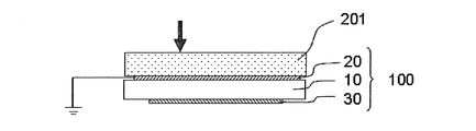
第2実施形態(タッチパネル)、および第3実施形態(電子機器)では、タッチ位置検出用タッチパネル201は、透明圧電シート100のタッチ側とは反対側の面に配置されているが、図5に示すように、変形例1では、これとは逆に、透明圧電シート100のタッチ側の面に配置されている。
タッチ位置検出用タッチパネル201は、透明圧電シート100に直接接触している。
透明圧電シート100の第1透明平板電極20は、透明圧電体膜10のタッチ側の面に配置されたグランド電極であり、タッチ位置検出用タッチパネル201のグランド電極を兼ねている。この構造上の簡略化によって、本変形例のタッチパネル、および電子機器は製造コストが低い。
なお、本変形例のタッチパネル、および電子機器を説明する図5では、タッチ位置検出用タッチパネル201および透明圧電シート100のみを示すが、他の部分は、第2実施形態(タッチパネル)、および第3実施形態(電子機器)と同様である。
図5の矢印に示すタッチの位置は、タッチ位置検出用タッチパネル201によって検出されるとともに、タッチ圧は、透明圧電シート100によって検出される。
図6を参照して、本変形例のタッチパネル、および電子機器を説明する。
図6に示すように、変形例2と同様に、タッチ位置検出用タッチパネル201は、透明圧電シート100のタッチ側の面に配置されている。
透明圧電シート100の第2透明平板電極30は、タッチ側とは反対側の面に配置されてあり、グランド電極である。このように、タッチ側とは反対側にグランド電極が配置されていることにより、本変形例のタッチパネル、および電子機器は、出力電圧のノイズが軽減されている。
図6の矢印に示すタッチの位置は、タッチ位置検出用タッチパネル201によって検出されるとともに、タッチ圧は、透明圧電シート100によって検出される。
図7を参照して、本変形例のタッチパネル、および電子機器を説明する。
図7に示すように、タッチ位置検出用タッチパネル201は、透明圧電シート100のタッチ側とは反対側の面に配置されている。
透明圧電シート100の第2透明平板電極30は、タッチ側とは反対側の面に配置されてあり、グランド電極である。
一方、透明圧電シート100のタッチ側の面には、絶縁層60を介してグランド電極80が配置されている。
図7の矢印に示すタッチの圧力は、透明圧電シート100によって検出されるとともに、タッチ位置は、タッチ位置検出用タッチパネル201によって検出される。
20 第1透明平板電極
20a 第1透明平板電極部
20b 第1リード部
30 第2透明平板電極
30a 第2透明平板電極部
30b 第2リード部
40 フレーム
41 フレーム
42 筐体
42a 開口部
42b 内縁部
43 筐体
43a 開口部
43b 内縁部
50 粘着部
60 絶縁層
70 電線
80 グランド電極
100 透明圧電シート
200 タッチ位置検出用タッチパネル
201 タッチ位置検出用タッチパネル
300 検出回路
301 検出回路
400 表示装置
Claims (19)
- 1個の、有機重合体を含有する透明圧電体膜と、
当該透明圧電体膜の第1主面に配置された1個の第1透明平板電極と、
当該透明圧電体膜の第2主面に配置された1個の第2透明平板電極と、
からなり、
前記第1透明平板電極は、第1透明平板電極部を有し、
前記第2透明平板電極は、第2透明平板電極部を有し、
前記第2透明平板電極部の輪郭が、平面視において前記第1透明平板電極部の輪郭の内側に位置する透明圧電シートと、
前記透明圧電シートの周縁部を覆うフレームと
を含み、
平面視において、前記第1透明平板電極部の輪郭が、前記フレームに完全に重なり、かつ前記第2透明平板電極部の輪郭は、当該フレームに全く重ならない
ことを特徴とするフレーム付透明圧電シート。 - 前記透明圧電体膜の主面の面積に対する前記第2透明平板電極部の面積の比が、70%以上である請求項1に記載のフレーム付透明圧電シート。
- 前記透明圧電体膜の厚さが1~200μmである請求項1または2に記載のフレーム付透明圧電シート。
- 前記有機重合体がフッ化ビニリデン-テトラフルオロエチレン共重合体、フッ化ビニリデン-トリフルオロエチレン共重合体、および、ポリフッ化ビニリデンから選択される有機重合体である、請求項1~3のいずれか1項に記載のフレーム付透明圧電シート。
- 前記第1透明平板電極は、第1リード部を更に有し、かつ
前記第2透明平板電極は、第2リード部を更に有する、
請求項1~4のいずれか1項に記載のフレーム付透明圧電シート。 - 表面上に設けられた粘着部を更に含む請求項1~5のいずれか1項にフレーム付透明圧電シート。
- タッチ圧検出用である請求項1~6のいずれか1項に記載のフレーム付透明圧電シート。
- タッチ位置検出用タッチパネルと組み合わせて用いられる請求項1~7のいずれか1項に記載のフレーム付透明圧電シート。
- 前記タッチ位置検出用タッチパネルが抵抗膜式もしくは静電容量式である請求項8に記載のフレーム付透明圧電シート。
- タッチ位置検出用タッチパネルと、
当該タッチ位置検出用タッチパネルの一方の面上に配置された、請求項1~9のいずれか1項に記載のフレーム付透明圧電シートと
を含むタッチパネル。 - 請求項6に記載のフレーム付透明圧電シートが、前記粘着部によって貼付されている、タッチ位置検出用タッチパネル。
- 請求項6に記載のフレーム付透明圧電シートが、前記粘着部によって貼付されている、ディスプレイ装置。
- 1個の、有機重合体を含有する透明圧電体膜と、
当該透明圧電体膜の第1主面に配置された1個の第1透明平板電極と、
当該透明圧電体膜の第2主面に配置された1個の第2透明平板電極と、
からなり、
前記第1透明平板電極は、第1透明平板電極部を有し、
前記第2透明平板電極は、第2透明平板電極部を有し、
前記第1透明平板電極部の輪郭が、平面視において前記第2透明平板電極部の輪郭の内側に位置する透明圧電シートと、
当該透明圧電シートの一方の面上に配置されたタッチ位置検出用タッチパネルと、
前記透明圧電シートの周縁部および前記タッチ位置検出用タッチパネルの周縁部を覆うフレームと
を含み、
平面視において、前記第1透明平板電極部の輪郭が、前記フレームに完全に重なり、かつ前記第2透明平板電極部の輪郭は、当該フレームに全く重ならない
ことを特徴とするタッチパネル。 - 第1透明平板電極および第2透明平板電極のうちのタッチ側とは反対側の透明平板電極がグランド電極である
請求項13に記載のタッチパネル。 - 前記タッチ側とは反対側の透明平板電極が、前記タッチ位置検出用タッチパネルのグランド電極を兼ねる請求項14に記載のタッチパネル。
- 有機重合体を含有する、1個の透明圧電体膜と、
当該透明圧電体膜の第1主面に配置された1個の第1透明平板電極と、
当該透明圧電体膜の第2主面に配置された1個の第2透明平板電極と、
からなり、
前記第1透明平板電極は、第1透明平板電極部を有し、
前記第2透明平板電極は、第2透明平板電極部を有し、
前記第2透明平板電極部の輪郭が、平面視において前記第1透明平板電極部の輪郭の内側に位置する透明圧電シートと、
当該透明圧電シートを内部に配置する筐体と
を有し、
前記筐体は、開口部を有し、平面視において、前記第1透明平板電極部の輪郭が、前記開口部を画定する内縁部に完全に重なり、かつ前記第2透明平板電極部の輪郭は、当該内縁部に全く重ならない
ことを特徴とする電子装置。 - 前記透明圧電シートのタッチ側とは反対側の面に接して配置されたタッチ位置検出用タッチパネルを更に有する
ことを特徴とする請求項16に記載の電子装置。 - 第1透明平板電極および第2透明平板電極のうちのタッチ側とは反対側の透明平板電極がグランド電極である請求項16または17に記載の電子装置。
- 前記タッチ側とは反対側の透明平板電極が、タッチ位置検出用タッチパネルのグランド電極を兼ねる請求項18に記載の電子装置。
Priority Applications (3)
| Application Number | Priority Date | Filing Date | Title |
|---|---|---|---|
| KR1020127028981A KR101357317B1 (ko) | 2010-04-07 | 2011-02-28 | 투명 압전 시트를 각각 갖는 프레임을 구비한 투명 압전 시트, 터치 패널 및 전자 장치 |
| US13/639,825 US9200970B2 (en) | 2010-04-07 | 2011-02-28 | Transparent piezoelectric sheet-with-A-frame, touch panel, and electronic device each having the transparent piezoelectric sheet |
| CN201180017080.6A CN102822779B (zh) | 2010-04-07 | 2011-02-28 | 分别具有透明压电片的带框架的透明压电片、触摸式面板及电子装置 |
Applications Claiming Priority (2)
| Application Number | Priority Date | Filing Date | Title |
|---|---|---|---|
| JP2010089065A JP5216041B2 (ja) | 2010-04-07 | 2010-04-07 | 透明圧電シートをそれぞれ有するフレーム付透明圧電シート、タッチパネル、および電子装置 |
| JP2010-089065 | 2010-04-07 |
Publications (1)
| Publication Number | Publication Date |
|---|---|
| WO2011125389A1 true WO2011125389A1 (ja) | 2011-10-13 |
Family
ID=44762352
Family Applications (1)
| Application Number | Title | Priority Date | Filing Date |
|---|---|---|---|
| PCT/JP2011/054521 Ceased WO2011125389A1 (ja) | 2010-04-07 | 2011-02-28 | 透明圧電シートをそれぞれ有するフレーム付透明圧電シート、タッチパネル、および電子装置 |
Country Status (6)
| Country | Link |
|---|---|
| US (1) | US9200970B2 (ja) |
| JP (1) | JP5216041B2 (ja) |
| KR (1) | KR101357317B1 (ja) |
| CN (1) | CN102822779B (ja) |
| TW (1) | TWI497360B (ja) |
| WO (1) | WO2011125389A1 (ja) |
Cited By (5)
| Publication number | Priority date | Publication date | Assignee | Title |
|---|---|---|---|---|
| WO2014112494A1 (ja) * | 2013-01-18 | 2014-07-24 | 株式会社村田製作所 | 変位検出センサおよび操作入力装置 |
| WO2014148521A1 (ja) * | 2013-03-21 | 2014-09-25 | 株式会社村田製作所 | 変位センサ、押込量検出センサ、およびタッチ式入力装置 |
| US20140347304A1 (en) * | 2012-02-15 | 2014-11-27 | Murata Manufacturing Co., Ltd. | Touch Type Input Termnal |
| WO2015041130A1 (ja) * | 2013-09-20 | 2015-03-26 | 株式会社村田製作所 | タッチセンサ |
| JP2015155880A (ja) * | 2014-01-14 | 2015-08-27 | 日本写真印刷株式会社 | 圧力センサ |
Families Citing this family (53)
| Publication number | Priority date | Publication date | Assignee | Title |
|---|---|---|---|---|
| JP5442519B2 (ja) * | 2010-04-07 | 2014-03-12 | ダイキン工業株式会社 | 透明圧電シート、それをそれぞれ含有するフレーム付透明圧電シート、タッチ位置検出用タッチパネル、ディスプレイ装置、タッチパネルおよび電子機器 |
| CN103858079B (zh) | 2011-08-11 | 2016-12-14 | 株式会社村田制作所 | 触摸面板 |
| WO2013089048A1 (ja) | 2011-12-16 | 2013-06-20 | 株式会社村田製作所 | タッチ式操作入力装置 |
| WO2013149331A1 (en) | 2012-04-07 | 2013-10-10 | Cambridge Touch Technologies, Ltd. | Pressure sensing display device |
| WO2013165601A1 (en) | 2012-05-03 | 2013-11-07 | Yknots Industries Llc | Moment compensated bending beam sensor for load measurement on platform supported by bending beams |
| US9983715B2 (en) | 2012-12-17 | 2018-05-29 | Apple Inc. | Force detection in touch devices using piezoelectric sensors |
| JP5686443B2 (ja) * | 2013-01-10 | 2015-03-18 | 日本写真印刷株式会社 | 接着層付きフィルム状感圧センサとこれを用いたタッチパッド、タッチ入力機能付き保護パネル及び電子機器 |
| JP6139185B2 (ja) * | 2013-03-07 | 2017-05-31 | 日本写真印刷株式会社 | 圧力検出装置 |
| WO2014149023A1 (en) | 2013-03-15 | 2014-09-25 | Rinand Solutions Llc | Force sensing of inputs through strain analysis |
| JP6084875B2 (ja) * | 2013-03-28 | 2017-02-22 | 京セラ株式会社 | 入力機能付き表示装置、および電子機器 |
| JP6136462B2 (ja) * | 2013-03-29 | 2017-05-31 | 株式会社村田製作所 | 押圧検出センサ、および操作入力装置 |
| JP2015002428A (ja) * | 2013-06-14 | 2015-01-05 | 富士通株式会社 | 携帯端末装置、機能制御方法および機能制御プログラム |
| JP5933845B2 (ja) * | 2013-09-02 | 2016-06-15 | 三井化学株式会社 | 積層体 |
| TW201512916A (zh) * | 2013-09-18 | 2015-04-01 | Wintek Corp | 觸控面板 |
| WO2015041198A1 (ja) * | 2013-09-20 | 2015-03-26 | 株式会社村田製作所 | 押圧検出センサ |
| WO2015053346A1 (ja) * | 2013-10-08 | 2015-04-16 | ダイキン工業株式会社 | 圧電フィルム |
| CN110134283B (zh) * | 2013-10-28 | 2022-10-11 | 苹果公司 | 基于压电的力感测 |
| JP6439250B2 (ja) * | 2013-10-29 | 2018-12-19 | ダイキン工業株式会社 | 積層体 |
| JPWO2015093356A1 (ja) * | 2013-12-17 | 2017-03-16 | 株式会社村田製作所 | 圧電センサの製造方法 |
| AU2015100011B4 (en) | 2014-01-13 | 2015-07-16 | Apple Inc. | Temperature compensating transparent force sensor |
| JP2015184845A (ja) * | 2014-03-24 | 2015-10-22 | 積水化学工業株式会社 | タッチ式入力装置 |
| WO2015156195A1 (ja) * | 2014-04-07 | 2015-10-15 | 株式会社村田製作所 | タッチセンサ |
| WO2016035682A1 (ja) * | 2014-09-03 | 2016-03-10 | 株式会社村田製作所 | タッチ式入力装置、電子機器 |
| KR102480003B1 (ko) | 2014-12-23 | 2022-12-21 | 케임브리지 터치 테크놀로지스 리미티드 | 압력감지 방식 터치 패널 |
| GB2533667B (en) | 2014-12-23 | 2017-07-19 | Cambridge Touch Tech Ltd | Pressure-sensitive touch panel |
| US9612170B2 (en) | 2015-07-21 | 2017-04-04 | Apple Inc. | Transparent strain sensors in an electronic device |
| US10055048B2 (en) | 2015-07-31 | 2018-08-21 | Apple Inc. | Noise adaptive force touch |
| CN107924647A (zh) * | 2015-08-07 | 2018-04-17 | 株式会社村田制作所 | 显示装置 |
| US9874965B2 (en) | 2015-09-11 | 2018-01-23 | Apple Inc. | Transparent strain sensors in an electronic device |
| CN105138182B (zh) * | 2015-09-25 | 2018-11-06 | 京东方科技集团股份有限公司 | 触控显示模组、触控输入单元以及触控输入方法 |
| US9886118B2 (en) | 2015-09-30 | 2018-02-06 | Apple Inc. | Transparent force sensitive structures in an electronic device |
| KR102476610B1 (ko) | 2015-10-02 | 2022-12-12 | 삼성전자주식회사 | 터치 패드, 이를 이용한 터치 스크린 및 전자 장치, 및 터치 패드의 제조 방법 |
| US10635222B2 (en) | 2015-10-02 | 2020-04-28 | Samsung Electronics Co., Ltd. | Touch pad and electronic apparatus using the same, and method of producing touch pad |
| JP6104352B2 (ja) * | 2015-11-18 | 2017-03-29 | 株式会社ディスコ | パシベーション膜が積層されたウエーハのアブレーション加工方法 |
| US10282046B2 (en) | 2015-12-23 | 2019-05-07 | Cambridge Touch Technologies Ltd. | Pressure-sensitive touch panel |
| GB2544353B (en) | 2015-12-23 | 2018-02-21 | Cambridge Touch Tech Ltd | Pressure-sensitive touch panel |
| CN105807988A (zh) * | 2016-02-25 | 2016-07-27 | 京东方科技集团股份有限公司 | 触控显示基板、触控显示屏及触控显示基板的制作方法 |
| US10006820B2 (en) | 2016-03-08 | 2018-06-26 | Apple Inc. | Magnetic interference avoidance in resistive sensors |
| US10209830B2 (en) | 2016-03-31 | 2019-02-19 | Apple Inc. | Electronic device having direction-dependent strain elements |
| JP6690992B2 (ja) * | 2016-05-18 | 2020-04-28 | 株式会社ジャパンディスプレイ | 表示装置 |
| US10133418B2 (en) | 2016-09-07 | 2018-11-20 | Apple Inc. | Force sensing in an electronic device using a single layer of strain-sensitive structures |
| CN109791081B (zh) * | 2016-09-21 | 2022-02-11 | 株式会社村田制作所 | 压电传感器、触摸式输入装置 |
| US10444091B2 (en) | 2017-04-11 | 2019-10-15 | Apple Inc. | Row column architecture for strain sensing |
| CN107205064B (zh) * | 2017-05-23 | 2019-11-15 | 维沃移动通信有限公司 | 一种接地结构及移动终端 |
| US10309846B2 (en) | 2017-07-24 | 2019-06-04 | Apple Inc. | Magnetic field cancellation for strain sensors |
| GB2565305A (en) | 2017-08-08 | 2019-02-13 | Cambridge Touch Tech Ltd | Device for processing signals from a pressure-sensing touch panel |
| US11093088B2 (en) | 2017-08-08 | 2021-08-17 | Cambridge Touch Technologies Ltd. | Device for processing signals from a pressure-sensing touch panel |
| US10782818B2 (en) | 2018-08-29 | 2020-09-22 | Apple Inc. | Load cell array for detection of force input to an electronic device enclosure |
| US10901510B2 (en) | 2018-10-09 | 2021-01-26 | Microsoft Technology Licensing, Llc | Haptic feedback system having two independent actuators |
| CN110286790B (zh) | 2019-06-21 | 2021-11-12 | 京东方科技集团股份有限公司 | 触控面板及显示装置 |
| JP7321112B2 (ja) * | 2020-02-10 | 2023-08-04 | 三菱電機株式会社 | タッチパネルおよびこれを備えた表示装置 |
| CN114981614B (zh) * | 2020-07-30 | 2025-09-16 | 株式会社村田制作所 | 变形检测传感器 |
| TWI761994B (zh) * | 2020-10-16 | 2022-04-21 | 原見精機股份有限公司 | 具備失效偵測機制的接觸感應器 |
Citations (5)
| Publication number | Priority date | Publication date | Assignee | Title |
|---|---|---|---|---|
| JPH0561592A (ja) * | 1991-09-04 | 1993-03-12 | Yamaha Corp | タツチ入力装置 |
| JP2004125571A (ja) * | 2002-10-01 | 2004-04-22 | National Institute Of Advanced Industrial & Technology | 透明圧電センサおよびそれを備えた入力装置 |
| JP2006092428A (ja) * | 2004-09-27 | 2006-04-06 | Nihon Kaiheiki Industry Co Ltd | 感圧式指紋センサ |
| JP2009080090A (ja) * | 2007-09-05 | 2009-04-16 | Erumekku Denshi Kogyo Kk | 圧電センサ |
| JP2010026938A (ja) * | 2008-07-23 | 2010-02-04 | Daikin Ind Ltd | タッチパネル |
Family Cites Families (27)
| Publication number | Priority date | Publication date | Assignee | Title |
|---|---|---|---|---|
| JP3141645B2 (ja) * | 1993-08-23 | 2001-03-05 | 株式会社村田製作所 | 圧力センサ |
| WO2001014842A1 (fr) * | 1999-08-20 | 2001-03-01 | Hitachi, Ltd. | Detecteur de pression semi-conducteur et dispositif de detection de pression |
| JP2004534974A (ja) | 2000-10-27 | 2004-11-18 | エロ・タッチシステムズ・インコーポレイテッド | 複数のタッチセンサを利用した接触確認式タッチスクリーン |
| JP3798287B2 (ja) * | 2001-10-10 | 2006-07-19 | Smk株式会社 | タッチパネル入力装置 |
| WO2004031711A1 (ja) * | 2002-10-01 | 2004-04-15 | National Institute Of Advanced Industrial Science And Technology | 圧電センサおよびそれを備えた入力装置 |
| EP1628350A4 (en) * | 2003-05-22 | 2009-12-02 | Fujitsu Ltd | PIEZOELECTRIC COMPONENT, METHOD FOR ITS MANUFACTURE AND TOUCH PANEL EQUIPMENT |
| US20040263483A1 (en) * | 2003-06-24 | 2004-12-30 | Aufderheide Brian E | Sensing device |
| JP4784041B2 (ja) * | 2003-11-07 | 2011-09-28 | パナソニック株式会社 | タッチパネルを用いた入力装置 |
| WO2005058133A2 (en) * | 2003-12-11 | 2005-06-30 | Proteus Biomedical, Inc. | Implantable pressure sensors |
| JPWO2005064451A1 (ja) * | 2003-12-26 | 2007-12-20 | 日本写真印刷株式会社 | 保護パネル付き電子機器、保護パネル |
| JP4748299B2 (ja) | 2004-12-03 | 2011-08-17 | セイコーエプソン株式会社 | 電子ペーパ及び電子機器 |
| EP1975587A1 (en) * | 2006-01-19 | 2008-10-01 | Fujikura Ltd. | Pressure sensor package and electronic part |
| JPWO2008117770A1 (ja) * | 2007-03-26 | 2010-07-15 | 日本写真印刷株式会社 | 電子機器表示窓のタッチ入力機能付き保護パネル |
| EP2131270A4 (en) * | 2007-03-27 | 2013-04-24 | Kyocera Corp | TOUCH SCREEN AND DISPLAY DEVICE WITH TOUCH SCREEN |
| CN101344447A (zh) * | 2007-07-13 | 2009-01-14 | 清华大学 | 微机电压力传感器 |
| JP2009053109A (ja) * | 2007-08-28 | 2009-03-12 | Aisin Seiki Co Ltd | 圧電フィルムセンサ |
| JP5265163B2 (ja) * | 2007-09-27 | 2013-08-14 | 富士フイルム株式会社 | 圧電デバイスおよび液体吐出ヘッド |
| US8421483B2 (en) * | 2008-06-13 | 2013-04-16 | Sony Ericsson Mobile Communications Ab | Touch and force sensing for input devices |
| US7860668B2 (en) * | 2008-06-18 | 2010-12-28 | Qualcomm Mems Technologies, Inc. | Pressure measurement using a MEMS device |
| JP4664397B2 (ja) * | 2008-06-24 | 2011-04-06 | 日本電波工業株式会社 | 圧電部品及びその製造方法 |
| JP5154316B2 (ja) * | 2008-06-30 | 2013-02-27 | 株式会社ジャパンディスプレイイースト | タッチパネル |
| AT506705B1 (de) * | 2008-09-11 | 2009-11-15 | Piezocryst Advanced Sensorics | Piezoelektrischer drucksensor |
| JP5305028B2 (ja) * | 2008-10-16 | 2013-10-02 | セイコーエプソン株式会社 | 圧力センサー |
| JP5309898B2 (ja) * | 2008-10-31 | 2013-10-09 | セイコーエプソン株式会社 | 圧力センサ装置 |
| US8094134B2 (en) * | 2008-12-25 | 2012-01-10 | Nissha Printing Co., Ltd. | Touch panel having press detection function and pressure sensitive sensor for the touch panel |
| JP5337061B2 (ja) * | 2009-02-20 | 2013-11-06 | セイコーインスツル株式会社 | タッチパネル及びこれを備える表示装置 |
| US8902023B2 (en) * | 2009-06-24 | 2014-12-02 | Avago Technologies General Ip (Singapore) Pte. Ltd. | Acoustic resonator structure having an electrode with a cantilevered portion |
-
2010
- 2010-04-07 JP JP2010089065A patent/JP5216041B2/ja active Active
-
2011
- 2011-02-28 WO PCT/JP2011/054521 patent/WO2011125389A1/ja not_active Ceased
- 2011-02-28 CN CN201180017080.6A patent/CN102822779B/zh not_active Expired - Fee Related
- 2011-02-28 US US13/639,825 patent/US9200970B2/en active Active
- 2011-02-28 KR KR1020127028981A patent/KR101357317B1/ko active Active
- 2011-03-17 TW TW100109174A patent/TWI497360B/zh active
Patent Citations (5)
| Publication number | Priority date | Publication date | Assignee | Title |
|---|---|---|---|---|
| JPH0561592A (ja) * | 1991-09-04 | 1993-03-12 | Yamaha Corp | タツチ入力装置 |
| JP2004125571A (ja) * | 2002-10-01 | 2004-04-22 | National Institute Of Advanced Industrial & Technology | 透明圧電センサおよびそれを備えた入力装置 |
| JP2006092428A (ja) * | 2004-09-27 | 2006-04-06 | Nihon Kaiheiki Industry Co Ltd | 感圧式指紋センサ |
| JP2009080090A (ja) * | 2007-09-05 | 2009-04-16 | Erumekku Denshi Kogyo Kk | 圧電センサ |
| JP2010026938A (ja) * | 2008-07-23 | 2010-02-04 | Daikin Ind Ltd | タッチパネル |
Cited By (11)
| Publication number | Priority date | Publication date | Assignee | Title |
|---|---|---|---|---|
| US20140347304A1 (en) * | 2012-02-15 | 2014-11-27 | Murata Manufacturing Co., Ltd. | Touch Type Input Termnal |
| US9720533B2 (en) * | 2012-02-15 | 2017-08-01 | Murata Manufacturing Co., Ltd. | Touch type input terminal |
| WO2014112494A1 (ja) * | 2013-01-18 | 2014-07-24 | 株式会社村田製作所 | 変位検出センサおよび操作入力装置 |
| JP5804213B2 (ja) * | 2013-01-18 | 2015-11-04 | 株式会社村田製作所 | 変位検出センサおよび操作入力装置 |
| US10101220B2 (en) | 2013-01-18 | 2018-10-16 | Murata Manufacturing Co., Ltd. | Displacement detection sensor and operation input device |
| WO2014148521A1 (ja) * | 2013-03-21 | 2014-09-25 | 株式会社村田製作所 | 変位センサ、押込量検出センサ、およびタッチ式入力装置 |
| WO2015041130A1 (ja) * | 2013-09-20 | 2015-03-26 | 株式会社村田製作所 | タッチセンサ |
| JP5950052B2 (ja) * | 2013-09-20 | 2016-07-13 | 株式会社村田製作所 | タッチセンサ |
| JP2016184425A (ja) * | 2013-09-20 | 2016-10-20 | 株式会社村田製作所 | タッチセンサ |
| US10466827B2 (en) | 2013-09-20 | 2019-11-05 | Murata Manufacturing Co., Ltd. | Touch sensor having piezoelectric detecting electrodes and position detecting electrodes that do not overlap each other |
| JP2015155880A (ja) * | 2014-01-14 | 2015-08-27 | 日本写真印刷株式会社 | 圧力センサ |
Also Published As
| Publication number | Publication date |
|---|---|
| CN102822779A (zh) | 2012-12-12 |
| US9200970B2 (en) | 2015-12-01 |
| CN102822779B (zh) | 2016-06-01 |
| JP2011221721A (ja) | 2011-11-04 |
| KR101357317B1 (ko) | 2014-02-03 |
| TWI497360B (zh) | 2015-08-21 |
| US20130027339A1 (en) | 2013-01-31 |
| KR20130005297A (ko) | 2013-01-15 |
| TW201203044A (en) | 2012-01-16 |
| JP5216041B2 (ja) | 2013-06-19 |
Similar Documents
| Publication | Publication Date | Title |
|---|---|---|
| JP5216041B2 (ja) | 透明圧電シートをそれぞれ有するフレーム付透明圧電シート、タッチパネル、および電子装置 | |
| JP5442519B2 (ja) | 透明圧電シート、それをそれぞれ含有するフレーム付透明圧電シート、タッチ位置検出用タッチパネル、ディスプレイ装置、タッチパネルおよび電子機器 | |
| KR102373330B1 (ko) | 터치 센서를 포함하는 표시 장치 및 그 제조 방법 | |
| JP5689523B1 (ja) | 圧力検出器を備えたタッチパネル | |
| US10503315B2 (en) | Display device | |
| JP5722954B2 (ja) | 押圧検出機能付タッチパネル | |
| KR101626299B1 (ko) | 접착층을 구비한 필름형 감압 센서와 이를 이용한 터치 패드, 터치 입력 기능을 구비한 보호 패널 및 전자 기기 | |
| US9304631B2 (en) | Touch screen panel | |
| US8599321B2 (en) | Touch-sensing display device and touch-sensing module thereof | |
| US11150772B2 (en) | Display device having a non-display area with a sensing portion and a non-sensing portion | |
| KR20150012389A (ko) | 플렉서블 터치 스크린 패널 및 이를 구비한 플렉서블 표시장치 | |
| US20100026648A1 (en) | Touch panel and display unit | |
| US20080018201A1 (en) | Touch panel | |
| CN206532273U (zh) | 触摸传感器以及电子设备 | |
| KR102021218B1 (ko) | 단말 | |
| JP2015084148A (ja) | タッチ式情報入力画像表示装置及び情報機器 | |
| KR20160073278A (ko) | 터치 센서 장치 및 이를 포함하는 표시 장치 | |
| KR20160145423A (ko) | 커버 기판 및 이를 포함하는 터치 디바이스 | |
| TWM416138U (en) | Touch input device |
Legal Events
| Date | Code | Title | Description |
|---|---|---|---|
| WWE | Wipo information: entry into national phase |
Ref document number: 201180017080.6 Country of ref document: CN |
|
| 121 | Ep: the epo has been informed by wipo that ep was designated in this application |
Ref document number: 11765291 Country of ref document: EP Kind code of ref document: A1 |
|
| WWE | Wipo information: entry into national phase |
Ref document number: 13639825 Country of ref document: US |
|
| NENP | Non-entry into the national phase |
Ref country code: DE |
|
| ENP | Entry into the national phase |
Ref document number: 20127028981 Country of ref document: KR Kind code of ref document: A |
|
| 122 | Ep: pct application non-entry in european phase |
Ref document number: 11765291 Country of ref document: EP Kind code of ref document: A1 |