WO2011121932A1 - 光電気化学セル及びそれを用いたエネルギーシステム - Google Patents
光電気化学セル及びそれを用いたエネルギーシステム Download PDFInfo
- Publication number
- WO2011121932A1 WO2011121932A1 PCT/JP2011/001661 JP2011001661W WO2011121932A1 WO 2011121932 A1 WO2011121932 A1 WO 2011121932A1 JP 2011001661 W JP2011001661 W JP 2011001661W WO 2011121932 A1 WO2011121932 A1 WO 2011121932A1
- Authority
- WO
- WIPO (PCT)
- Prior art keywords
- semiconductor layer
- semiconductor
- level
- conductor
- band
- Prior art date
Links
- 239000004065 semiconductor Substances 0.000 claims abstract description 501
- 239000004020 conductor Substances 0.000 claims abstract description 114
- 239000008151 electrolyte solution Substances 0.000 claims abstract description 41
- 239000001257 hydrogen Substances 0.000 claims description 62
- 229910052739 hydrogen Inorganic materials 0.000 claims description 62
- UFHFLCQGNIYNRP-UHFFFAOYSA-N Hydrogen Chemical compound [H][H] UFHFLCQGNIYNRP-UHFFFAOYSA-N 0.000 claims description 60
- 239000000446 fuel Substances 0.000 claims description 13
- 229910052738 indium Inorganic materials 0.000 claims description 11
- APFVFJFRJDLVQX-UHFFFAOYSA-N indium atom Chemical compound [In] APFVFJFRJDLVQX-UHFFFAOYSA-N 0.000 claims description 11
- QCWXUUIWCKQGHC-UHFFFAOYSA-N Zirconium Chemical compound [Zr] QCWXUUIWCKQGHC-UHFFFAOYSA-N 0.000 claims description 10
- 229910052788 barium Inorganic materials 0.000 claims description 10
- DSAJWYNOEDNPEQ-UHFFFAOYSA-N barium atom Chemical compound [Ba] DSAJWYNOEDNPEQ-UHFFFAOYSA-N 0.000 claims description 10
- 229910052726 zirconium Inorganic materials 0.000 claims description 10
- 239000000470 constituent Substances 0.000 claims description 9
- 229910052684 Cerium Inorganic materials 0.000 claims description 5
- 206010021143 Hypoxia Diseases 0.000 claims description 4
- 150000004767 nitrides Chemical class 0.000 claims description 4
- 230000003247 decreasing effect Effects 0.000 claims description 2
- GWXLDORMOJMVQZ-UHFFFAOYSA-N cerium Chemical compound [Ce] GWXLDORMOJMVQZ-UHFFFAOYSA-N 0.000 claims 1
- 239000000463 material Substances 0.000 description 29
- 239000010408 film Substances 0.000 description 27
- 238000006243 chemical reaction Methods 0.000 description 20
- XLYOFNOQVPJJNP-UHFFFAOYSA-N water Substances O XLYOFNOQVPJJNP-UHFFFAOYSA-N 0.000 description 20
- 230000000052 comparative effect Effects 0.000 description 18
- 238000000034 method Methods 0.000 description 17
- 230000004888 barrier function Effects 0.000 description 14
- 230000001443 photoexcitation Effects 0.000 description 14
- 238000003860 storage Methods 0.000 description 14
- 239000000758 substrate Substances 0.000 description 13
- 230000001699 photocatalysis Effects 0.000 description 12
- 239000010409 thin film Substances 0.000 description 12
- GWEVSGVZZGPLCZ-UHFFFAOYSA-N Titan oxide Chemical compound O=[Ti]=O GWEVSGVZZGPLCZ-UHFFFAOYSA-N 0.000 description 11
- OGIDPMRJRNCKJF-UHFFFAOYSA-N titanium oxide Inorganic materials [Ti]=O OGIDPMRJRNCKJF-UHFFFAOYSA-N 0.000 description 11
- QVGXLLKOCUKJST-UHFFFAOYSA-N atomic oxygen Chemical compound [O] QVGXLLKOCUKJST-UHFFFAOYSA-N 0.000 description 9
- 238000010586 diagram Methods 0.000 description 9
- 238000004070 electrodeposition Methods 0.000 description 9
- 239000007789 gas Substances 0.000 description 9
- 239000011521 glass Substances 0.000 description 9
- 239000001301 oxygen Substances 0.000 description 9
- 229910052760 oxygen Inorganic materials 0.000 description 9
- 239000011941 photocatalyst Substances 0.000 description 9
- BASFCYQUMIYNBI-UHFFFAOYSA-N platinum Substances [Pt] BASFCYQUMIYNBI-UHFFFAOYSA-N 0.000 description 7
- 238000005259 measurement Methods 0.000 description 6
- 238000010248 power generation Methods 0.000 description 6
- 239000010936 titanium Substances 0.000 description 6
- 238000004519 manufacturing process Methods 0.000 description 5
- 239000000203 mixture Substances 0.000 description 5
- 238000004544 sputter deposition Methods 0.000 description 5
- 238000005452 bending Methods 0.000 description 4
- ZMIGMASIKSOYAM-UHFFFAOYSA-N cerium Chemical compound [Ce][Ce][Ce][Ce][Ce][Ce][Ce][Ce][Ce][Ce][Ce][Ce][Ce][Ce][Ce][Ce][Ce][Ce][Ce][Ce][Ce][Ce][Ce][Ce][Ce][Ce][Ce][Ce][Ce][Ce][Ce][Ce][Ce][Ce][Ce][Ce][Ce][Ce] ZMIGMASIKSOYAM-UHFFFAOYSA-N 0.000 description 4
- 150000001875 compounds Chemical class 0.000 description 4
- 239000003792 electrolyte Substances 0.000 description 4
- 238000002474 experimental method Methods 0.000 description 4
- 230000001678 irradiating effect Effects 0.000 description 4
- 230000006798 recombination Effects 0.000 description 4
- 238000005215 recombination Methods 0.000 description 4
- 239000007784 solid electrolyte Substances 0.000 description 4
- 238000004402 ultra-violet photoelectron spectroscopy Methods 0.000 description 4
- 230000000694 effects Effects 0.000 description 3
- 229910021645 metal ion Inorganic materials 0.000 description 3
- 238000001420 photoelectron spectroscopy Methods 0.000 description 3
- 238000000926 separation method Methods 0.000 description 3
- 238000000870 ultraviolet spectroscopy Methods 0.000 description 3
- 229910010413 TiO 2 Inorganic materials 0.000 description 2
- 239000000969 carrier Substances 0.000 description 2
- 239000011248 coating agent Substances 0.000 description 2
- 238000000576 coating method Methods 0.000 description 2
- 239000002131 composite material Substances 0.000 description 2
- 230000005611 electricity Effects 0.000 description 2
- -1 hydrogen ions Chemical class 0.000 description 2
- 238000005304 joining Methods 0.000 description 2
- 230000031700 light absorption Effects 0.000 description 2
- 229910052758 niobium Inorganic materials 0.000 description 2
- 229910052697 platinum Inorganic materials 0.000 description 2
- 229920000642 polymer Polymers 0.000 description 2
- 239000000843 powder Substances 0.000 description 2
- 230000002250 progressing effect Effects 0.000 description 2
- 239000011347 resin Substances 0.000 description 2
- 229920005989 resin Polymers 0.000 description 2
- 229910052709 silver Inorganic materials 0.000 description 2
- 239000000243 solution Substances 0.000 description 2
- 239000000126 substance Substances 0.000 description 2
- 229910052719 titanium Inorganic materials 0.000 description 2
- OYPRJOBELJOOCE-UHFFFAOYSA-N Calcium Chemical compound [Ca] OYPRJOBELJOOCE-UHFFFAOYSA-N 0.000 description 1
- RWSOTUBLDIXVET-UHFFFAOYSA-N Dihydrogen sulfide Chemical compound S RWSOTUBLDIXVET-UHFFFAOYSA-N 0.000 description 1
- YCKRFDGAMUMZLT-UHFFFAOYSA-N Fluorine atom Chemical compound [F] YCKRFDGAMUMZLT-UHFFFAOYSA-N 0.000 description 1
- 229910052688 Gadolinium Inorganic materials 0.000 description 1
- GYHNNYVSQQEPJS-UHFFFAOYSA-N Gallium Chemical compound [Ga] GYHNNYVSQQEPJS-UHFFFAOYSA-N 0.000 description 1
- HBBGRARXTFLTSG-UHFFFAOYSA-N Lithium ion Chemical compound [Li+] HBBGRARXTFLTSG-UHFFFAOYSA-N 0.000 description 1
- 229920000557 Nafion® Polymers 0.000 description 1
- RTAQQCXQSZGOHL-UHFFFAOYSA-N Titanium Chemical compound [Ti] RTAQQCXQSZGOHL-UHFFFAOYSA-N 0.000 description 1
- 229910052769 Ytterbium Inorganic materials 0.000 description 1
- 238000010521 absorption reaction Methods 0.000 description 1
- 238000000862 absorption spectrum Methods 0.000 description 1
- 230000002378 acidificating effect Effects 0.000 description 1
- 229910052782 aluminium Inorganic materials 0.000 description 1
- 238000004458 analytical method Methods 0.000 description 1
- 239000007864 aqueous solution Substances 0.000 description 1
- 230000005540 biological transmission Effects 0.000 description 1
- 230000000903 blocking effect Effects 0.000 description 1
- 229910052791 calcium Inorganic materials 0.000 description 1
- 239000011575 calcium Substances 0.000 description 1
- 238000004364 calculation method Methods 0.000 description 1
- 150000004770 chalcogenides Chemical class 0.000 description 1
- 229910052804 chromium Inorganic materials 0.000 description 1
- 238000000354 decomposition reaction Methods 0.000 description 1
- 230000007423 decrease Effects 0.000 description 1
- 238000005868 electrolysis reaction Methods 0.000 description 1
- 229910052731 fluorine Inorganic materials 0.000 description 1
- 239000011737 fluorine Substances 0.000 description 1
- 239000013505 freshwater Substances 0.000 description 1
- UIWYJDYFSGRHKR-UHFFFAOYSA-N gadolinium atom Chemical compound [Gd] UIWYJDYFSGRHKR-UHFFFAOYSA-N 0.000 description 1
- 229910052733 gallium Inorganic materials 0.000 description 1
- 238000004817 gas chromatography Methods 0.000 description 1
- 229910052737 gold Inorganic materials 0.000 description 1
- 229910000037 hydrogen sulfide Inorganic materials 0.000 description 1
- AMGQUBHHOARCQH-UHFFFAOYSA-N indium;oxotin Chemical compound [In].[Sn]=O AMGQUBHHOARCQH-UHFFFAOYSA-N 0.000 description 1
- 239000012212 insulator Substances 0.000 description 1
- 239000003014 ion exchange membrane Substances 0.000 description 1
- 229910001416 lithium ion Inorganic materials 0.000 description 1
- 229910052751 metal Inorganic materials 0.000 description 1
- 239000002184 metal Substances 0.000 description 1
- 229910052759 nickel Inorganic materials 0.000 description 1
- 230000003647 oxidation Effects 0.000 description 1
- 238000007254 oxidation reaction Methods 0.000 description 1
- 239000002245 particle Substances 0.000 description 1
- 239000005518 polymer electrolyte Substances 0.000 description 1
- 238000001028 reflection method Methods 0.000 description 1
- 229910052706 scandium Inorganic materials 0.000 description 1
- SIXSYDAISGFNSX-UHFFFAOYSA-N scandium atom Chemical compound [Sc] SIXSYDAISGFNSX-UHFFFAOYSA-N 0.000 description 1
- 239000007787 solid Substances 0.000 description 1
- 229910052712 strontium Inorganic materials 0.000 description 1
- CIOAGBVUUVVLOB-UHFFFAOYSA-N strontium atom Chemical compound [Sr] CIOAGBVUUVVLOB-UHFFFAOYSA-N 0.000 description 1
- 150000004763 sulfides Chemical class 0.000 description 1
- 229910052715 tantalum Inorganic materials 0.000 description 1
- XOLBLPGZBRYERU-UHFFFAOYSA-N tin dioxide Chemical compound O=[Sn]=O XOLBLPGZBRYERU-UHFFFAOYSA-N 0.000 description 1
- 229910001887 tin oxide Inorganic materials 0.000 description 1
- 229910052720 vanadium Inorganic materials 0.000 description 1
- NAWDYIZEMPQZHO-UHFFFAOYSA-N ytterbium Chemical compound [Yb] NAWDYIZEMPQZHO-UHFFFAOYSA-N 0.000 description 1
- 229910052727 yttrium Inorganic materials 0.000 description 1
- VWQVUPCCIRVNHF-UHFFFAOYSA-N yttrium atom Chemical compound [Y] VWQVUPCCIRVNHF-UHFFFAOYSA-N 0.000 description 1
Images


Classifications
-
- C—CHEMISTRY; METALLURGY
- C25—ELECTROLYTIC OR ELECTROPHORETIC PROCESSES; APPARATUS THEREFOR
- C25B—ELECTROLYTIC OR ELECTROPHORETIC PROCESSES FOR THE PRODUCTION OF COMPOUNDS OR NON-METALS; APPARATUS THEREFOR
- C25B1/00—Electrolytic production of inorganic compounds or non-metals
- C25B1/50—Processes
- C25B1/55—Photoelectrolysis
-
- C—CHEMISTRY; METALLURGY
- C25—ELECTROLYTIC OR ELECTROPHORETIC PROCESSES; APPARATUS THEREFOR
- C25B—ELECTROLYTIC OR ELECTROPHORETIC PROCESSES FOR THE PRODUCTION OF COMPOUNDS OR NON-METALS; APPARATUS THEREFOR
- C25B11/00—Electrodes; Manufacture thereof not otherwise provided for
- C25B11/04—Electrodes; Manufacture thereof not otherwise provided for characterised by the material
- C25B11/051—Electrodes formed of electrocatalysts on a substrate or carrier
- C25B11/073—Electrodes formed of electrocatalysts on a substrate or carrier characterised by the electrocatalyst material
-
- B—PERFORMING OPERATIONS; TRANSPORTING
- B01—PHYSICAL OR CHEMICAL PROCESSES OR APPARATUS IN GENERAL
- B01J—CHEMICAL OR PHYSICAL PROCESSES, e.g. CATALYSIS OR COLLOID CHEMISTRY; THEIR RELEVANT APPARATUS
- B01J35/00—Catalysts, in general, characterised by their form or physical properties
- B01J35/30—Catalysts, in general, characterised by their form or physical properties characterised by their physical properties
- B01J35/39—Photocatalytic properties
-
- H—ELECTRICITY
- H01—ELECTRIC ELEMENTS
- H01M—PROCESSES OR MEANS, e.g. BATTERIES, FOR THE DIRECT CONVERSION OF CHEMICAL ENERGY INTO ELECTRICAL ENERGY
- H01M8/00—Fuel cells; Manufacture thereof
- H01M8/06—Combination of fuel cells with means for production of reactants or for treatment of residues
- H01M8/0606—Combination of fuel cells with means for production of reactants or for treatment of residues with means for production of gaseous reactants
- H01M8/0656—Combination of fuel cells with means for production of reactants or for treatment of residues with means for production of gaseous reactants by electrochemical means
-
- Y—GENERAL TAGGING OF NEW TECHNOLOGICAL DEVELOPMENTS; GENERAL TAGGING OF CROSS-SECTIONAL TECHNOLOGIES SPANNING OVER SEVERAL SECTIONS OF THE IPC; TECHNICAL SUBJECTS COVERED BY FORMER USPC CROSS-REFERENCE ART COLLECTIONS [XRACs] AND DIGESTS
- Y02—TECHNOLOGIES OR APPLICATIONS FOR MITIGATION OR ADAPTATION AGAINST CLIMATE CHANGE
- Y02E—REDUCTION OF GREENHOUSE GAS [GHG] EMISSIONS, RELATED TO ENERGY GENERATION, TRANSMISSION OR DISTRIBUTION
- Y02E60/00—Enabling technologies; Technologies with a potential or indirect contribution to GHG emissions mitigation
- Y02E60/30—Hydrogen technology
- Y02E60/36—Hydrogen production from non-carbon containing sources, e.g. by water electrolysis
-
- Y—GENERAL TAGGING OF NEW TECHNOLOGICAL DEVELOPMENTS; GENERAL TAGGING OF CROSS-SECTIONAL TECHNOLOGIES SPANNING OVER SEVERAL SECTIONS OF THE IPC; TECHNICAL SUBJECTS COVERED BY FORMER USPC CROSS-REFERENCE ART COLLECTIONS [XRACs] AND DIGESTS
- Y02—TECHNOLOGIES OR APPLICATIONS FOR MITIGATION OR ADAPTATION AGAINST CLIMATE CHANGE
- Y02E—REDUCTION OF GREENHOUSE GAS [GHG] EMISSIONS, RELATED TO ENERGY GENERATION, TRANSMISSION OR DISTRIBUTION
- Y02E60/00—Enabling technologies; Technologies with a potential or indirect contribution to GHG emissions mitigation
- Y02E60/30—Hydrogen technology
- Y02E60/50—Fuel cells
-
- Y—GENERAL TAGGING OF NEW TECHNOLOGICAL DEVELOPMENTS; GENERAL TAGGING OF CROSS-SECTIONAL TECHNOLOGIES SPANNING OVER SEVERAL SECTIONS OF THE IPC; TECHNICAL SUBJECTS COVERED BY FORMER USPC CROSS-REFERENCE ART COLLECTIONS [XRACs] AND DIGESTS
- Y02—TECHNOLOGIES OR APPLICATIONS FOR MITIGATION OR ADAPTATION AGAINST CLIMATE CHANGE
- Y02P—CLIMATE CHANGE MITIGATION TECHNOLOGIES IN THE PRODUCTION OR PROCESSING OF GOODS
- Y02P20/00—Technologies relating to chemical industry
- Y02P20/10—Process efficiency
- Y02P20/133—Renewable energy sources, e.g. sunlight
Definitions
- the present invention relates to a photoelectrochemical cell that decomposes water by light irradiation and an energy system using the same.
- Patent Document 1 a technique for decomposing water and collecting hydrogen and oxygen by irradiating a semiconductor material functioning as a photocatalyst with light is known (see, for example, Patent Document 1).
- Patent Document 2 a technique for hydrophilizing the surface of the base material by coating the surface of the base material with the semiconductor material is also known (see, for example, Patent Document 2).
- Patent Document 1 discloses a method of collecting hydrogen and oxygen from the surfaces of both electrodes by disposing an n-type semiconductor electrode and a counter electrode in an electrolyte and irradiating the surfaces of the n-type semiconductor electrode with light. Yes. Specifically, it is described that a TiO 2 electrode, a ZnO electrode, a CdS electrode, or the like can be used as an n-type semiconductor electrode.
- Patent Document 2 discloses a hydrophilic member.
- This hydrophilic member consists of a base material and a film formed on the surface of the base material.
- the coating includes a titanium oxide layer containing titanium oxide particles, and an island-shaped portion made of a second photocatalytic material other than titanium oxide and disposed on the titanium oxide layer.
- Patent Document 2 discloses that the potentials at the lower end of the conduction band and the upper end of the valence band are more positive than titanium oxide with respect to the standard hydrogen electrode potential (the negative side with respect to the vacuum level). ) Is used as the second photocatalytic material.
- This photocatalytic thin film is a film obtained by implanting at least one kind of metal ions such as Nb, V and Cr into a photocatalytic thin film produced on a substrate.
- This film is a tilted film in which the band gap or potential gradient changes in the thickness direction.
- Patent Document 4 a technique for producing hydrogen by irradiating light on a multilayer thin film photocatalyst has been proposed (see Patent Document 4).
- a first compound semiconductor layer and a second compound semiconductor layer having a band gap different from that of the first compound semiconductor layer are sequentially disposed on a conductive substrate. Is formed.
- Hydrogen is produced by immersing the multilayer thin film photocatalyst in a solution containing hydrogen sulfide and irradiating the multilayer thin film photocatalyst with light.
- Patent Document 2 among electrons and holes generated by photoexcitation, electrons move to the conduction band of the second photocatalytic material, and the holes move to the valence band of titanium oxide, so that the electron-hole pair is separated. Therefore, it is described that the probability of recombination of holes and electrons decreases.
- Patent Document 2 does not describe anything about how the energy state at the joint surface between the titanium oxide and the second photocatalytic material is set.
- the junction surface between the titanium oxide and the second photocatalytic material is a Schottky junction
- a Schottky barrier is generated in the conduction band and the valence band at the junction surface.
- Patent Document 2 has a problem that the possibility of recombination of electrons and holes becomes higher than when titanium oxide and the second photocatalyst material are each used alone. It was.
- Patent Document 3 The photocatalytic thin film described in Patent Document 3 is formed into a gradient film by metal ion doping. However, this configuration is obtained for the purpose of improving the light utilization efficiency up to the visible light region by forming the photocatalytic thin film into an inclined film. For this reason, Patent Document 3 describes nothing about how the energy state of the photocatalyst in the inclined film is set. That is, the photocatalytic thin film is not optimized for charge separation or the like.
- the multilayer thin film photocatalyst described in Patent Document 4 has a structure in which two semiconductors CdS and ZnS having different band gaps are joined, and further, this semiconductor ZnS and a conductive substrate Pt are joined.
- Patent Document 4 since such materials having different band gaps are joined, electrons move to the semiconductor ZnS and further to the conductive substrate Pt along the gradient of the band gap, and thus conductive. It is described that it easily binds to hydrogen ions on a conductive substrate and easily generates hydrogen (paragraphs [0026] to [0027] in Patent Document 4).
- the Fermi level (vacuum reference value) of each material is not considered. Therefore, in this configuration, although electrons move along the band gap gradient, it is difficult to move smoothly.
- the present invention can efficiently separate electrons and holes generated by photoexcitation and can improve the quantum efficiency of a hydrogen generation reaction by light irradiation.
- the object is to provide a chemical cell. Furthermore, this invention also aims at providing the energy system using such a photoelectrochemical cell.
- the present invention provides: A semiconductor electrode comprising a conductor and a semiconductor layer disposed on the conductor; A counter electrode electrically connected to the conductor; An electrolyte solution in contact with the surface of the semiconductor layer and the counter electrode; A container for containing the semiconductor electrode, the counter electrode, and the electrolytic solution;
- the vacuum level With reference to the vacuum level, the hand edge level E CS of the conduction band, the band edge level E VS and the Fermi level E FS of the valence band in the region near the surface of the semiconductor layer, and the conductor of the semiconductor layer
- the present invention is further connected to the photoelectrochemical cell of the present invention, the photoelectrochemical cell and a first pipe, and a hydrogen reservoir for storing hydrogen generated in the photoelectrochemical cell;
- an energy system comprising: a fuel cell connected to the hydrogen storage device by a second pipe and converting hydrogen stored in the hydrogen storage device into electric power.
- the photoelectrochemical cell of the present invention can efficiently charge-separate electrons and holes generated by photoexcitation. Thereby, the photoelectrochemical cell of this invention can improve the quantum efficiency of the hydrogen production
- FIG. 1 is a schematic diagram showing the configuration of the photoelectrochemical cell of the present embodiment.
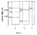
- FIG. 2 is a schematic diagram showing a band structure before bonding of a conductor, a first semiconductor layer, and a second semiconductor layer constituting a semiconductor electrode in the photoelectrochemical cell of the present embodiment.
- FIG. 3 is a schematic diagram showing a band structure after bonding of a conductor constituting the semiconductor electrode, the first semiconductor layer, and the second semiconductor layer in the photoelectrochemical cell of the present embodiment. 2 and 3, the vertical axis indicates the energy level (unit: eV) based on the vacuum level. Note that here, a mode in which an n-type semiconductor is used for the first semiconductor layer and the second semiconductor layer included in the semiconductor electrode will be described.
- the photoelectrochemical cell 100 of the present embodiment includes a semiconductor electrode 120, a counter electrode 130, an electrolytic solution 140, and a container 110.
- the counter electrode 130 is an electrode that makes a pair with the semiconductor electrode 120.
- the electrolytic solution 140 contains water.
- the container 110 accommodates the semiconductor electrode 120, the counter electrode 130, and the electrolyte solution 140, and has an opening.
- the semiconductor electrode 120 and the counter electrode 130 are disposed so that the surfaces thereof are in contact with the electrolytic solution 140.
- a semiconductor layer included in the semiconductor electrode 120 is formed by a first semiconductor layer 122 and a second semiconductor layer 123 which are sequentially arranged over the conductor 121.
- a portion facing the second semiconductor layer 123 of the semiconductor electrode 120 disposed in the container 110 (hereinafter abbreviated as a light incident portion 110 a) is made of a material that transmits light such as sunlight. Has been.
- the conductor 121 in the semiconductor electrode 120 and the counter electrode 130 are electrically connected by a conducting wire 150.
- the counter electrode means an electrode that exchanges electrons with the semiconductor electrode without using an electrolytic solution. Therefore, the counter electrode 130 in this embodiment only needs to be electrically connected to the conductor 121 constituting the semiconductor electrode 120.
- the positional relationship between the counter electrode 130 and the semiconductor electrode 120 is not particularly limited.
- the first semiconductor layer 122 and the second semiconductor layer 123 satisfy the following relationship with reference to the vacuum level.
- E C1 , E V1 , E F1 , E C2 , E V2 , and E F2 are as follows.
- E C1 Band edge level of the conduction band of the first semiconductor layer 122
- E V1 Band edge level of the valence band of the first semiconductor layer 122
- E F1 Fermi level
- E C2 of the first semiconductor layer 122 Band edge level E V2 of the conduction band of the second semiconductor layer 123: Band edge level E F2 of the valence band of the second semiconductor layer 123: Fermi level of the second semiconductor layer 123
- the semiconductor electrode 120 is set to satisfy the following (1) and (2).
- (1) The difference value between the band edge level of the conduction band and the Fermi level in the second semiconductor layer 123 is larger than the difference value in the first semiconductor layer 122.
- (2) The difference value between the Fermi level in the first semiconductor layer 122 and the band edge level of the valence band is larger than the difference value in the second semiconductor layer 123.
- the semiconductor electrode 120 of the present embodiment is set to satisfy the following (I) and (II) with the vacuum level as a reference.
- the difference value between the band edge level of the conduction band in the region near the surface of the semiconductor layer and the Fermi level is larger than the difference value in the region near the junction surface with the conductor of the semiconductor layer.
- the difference value between the Fermi level in the region near the junction surface with the conductor of the semiconductor layer and the band edge level of the valence band is larger than the difference value in the region near the surface of the semiconductor layer.
- the semiconductor electrode 120 of the present embodiment is set so as to satisfy the following (i) to (iv) with reference to the vacuum level.
- the band edge level E CJ of the conduction band in the region near the junction surface with the conductor of the semiconductor layer is higher than ⁇ 4.44 eV.
- the band edge level E VS of the valence band in the region near the surface of the semiconductor layer is lower than ⁇ 5.67 eV.
- the Fermi level E FJ in the region in the vicinity of the junction surface with the conductor of the semiconductor layer satisfies ⁇ 5.67 eV ⁇ E FJ ⁇ 4.44 eV.
- the Fermi level E FS in the region near the surface of the semiconductor layer satisfies ⁇ 5.67 eV ⁇ E FS ⁇ 4.44 eV.
- the Fermi level is higher than the band edge level of the conduction band. Therefore, the difference value between the band edge level of the conduction band and the Fermi level in the conductor 121 (band edge level of the conduction band ⁇ Fermi level) is a negative value. For this reason, the difference value of the conductor 121 is larger than the difference value of the first semiconductor layer 122. Therefore, similarly to the movement of electrons from the second semiconductor layer 123 to the first semiconductor layer 122, the movement of electrons from the first semiconductor layer 122 to the conductor 121 becomes smooth. As a result, the hydrogen generation efficiency is further improved.
- the Fermi level E Fc of the conductor 121 is higher than the band edge level E C1 of the conduction band of the first semiconductor layer 122 and higher than ⁇ 4.44 eV.
- “higher than ⁇ 4.44 eV” at the vacuum level corresponds to “lower than 0 V” at the standard hydrogen electrode potential. Therefore, the Fermi level of the conductor 121 becomes lower than 0 V that is the reduction potential of water. As a result, hydrogen ions are efficiently reduced on the surface of the counter electrode 130 electrically connected to the conductor 121, and hydrogen is efficiently generated.
- the band edge level E V2 of the valence band in the second semiconductor layer 123 in contact with the electrolytic solution 140 is less than ⁇ 5.67 eV.
- “lower than ⁇ 5.67 eV” at the vacuum level corresponds to “higher than 1.23 V” at the standard hydrogen electrode potential. Therefore, the band edge level E V2 of the valence band in the second semiconductor layer 123 becomes higher than 1.23 V that is the oxidation potential of water. As a result, water is efficiently oxidized on the surface of the second semiconductor layer 123, and oxygen is efficiently generated.
- the Fermi levels E F1 and E F2 are based on the vacuum level. Are set so as to satisfy ⁇ 5.67 eV ⁇ E F1 ⁇ 4.44 eV and ⁇ 5.67 eV ⁇ E F2 ⁇ 4.44 eV.
- the conductor 121, the first semiconductor layer 122, and the second semiconductor layer 123 are bonded to each other.
- the hand edge level E C2 of the conduction band of the second semiconductor layer 123, the band edge level E V2 and the Fermi level E F2 of the valence band, and the first semiconductor layer The band edge level E C1 of the conduction band 122, the band edge level E V1 of the valence band, and the Fermi level E F1 are represented by E C2 ⁇ E F2 > E C1 ⁇ E F1 , E F2 ⁇ E V2 ⁇ E F1 -E V1 is satisfied. As a result, no Schottky barrier is generated at the junction surface between the first semiconductor layer 122 and the second semiconductor layer 123.
- the Fermi level E F2 of the second semiconductor layer 123, the Fermi level E F1 of the first semiconductor layer 122, the Fermi level E Fc of the conductor 121 and, The Fermi level E Fs of the electrolytic solution 140 may be set so as to satisfy E Fs ⁇ E Fc ⁇ E F1 ⁇ E F2 . Accordingly, no Schottky barrier is generated on the bonding surfaces of the first semiconductor layer 122, the second semiconductor layer 123, the conductor 121, and the electrolytic solution 140. As a result, higher hydrogen generation efficiency can be realized.
- the carriers move so that the Fermi levels of the conductor 121 and the first semiconductor layer 122 also coincide with each other. As a result, the band edge near the bonding surface of the first semiconductor layer 122 is bent.
- the Fermi level E Fc of the conductor 121 is set to be equal to or higher than the Fermi level E F1 of the first semiconductor layer 122 with the vacuum level as a reference. Therefore, the junction between the conductor 121 and the first semiconductor layer 122 is in ohmic contact.
- the Fermi level E Fc of the conductor 121 is set to be equal to or higher than the Fermi level E F1 of the first semiconductor layer 122 in order to generate hydrogen more efficiently.
- it is not limited to this. Even when the Fermi level E Fc of the conductor 121 is smaller than the Fermi level E F1 of the first semiconductor layer 122, hydrogen can be generated.
- the Fermi level E Fs of the electrolytic solution 140 desirably satisfies the relationship of E Fs ⁇ E Fc ⁇ E F1 ⁇ E F2 . However, even if this relationship is not satisfied, hydrogen can be generated.
- the difference value between the band edge level of the conduction band and the Fermi level in the second semiconductor layer is smaller than the difference value in the first semiconductor layer with reference to the vacuum level.
- the second semiconductor layer is obtained by bending the band edge of the conduction band near the surface of the second semiconductor layer and the difference in the band edge level of the conduction band between the first semiconductor layer and the second semiconductor layer.
- a well-type potential is generated at the band edge level of the conduction band inside. Due to the well-type potential, electrons accumulate in the second semiconductor layer. As a result, the probability of recombination of electrons and holes generated by photoexcitation increases.
- the difference value between the band edge level of the conduction band in the second semiconductor layer 123 and the Fermi level is the difference value in the first semiconductor layer 122. It is set to be larger. Therefore, the well-type potential as described above does not occur at the band edge level of the conduction band inside the second semiconductor layer 123. Therefore, the electrons move to the first semiconductor layer 122 side without accumulating inside the second semiconductor layer 123. As a result, the efficiency of charge separation is greatly improved.
- the difference value between the Fermi level in the first semiconductor layer 122 and the band edge level of the valence band with respect to the vacuum level is the difference in the second semiconductor layer 123.
- a form smaller than the value is assumed.
- a well-type potential is generated at the band edge level of the valence band inside the semiconductor layer. Due to the well-type potential, the holes generated in the second semiconductor layer by photoexcitation are divided and moved in the interface direction with the electrolytic solution and the interface direction with the first semiconductor layer.
- the difference value between the Fermi level in the first semiconductor layer 122 and the band edge level of the valence band is the same as that in the second semiconductor layer 123. It is set to be larger than the difference value. Therefore, the well-type potential as described above does not occur at the band edge level of the valence band inside the second semiconductor layer 223. Therefore, the holes move in the direction of the interface with the electrolytic solution without accumulating in the second semiconductor layer 123. As a result, the efficiency of charge separation is greatly improved.
- the band is bent at the interface between the first semiconductor layer 122 and the second semiconductor layer 123, and no Schottky barrier is generated.
- the electrons move to the conduction band of the first semiconductor layer 122, and the holes move the valence band toward the interface with the electrolyte. Moving. Therefore, electrons and holes are efficiently charge separated without being hindered by the Schottky barrier. Accordingly, the probability that electrons and holes generated inside the second semiconductor layer 123 by photoexcitation are recombined is reduced. As a result, the quantum efficiency of the hydrogen generation reaction by light irradiation is improved.
- the Fermi level of the conductor 121 is set to be larger than the Fermi level of the first semiconductor layer 122.
- the Fermi level, the potential at the bottom of the conduction band (band edge level), and the potential at the top of the valence band (band edge level) of the first semiconductor layer 122 and the second semiconductor layer 123 are a flat band potential and It can be determined using the carrier concentration.
- the flat band potential and carrier concentration of a semiconductor can be obtained from a Mott-Schottky plot measured using a semiconductor to be measured as an electrode.
- these energy levels can also be obtained by measurement using a physical ultraviolet photoelectron spectroscopy (UPS) method or an atmospheric photoelectron spectrometer “AC-3” (manufactured by Riken Keiki Co., Ltd.).
- the potentials (band edge levels) at the top of the valence band of the first semiconductor layer 122 and the second semiconductor layer 123 are the band gap and the first semiconductor layer 122 and the second semiconductor layer obtained by the above method. And the potential at the lower end of the conduction band of 123.
- the band gap of the first semiconductor layer 122 and the second semiconductor layer 123 is obtained from the light absorption edge observed in the light absorption spectrum measurement of the semiconductor to be measured.
- the Fermi level of the conductor 121 can be measured by, for example, photoelectron spectroscopy.
- the n-type semiconductor used for the first semiconductor layer 122 and the second semiconductor layer 123 is one in which the band structure relationship between the first semiconductor layer 122 and the second semiconductor layer 123 satisfies the relationship described above. Just choose. Therefore, the materials of the first semiconductor layer 122 and the second semiconductor layer 123 are not particularly limited.
- the n-type semiconductor used for the first semiconductor layer 122 and the second semiconductor layer 123 is preferably one selected from the group consisting of oxides, nitrides, and oxynitrides.
- the first semiconductor layer 122 and the second semiconductor layer 123 are not dissolved in the electrolytic solution 140 in a state where the semiconductor electrode 120 is in contact with the electrolytic solution 140. Therefore, the photoelectrochemical cell can operate stably.
- the conductor 121 of the semiconductor electrode 120 is in ohmic contact with the first semiconductor layer 122. Therefore, for example, a metal such as Ti, Ni, Ta, Nb, Al, and Ag, or a conductive material such as ITO (Indium Tin Oxide) and FTO (Fluorine doped Tin Oxide) is used as the conductor 121. it can.
- a metal such as Ti, Ni, Ta, Nb, Al, and Ag
- a conductive material such as ITO (Indium Tin Oxide) and FTO (Fluorine doped Tin Oxide) is used as the conductor 121. it can.
- the region of the surface of the conductor 121 that is not covered with the first semiconductor layer 122 is preferably covered with an insulator such as a resin. According to such a configuration, the conductor 121 can be prevented from being dissolved in the electrolytic solution 140.
- the counter electrode 130 It is preferable to use a material with a small overvoltage for the counter electrode 130.
- hydrogen is generated at the counter electrode 130. Therefore, for example, Pt, Au, Ag, or Fe is preferably used as the counter electrode 130.
- the electrolytic solution 140 may be an electrolytic solution containing water.
- the electrolytic solution containing water may be acidic or alkaline.
- pure water as electrolysis water is used as the electrolytic solution 140 that contacts the surface of the second semiconductor layer 123 of the semiconductor electrode 120 and the surface of the counter electrode 130. It is also possible to replace with.
- a Schottky barrier does not occur at the joint surface between the first semiconductor layer 122 and the second semiconductor layer 123. Accordingly, electrons can move from the second semiconductor layer 123 to the first semiconductor layer 122 without being blocked.
- the first semiconductor layer 122 and the second semiconductor layer 123 include barium, strontium, calcium, zirconium, titanium, cerium, gadolinium, gallium, indium, yttrium, ytterbium, and / or scandium. Can be used as oxides, chalcogenides, sulfides, nitrides, oxynitrides, phosphides and the like.
- an oxide containing barium, zirconium, and indium as constituent elements is preferably used.
- the Fermi level E F1 of the first semiconductor layer 122 can be set higher than ⁇ 5.67 eV and lower than ⁇ 4.44 eV with reference to the vacuum level. That is, in terms of the standard hydrogen electrode potential, the Fermi level of the first semiconductor layer 122 can be set higher than 0V and lower than 1.23V.
- the first semiconductor layer 122 may be an oxide of barium, zirconium, and indium, a composite oxide, or a mixture of a composite oxide and an oxide.
- what added metal ions other than an indium to the above compound may be used. Oxides containing barium, zirconium, cerium and indium as constituent elements are also preferably used.
- the p-type semiconductor may be a perovskite-type oxide semiconductor and may include at least one selected from the following general formula A and general formula B.
- Formula A BaZr 1-x M x O 3- ⁇ (Wherein, M is at least one element selected from trivalent elements, x is a numerical value greater than 0 and less than 1 (preferably less than 0.5), and ⁇ is the amount of oxygen deficiency.
- Formula B BaZr x Ce y M 1 -xy O 3- ⁇ (Wherein M is at least one element selected from trivalent elements, x is a numerical value greater than 0 and less than 1, y is a numerical value greater than 0 and less than 1, and x + y ⁇ 1 And ⁇ is the oxygen deficiency and is a numerical value greater than 0 and less than 1.5.)
- an oxide containing barium, zirconium and indium as constituent elements and an oxide containing barium, zirconium, cerium and indium as constituent elements are also preferably used for the second semiconductor layer 123. It is done. Moreover, the material containing at least any one chosen from the said general formula A and general formula B can also be used.
- the carrier concentration of the p-type semiconductor of the second semiconductor layer 123 is preferably lower than the carrier concentration of the p-type semiconductor of the first semiconductor layer 122.
- the p-type semiconductor of the second semiconductor layer 123 is preferably one selected from the group consisting of oxide, nitride, and oxynitride.
- the photoelectrochemical cell can operate stably.
- an oxide containing barium, zirconium, and indium as constituent elements is used for the p-type semiconductor of the first semiconductor layer 123
- barium, zirconium, cerium, and indium are used for the p-type semiconductor of the second semiconductor layer 123.
- examples of a preferable p-type semiconductor for forming a semiconductor layer include BaZr 0.95 In 0.05 O 3- ⁇ , BaZr 0.9 In 0.1 O 3- ⁇ , BaZr 0.875 In 0.125 O 3- ⁇ , BaZr 0.85 In 0.15 O 3- ⁇ , BaZr 0.8 In 0.2 O 3- ⁇ , BaZr 0.75 In 0.25 O 3- ⁇ , BaZr 0.8 Ga 0.2 O 3- ⁇ , BaZr 0.9 Ga 0.1 O 3- ⁇ , BaZr 0.8 Gd 0.2 O 3- ⁇ , BaZr 0.9 Gd 0.1 O 3- ⁇ , BaZr 0.8 Y 0.2 O 3- ⁇ , BaZr 0.4 Ce 0.4 In 0.2 O 3- ⁇ and BaZr 0.6 Ce 0.2 In 0.2 O 3- ⁇ .
- the band edge level (E C ) of the conduction band of these p-type semiconductors the band edge level (E V ) of the valence band, the Fermi level (E F ), and the band edge level of the conduction band.
- Table 1 shows the difference value (E C ⁇ E F ) between the Fermi level and the Fermi level, and the difference value (E F ⁇ E V ) between the band edge level of the valence band and the Fermi level.
- the semiconductor layer provided over the conductor is formed using the first semiconductor layer and the second semiconductor layer (a configuration in which two semiconductor layers are provided over the conductor). Indicated.
- the configuration of the photoelectrochemical cell of the present invention is not limited to this.
- a semiconductor layer provided on a conductor is formed by first to Nth semiconductor layers (N is an integer of 2 or more) arranged in order on the conductor. Also good. Therefore, it is also possible to use a semiconductor electrode in which three or more semiconductor layers are provided on a conductor.
- the N semiconductor layers are provided on the conductor
- two adjacent layers selected from the first to Nth semiconductor layers are connected to the K ⁇ 1th semiconductor layer and the first layer from the conductor side.
- a semiconductor layer of K (K is an integer of 2 to N).
- the (K ⁇ 1) -th semiconductor layer and the K-th semiconductor layer may be set so as to satisfy the following relationship with reference to the vacuum level.
- E C (K-1) Band edge level E V (K-1) of the conduction band of the (K ⁇ 1) th semiconductor layer: Band edge level E F ( K-1) : Fermi level E CK of the K- 1th semiconductor layer: Band edge level E VK of the conduction band of the Kth semiconductor layer E VK : Band edge level E of the valence band of the Kth semiconductor layer FK : Fermi level of the Kth semiconductor layer
- the semiconductor electrode may include a conductor and one semiconductor layer disposed on the conductor.
- the semiconductor layer is composed of two or more elements, and the concentration of at least one element in the semiconductor layer may be increased or decreased along the thickness direction of the semiconductor layer. .
- Such a state of the semiconductor layer can be said to have an inclined composition.
- the region near the surface of the semiconductor layer and the region near the joint surface of the semiconductor layer with the conductor are set so as to satisfy the following relationship with reference to the vacuum level. Good.
- E CJ Band edge level of the conduction band in the region near the junction surface with the conductor of the semiconductor layer
- E VJ Band edge level of the valence band in the region near the junction surface with the conductor of the semiconductor layer
- E FJ Semiconductor layer Fermi level E CV in the region near the junction surface with the conductor: Band edge level E VS of the conduction band in the region near the surface of the semiconductor layer
- E VS Band edge level E FS of the valence band in the region near the surface of the semiconductor layer : Fermi level in the region near the surface of the semiconductor layer
- FIG. 4 is a schematic diagram showing the configuration of the photoelectrochemical cell of the present embodiment.
- the semiconductor electrode 220 includes the conductor 221, the first semiconductor layer 222 disposed on the conductor 221, and the second semiconductor layer 222 disposed on the first semiconductor layer 222.
- a semiconductor layer 223 is provided.
- an insulating layer 224 is disposed on the surface of the conductor 221 opposite to the surface on which the first semiconductor layer 222 is disposed.
- the structures of the conductor 221, the first semiconductor layer 222, and the second semiconductor layer 223 are the same as those of the conductor 121, the first semiconductor layer 122, and the second semiconductor layer 123 in Embodiment 1, respectively.
- the insulating layer 224 is made of, for example, resin or glass.
- the conductor 221 can be prevented from being dissolved in the electrolytic solution 140.
- the structure in which the above-described insulating layer is further provided to the semiconductor electrode including the two semiconductor layers as described in Embodiment 1 is applied.
- Such an insulating layer can also be applied to the semiconductor electrode provided with three or more semiconductor layers and the semiconductor electrode provided with a semiconductor layer having a gradient composition described in the first embodiment.
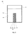
- FIG. 5 is a schematic diagram showing the configuration of the photoelectrochemical cell of the present embodiment.
- the semiconductor electrode 320 includes the conductor 321, the first semiconductor layer 322 disposed on the conductor 321, and the second semiconductor layer 322 disposed on the first semiconductor layer 322.
- a semiconductor layer 323 is provided.
- the counter electrode 330 is disposed on the conductor 321 (on the surface of the conductor 321 opposite to the surface on which the first semiconductor layer 322 is disposed). Note that the structures of the conductor 321, the first semiconductor layer 322, and the second semiconductor layer 323 are the same as those of the conductor 121, the first semiconductor layer 122, and the second semiconductor layer 123 in Embodiment 1, respectively. is there.
- the counter electrode 330 is disposed on the conductor 321 as in the present embodiment, a conductive wire for electrically connecting the semiconductor electrode 320 and the counter electrode 330 becomes unnecessary. As a result, the resistance loss due to the conducting wire is eliminated, so that the quantum efficiency of the hydrogen generation reaction by light irradiation is further improved. Moreover, according to such a structure, the semiconductor electrode 320 and the counter electrode 330 can be electrically connected by a simple process. Note that in this embodiment mode, the structure in which the counter electrode 330 is disposed on the surface of the conductor 321 opposite to the surface on which the first semiconductor layer 322 is disposed is shown.
- the counter electrode 330 is not limited to this configuration, and can be disposed on the same surface as the surface on which the first semiconductor layer 322 is disposed.
- the above-described configuration in which the counter electrode is disposed on the conductor is applied to the photoelectrochemical cell including the two semiconductor layers as described in the first embodiment.
- Such a structure can also be applied to the semiconductor electrode provided with three or more semiconductor layers and the semiconductor electrode provided with a semiconductor layer having a gradient composition, as described in the first embodiment.
- FIG. 6 is a schematic diagram showing the configuration of the photoelectrochemical cell of the present embodiment.
- the photoelectrochemical cell 400 of the present embodiment includes a housing (container) 410, a semiconductor electrode 420, a counter electrode 430, and a separator 460.
- the interior of the housing 410 is separated into two chambers, a first chamber 470 and a second chamber 480, by a separator 460.
- an electrolytic solution 440 containing water is accommodated, respectively.
- a semiconductor electrode 420 is disposed at a position in contact with the electrolytic solution 440.
- the semiconductor electrode 420 includes a conductor 421, a first semiconductor layer 422 disposed on the conductor 421, and a second semiconductor layer 423 disposed on the first semiconductor layer 422.
- the first chamber 470 includes a first exhaust port 471 for exhausting oxygen generated in the first chamber 470 and a water supply port 472 for supplying water into the first chamber 470.
- a portion of the housing 410 facing the second semiconductor layer 423 of the semiconductor electrode 420 disposed in the first chamber 470 (hereinafter referred to as a light incident portion 410a) transmits light such as sunlight. Consists of materials.
- a counter electrode 430 is disposed in the second chamber 480 at a position in contact with the electrolytic solution 440.
- the second chamber 480 includes a second exhaust port 481 for exhausting hydrogen generated in the second chamber 480.
- the conductor 421 and the counter electrode 430 in the semiconductor electrode 420 are electrically connected by a conducting wire 450.
- the conductor 421, the first semiconductor layer 422, and the second semiconductor layer 423 of the semiconductor electrode 420 in this embodiment are the conductor 121, the first semiconductor layer 122, and the second semiconductor layer 120 of the semiconductor electrode 120 in Embodiment 1, respectively.
- Each of the semiconductor layers 123 has the same configuration. Therefore, the semiconductor electrode 420 has the same effects as the semiconductor electrode 120 of the first embodiment.
- the counter electrode 430 and the electrolytic solution 440 are the same as the counter electrode 130 and the electrolytic solution 140 in the first embodiment, respectively.
- the separator 460 is made of a material having a function of allowing the electrolytic solution 440 to pass therethrough and blocking each gas generated in the first chamber 470 and the second chamber 480.
- the material of the separator 460 include a solid electrolyte such as a polymer solid electrolyte.
- the polymer solid electrolyte include an ion exchange membrane such as Nafion (registered trademark).
- the photoelectrochemical cell 400 using the semiconductor electrode 420 having the same configuration as the semiconductor electrode 120 in the first embodiment has been described.
- the semiconductor electrode 420 instead of the semiconductor electrode 420, the semiconductor electrode including the semiconductor layer including three or more semiconductor layers described in Embodiment 1 or the semiconductor layer having a gradient composition is used. It is also possible to use it.
- FIG. 7 is a schematic diagram showing the configuration of the energy system of the present embodiment.
- the energy system 500 of the present embodiment includes a photoelectrochemical cell 400, a hydrogen storage 510, a fuel cell 520, and a storage battery 530.
- the photoelectrochemical cell 400 is the photoelectrochemical cell described in Embodiment 4, and its specific configuration is as shown in FIG. Therefore, detailed description is omitted here.
- the hydrogen storage 510 is connected to the second chamber 480 (see FIG. 6) of the photoelectrochemical cell 400 by the first pipe 541.
- a compressor that compresses hydrogen generated in the photoelectrochemical cell 400 and a high-pressure hydrogen cylinder that stores hydrogen compressed by the compressor can be configured.
- the fuel cell 520 includes a power generation unit 521 and a fuel cell control unit 522 for controlling the power generation unit 521.
- the fuel cell 520 is connected to the hydrogen storage 510 through a second pipe 542.
- the second pipe 542 is provided with a cutoff valve 543.
- a solid polymer electrolyte fuel cell can be used as the fuel cell 520.
- the positive electrode and the negative electrode of the storage battery 530 are electrically connected to the positive electrode and the negative electrode of the power generation unit 521 in the fuel cell 520 by the first wiring 544 and the second wiring 545, respectively.
- the storage battery 530 is provided with a capacity measurement unit 546 for measuring the remaining capacity of the storage battery 530.
- a lithium ion battery can be used as the storage battery 530.
- the second semiconductor layer 423 When sunlight is irradiated on the surface of the second semiconductor layer 423 of the semiconductor electrode 420 disposed in the first chamber 470 through the light incident portion 410a of the photoelectrochemical cell 400, the second semiconductor layer 423 enters the second semiconductor layer 423. Electrons and holes are generated. The holes generated at this time move to the surface side of the second semiconductor layer 423. Thereby, water is decomposed by the reaction formula (1) on the surface of the second semiconductor layer 423 to generate oxygen.
- Oxygen generated in the first chamber 470 is exhausted out of the photoelectrochemical cell 400 through the first exhaust port 471.
- hydrogen generated in the second chamber 480 is supplied into the hydrogen reservoir 510 through the second exhaust port 481 and the first pipe 541.
- the shutoff valve 543 When generating power in the fuel cell 520, the shutoff valve 543 is opened by a signal from the fuel cell control unit 522, and the hydrogen stored in the hydrogen storage 510 is transferred to the power generation unit 521 of the fuel cell 520 by the second pipe 542. Supplied.
- the electricity generated in the power generation unit 521 of the fuel cell 520 is stored in the storage battery 530 via the first wiring 544 and the second wiring 545. Electricity stored in the storage battery 530 is supplied to homes, businesses, and the like by the third wiring 547 and the fourth wiring 548.
- the photoelectrochemical cell 400 it is possible to improve the quantum efficiency of the hydrogen generation reaction by light irradiation. Therefore, according to the energy system 500 of this Embodiment provided with such a photoelectrochemical cell 400, electric power can be supplied efficiently.
- an example of an energy system using the photoelectrochemical cell 400 described in Embodiment 4 is shown.
- the same effect can be obtained in the energy system using the photoelectrochemical cells 100, 200, and 300 described in the first to third embodiments.
- Example 1 As Example 1, a photoelectrochemical cell having the same configuration as the photoelectrochemical cell 200 shown in FIG. 4 was produced. Hereinafter, the photoelectrochemical cell of Example 1 will be described with reference to FIG.
- the photoelectrochemical cell 200 of Example 1 was provided with a square glass container (container 110) having an opening at the top, a semiconductor electrode 220, and a counter electrode.
- a 0.01 mol / L Na 2 SO 3 aqueous solution containing 0.01 mol / L Na 2 S was accommodated as the electrolytic solution 140.
- the semiconductor electrode 220 was produced by the following procedure.
- ITO film (sheet resistance 10 ⁇ / ⁇ ) having a thickness of 150 nm was first formed as a conductor 221 on a 1 cm square glass substrate as the insulating layer 224 by sputtering.
- a BaZr 0.8 In 0.2 O 3- ⁇ film having a thickness of 300 nm was formed as the first semiconductor layer 222 on the conductor 221 by electrodeposition.
- a BaZr 0.9 In 0.1 O 3- ⁇ film having a thickness of 1 ⁇ m was formed as the second semiconductor layer 223 on the first semiconductor layer 222 by the same electrodeposition method.
- the semiconductor electrode 220 was disposed so that the surface of the second semiconductor layer 223 faces the light incident surface 110 a of the glass container 110.
- a platinum plate was used as the counter electrode 130.
- the portion of the conductor 221 of the semiconductor electrode 220 and the counter electrode 130 were electrically connected by the conducting wire 150.
- the current flowing between the semiconductor electrode 220 and the counter electrode 130 was measured with an ammeter.
- Comparative Example 1 In the semiconductor electrode 220 of Example 1, the first semiconductor layer 222 was not provided on the conductor 221 but a BaZr 0.9 In 0.1 O 3- ⁇ film as the second semiconductor layer 223 was provided. Except for this point, the photoelectrochemical cell of Comparative Example 1 was produced by the same procedure as the photoelectrochemical cell 200 of Example 1.
- Comparative Example 2 In the semiconductor electrode 220 of Example 1, a titanium oxide film having a thickness of 1 ⁇ m, which is an n-type semiconductor, was provided instead of the BaZr 0.9 In 0.1 O 3- ⁇ film provided as the second semiconductor layer 223. Except for this point, a photoelectrochemical cell of Comparative Example 2 was produced in the same procedure as in Example 1.
- Comparative Example 3 (Comparative Example 3)
- a Cu 2 O film having a thickness of 1 ⁇ m was provided as the second semiconductor layer 223 instead of the BaZr 0.9 In 0.1 O 3- ⁇ film. Except for this point, a photoelectrochemical cell of Comparative Example 3 was produced in the same procedure as in Example 1.
- Example 2 As Example 2, a photoelectrochemical cell having the same structure as the photoelectrochemical cell 100 shown in FIG. Hereinafter, the photoelectrochemical cell of Example 2 will be described with reference to FIG.
- a Ti substrate was used as the conductor 121.
- a BaZr 0.8 In 0.2 O 3- ⁇ film having a film thickness of 500 nm is formed as the first semiconductor layer 122 by electrodeposition, and a glass substrate as an insulating layer is provided on the back surface of the conductor 121.
- the photoelectrochemical cell 100 of this example is different from the photoelectrochemical cell 200 of Example 1 in that it is insulated by covering the back surface of the conductor 121 with a fluororesin.
- the photoelectrochemical cell 100 of a present Example is the same as that of the photoelectrochemical cell 200 of Example 1, the description is abbreviate
- omitted is abbreviate
- Example 3 As Example 3, a photoelectrochemical cell having the same configuration as the photoelectrochemical cell 300 shown in FIG. 5 was produced. Hereinafter, the photoelectrochemical cell of Example 3 will be described with reference to FIG.
- the semiconductor electrode 320 and the counter electrode 330 were produced by the following procedure.
- a 1 cm square Ti substrate was used.
- a BaZr 0.4 Ce 0.4 In 0.2 O 3- ⁇ film having a thickness of 500 nm was formed as the first semiconductor layer 322 by electrodeposition.
- a 1 ⁇ m-thick BaZr 0.9 In 0.1 O 3- ⁇ film was formed on the first semiconductor layer 322 as the second semiconductor layer 323 by electrodeposition.
- a Pt film having a thickness of 10 nm was formed as a counter electrode 330 on the back surface of the Ti substrate as the conductor 321 by sputtering.
- the semiconductor electrode 320 was disposed so that the surface of the second semiconductor layer 323 faces the light incident surface 110 a of the glass container 110.
- Example 4 As Example 4, a photoelectrochemical cell including a semiconductor electrode in which first to third semiconductor layers were sequentially provided on a conductor was produced. Specifically, the photoelectrochemical cell of Example 4 has a configuration in which a third semiconductor layer is further provided on the second semiconductor layer 223 in the semiconductor electrode 220 of the photoelectrochemical cell 200 shown in FIG. Have Hereinafter, the photoelectrochemical cell of Example 4 will be described with reference to FIG.
- ITO film (sheet resistance 10 ⁇ / ⁇ ) having a thickness of 150 nm was first formed as a conductor 221 on a 1 cm square glass substrate as the insulating layer 224 by sputtering.
- a BaZr 0.8 In 0.2 O 3- ⁇ film having a thickness of 300 nm was formed as the first semiconductor layer 222 on the conductor 221 by electrodeposition.
- a BaZr 0.9 In 0.1 O 3- ⁇ film having a thickness of 500 nm was formed as the second semiconductor layer 223 on the first semiconductor layer 222 by the same electrodeposition method.
- a BaZr 0.95 In 0.05 O 3- ⁇ film with a thickness of 1 ⁇ m was formed as a third semiconductor layer on the second semiconductor layer 223 by the same electrodeposition method.
- the semiconductor electrode 220 was disposed such that the surface of the third semiconductor layer was opposed to the light incident surface 110 a of the glass container 110.
- the optoelectricity of the fifth embodiment is similar to that of the first embodiment except that the materials of the first semiconductor layer 222 and the second semiconductor layer 223 are replaced with n-type semiconductors.
- a chemical cell was made.
- As the first semiconductor layer 222 a 300 nm-thick TiO 2 film was formed by electrodeposition.
- the band edge level of the conduction band of titanium oxide was ⁇ 4.24 eV
- the band edge level of the valence band was ⁇ 7.44 eV
- the Fermi level was ⁇ 4.84 eV
- the band edge level of the conduction band of CdS was ⁇ 4.04 eV
- the band edge level of the valence band was ⁇ 6.54 eV
- the Fermi level was ⁇ 5.24 eV.
- the Fermi level, the band edge level of the conduction band, and the band edge level of the valence band are values based on the vacuum level.
- the vacuum level ⁇ 4.44 eV corresponds to the standard hydrogen electrode potential of 0V.
- the pH value of the electrolyte actually used is about 7
- the Fermi level of the semiconductor is dragged to the Fermi level of the electrolyte having a pH value of 7 and a temperature of 25 ° C.
- the pH value is 7 Therefore, it is considered that the temperature is lowered to the same level as the Fermi level of the electrolyte solution at a temperature of 25 ° C.
- the semiconductor electrode in each photoelectrochemical cell according to Examples 1 to 3 has the band edge level of the conduction band and the band edge level of the valence band of the second semiconductor layer, respectively. It was larger than the band edge level of the conduction band of the first semiconductor layer and the band edge level of the valence band. Moreover, both Fermi levels were the same. Therefore, the value obtained by subtracting the Fermi level from the band edge level of the conduction band of the second semiconductor layer was larger than that of the first semiconductor layer. Further, the value obtained by subtracting the band edge level of the conduction band from the Fermi level of the second semiconductor layer was smaller than that of the first semiconductor layer.
- the Fermi level of the semiconductors used in Examples 1 to 3 was ⁇ 5.08 eV, which was within the range of ⁇ 5.67 eV to ⁇ 4.44 eV.
- the band edge level of the conduction band of the first semiconductor layer was higher than ⁇ 4.44 eV.
- the band edge level of the valence band of the second semiconductor layer was lower than ⁇ 5.67 eV. Therefore, the photoelectrochemical cells of Examples 1 to 3 satisfied the configuration of the semiconductor electrode in the present invention.
- the semiconductor electrodes in the photoelectrochemical cell of Example 4 were provided with first to third semiconductor layers.
- the band structure relationship between two semiconductor layers adjacent to each other is the same between the semiconductor layers described in the first embodiment.
- n-type semiconductors were used for the first semiconductor layer and the second semiconductor layer.
- the band edge level of the conduction band and the band edge level of the valence band of the second semiconductor layer are respectively higher than the band edge level of the conduction band and the band edge level of the valence band of the first semiconductor layer. It was big. Further, the Fermi level was larger in the first semiconductor layer than in the second semiconductor layer. Therefore, the value obtained by subtracting the Fermi level from the band edge level of the conduction band of the second semiconductor layer was larger than that of the first semiconductor layer. Further, the value obtained by subtracting the band edge level of the conduction band from the Fermi level of the second semiconductor layer was smaller than that of the first semiconductor layer.
- the Fermi level of the first semiconductor layer used in Example 5 is ⁇ 4.84 eV
- the Fermi level of the second semiconductor layer is ⁇ 5.24 eV, which is within the range of ⁇ 5.67 eV to ⁇ 4.44 eV. Met.
- the band edge level of the conduction band of the first semiconductor layer was higher than ⁇ 4.44 eV
- the band edge level of the valence band of the second semiconductor layer was lower than ⁇ 5.67 eV. Therefore, the photoelectrochemical cell of Example 5 satisfied the configuration of the semiconductor electrode in the present invention.
- the photoelectrochemical cell of Comparative Example 3 did not satisfy the requirements of the photoelectrochemical cell of the present invention.
- Apparent quantum efficiency ⁇ (observed photocurrent density [mA / cm 2 ]) / (photocurrent density that can be generated by sunlight that can be absorbed in the band gap of the semiconductor material used for the second semiconductor layer [mA / Cm 2 ]) ⁇ ⁇ 100
- the photoelectrochemical cell of Comparative Example 2 was irradiated with light. Although gas generation was observed on the surface of the counter electrode, it was not possible to detect it due to the small amount of gas generated.
- the Fermi level of the first semiconductor layer (p-type semiconductor layer) on the conductor side is the second semiconductor layer ( It was smaller than the Fermi level of the n-type semiconductor layer.
- a Schottky barrier is generated at the junction surface between the first semiconductor layer and the second semiconductor layer. For this reason, electrons and holes generated in the second semiconductor layer by photoexcitation are not separated by charge, and the probability that the generated electrons and holes are recombined increases, and hydrogen cannot be generated efficiently. Conceivable.
- Example 5 the apparent quantum efficiency of CdS alone was about 5%, but the apparent quantum efficiency of the photoelectrochemical cell in Example 5 was 15%. From this result, according to the semiconductor electrode comprising a plurality of semiconductor layers and the relationship of the band structure between the plurality of semiconductor layers satisfying the requirements of the present invention, hydrogen can be generated more efficiently than using each semiconductor material alone. It was confirmed that
- the apparent quantum efficiency was also measured for photoelectrochemical cells in which the materials of the p-type semiconductor shown in Table 1 were used in various combinations to satisfy the configuration of the semiconductor electrode in the present invention. As a result, the apparent quantum efficiency was 40% at the maximum.
- BaZr 0.8 In 0.2 O 3- ⁇ is used for the first semiconductor layer
- BaZr 0.8 In 0.2 O 3- is used for the first semiconductor layer
- BaZr 0.4 Ce 0.4 In 0.2 O 3- ⁇ may be used instead.
- the BaZr 0.4 Ce 0.4 In 0.2 O 3- ⁇ film can be formed, for example, by sputtering.
- the band edge level of the conduction band and the band edge level of the valence band are as shown in Table 1.
- the semiconductor electrode using these also satisfies the requirements for the semiconductor electrode in the present invention. From this, it is estimated that the apparent quantum efficiency is improved as in the case of the first embodiment.
- the band edge level of the conduction band, the band edge level of the valence band, and the band gap shown in Table 1 are measured by UPS, AC-3, or UV-Vis spectroscopy (UV-Vis). It is an actually measured value.
- UPS a sample obtained by electrodepositing a powder sample on a Pt substrate was used for photoelectron spectroscopy measurement in vacuum.
- AC-3 atmospheric photoelectron spectroscopy measurement was performed with an atmospheric photoelectron spectrometer “AC-3” (manufactured by Riken Keiki Co., Ltd.) using a bulk disk sample (diameter 12 cm ⁇ thickness 0.5 cm).
- UV-Vis absorption spectroscopic measurement was performed on a bulk disk sample or a powder sample by the transmission method or the diffuse reflection method.
- the quantum efficiency of the hydrogen generation reaction by light irradiation can be improved, so that it is useful as a household power generation system.
Landscapes
- Chemical & Material Sciences (AREA)
- Engineering & Computer Science (AREA)
- Chemical Kinetics & Catalysis (AREA)
- Electrochemistry (AREA)
- Materials Engineering (AREA)
- Metallurgy (AREA)
- Organic Chemistry (AREA)
- Inorganic Chemistry (AREA)
- Electrolytic Production Of Non-Metals, Compounds, Apparatuses Therefor (AREA)
- Electrodes For Compound Or Non-Metal Manufacture (AREA)
- Inorganic Compounds Of Heavy Metals (AREA)
- Hybrid Cells (AREA)
Priority Applications (4)
| Application Number | Priority Date | Filing Date | Title |
|---|---|---|---|
| JP2012508059A JP5678035B2 (ja) | 2010-03-31 | 2011-03-22 | 光電気化学セル及びそれを用いたエネルギーシステム |
| EP11762184.7A EP2555314B1 (de) | 2010-03-31 | 2011-03-22 | Photoelektrochemische zelle und energiesystem damit |
| CN201180003543.3A CN102484303B (zh) | 2010-03-31 | 2011-03-22 | 光电化学元件和使用该元件的能量系统 |
| US13/393,107 US9157155B2 (en) | 2010-03-31 | 2011-03-22 | Photoelectrochemical cell and energy system using same |
Applications Claiming Priority (2)
| Application Number | Priority Date | Filing Date | Title |
|---|---|---|---|
| JP2010-083418 | 2010-03-31 | ||
| JP2010083418 | 2010-03-31 |
Publications (1)
| Publication Number | Publication Date |
|---|---|
| WO2011121932A1 true WO2011121932A1 (ja) | 2011-10-06 |
Family
ID=44711700
Family Applications (1)
| Application Number | Title | Priority Date | Filing Date |
|---|---|---|---|
| PCT/JP2011/001661 WO2011121932A1 (ja) | 2010-03-31 | 2011-03-22 | 光電気化学セル及びそれを用いたエネルギーシステム |
Country Status (5)
| Country | Link |
|---|---|
| US (1) | US9157155B2 (de) |
| EP (1) | EP2555314B1 (de) |
| JP (1) | JP5678035B2 (de) |
| CN (1) | CN102484303B (de) |
| WO (1) | WO2011121932A1 (de) |
Cited By (8)
| Publication number | Priority date | Publication date | Assignee | Title |
|---|---|---|---|---|
| JP2013209735A (ja) * | 2012-03-30 | 2013-10-10 | Equos Research Co Ltd | 太陽光利用システム |
| WO2014068944A1 (ja) * | 2012-10-31 | 2014-05-08 | パナソニック株式会社 | 光半導体電極、光電気化学セル及びエネルギーシステム |
| WO2014174824A1 (ja) * | 2013-04-26 | 2014-10-30 | パナソニック株式会社 | 光半導体電極、およびそれを具備する光電気化学セル用いて水を光分解する方法 |
| JP5678035B2 (ja) * | 2010-03-31 | 2015-02-25 | パナソニックIpマネジメント株式会社 | 光電気化学セル及びそれを用いたエネルギーシステム |
| JP2015180765A (ja) * | 2014-03-04 | 2015-10-15 | 株式会社デンソー | 二酸化炭素還元電極及びこれを用いた二酸化炭素還元装置 |
| JP2016034611A (ja) * | 2014-08-01 | 2016-03-17 | 株式会社デンソー | 半導体光触媒およびそれを適用した人工光合成装置 |
| JP2019011488A (ja) * | 2017-06-29 | 2019-01-24 | 富士通株式会社 | 酸素発生電極及び酸素発生装置 |
| JP2020091949A (ja) * | 2018-12-03 | 2020-06-11 | 国立大学法人 東京大学 | 混合伝導体層を有する固体酸化物燃料電池 |
Families Citing this family (9)
| Publication number | Priority date | Publication date | Assignee | Title |
|---|---|---|---|---|
| US8147599B2 (en) | 2009-02-17 | 2012-04-03 | Mcalister Technologies, Llc | Apparatuses and methods for storing and/or filtering a substance |
| WO2013025654A2 (en) | 2011-08-12 | 2013-02-21 | Mcalister Technologies, Llc | Fluid distribution filter having spiral filter media and associated systems and methods |
| TWI500211B (zh) * | 2012-12-14 | 2015-09-11 | Hwang Bing Joe | 媒子型光電池系統 |
| US20140272640A1 (en) * | 2013-03-15 | 2014-09-18 | Mcalister Technologies, Llc | Multifunctional electrochemical devices |
| WO2014145882A1 (en) | 2013-03-15 | 2014-09-18 | Mcalister Technologies, Llc | Methods of manufacture of engineered materials and devices |
| WO2014194124A1 (en) | 2013-05-29 | 2014-12-04 | Mcalister Technologies, Llc | Methods for fuel tank recycling and net hydrogen fuel and carbon goods production along with associated apparatus and systems |
| JP2015227503A (ja) * | 2014-05-09 | 2015-12-17 | パナソニックIpマネジメント株式会社 | 水を分解することによって水素を発生させる方法、ならびにそのために用いられる光電気化学セルおよび半導体電極 |
| US9790602B2 (en) * | 2014-08-11 | 2017-10-17 | International Business Machines Corporation | Techniques for photocatalytic hydrogen generation |
| US11473193B2 (en) * | 2019-04-30 | 2022-10-18 | King Fahd University Of Petroleum And Minerals | Fabrication, characterization and photoelectrochemical properties of CeO2-TiO2 thin film electrodes |
Citations (9)
| Publication number | Priority date | Publication date | Assignee | Title |
|---|---|---|---|---|
| JPS51123779A (en) | 1975-04-23 | 1976-10-28 | Kenichi Honda | A hydrogen-oxygen drawing method using electrochemical photoelectric c ells |
| JP2002143688A (ja) | 2000-11-07 | 2002-05-21 | Japan Atom Energy Res Inst | 高効率光触媒薄膜及びその製造方法 |
| JP2002234105A (ja) | 2000-03-13 | 2002-08-20 | Toto Ltd | 親水性部材及びその製造方法 |
| JP2003154272A (ja) | 2001-11-21 | 2003-05-27 | Japan Science & Technology Corp | 多層薄膜状光触媒の作製方法、およびその多層薄膜状光触媒を用いた水素の製造方法 |
| JP2009507752A (ja) * | 2005-09-09 | 2009-02-26 | ユニバーシティ・オブ・ネバダ・リノ | 酸素空孔を有するナノチューブ状チタニア基材の製造及び水の光電気分解におけるそれらの使用 |
| JP2009519204A (ja) * | 2005-12-13 | 2009-05-14 | ユニバーシティ・オブ・ネバダ・リノ | デポジットした金及び炭素粒子を有するナノチューブチタニア基材の製造及び水の光電気分解でのそれらの使用 |
| JP2009527879A (ja) * | 2006-02-22 | 2009-07-30 | ソニー ドイチュラント ゲゼルシャフト ミット ベシュレンクテル ハフツング | 光活性デバイスに利用される半導体材料の伝導帯と価電子帯のバンドエッジポジションを最適化する方法 |
| WO2010050226A1 (ja) * | 2008-10-30 | 2010-05-06 | パナソニック株式会社 | 光電気化学セル及びそれを用いたエネルギーシステム |
| WO2011016244A1 (ja) * | 2009-08-05 | 2011-02-10 | パナソニック株式会社 | 光電気化学セル及びそれを用いたエネルギーシステム |
Family Cites Families (7)
| Publication number | Priority date | Publication date | Assignee | Title |
|---|---|---|---|---|
| US4021323A (en) * | 1975-07-28 | 1977-05-03 | Texas Instruments Incorporated | Solar energy conversion |
| US4181593A (en) | 1978-06-22 | 1980-01-01 | Gte Laboratories Incorporated | Modified titanium dioxide photoactive electrodes |
| US4439301A (en) * | 1982-10-07 | 1984-03-27 | The United States Of America As Represented By The Administrator Of The National Aeronautics And Space Administration | Photoelectrochemical cells including chalcogenophosphate photoelectrodes |
| US4466869A (en) * | 1983-08-15 | 1984-08-21 | Energy Conversion Devices, Inc. | Photolytic production of hydrogen |
| CN100559615C (zh) * | 2008-05-21 | 2009-11-11 | 北京化工大学 | 一种基于无机纳米片的光电转换薄膜及其制备方法 |
| WO2010125787A1 (ja) * | 2009-04-28 | 2010-11-04 | パナソニック株式会社 | 光励起半導体及びそれを用いたデバイス |
| US9157155B2 (en) * | 2010-03-31 | 2015-10-13 | Panasonic Intellectual Property Management Co., Ltd. | Photoelectrochemical cell and energy system using same |
-
2011
- 2011-03-22 US US13/393,107 patent/US9157155B2/en not_active Expired - Fee Related
- 2011-03-22 EP EP11762184.7A patent/EP2555314B1/de not_active Not-in-force
- 2011-03-22 JP JP2012508059A patent/JP5678035B2/ja not_active Expired - Fee Related
- 2011-03-22 CN CN201180003543.3A patent/CN102484303B/zh not_active Expired - Fee Related
- 2011-03-22 WO PCT/JP2011/001661 patent/WO2011121932A1/ja active Application Filing
Patent Citations (9)
| Publication number | Priority date | Publication date | Assignee | Title |
|---|---|---|---|---|
| JPS51123779A (en) | 1975-04-23 | 1976-10-28 | Kenichi Honda | A hydrogen-oxygen drawing method using electrochemical photoelectric c ells |
| JP2002234105A (ja) | 2000-03-13 | 2002-08-20 | Toto Ltd | 親水性部材及びその製造方法 |
| JP2002143688A (ja) | 2000-11-07 | 2002-05-21 | Japan Atom Energy Res Inst | 高効率光触媒薄膜及びその製造方法 |
| JP2003154272A (ja) | 2001-11-21 | 2003-05-27 | Japan Science & Technology Corp | 多層薄膜状光触媒の作製方法、およびその多層薄膜状光触媒を用いた水素の製造方法 |
| JP2009507752A (ja) * | 2005-09-09 | 2009-02-26 | ユニバーシティ・オブ・ネバダ・リノ | 酸素空孔を有するナノチューブ状チタニア基材の製造及び水の光電気分解におけるそれらの使用 |
| JP2009519204A (ja) * | 2005-12-13 | 2009-05-14 | ユニバーシティ・オブ・ネバダ・リノ | デポジットした金及び炭素粒子を有するナノチューブチタニア基材の製造及び水の光電気分解でのそれらの使用 |
| JP2009527879A (ja) * | 2006-02-22 | 2009-07-30 | ソニー ドイチュラント ゲゼルシャフト ミット ベシュレンクテル ハフツング | 光活性デバイスに利用される半導体材料の伝導帯と価電子帯のバンドエッジポジションを最適化する方法 |
| WO2010050226A1 (ja) * | 2008-10-30 | 2010-05-06 | パナソニック株式会社 | 光電気化学セル及びそれを用いたエネルギーシステム |
| WO2011016244A1 (ja) * | 2009-08-05 | 2011-02-10 | パナソニック株式会社 | 光電気化学セル及びそれを用いたエネルギーシステム |
Non-Patent Citations (1)
| Title |
|---|
| See also references of EP2555314A4 |
Cited By (13)
| Publication number | Priority date | Publication date | Assignee | Title |
|---|---|---|---|---|
| JP5678035B2 (ja) * | 2010-03-31 | 2015-02-25 | パナソニックIpマネジメント株式会社 | 光電気化学セル及びそれを用いたエネルギーシステム |
| JP2013209735A (ja) * | 2012-03-30 | 2013-10-10 | Equos Research Co Ltd | 太陽光利用システム |
| WO2014068944A1 (ja) * | 2012-10-31 | 2014-05-08 | パナソニック株式会社 | 光半導体電極、光電気化学セル及びエネルギーシステム |
| JP5677626B2 (ja) * | 2012-10-31 | 2015-02-25 | パナソニックIpマネジメント株式会社 | 光半導体電極、光電気化学セル及びエネルギーシステム |
| JPWO2014174824A1 (ja) * | 2013-04-26 | 2017-02-23 | パナソニック株式会社 | 光半導体電極、およびそれを具備する光電気化学セルを用いて水を光分解する方法 |
| WO2014174824A1 (ja) * | 2013-04-26 | 2014-10-30 | パナソニック株式会社 | 光半導体電極、およびそれを具備する光電気化学セル用いて水を光分解する方法 |
| JP2015180765A (ja) * | 2014-03-04 | 2015-10-15 | 株式会社デンソー | 二酸化炭素還元電極及びこれを用いた二酸化炭素還元装置 |
| JP2016034611A (ja) * | 2014-08-01 | 2016-03-17 | 株式会社デンソー | 半導体光触媒およびそれを適用した人工光合成装置 |
| US9951429B2 (en) | 2014-08-01 | 2018-04-24 | Denso Corporation | Semiconductor photocatalyst and artificial photonic synthesis device having the same |
| JP2019011488A (ja) * | 2017-06-29 | 2019-01-24 | 富士通株式会社 | 酸素発生電極及び酸素発生装置 |
| US11087930B2 (en) | 2017-06-29 | 2021-08-10 | Fujitsu Limited | Oxygen generation apparatus |
| JP2020091949A (ja) * | 2018-12-03 | 2020-06-11 | 国立大学法人 東京大学 | 混合伝導体層を有する固体酸化物燃料電池 |
| JP7194936B2 (ja) | 2018-12-03 | 2022-12-23 | 国立大学法人 東京大学 | 混合伝導体層を有する固体酸化物燃料電池 |
Also Published As
| Publication number | Publication date |
|---|---|
| EP2555314A1 (de) | 2013-02-06 |
| CN102484303A (zh) | 2012-05-30 |
| EP2555314B1 (de) | 2016-09-21 |
| US20120156578A1 (en) | 2012-06-21 |
| EP2555314A4 (de) | 2014-10-08 |
| JP5678035B2 (ja) | 2015-02-25 |
| JPWO2011121932A1 (ja) | 2013-07-04 |
| CN102484303B (zh) | 2015-12-09 |
| US9157155B2 (en) | 2015-10-13 |
Similar Documents
| Publication | Publication Date | Title |
|---|---|---|
| JP5678035B2 (ja) | 光電気化学セル及びそれを用いたエネルギーシステム | |
| JP4494528B1 (ja) | 光電気化学セル及びそれを用いたエネルギーシステム | |
| JP4791614B2 (ja) | 光電気化学セル及びそれを用いたエネルギーシステム | |
| JP5274663B2 (ja) | 光電気化学セル及びそれを用いたエネルギーシステム | |
| KR102014990B1 (ko) | 광전극 구조체용 복합 보호층, 이를 포함하는 광전극 구조체 및 이를 포함하는 광전기화학 전지 | |
| JP5830527B2 (ja) | 半導体素子、水素製造システム、並びにメタンまたはメタノール製造システム | |
| Li et al. | Highly efficient NiFe nanoparticle decorated Si photoanode for photoelectrochemical water oxidation | |
| JP5677626B2 (ja) | 光半導体電極、光電気化学セル及びエネルギーシステム | |
| CN104577166A (zh) | 光半导体电极、光电化学电池、氢产生方法和能量系统 | |
| Chen et al. | Stable CdTe photoanodes with energetics matching those of a coating intermediate band | |
| JP4980497B2 (ja) | 光半導体、それを用いた光半導体電極及び光電気化学セル、並びに、エネルギーシステム | |
| JP2015098643A (ja) | 光電気化学セル及びそれを用いた水素発生方法 | |
| JP2012114017A (ja) | 光電気化学電池及びそれを用いたエネルギーシステム | |
| JP2012114016A (ja) | 光電気化学電池及びそれを用いたエネルギーシステム | |
| Wu et al. | Electrolyte‐Free Fuel Cell: Principles and Crosslink Research |
Legal Events
| Date | Code | Title | Description |
|---|---|---|---|
| WWE | Wipo information: entry into national phase |
Ref document number: 201180003543.3 Country of ref document: CN |
|
| 121 | Ep: the epo has been informed by wipo that ep was designated in this application |
Ref document number: 11762184 Country of ref document: EP Kind code of ref document: A1 |
|
| WWE | Wipo information: entry into national phase |
Ref document number: 2012508059 Country of ref document: JP |
|
| REEP | Request for entry into the european phase |
Ref document number: 2011762184 Country of ref document: EP |
|
| WWE | Wipo information: entry into national phase |
Ref document number: 2011762184 Country of ref document: EP |
|
| WWE | Wipo information: entry into national phase |
Ref document number: 13393107 Country of ref document: US Ref document number: 493/MUMNP/2012 Country of ref document: IN |
|
| NENP | Non-entry into the national phase |
Ref country code: DE |