WO2011108705A1 - 感光性樹脂組成物 - Google Patents
感光性樹脂組成物 Download PDFInfo
- Publication number
- WO2011108705A1 WO2011108705A1 PCT/JP2011/055074 JP2011055074W WO2011108705A1 WO 2011108705 A1 WO2011108705 A1 WO 2011108705A1 JP 2011055074 W JP2011055074 W JP 2011055074W WO 2011108705 A1 WO2011108705 A1 WO 2011108705A1
- Authority
- WO
- WIPO (PCT)
- Prior art keywords
- group
- resin composition
- photosensitive resin
- carbon atoms
- general formula
- Prior art date
- Legal status (The legal status is an assumption and is not a legal conclusion. Google has not performed a legal analysis and makes no representation as to the accuracy of the status listed.)
- Ceased
Links
Classifications
-
- C—CHEMISTRY; METALLURGY
- C08—ORGANIC MACROMOLECULAR COMPOUNDS; THEIR PREPARATION OR CHEMICAL WORKING-UP; COMPOSITIONS BASED THEREON
- C08F—MACROMOLECULAR COMPOUNDS OBTAINED BY REACTIONS ONLY INVOLVING CARBON-TO-CARBON UNSATURATED BONDS
- C08F283/00—Macromolecular compounds obtained by polymerising monomers on to polymers provided for in subclass C08G
- C08F283/12—Macromolecular compounds obtained by polymerising monomers on to polymers provided for in subclass C08G on to polysiloxanes
- C08F283/124—Macromolecular compounds obtained by polymerising monomers on to polymers provided for in subclass C08G on to polysiloxanes on to polysiloxanes having carbon-to-carbon double bonds
-
- C—CHEMISTRY; METALLURGY
- C08—ORGANIC MACROMOLECULAR COMPOUNDS; THEIR PREPARATION OR CHEMICAL WORKING-UP; COMPOSITIONS BASED THEREON
- C08F—MACROMOLECULAR COMPOUNDS OBTAINED BY REACTIONS ONLY INVOLVING CARBON-TO-CARBON UNSATURATED BONDS
- C08F299/00—Macromolecular compounds obtained by interreacting polymers involving only carbon-to-carbon unsaturated bond reactions, in the absence of non-macromolecular monomers
- C08F299/02—Macromolecular compounds obtained by interreacting polymers involving only carbon-to-carbon unsaturated bond reactions, in the absence of non-macromolecular monomers from unsaturated polycondensates
- C08F299/08—Macromolecular compounds obtained by interreacting polymers involving only carbon-to-carbon unsaturated bond reactions, in the absence of non-macromolecular monomers from unsaturated polycondensates from polysiloxanes
-
- C—CHEMISTRY; METALLURGY
- C08—ORGANIC MACROMOLECULAR COMPOUNDS; THEIR PREPARATION OR CHEMICAL WORKING-UP; COMPOSITIONS BASED THEREON
- C08G—MACROMOLECULAR COMPOUNDS OBTAINED OTHERWISE THAN BY REACTIONS ONLY INVOLVING UNSATURATED CARBON-TO-CARBON BONDS
- C08G77/00—Macromolecular compounds obtained by reactions forming a linkage containing silicon with or without sulfur, nitrogen, oxygen or carbon in the main chain of the macromolecule
- C08G77/04—Polysiloxanes
- C08G77/20—Polysiloxanes containing silicon bound to unsaturated aliphatic groups
-
- C—CHEMISTRY; METALLURGY
- C08—ORGANIC MACROMOLECULAR COMPOUNDS; THEIR PREPARATION OR CHEMICAL WORKING-UP; COMPOSITIONS BASED THEREON
- C08G—MACROMOLECULAR COMPOUNDS OBTAINED OTHERWISE THAN BY REACTIONS ONLY INVOLVING UNSATURATED CARBON-TO-CARBON BONDS
- C08G77/00—Macromolecular compounds obtained by reactions forming a linkage containing silicon with or without sulfur, nitrogen, oxygen or carbon in the main chain of the macromolecule
- C08G77/80—Siloxanes having aromatic substituents, e.g. phenyl side groups
-
- C—CHEMISTRY; METALLURGY
- C08—ORGANIC MACROMOLECULAR COMPOUNDS; THEIR PREPARATION OR CHEMICAL WORKING-UP; COMPOSITIONS BASED THEREON
- C08K—Use of inorganic or non-macromolecular organic substances as compounding ingredients
- C08K5/00—Use of organic ingredients
- C08K5/56—Organo-metallic compounds, i.e. organic compounds containing a metal-to-carbon bond
-
- G—PHYSICS
- G03—PHOTOGRAPHY; CINEMATOGRAPHY; ANALOGOUS TECHNIQUES USING WAVES OTHER THAN OPTICAL WAVES; ELECTROGRAPHY; HOLOGRAPHY
- G03F—PHOTOMECHANICAL PRODUCTION OF TEXTURED OR PATTERNED SURFACES, e.g. FOR PRINTING, FOR PROCESSING OF SEMICONDUCTOR DEVICES; MATERIALS THEREFOR; ORIGINALS THEREFOR; APPARATUS SPECIALLY ADAPTED THEREFOR
- G03F7/00—Photomechanical, e.g. photolithographic, production of textured or patterned surfaces, e.g. printing surfaces; Materials therefor, e.g. comprising photoresists; Apparatus specially adapted therefor
- G03F7/004—Photosensitive materials
- G03F7/0042—Photosensitive materials with inorganic or organometallic light-sensitive compounds not otherwise provided for, e.g. inorganic resists
- G03F7/0043—Chalcogenides; Silicon, germanium, arsenic or derivatives thereof; Metals, oxides or alloys thereof
-
- G—PHYSICS
- G03—PHOTOGRAPHY; CINEMATOGRAPHY; ANALOGOUS TECHNIQUES USING WAVES OTHER THAN OPTICAL WAVES; ELECTROGRAPHY; HOLOGRAPHY
- G03F—PHOTOMECHANICAL PRODUCTION OF TEXTURED OR PATTERNED SURFACES, e.g. FOR PRINTING, FOR PROCESSING OF SEMICONDUCTOR DEVICES; MATERIALS THEREFOR; ORIGINALS THEREFOR; APPARATUS SPECIALLY ADAPTED THEREFOR
- G03F7/00—Photomechanical, e.g. photolithographic, production of textured or patterned surfaces, e.g. printing surfaces; Materials therefor, e.g. comprising photoresists; Apparatus specially adapted therefor
- G03F7/004—Photosensitive materials
- G03F7/0045—Photosensitive materials with organic non-macromolecular light-sensitive compounds not otherwise provided for, e.g. dissolution inhibitors
-
- G—PHYSICS
- G03—PHOTOGRAPHY; CINEMATOGRAPHY; ANALOGOUS TECHNIQUES USING WAVES OTHER THAN OPTICAL WAVES; ELECTROGRAPHY; HOLOGRAPHY
- G03F—PHOTOMECHANICAL PRODUCTION OF TEXTURED OR PATTERNED SURFACES, e.g. FOR PRINTING, FOR PROCESSING OF SEMICONDUCTOR DEVICES; MATERIALS THEREFOR; ORIGINALS THEREFOR; APPARATUS SPECIALLY ADAPTED THEREFOR
- G03F7/00—Photomechanical, e.g. photolithographic, production of textured or patterned surfaces, e.g. printing surfaces; Materials therefor, e.g. comprising photoresists; Apparatus specially adapted therefor
- G03F7/004—Photosensitive materials
- G03F7/027—Non-macromolecular photopolymerisable compounds having carbon-to-carbon double bonds, e.g. ethylenic compounds
-
- G—PHYSICS
- G03—PHOTOGRAPHY; CINEMATOGRAPHY; ANALOGOUS TECHNIQUES USING WAVES OTHER THAN OPTICAL WAVES; ELECTROGRAPHY; HOLOGRAPHY
- G03F—PHOTOMECHANICAL PRODUCTION OF TEXTURED OR PATTERNED SURFACES, e.g. FOR PRINTING, FOR PROCESSING OF SEMICONDUCTOR DEVICES; MATERIALS THEREFOR; ORIGINALS THEREFOR; APPARATUS SPECIALLY ADAPTED THEREFOR
- G03F7/00—Photomechanical, e.g. photolithographic, production of textured or patterned surfaces, e.g. printing surfaces; Materials therefor, e.g. comprising photoresists; Apparatus specially adapted therefor
- G03F7/004—Photosensitive materials
- G03F7/027—Non-macromolecular photopolymerisable compounds having carbon-to-carbon double bonds, e.g. ethylenic compounds
- G03F7/032—Non-macromolecular photopolymerisable compounds having carbon-to-carbon double bonds, e.g. ethylenic compounds with binders
-
- G—PHYSICS
- G03—PHOTOGRAPHY; CINEMATOGRAPHY; ANALOGOUS TECHNIQUES USING WAVES OTHER THAN OPTICAL WAVES; ELECTROGRAPHY; HOLOGRAPHY
- G03F—PHOTOMECHANICAL PRODUCTION OF TEXTURED OR PATTERNED SURFACES, e.g. FOR PRINTING, FOR PROCESSING OF SEMICONDUCTOR DEVICES; MATERIALS THEREFOR; ORIGINALS THEREFOR; APPARATUS SPECIALLY ADAPTED THEREFOR
- G03F7/00—Photomechanical, e.g. photolithographic, production of textured or patterned surfaces, e.g. printing surfaces; Materials therefor, e.g. comprising photoresists; Apparatus specially adapted therefor
- G03F7/004—Photosensitive materials
- G03F7/075—Silicon-containing compounds
-
- G—PHYSICS
- G03—PHOTOGRAPHY; CINEMATOGRAPHY; ANALOGOUS TECHNIQUES USING WAVES OTHER THAN OPTICAL WAVES; ELECTROGRAPHY; HOLOGRAPHY
- G03F—PHOTOMECHANICAL PRODUCTION OF TEXTURED OR PATTERNED SURFACES, e.g. FOR PRINTING, FOR PROCESSING OF SEMICONDUCTOR DEVICES; MATERIALS THEREFOR; ORIGINALS THEREFOR; APPARATUS SPECIALLY ADAPTED THEREFOR
- G03F7/00—Photomechanical, e.g. photolithographic, production of textured or patterned surfaces, e.g. printing surfaces; Materials therefor, e.g. comprising photoresists; Apparatus specially adapted therefor
- G03F7/004—Photosensitive materials
- G03F7/075—Silicon-containing compounds
- G03F7/0757—Macromolecular compounds containing Si-O, Si-C or Si-N bonds
Definitions
- the present invention relates to a photosensitive resin composition using a polysiloxane compound, and further relates to a negative photoresist (in particular, a permanent resist) using the photosensitive resin composition.
- the gate insulating film of the organic thin film transistor is generally manufactured by depositing a highly insulating inorganic material such as silicon carbide, silicon nitride, aluminum oxide, tantalum oxide, titanium oxide or the like by the CVD method.
- a highly insulating inorganic material such as silicon carbide, silicon nitride, aluminum oxide, tantalum oxide, titanium oxide or the like.
- a fine display device In the case of electronic paper and the like, a fine display device is required, and in the gate insulating film of the organic thin film transistor used therein, the formation of a fine pattern is required.
- a method of forming a fine pattern is photolithography, and a photosensitive resin composition capable of forming a gate insulating film by photolithography contains a condensate of an alkoxysilane and a photoacid generator or a base generator.
- Photosensitive resin compositions see, for example, Patent Documents 1 to 3 are known. However, in such a photosensitive resin composition, current leakage may occur due to the remaining photoacid generator or base generator and their decomposition products.
- a photosensitive resin composition containing a polysiloxane compound having an epoxy group and a photoacid generator is known as a photosensitive resin composition capable of photolithography and obtaining an insulating film having high insulation properties.
- the insulating film obtained from such a photosensitive resin composition has a problem that carriers formed in the semiconductor layer are trapped by the hydroxyl groups generated by ring opening of epoxy and the charge mobility is lowered.
- the object of the present invention is to form a fine pattern by photolithography, to form an insulating film without heat treatment exceeding 200 ° C., and to trap carriers when used as a gate insulating film of an organic thin film transistor. It is an object of the present invention to provide a photosensitive resin composition free from the problem of a decrease in charge mobility.
- the present inventors arrived at the present invention as a result of earnest research in view of the above. That is, the present invention provides a photosensitive resin composition containing a polysiloxane compound having units represented by the following general formulas (1) to (4), and a photo radical generator.
- R 1 represents a hydrogen atom or a methyl group
- R 2 represents an alkylene group having 1 to 5 carbon atoms which may have a substituted alkyl group
- R 3 represents a hydrogen atom or an alkyl group having 1 to 4 carbon atoms
- R 4 represents an alkyl group having 1 to 6 carbon atoms or a cycloalkyl group having 5 or 6 carbon atoms
- R 5 represents a hydrogen atom or an alkyl group having 1 to 4 carbon atoms
- the effects of the present invention are not only high transparency, but also photosensitivity that can provide an insulating layer excellent in heat resistance and solvent resistance that can withstand the temperature at the time of substrate manufacture, and further, resistance to aging change as a permanent resist.
- Resin composition in particular, a negative photosensitive resin composition
- a negative photoresist in particular, a permanent resist
- FIG. 1 is a schematic cross-sectional view of a bottom gate / top contact type organic thin film transistor in which a thin film obtained from the photosensitive resin composition of Examples 1 and 2 and Comparative Examples 1 and 2 is a gate insulating film.
- R 1 represents a hydrogen atom or a methyl group, and a methyl group is preferable because of good storage stability.
- R 2 represents an alkylene group having 1 to 5 carbon atoms which may have a substituted alkyl group.
- Examples of the alkylene group having 1 to 5 carbon atoms include methylene, ethylene, propylene, butylene and pentene. From the viewpoint of heat resistance, it is preferable that the number of carbon atoms is small. However, ethylene, propylene and Butylene is preferred, ethylene and propylene are more preferred, and propylene is most preferred.
- Examples of the substituted alkyl group which may be possessed in R 2 include methyl, ethyl, propyl, isopropyl, butyl, isobutyl, t-butyl and the like, but from the viewpoint of heat resistance, it does not have a substituted alkyl group. Is preferred.
- R 3 represents a hydrogen atom or an alkyl group having 1 to 4 carbon atoms, and as the alkyl group having 1 to 4 carbon atoms, methyl, ethyl, propyl, isopropyl, butyl, isobutyl, secondary Butyl, t-butyl and the like.
- a hydrogen atom is preferable because industrial availability is easy and heat resistance is good.
- R 4 represents an alkyl group having 1 to 6 carbon atoms or a cycloalkyl group having 5 or 6 carbon atoms.
- alkyl having 1 to 6 carbon atoms include methyl, ethyl, propyl, isopropyl, butyl, isobutyl, secondary butyl, t-butyl, pentyl, isopentyl, neopentyl, 2-pentyl, t-pentyl, hexyl, 2-hexyl and the like
- examples of the cycloalkyl group having 5 or 6 carbon atoms include cyclopentyl, cyclohexyl, methylcyclopentyl, cyclopentylmethyl and the like. From the viewpoint of good heat resistance, R 4 is preferably ethyl and methyl, more preferably methyl.
- R 5 represents a hydrogen atom or an alkyl group having 1 to 4 carbon atoms.
- alkyl group having 1 to 4 carbon atoms include methyl, ethyl, propyl, isopropyl, butyl, isobutyl, secondary butyl and t-butyl.
- R 5 a hydrogen atom is preferable because industrial availability is easy and heat resistance is good.
- the content of the unit represented by the general formula (1) is preferably 0.1 to 5 mmol / g, more preferably 0.5 to 3 mmol / g, and 1 Most preferably, it is -2.5 mmol / g.
- the content of the unit represented by the general formula (2) is preferably 0.01 to 0.8 with respect to the total of the number of units represented by the general formulas (1) to (4). More preferably, it is 03 to 0.5, and most preferably 0.05 to 0.3.
- the content of the unit represented by the general formula (3) is preferably 0.03 to 0.8 with respect to the total of the number of units represented by the general formulas (1) to (4).
- the content of the unit represented by the general formula (4) is preferably 0.01 to 0.6 with respect to the total of the number of units represented by the general formulas (1) to (4). It is more preferably 03 to 0.4, and most preferably 0.05 to 0.25.
- the ratio of the sum of the number of units represented by the general formula (2) to the number of units represented by the general formula (4) with respect to the number of units represented by the general formula (3) is Although it changes with uses for which a photosensitive resin composition is used, when using as a negative resist, 0.3-5.0 are preferable, 0.5-3 are more preferable, and 1.5-2.5. Is most preferred. Moreover, when using the photosensitive resin composition of this invention as transparent materials, such as a lens and an optical waveguide, 0.3-7.0 are preferable, 0.3-5 are still more preferable, 0.3-3 Is most preferred.
- the polysiloxane compound of the present invention preferably has a weight average molecular weight of 1,000 to 100,000, more preferably 2,000 to 50,000, and most preferably 3,000 to 20,000.
- the mass average molecular weight refers to a mass average molecular weight in terms of polystyrene when GPC analysis is performed using tetrahydrofuran (hereinafter referred to as THF) as a solvent.
- the polysiloxane compound of the present invention may have a silanol group (SiOH group) remaining in the production process, but the presence of the silanol group reduces the storage stability of the photosensitive resin composition of the present invention.
- the content of silanol groups in the polysiloxane compound of the present invention is preferably 1.0 mmol / g or less, more preferably 0.1 mmol / g or less.
- the silanol group used the near-infrared spectrophotometer (refer Unexamined-Japanese-Patent 2001-208683, Unexamined-Japanese-Patent 2003-35667 etc.), and 29 Si-NMR (refer Unexamined-Japanese-Patent 2007-217249 etc.). It can be quantified by instrumental analysis.
- the silanol group can be reduced by a halosilane compound or a hydrolyzable ester as described later.
- the polysiloxane compound of the present invention preferably further has a unit represented by the following general formula (5) because adhesion is improved.
- E represents a group having an epoxy group
- examples of the group having an epoxy group include groups represented by the following general formulas (6) to (8), and the adhesion is improved
- Groups having the following general formulas (7) and (8) are preferable, and groups having the following general formula (7) are more preferable, because the effect is large.
- R 6 represents an alkylene group of 1 to 5 carbon atoms which may have a substituted alkyl group, and m represents a number of 0 or 1).
- R 7 represents a hydrogen atom or a methyl group
- R 8 represents an alkylene group having 1 to 5 carbon atoms which may have a substituted alkyl group
- n is 0 or 1
- R 9 represents an alkylene group of 1 to 5 carbon atoms which may have a substituted alkyl group
- R 6 represents an alkylene group of 1 to 5 carbon atoms which may have a substituted alkyl group.
- alkylene group having 1 to 5 carbon atoms include methylene, ethylene, propylene, butylene and pentene. From the viewpoint of heat resistance, it is preferable that the number of carbon atoms is small. However, ethylene, propylene and Butylene is preferred, ethylene and propylene are more preferred, and ethylene is most preferred.
- Examples of the substituted alkyl group which may be possessed in R 6 include methyl, ethyl, propyl, isopropyl, butyl, isobutyl, t-butyl and the like, but from the viewpoint of heat resistance, it does not have a substituted alkyl group. Is preferred. m is preferably a number of 1 because m represents a number of 0 or 1 and the availability of raw materials is easy.
- R 7 represents a hydrogen atom or a methyl group
- R 8 represents an alkylene group having 1 to 5 carbon atoms which may have a substituted alkyl group.
- alkylene group having 1 to 5 carbon atoms include methylene, ethylene, propylene, butylene and pentene. From the viewpoint of heat resistance, it is preferable that the number of carbon atoms is small. However, ethylene, propylene and Butylene is preferred, ethylene and propylene are more preferred, and ethylene is most preferred.
- Examples of the substituted alkyl group which may be possessed in R 8 include methyl, ethyl, propyl, isopropyl, butyl, isobutyl, t-butyl and the like, but from the viewpoint of heat resistance, it does not have a substituted alkyl group. Is preferred. n is preferably a number of 1 because n represents a number of 0 or 1 and the availability of raw materials is easy.
- the content of the unit represented by the general formula (5) is an epoxy equivalent It is preferably 2000 to 50000, and more preferably 3000 to 20000.
- the polysiloxane compound of the present invention can be obtained by a hydrolysis condensation reaction of an alkoxysilane compound or a halosilane compound represented by the following general formulas (1a) to (4a), so-called sol-gel reaction.
- R 1 and R 2 are as defined in the general formula (1), and X 1 represents a halogen atom or an alkoxyl group having 1 to 4 carbon atoms).
- R 3 has the same meaning as in the above general formula (2), and X 2 represents a halogen atom or an alkoxyl group having 1 to 4 carbon atoms).
- R 4 has the same meaning as in the above general formula (3), and X 3 represents a halogen atom or an alkoxyl group having 1 to 4 carbon atoms).
- R 5 has the same meaning as in the above general formula (4), and X 4 represents a halogen atom or an alkoxyl group having 1 to 4 carbon atoms).
- alkoxysilane compound represented by the general formula (1a) examples include (acryloxymethyl) trimethoxysilane, (2-acryloxypropyl) trimethoxysilane, and (3-acryloxypropyl) trimethoxysilane.
- (3-acryloxypropyl) triethoxysilane (methacryloxymethyl) trimethoxysilane, (2-methacryloxypropyl) trimethoxysilane, (3-methacryloxypropyl) trimethoxysilane, (3- Methacryloxypropyl) triethoxysilane is mentioned, and as the halosilane compound represented by the above general formula (1a), for example, 3-acryloxypropyl) trichlorosilane, (3-methacryloxypropyl) trichlorosilane and the like can be mentioned .
- alkoxysilane compound or halosilane compound represented by the above general formula (1a) 3-methacryloxypropyl) trimethoxysilane, and (3-meth Roxypropyl) triethoxysilane is preferred, and (3-methacryloxypropyl) trimethoxysilane is more preferred.
- alkoxysilane compound represented by the above general formula (2a) examples include phenyltrimethoxysilane, phenyltriethoxysilane, phenyltriisopropoxysilane, 4-methylphenyltrimethoxysilane, 4-methylphenyltriethoxysilane.
- Sisilane, 4-methylphenyltriisopropoxysilane and the like can be mentioned, and examples of the halosilane compound represented by the general formula (2a) include phenyltrichlorosilane, 4-methylphenyltrichlorosilane and the like.
- phenyltrimethoxysilane and phenyltriethoxysilane are preferable because of their good reactivity and easy control of the reaction. More preferred is tosixisilane.
- the alkoxysilane compound represented by the above general formula (3a) includes, for example, dimethyldimethoxysilane, dimethyldiethoxysilane, dimethyldiisopropoxysilane, diethylphenyldimethoxysilane, diethyldiethoxysilane, and diethyldiethoxysilane.
- Isopropoxysilane, dipropyldimethoxysilane, dipropyldietoxysilane, dipropyldiisopropoxysilane and the like can be mentioned, and as the halosilane compound represented by the general formula (3a), for example, dimethyldichlorosilane, diethyl Dichlorosilane, dipropyl dichlorosilane and the like can be mentioned.
- the alkoxysilane compound or the halosilane compound represented by the above general formula (2a) dimethyldimethoxysilane and dimethyldietoxysilane are preferable because of their good reactivity and easy control of the reaction. More preferred is tosixisilane.
- alkoxysilane compound represented by the above general formula (4a) examples include diphenyldimethoxysilane, diphenyldiethoxysilane, diphenyldiisopropoxysilane, bis (4-methylphenyl) dimethoxysilane, bis (4) And the like.
- halosilane compound represented by the general formula (4a) examples include diphenyldichlorosilane, bis (4-methylphenyl) dietoxysilane, bis (4-methylphenyl) diisopropoxysilane and the like. And phenyl) dichlorosilane and the like.
- diphenyldimethoxysilane and diphenyldietoxysilane are preferable because of their good reactivity and easy control of the reaction. More preferred is tosixisilane.
- the alkoxysilane compounds or halosilane compounds represented by the general formulas (1a) to (4a) are hydrolyzed and condensed, it is preferable to react in a solvent using a catalyst such as an acid or a base.
- a catalyst such as an acid or a base.
- the solvent which can be used for the reaction include water, methanol, ethanol, n-propanol, isopropanol, n-butanol, isobutanol, acetone, methyl ethyl ketone, dioxane, tetrahydrofuran, toluene, xylene, cyclohexane and the like, and one of these is used It is also possible to use a mixture of two or more. In order to use a solvent other than water, it is preferable to carry out the reaction by adding an appropriate amount of water in order to accelerate the hydrolytic condensation reaction.
- an alkoxysilane compound or a halosilane compound In the hydrolysis condensation reaction of an alkoxysilane compound or a halosilane compound, an alkoxysilyl group or a halosilyl group is hydrolyzed by water to form a silanol group, and the generated silanol groups are condensed, or the silanol group and an alkoxyl group or a chlorosilane group are condensed. As a result, a siloxane group (SiOSi group) is formed.
- inorganic acids such as hydrochloric acid, phosphoric acid and sulfuric acid; formic acid, acetic acid, oxalic acid, citric acid, methanesulfonic acid, benzenesulfonic acid, p-toluenesulfonic acid, monoisopropyl phosphate
- Organic acids such as; inorganic bases such as sodium hydroxide, potassium hydroxide, lithium hydroxide, ammonia etc .; amine compounds (organic bases) such as trimethylamine, triethylamine, monoethanolamine, diethanolamine etc .; Or two or more kinds in combination.
- the temperature of the hydrolytic condensation reaction varies depending on the type of solvent, type and amount of catalyst, etc., but it is preferably 0 to 80 ° C., more preferably 5 to 50 ° C., and most preferably 8 to 30 ° C.
- the respective alkoxysilane compounds or halosilane compounds may be separately reacted or mixed and then reacted.
- the reaction may be carried out after mixing since reaction can be stably performed with little variation in the reaction products.
- the polysiloxane compound of the present invention further has a unit represented by the general formula (5)
- the alkoxysilane compound or the halosilane compound represented by the general formulas (1a) to (4a) in addition to the alkoxysilane compound or the halosilane compound represented by the general formulas (1a) to (4a), the following general formula
- the alkoxysilane compound or the halosilane compound represented by (5a) may be hydrolyzed and condensed.
- E is as defined in the above general formula (5), and X 5 represents a halogen atom or an alkoxyl group having 1 to 4 carbon atoms).
- alkoxysilane compound or halosilane compound represented by the general formula (5a) examples include 3,4-epoxybutyltrimethoxysilane, 2-glycidoxypropyltrimethoxysilane, 3-glycidoxypropyltrimethoxysilane, 2-glycidoxy-1-methylethyltriethoxysilane, 3-glycidoxypropyltriethoxysilane, 2- (3,4-epoxycyclohexyl) ethyltrimethoxysilane, 2- (3,4-epoxycyclohexyl) ethyltriethoxy Silane, 3,4-epoxycyclohexyltrimethoxysilane, 3,4-epoxycyclohexyltriethoxysilane, 2- (3,4-epoxy-4-methylcyclohexyl) propyltrimethoxysilane and the like can be mentioned.
- the photosensitive resin composition of the present invention is obtained because the silanol group remains and the silanol group is present. It is preferable to seal the silanol group because the storage stability of When a silanol group is sealed, a method of trimethylsilylating with trimethylchlorosilane, hexamethyldisilazane, a method of alkoxylating with a hydrolysable ester compound such as ortho formate ester, ortho acetate ester, tetraalkoxymethane, carbonate ester, etc. It can be mentioned.
- a photo radical generator is a compound capable of initiating radical polymerization by energy beam irradiation, and examples of energy beam include ultraviolet light, electron beam, X-ray, radiation, high frequency and the like.
- energy beam include ultraviolet light, electron beam, X-ray, radiation, high frequency and the like.
- photo radical generators include acetophenone photo radical generators, benzyl photo radical generators, benzophenone photo radical generators, thioxanthone photo radical generators, and acyl phosphine oxide photo radical generators.
- the photo radical generator may be used alone or in combination of two or more.
- acetophenone photoradical generator examples include diethoxyacetophenone, 2-hydroxy-2-methyl-1-phenylpropan-1-one, 4′-isopropyl-2-hydroxy-2-methylpropiophenone, and the like.
- -Hydroxymethyl-2-methylpropiophenone 2,2-dimethoxy-1,2-diphenylethane-1-one, p-dimethylaminoacetophenone, p-tert-butyl dichloroacetophenone, p-tert-butyl trichloroacetophenone, p-Azidobenzalacetophenone, 1-hydroxycyclohexyl phenyl ketone, 2-methyl-1- [4- (methylthio) phenyl] -2-morpholinopropanone-1,2-benzyl-2-dimethylamino-1- (4 -Morpholino phenyl)-pig 1, benzoin, benzoin methyl ether, benzoin ethy
- benzyl-based photoradical generator examples include diphenyl diketone (also referred to as benzyl), bis (4-methoxyphenyl) diketone (also referred to as anisyl), and the like.
- benzophenone-based photoradical generator examples include benzophenone, methyl o-benzoylbenzoate, Michler's ketone, 4,4'-bisdiethylaminobenzophenone, 4,4'-dichlorobenzophenone, 4-benzoyl-4'-methyldiphenyl sulfide. Etc.
- thioxanthone photoradical generator examples include thioxanthone, 2-methyl thioxanthone, 2-ethyl thioxanthone, 2-chloro thioxanthone, 2-isopropyl thioxanthone, and 2,4-diethyl thioxanthone.
- acyl phosphine oxide photoradical generator examples include 2-methylbenzoyl diphenyl phosphine oxide, 2,4,6-trimethyl benzoyl diphenyl phosphine oxide, 2,4,6-trimethyl benzoyl phenyl phosphine acid methyl ester
- Monoacyl phosphine oxide based photo radical generators such as: bis (2,6-dimethoxybenzoyl) phenyl phosphine oxide, bis (2,4,6-trimethyl benzoyl) phenyl phosphine oxide, bis (2,6-dimethoxy)
- Examples include bisacylphosphine oxide photoradical generators such as benzoyl) -2,4,4-trimethylpentylphosphine oxide.
- the photosensitive resin composition of the present invention is cured and used as a gate insulating film for an organic thin film transistor, as the photo radical generator, a high charge mobility can be obtained, so an acylphosphine oxide type photo radical generator Monoacyl phosphine oxide photo radical generators are more preferred, and 2,4,6-trimethyl benzoyl diphenyl phosphine oxide is most preferred.
- acyl phosphine oxide type photo radical generating agent it is preferable that at least 1 type is an acyl phosphine oxide type photo radical generating agent.
- the photosensitive resin composition of the present invention when the photosensitive resin composition of the present invention is cured and used as a transparent material for lenses, waveguides, etc., a cured product having high transparency can be obtained as the photoradical generator, and thus an acetophenone-based material.
- Photoradical generators and acylphosphine oxide photoradical generators are preferred, acetophenone photoradical generators are more preferred, and 1-hydroxycyclohexyl phenyl ketone is most preferred.
- at least one is preferably an acetophenone photoradical generator.
- the content of the photoradical generator in the photosensitive resin composition of the present invention is the kind of the photoradical generator, the content of the radically polymerizable group in the photosensitive resin composition of the present invention, and the type of active energy ray Although it changes with strength etc., it is preferable that it is 0.1-10 mass parts with respect to 100 mass parts of polysiloxane compounds of this invention, It is still more preferable that it is 0.2-7 mass parts, 0.3- Most preferably, it is 5 parts by mass. If the content of the photo radical generating agent is less than 0.1 parts by mass, curing may be insufficient, and if it exceeds 10 parts by mass, not only the increasing effect corresponding to the compounding amount can not be obtained, but rather Heat resistance, transparency, etc. may be adversely affected.
- the photosensitive resin composition of the present invention may further contain an organic solvent.
- an organic solvent for example, aromatic hydrocarbon compounds such as benzene, xylene, toluene, ethylbenzene, styrene, trimethylbenzene, diethylbenzene, tetrahydronaphthalene; pentane, isopentane, hexane, isohexane, heptane, isoheptane, octane, isooctane Saturated hydrocarbon compounds such as nonane, isononane, decane, isodecane, isododecane, cyclohexane, methylcyclohexane, mentane, decahydronaphthalene; diethyl ether, dipropyl ether, diisopropyl ether, dibutyl ether, diethylene glycol dimethyl ether, diethylene glycol diethyl ether
- the content of the organic solvent is preferably 5 to 200 parts by mass with respect to 100 parts by mass of the polysiloxane compound of the present invention And 10 to 100 parts by mass.
- the photosensitive resin composition of the present invention may further contain, if necessary, a photosensitizer, a plasticizer, a thixotropy-imparting agent, a photoacid generator, a thermal acid generator, a dispersant, and an antifoamer, in addition to the organic solvent.
- a photosensitizer e.g., a sensitizer, a plasticizer, a thixotropy-imparting agent, a photoacid generator, a thermal acid generator, a dispersant, and an antifoamer, in addition to the organic solvent.
- optional components such as pigments and dyes can be blended.
- the total content of these optional components is preferably 0.001 to 1 part by mass with respect to 100 parts by mass of the polysiloxane compound of the present invention.
- the photosensitive resin composition of the present invention is cured by irradiating an active energy ray after forming a layer of the photosensitive resin composition of the present invention on an object such as a substrate.
- the method of forming the layer of the photosensitive resin composition of the present invention is not particularly limited, and, for example, dip coating, flow coating, brush coating, spray coating, extrusion coating, spin coating, roll coating Bar coating or the like can be used, and a patterned film can be formed by a method such as screen coating or roll transfer. It does not specifically limit as a target object in which the layer of the photosensitive resin composition of this invention is formed, A silicon substrate, a glass substrate, a metal plate, a plastics board etc. are used according to a use.
- the thickness of the layer of the photosensitive resin composition of the present invention formed on the object varies depending on the application, but 10 nm to 10 ⁇ m when used as an insulating film of a semiconductor element or a gate insulating film of an organic thin film transistor In the case of using as a core portion of 1 to 200 ⁇ m is a standard.
- heat treatment pre-baking may be performed for the purpose of removing the organic solvent in the layer after forming the layer of the photosensitive resin composition of the present invention
- the conditions of the heat treatment are appropriately selected depending on the boiling point and vapor pressure of the used organic solvent, the thickness of the layer of the photosensitive resin composition of the present invention, and the heat resistant temperature of the object on which the layer is formed.
- a heat treatment of 30 seconds to 10 minutes at ⁇ 140 ° C. is a standard.
- an ultra-high pressure mercury lamp Deep UV lamp, high pressure mercury lamp, low pressure mercury lamp, metal halide lamp, excimer laser, etc.
- It is suitably selected according to the photosensitive wavelength of the sensitizer.
- the irradiation energy of the active energy ray is appropriately selected according to the thickness of the layer of the photosensitive resin composition and the type and amount of use of the photoradical generator.
- the layer of the photosensitive resin composition is cured by irradiation with an active energy ray, but heat treatment (sometimes referred to as post-baking) is performed to improve the adhesion between the layer of the cured product and an object such as a substrate.
- heat treatment is preferably performed at a temperature of 60 to 200 ° C. for 1 minute to 2 hours in an inert gas atmosphere such as nitrogen, helium, argon or the like.
- the coating film obtained from the photosensitive resin composition of the present invention can be used for photolithography, and can be used as a negative photoresist (particularly, a permanent resist).
- the photosensitive resin composition of the present invention is used as a negative photoresist
- the photosensitive resin composition of the present invention is applied to a substrate or the like to form a coating film, which is exposed to active energy rays.
- the coating film of the base resin composition is coated with a photo mask and selectively irradiated with active energy rays, and then the light-shielded portion (uncured portion) is dissolved and dispersed in an organic solvent, developer, etc. By developing), a patterned cured film can be formed.
- Examples of the organic solvent which dissolves and disperses the light-shielded part are alkaline aqueous solution, acidic aqueous solution, acetone, methyl ethyl ketone, methyl isobutyl ketone, ethanol, isopropanol, n-propanol, benzene, propylene glycol monomethyl ether, propylene glycol monomethyl ether acetate, Ethyl acetate, butyl acetate, toluene, o-xylene, m-xylene, p-xylene, 1,3,5-trimethylbenzene, 1,3,4-trimethylbenzene and the like can be mentioned.
- the cured film obtained by the photosensitive resin composition of the present invention is excellent in transparency, insulation, high refractive index, heat resistance, weather resistance, chemical resistance, etc. It is useful as an optical lens and an insulating film of a semiconductor device. In particular, when used as a gate insulating film of a transistor, there is little problem that carriers are trapped and charge mobility is reduced, and it is extremely useful as a gate insulating film of an organic thin film transistor.
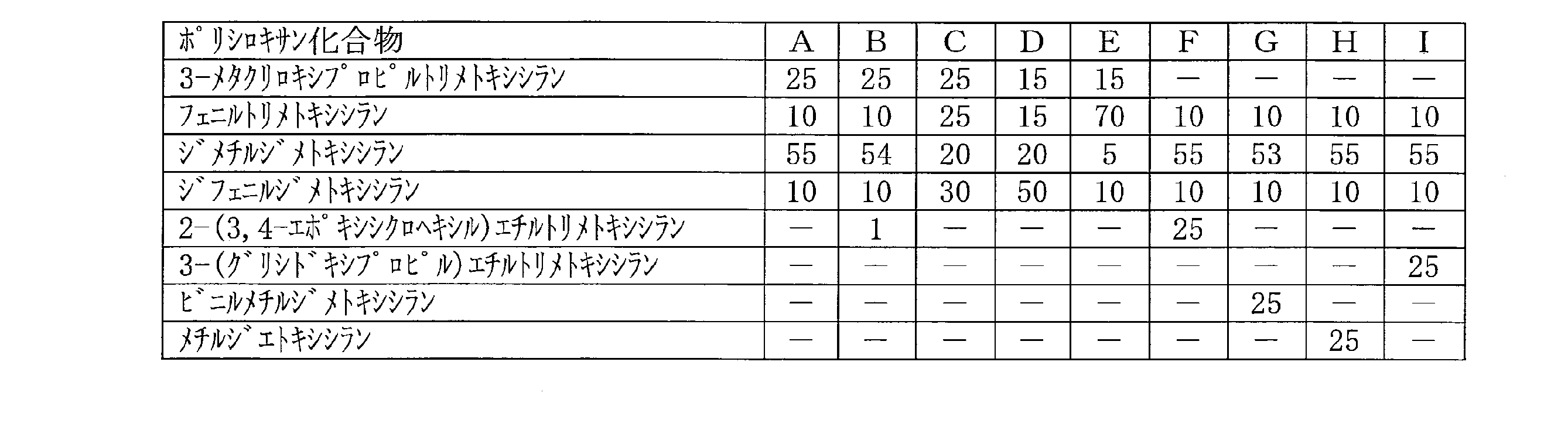
- Preparation Examples B to I Preparation of Polysiloxane Compounds B to I In Production Example A, except that the alkoxysilane compound shown in Table 1 was used, the same procedure as in Production Example A was performed, and polysiloxane compounds B to I shown in Table 1 were synthesized.
- the numerical values in the table represent the reaction molar ratio of the alkoxysilane compound.
- polysiloxane compounds A to E are the polysiloxane compounds of the present invention
- polysiloxane compounds F to I are comparative polysiloxane compounds.
- Table 2 shows the analysis results of mass average molecular weight and silanol group content.
- Photo radical generator 1 bis (2,6-dimethoxybenzoyl) phenyl phosphine oxide
- photo radical generator 2 bis (2,6-dimethoxybenzoyl) phenyl phosphine oxide
- photo radical generator 2 1-hydroxycyclohexyl phenyl ketone
- photo radical generator 2 [4- (2-chloro-4-benzoylphenylthio) phenylbis (4-chlorophenyl) sulfonium hexafluoroantimonate] as a photoacid generator, platinum as a hydrosilylation catalyst
- Photosensitive resin compositions or thermosetting resin compositions of Examples 1 to 7 and Comparative Examples 1 to 5 were prepared with the composition of Table 3 using divinyl tetramethyldisiloxane complex and butyl acetate as a solvent .
- the organic thin-film transistor as shown in FIG. 1 is produced as follows. did. Chromium (Cr) was vapor-deposited on the glass substrate 6 to form a lead electrode having a width of 2 mm and a thickness of about 100 nm.
- the photosensitive resin compositions of Examples 1 and 2 and Comparative Example 1 and the thermosetting resin composition of Comparative Example 2 are spin-coated thereon to a film thickness of about 1 ⁇ m and air-dried.
- the high-pressure mercury lamp was irradiated at 5000 mJ / cm 2
- the gate insulating film 5 was formed by curing by heating at 150 ° C. for 2 hours under a nitrogen atmosphere.
- a solution of poly- (3-hexyl) thiophene in xylene was spin-coated on the gate insulating film 5 so that the film thickness after drying was 30 nm, and air-dried to form an organic semiconductor film 1.
- Annealing treatment was performed at 150 ° C. for 30 minutes in a nitrogen atmosphere to activate poly- (3-hexyl) thiophene.
- Gold is vapor-deposited on the organic semiconductor film 1 to form a source electrode 2 and a drain electrode 3 with a channel width of 2 mm, a thickness of about 30 nm and a channel length of 100 ⁇ m. 12 bottom gate and top contact type organic thin film transistors were manufactured for each of and.
- the transport characteristics of the organic thin film transistors of Examples 1 and 2 and Comparative Examples 1 and 2 were measured using a semiconductor parameter analyzer (manufactured by Keithley, product name SCS 4200) to calculate charge mobility ⁇ .
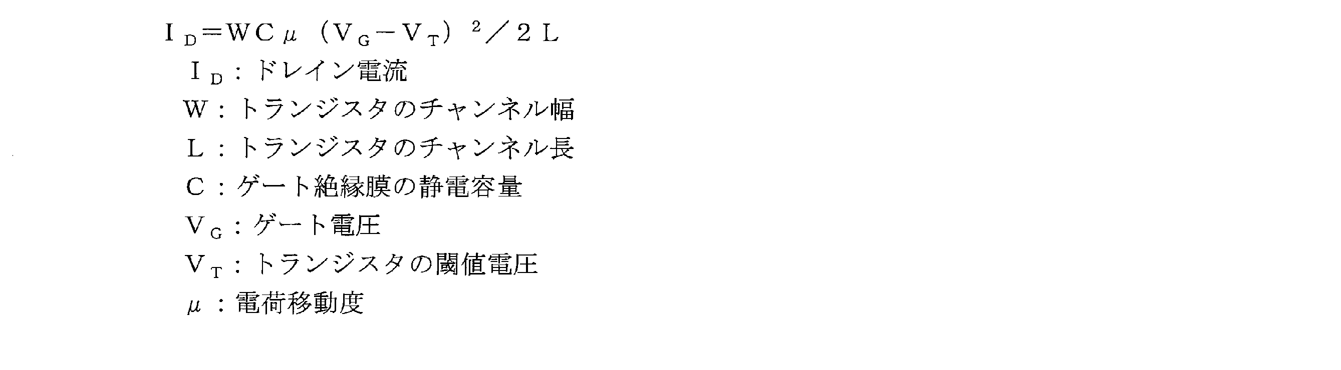
- the charge mobility ⁇ is defined by the following equation, and specifically, the graph in the saturation region when the square of the absolute value of the drain current I D is plotted on the vertical axis and the gate voltage V G is plotted on the horizontal axis.
- the charge mobility ⁇ was determined based on the slope.
- the measurement was performed under a nitrogen gas atmosphere and in a light shielding state.
- the charge mobility ⁇ was an average of the organic thin film transistors whose transport characteristics could be measured, and the number of the organic thin film transistors whose transport characteristics could not be measured due to current leakage was regarded as the number of defective products.
- the results are shown in Table 4.
- ⁇ Heat colorability evaluation of photosensitive resin composition The photosensitive resin compositions of Examples 3 to 7 and Comparative Examples 1 and 3 are applied by spin coating on a 2.5 cm square glass substrate so that the film thickness after drying is about 500 ⁇ m. The solvent was allowed to evaporate. The test piece was heat treated at 120 ° C. for 30 minutes. A photomask with a line width of 1 mm was placed on the top of the heat-treated glass substrate, and ultraviolet light was applied at 100 mJ / cm 2 with a high-pressure mercury lamp. Next, the test piece was immersed in a beaker containing ethyl acetate to dissolve and remove the uncured portion, and the air-dried one was used as a test piece for evaluation of heat colorability.
- the test pieces are all colorless and transparent, and the refractive index of the cured product at a wavelength of 837 nm is as shown in Table 6.
- the test piece was put in a thermostat at 150 ° C., taken out after 15 days, the coloration of the cured product was visually observed, and the heat colorability was evaluated according to the following evaluation criteria. The results are shown in Table 5.
- ⁇ Evaluation criteria> ⁇ : No coloring is observed, and heat coloring is low.
- ⁇ Slightly colored and slightly heat-colored.
- ⁇ Clearly colored and heat coloring is high.
- a gate insulating film obtained by curing the photosensitive resin composition of the present invention.
- a gate insulating film obtained by curing a photosensitive resin composition containing a polysiloxane compound having an epoxy group and a photoacid generator, a polysiloxane compound having a vinyl group, SiH
- the gate insulating film obtained by curing a thermosetting resin composition containing a polysiloxane compound having a hydroxyl group and a hydrosilylation catalyst (platinum catalyst)
- platinum catalyst platinum catalyst
- the photosensitive resin composition of the present invention can be used as a negative photoresist, and the cured product has a high refractive index and is thermally colored even at high temperatures. Is low (Examples 3 to 7).
- the cured products (Comparative Examples 1 and 3 to 5) obtained by curing a photosensitive resin composition having a different composition from the photosensitive resin composition of the present invention, the heat colorability is high. This shows that when the photosensitive resin composition of the present invention is used for a transparent high refractive index material such as a lens, an optical waveguide, etc., it can be used without losing transparency even at high temperatures. .
Landscapes
- Chemical & Material Sciences (AREA)
- Physics & Mathematics (AREA)
- Organic Chemistry (AREA)
- General Physics & Mathematics (AREA)
- Health & Medical Sciences (AREA)
- Chemical Kinetics & Catalysis (AREA)
- Medicinal Chemistry (AREA)
- Polymers & Plastics (AREA)
- Spectroscopy & Molecular Physics (AREA)
- Engineering & Computer Science (AREA)
- Metallurgy (AREA)
- Silicon Polymers (AREA)
- Materials For Photolithography (AREA)
- Macromonomer-Based Addition Polymer (AREA)
- Thin Film Transistor (AREA)
- Electroluminescent Light Sources (AREA)
Abstract
本発明は、フォトリソグラフィにより微細なパターンを形成でき、200℃を超える熱処理を行なわずに絶縁膜が形成でき、しかも有機薄膜トランジスタのゲート絶縁膜として使用した場合にキャリヤーがトラップされて電荷移動度が低下するという問題のない感光性樹脂組成物を提供するものであり、下記一般式(1)~(4)で表わされるユニットを有するポリシロキサン化合物及び光ラジカル発生剤を含有する感光性樹脂組成物を提供するものである。(式(1)中、R1は水素原子又はメチル基を表わし、R2は置換アルキル基を有していてもよい炭素数1~5のアルキレン基を表わし、式(2)中、R3は水素原子又は炭素数1~4のアルキル基を表わし、式(3)中、R4は炭素数1~6のアルキル基又は炭素数5~6のシクロアルキル基を表わし、式(4)中、R5は水素原子又は炭素数1~4のアルキル基を表わす。)
Description
本発明は、ポリシロキサン化合物を用いた感光性樹脂組成物に関し、更にこの感光性樹脂組成物を用いたネガ型フォトレジスト(特に永久レジスト)に関する。
近年、液晶表示装置、EL表示装置等の表示装置に関する研究が盛んに行われており、低消費電力で駆動可能な表示装置の一つとして電子ペーパーが注目されている。電子ペーパーは、紙のように厚さが薄く作ることが可能であり、低消費電力化や電源を切っても画像を保持できるという利点を有しており、電子書籍やポスターへの利用が期待されている。電子ペーパーの表示基板にプラスチックフィルムを使用し、表示装置の駆動部に有機薄膜トランジスタを使用すれば、柔軟で屈曲しても品質を損なわずに表示でき、応用範囲も広がり、普及が進むものと考えられている。
有機薄膜トランジスタのゲート絶縁膜は、一般に、炭化珪素、窒化珪素、酸化アルミニウム、酸化タンタル、酸化チタン等の絶縁性の高い無機系の材料を、CVD法により成膜して製造するが、CVD法は大掛かりな真空系装置を必要とすることから、製造コストの面で問題がある。また、これらの無機系の材料は硬質で剛直であり、プラスチックフィルム等のフレキシブルな基板に適用した場合には、屈曲により破損する恐れがある。
これに対し、有機系の材料は、有機溶媒に可溶なものが多いことから塗布法や印刷法により、安価に大量の製造が可能であり、また屈曲性やプラスチックフィルムへの密着性に優れることから、有機薄膜トランジスタのゲート絶縁膜用の有機絶縁材料の検討が盛んに行われている。
電子ペーパー等では微細な表示装置が必要であり、そこで用いられる有機薄膜トランジスタのゲート絶縁膜では微細なパターンの形成が求められる。微細なパターンの形成方法としては、フォトリソグラフィがあり、フォトリソグラフィによるゲート絶縁膜の形成が可能な感光性樹脂組成物としては、アルコキシシランの縮合物と光酸発生剤又は塩基発生剤とを含有する感光性樹脂組成物(例えば、特許文献1~3を参照)が知られている。
しかしながら、このような感光性樹脂組成物では、残存する光酸発生剤又は塩基発生剤及びそれらの分解物により電流リークが発生する場合がある。また感光性樹脂組成物を、アルコキシシリル基の架橋により硬化させるためには、200~500℃程度に熱処理する必要がある。このため、ポリカーボネート、ポリエチレンテレフタレート等のプラスチックフィルムを基板とすることができなかった。フォトリソグラフィが可能であり、絶縁性が高い絶縁膜が得られる感光性樹脂組成物としては、エポキシ基を有するポリシロキサン化合物と光酸発生剤とを含有する感光性樹脂組成物が知られているが、このような感光性樹脂組成物から得られる絶縁膜は、エポキシの開環により生成する水酸基により半導体層に形成されるキャリヤーがトラップされて電荷移動度が低下するという問題があった。
しかしながら、このような感光性樹脂組成物では、残存する光酸発生剤又は塩基発生剤及びそれらの分解物により電流リークが発生する場合がある。また感光性樹脂組成物を、アルコキシシリル基の架橋により硬化させるためには、200~500℃程度に熱処理する必要がある。このため、ポリカーボネート、ポリエチレンテレフタレート等のプラスチックフィルムを基板とすることができなかった。フォトリソグラフィが可能であり、絶縁性が高い絶縁膜が得られる感光性樹脂組成物としては、エポキシ基を有するポリシロキサン化合物と光酸発生剤とを含有する感光性樹脂組成物が知られているが、このような感光性樹脂組成物から得られる絶縁膜は、エポキシの開環により生成する水酸基により半導体層に形成されるキャリヤーがトラップされて電荷移動度が低下するという問題があった。
したがって、本発明の目的は、フォトリソグラフィにより微細なパターンが形成でき、200℃を超える熱処理を行なわずに絶縁膜が形成でき、しかも有機薄膜トランジスタのゲート絶縁膜として使用した場合にキャリヤーがトラップされて電荷移動度が低下するという問題のない感光性樹脂組成物を提供することにある。
本発明者は上記に鑑み鋭意研究の結果、本発明に到達した。即ち、本発明は、下記一般式(1)~(4)で表わされるユニットを有するポリシロキサン化合物、及び光ラジカル発生剤を含有する感光性樹脂組成物を提供するものである。

(式中、R1は水素原子又はメチル基を表わし、R2は置換アルキル基を有していてもよい炭素数1~5のアルキレン基を表わす。)

(式中、R3は水素原子又は炭素数1~4のアルキル基を表わす。)

(式中、R4は炭素数1~6のアルキル基又は炭素数5若しくは6のシクロアルキル基を表わす。)

(式中、R5は水素原子又は炭素数1~4のアルキル基を表わす。)
本発明の効果は、透明性が高いだけでなく、基板製作時の温度に耐えられる耐熱性及び耐溶剤性、更には永久レジストとしての耐経時変化性に優れた絶縁層を与えることの出来る感光性樹脂組成物(特にネガ型感光性樹脂組成物)、この感光性樹脂組成物を用いたネガ型フォトレジスト(特に永久レジスト)を提供したことにある。
以下、本発明について、好ましい実施形態に基づき詳細に説明する。
先ず、前記一般式(1)~(4)で表わされるユニットを有するポリシロキサン化合物(以下、本発明のポリシロキサン化合物という場合がある)について説明する。
先ず、前記一般式(1)~(4)で表わされるユニットを有するポリシロキサン化合物(以下、本発明のポリシロキサン化合物という場合がある)について説明する。
前記一般式(1)において、R1は水素原子又はメチル基を表わし、保存安定性が良好であることから、メチル基が好ましい。R2は置換アルキル基を有していてもよい炭素数1~5のアルキレン基を表わす。炭素数1~5のアルキレン基としては、メチレン、エチレン、プロピレン、ブチレン及びペンテンが挙げられ、耐熱性からは炭素数が少ないことが好ましいが、工業的な入手の容易さから、エチレン、プロピレン及びブチレンが好ましく、エチレン及びプロピレンが更に好ましく、プロピレンが最も好ましい。R2において有していてもよい置換アルキル基としては、例えば、メチル、エチル、プロピル、イソプロピル、ブチル、イソブチル、t-ブチル等が挙げられるが、耐熱性からは、置換アルキル基を有しないことが好ましい。
前記一般式(2)において、R3は水素原子又は炭素数1~4のアルキル基を表わし、炭素数1~4のアルキル基としては、メチル、エチル、プロピル、イソプロピル、ブチル、イソブチル、2級ブチル、t-ブチル等が挙げられる。R3としては、工業的な入手が容易であり、耐熱性が良好であることから、水素原子が好ましい。
前記一般式(3)において、R4は炭素数1~6のアルキル基又は炭素数5若しくは6のシクロアルキル基を表わす。炭素数1~6のアルキルとしては、メチル、エチル、プロピル、イソプロピル、ブチル、イソブチル、2級ブチル、t-ブチル、ペンチル、イソペンチル、ネオペンチル、2-ペンチル、t-ペンチル、ヘキシル、2-ヘキシル等が挙げられ、炭素数5若しくは6のシクロアルキル基としては、シクロペンチル、シクロヘキシル、メチルシクロペンチル、シクロペンチルメチル等が挙げられる。R4としては、耐熱性が良好であることから、エチル及びメチルが好ましく、メチルが更に好ましい。
前記一般式(4)において、R5は水素原子又は炭素数1~4のアルキル基を表わす。炭素数1~4のアルキル基としては、メチル、エチル、プロピル、イソプロピル、ブチル、イソブチル、2級ブチル、t-ブチル等が挙げられる。R5としては、工業的な入手が容易であり、耐熱性が良好であることから、水素原子が好ましい。
本発明のポリシロキサン化合物において、前記一般式(1)で表わされるユニットの含量は、0.1~5mmol/gであることが好ましく、0.5~3mmol/gであることが更に好ましく、1~2.5mmol/gであることが最も好ましい。前記一般式(2)で表わされるユニットの含量は、前記一般式(1)~(4)で表わされるユニットの数の合計に対して0.01~0.8であることが好ましく、0.03~0.5であることが更に好ましく、0.05~0.3であることが最も好ましい。前記一般式(3)で表わされるユニットの含量は、前記一般式(1)~(4)で表わされるユニットの数の合計に対して0.03~0.8であることが好ましく、0.07~0.7であることが更に好ましく、0.15~0.6であることが最も好ましい。前記一般式(4)で表わされるユニットの含量は、前記一般式(1)~(4)で表わされるユニットの数の合計に対して0.01~0.6であることが好ましく、0.03~0.4であることが更に好ましく、0.05~0.25であることが最も好ましい。
また、前記一般式(3)で表わされるユニットの数に対する、前記一般式(2)で表わされるユニットの数と前記一般式(4)で表わされるユニットの数の合計の比は、本発明の感光性樹脂組成物が用いられる用途により異なるが、ネガ型フォトレジストとして使用する場合には、0.3~5.0が好ましく、0.5~3が更に好ましく、1.5~2.5が最も好ましい。また、本発明の感光性樹脂組成物をレンズ、光導波路等の透明材料として使用する場合には、0.3~7.0が好ましく、0.3~5が更に好ましく、0.3~3が最も好ましい。
本発明のポリシロキサン化合物の分子量があまりに小さい場合には、本発明の感光性樹脂組成物の塗布性や成膜性が不十分となり、分子量があまりに大きい場合には、ハンドリング性が低下することから、本発明のポリシロキサン化合物は、質量平均分子量で1000~100000であることが好ましく、2000~50000であることが更に好ましく、3000~20000であることが最も好ましい。なお、本発明において、質量平均分子量とは、テトラヒドロフラン(以下、THFという)を溶媒としてGPC分析を行った場合のポリスチレン換算の質量平均分子量をいう。
本発明のポリシロキサン化合物は、その製法上、シラノール基(SiOH基)が残る場合があるが、シラノール基が存在することにより、本発明の感光性樹脂組成物の保存安定性が低下することから、本発明のポリシロキサン化合物中のシラノール基の含量は1.0mmol/g以下であることが好ましく、0.1mmol/g以下であることが更に好ましい。なお、シラノール基は、近赤外線分光光度計(特開2001-208683号公報、特開2003-35667号公報等を参照)や29Si-NMR(特開2007-217249公報等を参照)を使用した機器分析により定量することができる。シラノール基は、後述するようにハロシラン化合物や加水分解性エステルにより減少させることができる。
本発明のポリシロキサン化合物は、密着性が向上することから、更に下記一般式(5)で表わされるユニットを有することが好ましい。

前記一般式(5)において、Eはエポキシ基を有する基を表わし、エポキシ基を有する基としては、例えば、下記一般式(6)~(8)で表わされる基が挙げられ、密着性の向上効果が大きいことから、下記一般式(7)及び(8)で表わされる基が好ましく、下記一般式(7)で表わされる基が更に好ましい。



前記一般式(6)において、R6は置換アルキル基を有していてもよい炭素数1~5のアルキレン基を表わす。炭素数1~5のアルキレン基としては、メチレン、エチレン、プロピレン、ブチレン及びペンテンが挙げられ、耐熱性からは炭素数が少ないことが好ましいが、工業的な入手の容易さから、エチレン、プロピレン及びブチレンが好ましく、エチレン及びプロピレンが更に好ましく、エチレンが最も好ましい。R6において有していてもよい置換アルキル基としては、例えば、メチル、エチル、プロピル、イソプロピル、ブチル、イソブチル、t-ブチル等が挙げられるが、耐熱性からは、置換アルキル基を有しないことが好ましい。mは0又は1の数を表わし、原料の入手が容易であることから、mは1の数が好ましい。
前記一般式(7)において、R7は水素原子又はメチル基を表わし、R8は置換アルキル基を有していてもよい炭素数1~5のアルキレン基を表わす。炭素数1~5のアルキレン基としては、メチレン、エチレン、プロピレン、ブチレン及びペンテンが挙げられ、耐熱性からは炭素数が少ないことが好ましいが、工業的な入手の容易さから、エチレン、プロピレン及びブチレンが好ましく、エチレン及びプロピレンが更に好ましく、エチレンが最も好ましい。R8において有していてもよい置換アルキル基としては、例えば、メチル、エチル、プロピル、イソプロピル、ブチル、イソブチル、t-ブチル等が挙げられるが、耐熱性からは、置換アルキル基を有しないことが好ましい。nは0又は1の数を表わし、原料の入手が容易であることから、nは1の数が好ましい。
本発明のポリシロキサン化合物が更に、前記一般式(5)で表わされるユニットを有する場合、前記一般式(5)で表わされるユニットの含量があまりに少ない場合には、密着性の向上効果が少なく、またあまりに多い場合には、本発明の感光性樹脂組成物を硬化させた硬化物の表面にタックが出る場合があることから、前記一般式(5)で表わされるユニットの含量は、エポキシ当量で2000~50000であることが好ましく、3000~20000であることが好ましい。
本発明のポリシロキサン化合物は、下記一般式(1a)~(4a)で表わされるアルコキシシラン化合物又はハロシラン化合物の加水分解縮合反応、いわゆるゾルゲル反応により得ることができる。




前記一般式(1a)で表わされるアルコキシシラン化合物としては、例えば、(アクリロキシメチル)トリメトシキシシラン、(2-アクリロキシプロピル)トリメトシキシシラン、(3-アクリロキシプロピル)トリメトシキシシラン、(3-アクリロキシプロピル)トリエトシキシシラン、(メタクリロキシメチル)トリメトシキシシラン、(2-メタクリロキシプロピル)トリメトシキシシラン、(3-メタクリロキシプロピル)トリメトシキシシラン、(3-メタクリロキシプロピル)トリエトシキシシランが挙げられ、前記一般式(1a)で表わされるハロシラン化合物としては、例えば、3-アクリロキシプロピル)トリクロロシラン、(3-メタクリロキシプロピル)トリクロロシラン等が挙げられる。前記一般式(1a)で表わされるアルコキシシラン化合物又はハロシラン化合物としては、反応性が良好で反応の制御が容易であることから、(3-メタクリロキシプロピル)トリメトシキシシラン、及び(3-メタクリロキシプロピル)トリエトシキシシランが好ましく、(3-メタクリロキシプロピル)トリメトシキシシランが更に好ましい。
前記一般式(2a)で表わされるアルコキシシラン化合物としては、例えば、フェニルトリメトシキシシラン、フェニルトリエトシキシシラン、フェニルトリイソプロポキシシラン、4-メチルフェニルトリメトシキシシラン、4-メチルフェニルトリエトシキシシラン、4-メチルフェニルトリイソプロポキシシラン等が挙げられ、前記一般式(2a)で表わされるハロシラン化合物としては、例えば、フェニルトリクロロシラン、4-メチルフェニルトリクロロシラン等が挙げられる。前記一般式(2a)で表わされるアルコキシシラン化合物又はハロシラン化合物としては、反応性が良好で反応の制御が容易であることから、フェニルトリメトシキシシラン、及びフェニルトリエトシキシシランが好ましく、フェニルトリメトシキシシランが更に好ましい。
前記一般式(3a)で表わされるアルコキシシラン化合物としては、例えば、ジメチルジメトシキシシラン、ジメチルジエトシキシシラン、ジメチルジイソプロポキシシラン、ジエチルフェニルジメトシキシシラン、ジエチルジエトシキシシラン、ジエチルジイソプロポキシシラン、ジプロピルジメトシキシシラン、ジプロピルジエトシキシシラン、ジプロピルジイソプロポキシシラン等が挙げられ、前記一般式(3a)で表わされるハロシラン化合物としては、例えば、ジメチルジクロロシラン、ジエチルジクロロシラン、ジプロピルジクロロシラン等が挙げられる。前記一般式(2a)で表わされるアルコキシシラン化合物又はハロシラン化合物としては、反応性が良好で反応の制御が容易であることから、ジメチルジメトシキシシラン、及びジメチルジエトシキシシランが好ましく、ジメチルジメトシキシシランが更に好ましい。
前記一般式(4a)で表わされるアルコキシシラン化合物としては、例えば、ジフェニルジメトシキシシラン、ジフェニルジエトシキシシラン、ジフェニルジイソプロポキシシラン、ビス(4-メチルフェニル)ジメトシキシシラン、ビス(4-メチルフェニル)ジエトシキシシラン、ビス(4-メチルフェニル)ジイソプロポキシシラン等が挙げられ、前記一般式(4a)で表わされるハロシラン化合物としては、例えば、ジフェニルジクロロシラン、ビス(4-メチルフェニル)ジクロロシラン等が挙げられる。前記一般式(4a)で表わされるアルコキシシラン化合物又はハロシラン化合物としては、反応性が良好で反応の制御が容易であることから、ジフェニルジメトシキシシラン、及びジフェニルジエトシキシシランが好ましく、ジフェニルジメトシキシシランが更に好ましい。
前記一般式(1a)~(4a)で表わされるアルコキシシラン化合物又はハロシラン化合物を加水分解縮合する場合、溶媒中で、酸又は塩基等の触媒を使用して反応することが好ましい。反応に使用できる溶媒としては、水、メタノール、エタノール、n-プロパノール、イソプロパノール、n-ブタノール、イソブタノール、アセトン、メチルエチルケトン、ジオキサン、テトラヒドロフラン、トルエン、キシレン、シクロヘキサン等が挙げられ、これらの一種を用いることも二種以上を混合して用いることも出来る。水以外の溶媒を使用するためには、加水分解縮合反応を促進するために適量の水を添加して反応を行うことが好ましい。
アルコキシシラン化合物やハロシラン化合物の加水分解縮合反応では、アルコキシシリル基やハロシリル基が水によって加水分解しシラノール基が生成し、この生成したシラノール基同士、又はシラノール基とアルコキシル基若しくはクロロシラン基とが縮合してシロキサン基(SiOSi基)が生成する。
前記の加水分解縮合反応の触媒としては、塩酸、リン酸、硫酸等の無機酸類;ギ酸、酢酸、シュウ酸、クエン酸、メタンスルホン酸、ベンゼンスルホン酸、p-トルエンスルホン酸、リン酸モノイソプロピル等の有機酸類;水酸化ナトリウム、水酸化カリウム、水酸化リチウム、アンモニア等の無機塩基類;トリメチルアミン、トリエチルアミン、モノエタノールアミン、ジエタノールアミン等のアミン化合物(有機塩基)類等が挙げられ、これらの一種を用いることも、二種以上を併用することも出来る。加水分解縮合反応の温度は、溶媒の種類、触媒の種類及び量等により変わるが、0~80℃が好ましく、5~50℃が更に好ましく、8~30℃が最も好ましい。
前記一般式(1a)~(4a)で表わされるアルコキシシラン化合物又はハロシラン化合物を加水分解縮合する場合、それぞれのアルコキシシラン化合物又はハロシラン化合物を別々に反応させてもよいし、混合してから反応させてもよいが、反応物のバラツキが少なく安定して生産できることから、混合してから反応することが好ましい。
本発明のポリシロキサン化合物が更に、前記一般式(5)で表わされるユニットを有する場合は、前記一般式(1a)~(4a)で表わされるアルコキシシラン化合物又はハロシラン化合物に加えて、下記一般式(5a)で表わされるアルコキシシラン化合物又はハロシラン化合物を加水分解縮合すればよい。

前記一般式(5a)で表わされるアルコキシシラン化合物又はハロシラン化合物としては、例えば、3,4-エポキシブチルトリメトキシシラン、2-グリシドキシプロピルトリメトキシシラン、3-グリシドキシプロピルトリメトキシシラン、2-グリシドキシ-1-メチルエチルトリエトキシシラン、3-グリシドキシプロピルトリエトキシシラン、2-(3,4-エポキシシクロヘキシル)エチルトリメトキシシラン、2-(3,4-エポキシシクロヘキシル)エチルトリエトキシシラン、3,4-エポキシシクロヘキシルトリメトキシシラン、3,4-エポキシシクロヘキシルトリエトキシシラン、2-(3,4-エポキシ-4-メチルシクロヘキシル)プロピルトリメトキシシラン等が挙げられる。
本発明のポリシロキサン化合物を、アルコキシシラン化合物又はハロシラン化合物の加水分解縮合反応により得る場合には、製法上、シラノール基が残り、そのシラノール基が存在することにより、本発明の感光性樹脂組成物の保存安定性が低下することから、シラノール基を封止することが好ましい。シラノール基を封止する場合は、トリメチルクロロシラン、ヘキサメチルジシラザンによりトリメチルシリル化する方法、オルト蟻酸エステル、オルト酢酸エステル、テトラアルコキシメタン、炭酸エステル等の加水分解性エステル化合物によりアルコキシル化する方法等が挙げられる。
次に、光ラジカル発生剤について説明する。本発明において光ラジカル発生剤とは、エネルギー線照射によりラジカル重合を開始させることが可能な化合物をいい、エネルギー線としては、紫外線、電子線、X線、放射線、高周波等が挙げられる。光ラジカル発生剤としては、アセトフェノン系光ラジカル発生剤、ベンジル系光ラジカル発生剤、ベンゾフェノン系光ラジカル発生剤、チオキサントン系光ラジカル発生剤、アシルホスフィンオキサイド系光ラジカル発生剤等が挙げられる。光ラジカル発生剤は、1種のみを用いてもよく、2種以上を併用してもよい。
前記アセトフェノン系光ラジカル発生剤としては、例えば、ジエトキシアセトフェノン、2-ヒドロキシ-2-メチル-1-フェニルプロパン-1-オン、4’-イソプロピル-2-ヒドロキシ-2-メチルプロピオフェノン、2-ヒドロキシメチル-2-メチルプロピオフェノン、2,2-ジメトキシ-1,2-ジフェニルエタン-1-オン、p-ジメチルアミノアセトフェノン、p-ターシャリブチルジクロロアセトフェノン、p-ターシャリブチルトリクロロアセトフェノン、p-アジドベンザルアセトフェノン、1-ヒドロキシシクロヘキシルフェニルケトン、2-メチル-1-[4-(メチルチオ)フェニル]-2-モルフォリノプロパノン-1、2-ベンジル-2-ジメチルアミノ-1-(4-モルフォリノフェニル)-ブタノン-1、ベンゾイン、ベンゾインメチルエーテル、ベンゾインエチルエーテル、ベンゾインイソプロピルエーテル、ベンゾイン-n-ブチルエーテル、ベンゾインイソブチルエーテル、2-ヒドロキシ-2-メチル-1-[4-ビニル-(1-メチルビニル)フェニル]プロパノンのオリゴマー等が挙げられる。
前記ベンジル系光ラジカル発生剤としては、例えば、ジフェニルジケトン(ベンジルともいう)、ビス(4-メトキシフェニル)ジケトン(アニシルともいう)等が挙げられる。
前記ベンゾフェノン系光ラジカル発生剤としては、例えば、ベンゾフェノン、o-ベンゾイル安息香酸メチル、ミヒラーケトン、4,4’-ビスジエチルアミノベンゾフェノン、4,4’-ジクロロベンゾフェノン、4-ベンゾイル-4’-メチルジフェニルスルフィド等が挙げられる。
前記チオキサントン系光ラジカル発生剤としては、例えば、チオキサントン、2-メチルチオキサントン、2-エチルチオキサントン、2-クロロチオキサントン、2-イソプロピルチオキサントン、2,4-ジエチルチオオキサントン等が挙げられる。
前記アシルホスフィンオキサイド系光ラジカル発生剤としては、例えば、2-メチルベンゾイルジフェニルフォスフィンオキサイド、2,4,6-トリメチルベンゾイルジフェニルフォスフィンオキサイド、2,4,6-トリメチルベンゾイルフェニルフォスフィン酸メチルエステル等のモノアシルフォスフィンオキサイド系光ラジカル発生剤;ビス(2,6-ジメトキシベンゾイル)フェニルフォスフィンオキサイド、ビス(2,4,6-トリメチルベンゾイル)フェニルフォスフィンオキサイド、ビス(2,6-ジメトキシベンゾイル)-2,4,4-トリメチルペンチルフォスフィンオキサイド等のビスアシルフォスフィンオキサイド系光ラジカル発生剤があげられる。
本発明の感光性樹脂組成物を硬化させて有機薄膜トランジスタ用ゲート絶縁膜として用いる場合には、前記光ラジカル発生剤としては、高い電荷移動度が得られることから、アシルホスフィンオキサイド系光ラジカル発生剤が好ましく、モノアシルフォスフィンオキサイド系光ラジカル発生剤が更に好ましく、2,4,6-トリメチルベンゾイルジフェニルフォスフィンオキサイドが最も好ましい。2種以上の光ラジカル発生剤を併用する場合には、少なくとも1種がアシルホスフィンオキサイド系光ラジカル発生剤であることが好ましい。
また、本発明の感光性樹脂組成物を硬化させてレンズ、導波路等の透明材料として用いる場合には、前記光ラジカル発生剤としては、透明性の高い硬化物が得られることから、アセトフェノン系光ラジカル発生剤、及びアシルホスフィンオキサイド系光ラジカル発生剤が好ましく、アセトフェノン系光ラジカル発生剤が更に好ましく、1-ヒドロキシシクロヘキシルフェニルケトンが最も好ましい。2種以上の光ラジカル発生剤を併用する場合には、少なくとも1種がアセトフェノン系光ラジカル発生剤であることが好ましい。
本発明の感光性樹脂組成物中の光ラジカル発生剤の含有量は、光ラジカル発生剤の種類、本発明の感光性樹脂組成物中のラジカル重合性基の含有量、活性エネルギー線の種類と強度等により変わるが、本発明のポリシロキサン化合物100質量部に対して、0.1~10質量部であることが好ましく、0.2~7質量部であることが更に好ましく、0.3~5質量部であることが最も好ましい。前記光ラジカル発生剤の含有量が0.1質量部未満であると、硬化が不十分となる場合があり、10質量部を超えると、配合量に見合う増量効果が得られないばかりか、却って耐熱性、透明性等に悪影響を及ぼす場合がある。
本発明の感光性樹脂組成物は、更に、有機溶剤を含有してもよい。このような有機溶剤としては、例えば、ベンゼン、キシレン、トルエン、エチルベンゼン、スチレン、トリメチルベンゼン、ジエチルベンゼン、テトラヒドロナフタレン等の芳香族炭化水素化合物;ペンタン、イソペンタン、ヘキサン、イソヘキサン、ヘプタン、イソヘプタン、オクタン、イソオクタン、ノナン、イソノナン、デカン、イソデカン、イソドデカン、シクロヘキサン、メチルシクロヘキサン、メンタン、デカヒドロナフタレン等の飽和炭化水素化合物;ジエチルエーテル、ジプロピルエーテル、ジイソプロピルエーテル、ジブチルエーテル、ジエチレングリコールジメチルエーテル、ジエチレングリコールジエチルエーテル、テトラヒドロフラン、1,4-ジオキサン等のエーテル系溶媒;アセトン、メチルエチルケトン、メチルイソブチルケトン、ジエチルケトン、ジプロピルケトン、メチルアミルケトン、シクロヘキサノン等のケトン系溶媒;酢酸エチル、酢酸メチル、酢酸ブチル、酢酸プロピル、酢酸シクロヘキシル等のエステル系溶媒;プロピレングリコールモノメチルエーテルアセテート、エチレングリコールモノエチルエーテルアセテート、ジプロピレングリコールメチルエーテルアセテート、ジエチレングリコールモノエチルエーテルアセテート等のグリコールエステル系溶媒等が挙げられる。これらの溶剤は、単独あるいは2種類以上を組み合わせて用いることができる。
本発明の感光性樹脂組成物を塗布法や印刷法により使用する場合、上記有機溶剤の含有量は、本発明のポリシロキサン化合物100質量部に対して、5~200質量部であることが好ましく、10~100質量部であることが更に好ましい。
本発明の感光性樹脂組成物は、前記有機溶剤のほか、必要に応じて、光増感剤、可塑剤、チクソ性付与剤、光酸発生剤、熱酸発生剤、分散剤、消泡剤、顔料、染料等の任意成分を配合することができる。これらの任意成分の配合量は、本発明のポリシロキサン化合物100質量部に対して、合計で0.001~1質量部であることが好ましい。
本発明の感光性樹脂組成物は、基板等の対象物上に本発明の感光性樹脂組成物の層を形成した後に、活性エネルギー線を照射することにより硬化する。本発明の感光性樹脂組成物の層を形成する方法は、特に限定されず、例えば、浸漬塗工、フロー塗工、刷毛塗工、スプレー塗工、押出塗工、スピン塗工、ロール塗工、バー塗工等を使用することができ、スクリーン塗工やロール転写等の方法によればパターニングされた膜形成することができる。本発明の感光性樹脂組成物の層が形成される対象物としては、特に限定されず、用途に応じて、シリコン基板、ガラス基板、金属板、プラスチックス板等が用いられる。対象物上に形成される本発明の感光性樹脂組成物の層の厚さは、用途によって異なるが、半導体素子の絶縁膜や有機薄膜トランジスタのゲート絶縁膜として使用する場合は10nm~10μm、光導波路のコア部分として使用する場合は1~200μmが目安となる。
本発明の感光性樹脂組成物が有機溶剤を含有する場合は、本発明の感光性樹脂組成物の層を形成した後に、層中の有機溶剤を除去する目的で加熱処理(プリベークという場合がある)を行う。加熱処理の条件は、使用した有機溶剤の沸点や蒸気圧、本発明の感光性樹脂組成物の層の厚さ、層を形成した対象物の耐熱温度に応じて、適宜選択されるが、60~140℃で30秒~10分の加熱処理が目安となる。
感光性樹脂組成物の層に活性エネルギー線を照射する光源としては、超高圧水銀灯、DeepUVランプ、高圧水銀灯、低圧水銀灯、メタルハライドランプ、エキシマレーザー等が挙げられ、これらの光源は、光ラジカル発生剤や増感剤の感光波長に応じて適宜選択される。活性エネルギー線の照射エネルギーは、感光性樹脂組成物の層の厚さや光ラジカル発生剤の種類や使用量により適宜選択される。
活性エネルギー線を照射することにより感光性樹脂組成物の層が硬化するが、硬化物の層と基板等の対象物との密着性を向上させるために加熱処理(ポストベークという場合がある)をしてもよい。このような加熱処理は、好ましくは、窒素、ヘリウム、アルゴン等の不活性ガス雰囲気下に、60~200℃の温度で1分~2時間行うことが好ましい。
本発明の感光性樹脂組成物から得られる塗膜はフォトリソグラフィが可能であり、ネガ型フォトレジスト(特に永久レジスト)として使用することができる。本発明の感光性樹脂組成物をネガ型フォトレジストとして使用する場合は、本発明の感光性樹脂組成物を基板等に塗布して形成された塗膜に活性エネルギー線を照射する場合に、感光性樹脂組成物の塗膜をフォトマスクで被覆して活性エネルギー線を選択的に照射した後、遮光した部分(未硬化部分)を有機溶媒や現像液等に溶解・分散させて除去すること(現像という場合がある)により、パターニングされた硬化膜を形成することができる。遮光した部分を溶解・分散させる有機溶媒としは、例えば、アルカリ性水溶液、酸性水溶液、アセトン、メチルエチルケトン、メチルイソブチルケトン、エタノール、イソプロパノール、n―プロパノール、ベンゼン、プロピレングリコールモノメチルエーテル、プロピレングリコールモノメチルエーテルアセテート、酢酸エチル、酢酸ブチル、トルエン、o―キシレン、m-キシレン、p-キシレン、1,3,5-トリメチルベンゼン、1,3,4-トリメチルベンゼン等を挙げることができる。
本発明の感光性樹脂組成物により得られる硬化膜は、透明性、絶縁性、高屈折率、耐熱性、耐候性、耐薬品性等に優れることから、LED等の封止材料、光導波路、光学レンズ、半導体装置の絶縁膜として有用である。特に、トランジスタのゲート絶縁膜として使用した場合にキャリヤーがトラップされて電荷移動度が低下するという問題が少なく、有機薄膜トランジスタのゲート絶縁膜として極めて有用である。
以下に実施例及び比較例を挙げて、本発明を更に説明するが、本発明はこれらに限定されるものではない。
〔製造例A:ポリシロキサン化合物Aの製造〕
撹拌器、温度計及び還流器を有する反応容器に、3-メタクリロキシプロピルトリメトキシシラン124.2g(0.5モル)、フェニルトリメトキシシラン39.7g(0.2モル)、ジメチルジメトキシシラン132.2g(1.1モル)、ジフェニルジメトキシシラン75.3g(0.2モル)及び溶剤として1-ブタノール300gを仕込んだ。撹拌し、70℃まで加熱した後、0.12%リン酸水溶液100部を滴下し、更に80℃で1時間反応した。次いで水酸化ナトリウム水溶液を添加して反応液を中和後、80℃で1時間反応した。トルエン300gを添加した後、撹拌を停止して分離した水含有層を除去した。トルエン層を水1000gで3回水洗した後、窒素気流下、40℃で減圧して溶媒を留去した。これに、オルトギ酸トリエチル300gを添加し、130℃で1時間処理した後、窒素気流下、80℃で減圧して未反応オルトギ酸トリエチル等の揮発性成分を留去し、本発明のポリシロキサン化合物Aを得た。GPCによる分析の結果、質量平均分子量は7500であり、1H-NMRによる分析の結果、シラノール基は検出されなかった。
撹拌器、温度計及び還流器を有する反応容器に、3-メタクリロキシプロピルトリメトキシシラン124.2g(0.5モル)、フェニルトリメトキシシラン39.7g(0.2モル)、ジメチルジメトキシシラン132.2g(1.1モル)、ジフェニルジメトキシシラン75.3g(0.2モル)及び溶剤として1-ブタノール300gを仕込んだ。撹拌し、70℃まで加熱した後、0.12%リン酸水溶液100部を滴下し、更に80℃で1時間反応した。次いで水酸化ナトリウム水溶液を添加して反応液を中和後、80℃で1時間反応した。トルエン300gを添加した後、撹拌を停止して分離した水含有層を除去した。トルエン層を水1000gで3回水洗した後、窒素気流下、40℃で減圧して溶媒を留去した。これに、オルトギ酸トリエチル300gを添加し、130℃で1時間処理した後、窒素気流下、80℃で減圧して未反応オルトギ酸トリエチル等の揮発性成分を留去し、本発明のポリシロキサン化合物Aを得た。GPCによる分析の結果、質量平均分子量は7500であり、1H-NMRによる分析の結果、シラノール基は検出されなかった。
〔製造例B~I:ポリシロキサン化合物B~Iの製造〕
製造例Aにおいて、表1に示すアルコキシシラン化合物を用いる以外は製造例Aと同様の操作を行い、表1に示すポリシロキサン化合物B~Iを合成した。表中の数値は、アルコキシシラン化合物の反応モル比を表わす。表1のポリシロキサン化合物のうち、ポリシロキサン化合物A~Eは本発明のポリシロキサン化合物であり、ポリシロキサン化合物F~Iは比較のポリシロキサン化合物である。また、表2に、質量平均分子量及びシラノール基含量の分析結果を示す。
製造例Aにおいて、表1に示すアルコキシシラン化合物を用いる以外は製造例Aと同様の操作を行い、表1に示すポリシロキサン化合物B~Iを合成した。表中の数値は、アルコキシシラン化合物の反応モル比を表わす。表1のポリシロキサン化合物のうち、ポリシロキサン化合物A~Eは本発明のポリシロキサン化合物であり、ポリシロキサン化合物F~Iは比較のポリシロキサン化合物である。また、表2に、質量平均分子量及びシラノール基含量の分析結果を示す。

〔実施例1~7及び比較例1~5〕
ポリシロキサン化合物A~I、下記のアクリレートA及びB、光ラジカル発生剤としてビス(2,6-ジメトキシベンゾイル)フェニルフォスフィンオキサイド(以下、光ラジカル発生剤1とする)、1-ヒドロキシシクロヘキシルフェニルケトン(以下、光ラジカル発生剤2とする)、光酸発生剤として[4-(2-クロロ-4-ベンゾイルフェニルチオ)フェニルビス(4-クロロフェニル)スルホニウムヘキサフルオロアンチモネート]、ヒドロシリル化触媒として白金-ジビニルテトラメチルジシロキサン錯体、及び溶剤として酢酸ブチルを用い、表3の組成にて、実施例1~7及び比較例1~5の感光性樹脂組成物又は熱硬化性樹脂組成物を調製した。
ポリシロキサン化合物A~I、下記のアクリレートA及びB、光ラジカル発生剤としてビス(2,6-ジメトキシベンゾイル)フェニルフォスフィンオキサイド(以下、光ラジカル発生剤1とする)、1-ヒドロキシシクロヘキシルフェニルケトン(以下、光ラジカル発生剤2とする)、光酸発生剤として[4-(2-クロロ-4-ベンゾイルフェニルチオ)フェニルビス(4-クロロフェニル)スルホニウムヘキサフルオロアンチモネート]、ヒドロシリル化触媒として白金-ジビニルテトラメチルジシロキサン錯体、及び溶剤として酢酸ブチルを用い、表3の組成にて、実施例1~7及び比較例1~5の感光性樹脂組成物又は熱硬化性樹脂組成物を調製した。


<感光性樹脂組成物のゲート絶縁膜としての評価>
前記実施例及び比較例で得られた感光性樹脂組成物又は熱硬化性樹脂組成物のゲート絶縁膜としての特性を評価するために、図1に示すような有機薄膜トランジスタを次のようにして作製した。
ガラス基板6上に、クロム(Cr)を蒸着させ、幅2mm、厚さ約100nmの引き出し電極を形成しゲート電極4とした。この上に、実施例1、2及び比較例1の感光性樹脂組成物、並びに比較例2の熱硬化性樹脂組成物を膜厚が約1μmになるようにスピンコートし、風乾した後、実施例1及び2並びに比較例1では高圧水銀灯を5000mJ/cm2照射することにより、比較例2では窒素雰囲気下150℃で2時間加熱することにより硬化させてゲート絶縁膜5を形成した。ゲート絶縁膜5上に、ポリ-(3-ヘキシル)チオフェンのキシレン溶液を乾燥後の膜厚が30nmになるようにスピンコートし、風乾して有機半導体膜1を形成した。ポリ-(3-ヘキシル)チオフェンを活性化させるために窒素雰囲気下、150℃で30分アニール処理を行った。有機半導体膜1上に、金(Au)を蒸着させ、チャンネル幅2mm、厚さ約30nmでチャンネル長100μmのソース電極2とドレイン電極3を形成させることにより、実施例1及び2並びに比較例1及び2について、それぞれ12個のボトムゲート・トップコンタクト型の有機薄膜トランジスタを作製した。
前記実施例及び比較例で得られた感光性樹脂組成物又は熱硬化性樹脂組成物のゲート絶縁膜としての特性を評価するために、図1に示すような有機薄膜トランジスタを次のようにして作製した。
ガラス基板6上に、クロム(Cr)を蒸着させ、幅2mm、厚さ約100nmの引き出し電極を形成しゲート電極4とした。この上に、実施例1、2及び比較例1の感光性樹脂組成物、並びに比較例2の熱硬化性樹脂組成物を膜厚が約1μmになるようにスピンコートし、風乾した後、実施例1及び2並びに比較例1では高圧水銀灯を5000mJ/cm2照射することにより、比較例2では窒素雰囲気下150℃で2時間加熱することにより硬化させてゲート絶縁膜5を形成した。ゲート絶縁膜5上に、ポリ-(3-ヘキシル)チオフェンのキシレン溶液を乾燥後の膜厚が30nmになるようにスピンコートし、風乾して有機半導体膜1を形成した。ポリ-(3-ヘキシル)チオフェンを活性化させるために窒素雰囲気下、150℃で30分アニール処理を行った。有機半導体膜1上に、金(Au)を蒸着させ、チャンネル幅2mm、厚さ約30nmでチャンネル長100μmのソース電極2とドレイン電極3を形成させることにより、実施例1及び2並びに比較例1及び2について、それぞれ12個のボトムゲート・トップコンタクト型の有機薄膜トランジスタを作製した。
実施例1及び2並びに比較例1及び2の有機薄膜トランジスタについて、半導体パラメーターアナライザー(Keithley社製、製品名SCS4200)を用いて輸送特性を測定し、電荷移動度μを算出した。尚、電荷移動度μは下記の式で定義され、具体的には、ドレイン電流IDの絶対値の平方根を縦軸に、ゲート電圧VGを横軸にプロットしたときの飽和領域におけるグラフの傾きをもとに電荷移動度μを求めた。測定は、窒素ガス雰囲気下、遮光状態で行った。電荷移動度μは、輸送特性が測定ができた有機薄膜トランジスタの平均とし、電流リークにより輸送特性が測定できなかった有機薄膜トランジスタの数を不良品数とした。結果を表4に示す。

<感光性樹脂組成物の熱着色性評価>
2.5cm四方のガラス基板上に、実施例3~7並びに比較例1及び3~5の感光性樹脂性組成物を、乾燥後の膜厚が約500μmになるようにスピンコートにより塗布し、溶剤を揮発させた。この試験片を120℃で30分間加熱処理した。加熱処理後のガラス基板上部に線幅1mmが描かれたフォトマスクを設置し、高圧水銀灯により紫外線を100mJ/cm2で照射した。次に、この試験片を酢酸エチルを入れたビーカーに浸漬し、未硬化部分を溶解除去し、風乾したものを加熱着色性評価用の試験片として用いた。試験片はいずれも無色透明であり、硬化物の波長837nmにおける屈折率は表6に示すとおりである。この試験片を150℃の恒温槽に入れ、15日経過後に取り出し、硬化物の着色を目視し下記の評価基準で熱着色性を評価した。結果を表5に示す。
<評価基準>
◎:着色が見られず、熱着色性が低い。
○:わずかに着色しており熱着色性がやや高い。
△:明らかに着色しており熱着色性が高い。
×:硬化物を通して文字の線が判別できないほど着色しており熱着色性が非常に高い。
2.5cm四方のガラス基板上に、実施例3~7並びに比較例1及び3~5の感光性樹脂性組成物を、乾燥後の膜厚が約500μmになるようにスピンコートにより塗布し、溶剤を揮発させた。この試験片を120℃で30分間加熱処理した。加熱処理後のガラス基板上部に線幅1mmが描かれたフォトマスクを設置し、高圧水銀灯により紫外線を100mJ/cm2で照射した。次に、この試験片を酢酸エチルを入れたビーカーに浸漬し、未硬化部分を溶解除去し、風乾したものを加熱着色性評価用の試験片として用いた。試験片はいずれも無色透明であり、硬化物の波長837nmにおける屈折率は表6に示すとおりである。この試験片を150℃の恒温槽に入れ、15日経過後に取り出し、硬化物の着色を目視し下記の評価基準で熱着色性を評価した。結果を表5に示す。
<評価基準>
◎:着色が見られず、熱着色性が低い。
○:わずかに着色しており熱着色性がやや高い。
△:明らかに着色しており熱着色性が高い。
×:硬化物を通して文字の線が判別できないほど着色しており熱着色性が非常に高い。
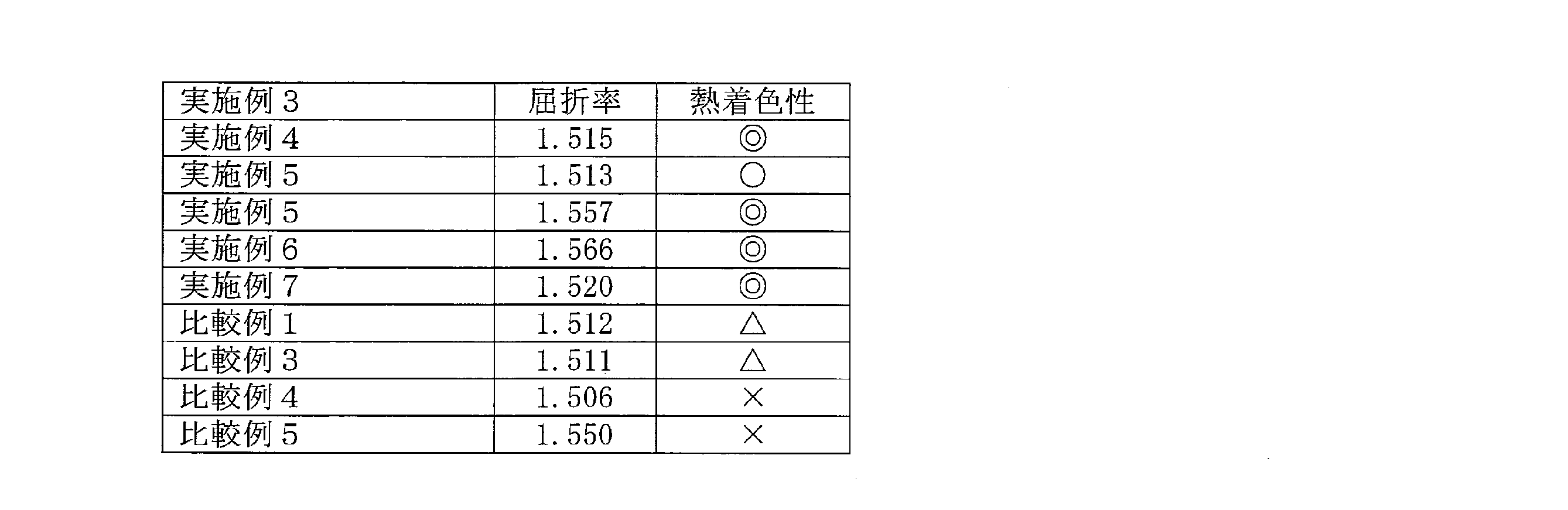
表4の結果が示すように、本発明の感光性樹脂組成物を硬化させて得られるゲート絶縁膜では、高い電荷移動度が得られる。これに対し、エポキシ基を有するポリシロキサン化合物と光酸発生剤とを含有する感光性樹脂組成物を硬化させて得られるゲート絶縁膜(比較例1)及び、ビニル基を有するポリシロキサン化合物、SiH基を有するポリシロキサン化合物及びヒドロシリル化触媒(白金触媒)を含有する熱硬化性樹脂組成物を硬化させて得られるゲート絶縁膜(比較例2)では、低い電荷移動度しか得られず、特に後者では不良品率が高いという問題がある。
また、表5の結果が示すように、本発明の感光性樹脂組成物は、ネガ型フォトレジストとして使用することが可能であり、その硬化物は、屈折率が高く、高温においても熱着色性が低い(実施例3~7)。これに対し、本願発明の感光性樹脂組成物とは組成が異なる感光性樹脂組成物を硬化させて得られる硬化物(比較例1及び3~5)では、熱着色性が高い。
これは、本発明の感光性樹脂組成物を、透明な高屈折率材料、例えばレンズ、光導波路等に使用した場合に、高温でも透明性を失わずに使用可能であることを示すものである。
これは、本発明の感光性樹脂組成物を、透明な高屈折率材料、例えばレンズ、光導波路等に使用した場合に、高温でも透明性を失わずに使用可能であることを示すものである。
1 有機半導体膜(層)
2 ソース電極
3 ドレイン電極
4 ゲート電極
5 絶縁層(ゲート絶縁膜)
6 支持体(基板)
2 ソース電極
3 ドレイン電極
4 ゲート電極
5 絶縁層(ゲート絶縁膜)
6 支持体(基板)
Claims (4)
- 下記一般式(1)~(4)で表わされるユニットを有するポリシロキサン化合物及び光ラジカル発生剤を含有する感光性樹脂組成物。




- 前記一般式(1)~(4)で表わされるユニットを有するポリシロキサン化合物が、更に下記一般式(5)で表わされるユニットを有するポリシロキサン化合物である、請求項1に記載の感光性樹脂組成物。

- 前記一般式(1)~(4)で表わされるユニットを有するポリシロキサン化合物が、下記一般式(1a)~(4a)で表わされるアルコキシシラン化合物又はハロシラン化合物を加水分解縮合して得られたポリシロキサン化合物である、請求項1に記載の感光性樹脂組成物。



- 前記一般式(1)~(4)で表わされるユニットを有するポリシロキサン化合物100質量部に対して、前記光ラジカル発生剤を0.1~10質量部含有する、請求項1~3の何れか1項に記載の感光性樹脂組成物。
Priority Applications (1)
| Application Number | Priority Date | Filing Date | Title |
|---|---|---|---|
| CN201180004535.0A CN102597879A (zh) | 2010-03-05 | 2011-03-04 | 感光性树脂组合物 |
Applications Claiming Priority (2)
| Application Number | Priority Date | Filing Date | Title |
|---|---|---|---|
| JP2010049437A JP2011186069A (ja) | 2010-03-05 | 2010-03-05 | 感光性樹脂組成物 |
| JP2010-049437 | 2010-03-05 |
Publications (1)
| Publication Number | Publication Date |
|---|---|
| WO2011108705A1 true WO2011108705A1 (ja) | 2011-09-09 |
Family
ID=44542349
Family Applications (1)
| Application Number | Title | Priority Date | Filing Date |
|---|---|---|---|
| PCT/JP2011/055074 Ceased WO2011108705A1 (ja) | 2010-03-05 | 2011-03-04 | 感光性樹脂組成物 |
Country Status (5)
| Country | Link |
|---|---|
| JP (1) | JP2011186069A (ja) |
| KR (1) | KR20110101073A (ja) |
| CN (1) | CN102597879A (ja) |
| TW (1) | TW201140243A (ja) |
| WO (1) | WO2011108705A1 (ja) |
Cited By (4)
| Publication number | Priority date | Publication date | Assignee | Title |
|---|---|---|---|---|
| JP2014082467A (ja) * | 2012-09-27 | 2014-05-08 | Dic Corp | 絶縁材料、絶縁膜及びこれを用いたトランジスタ |
| JP2015049492A (ja) * | 2013-09-04 | 2015-03-16 | Jsr株式会社 | ゲート絶縁膜、感放射線性樹脂組成物、硬化膜、ゲート絶縁膜の形成方法、半導体素子および表示装置 |
| JP2016086086A (ja) * | 2014-10-27 | 2016-05-19 | 住友化学株式会社 | 封止材組成物および光半導体素子 |
| JP2021521472A (ja) * | 2018-04-24 | 2021-08-26 | ダウ シリコーンズ コーポレーション | ポジ型光パターン形成が可能なシリコーン |
Families Citing this family (25)
| Publication number | Priority date | Publication date | Assignee | Title |
|---|---|---|---|---|
| WO2013031798A1 (ja) * | 2011-09-01 | 2013-03-07 | 東亞合成株式会社 | 耐熱衝撃性硬化物及びその製造方法 |
| JP2013092633A (ja) * | 2011-10-25 | 2013-05-16 | Adeka Corp | ポジ型感光性組成物 |
| JP5989417B2 (ja) * | 2012-06-20 | 2016-09-07 | モメンティブ・パフォーマンス・マテリアルズ・ジャパン合同会社 | 紫外線硬化型シリコーン樹脂組成物、及びそれを用いた画像表示装置 |
| JP6221279B2 (ja) * | 2013-03-18 | 2017-11-01 | 富士通株式会社 | レジスト組成物の製造方法及びパターン形成方法 |
| KR102232349B1 (ko) * | 2013-05-31 | 2021-03-26 | 롬엔드하스전자재료코리아유한회사 | 고내열성 네거티브형 감광성 수지 조성물 및 이로부터 제조된 경화막 |
| JP6184489B2 (ja) * | 2013-06-07 | 2017-08-23 | 富士フイルム株式会社 | ゲート絶縁膜形成用組成物、有機薄膜トランジスタ、電子ペーパー、ディスプレイデバイス |
| US9431619B2 (en) | 2013-09-27 | 2016-08-30 | Samsung Electronics Co., Ltd. | Composition for insulator, insulator, and thin film transistor |
| JP6167017B2 (ja) * | 2013-10-31 | 2017-07-19 | 富士フイルム株式会社 | 積層体、有機半導体製造用キットおよび有機半導体製造用レジスト組成物 |
| US10522771B2 (en) | 2014-12-01 | 2019-12-31 | Samsung Electronics Co., Ltd. | Composition, electronic device, and thin film transistor |
| KR102407114B1 (ko) | 2015-05-29 | 2022-06-08 | 삼성전자주식회사 | 절연액, 절연체, 박막 트랜지스터 및 전자 소자 |
| TWI597574B (zh) * | 2015-08-19 | 2017-09-01 | 奇美實業股份有限公司 | 感光性樹脂組成物及其應用 |
| KR102380151B1 (ko) | 2015-08-31 | 2022-03-28 | 삼성전자주식회사 | 박막 트랜지스터, 및 이를 포함하는 전자 장치 |
| EP3432375B1 (en) | 2016-03-16 | 2021-12-29 | FUJIFILM Corporation | Organic semiconductor composition, method for manufacturing organic thin film transistor, and organic thin film transistor |
| WO2017170279A1 (ja) | 2016-04-01 | 2017-10-05 | 富士フイルム株式会社 | 有機半導体素子、重合体、有機半導体組成物及び有機半導体膜 |
| JP6574052B2 (ja) | 2016-04-01 | 2019-09-11 | 富士フイルム株式会社 | 有機半導体素子、重合体、有機半導体組成物及び有機半導体膜 |
| CN109791983B (zh) | 2016-09-29 | 2023-06-16 | 富士胶片株式会社 | 微晶有机半导体膜、有机半导体晶体管及其制造方法 |
| WO2018061821A1 (ja) | 2016-09-29 | 2018-04-05 | 富士フイルム株式会社 | 有機半導体膜形成用組成物、有機半導体膜及びその製造方法、並びに、有機半導体素子 |
| WO2018181054A1 (ja) | 2017-03-31 | 2018-10-04 | 富士フイルム株式会社 | 有機半導体素子、有機半導体組成物、有機半導体膜の製造方法、有機半導体膜、並びに、これらに用いる化合物及びポリマー |
| JP6752466B2 (ja) | 2017-03-31 | 2020-09-09 | 富士フイルム株式会社 | 有機半導体素子、有機半導体組成物、有機半導体膜の製造方法、有機半導体膜、並びに、これらに用いる化合物及びポリマー |
| EP3605630B1 (en) | 2017-03-31 | 2020-12-23 | FUJIFILM Corporation | Organic semiconductor element, organic semiconductor composition, method of manufacturing organic semiconductor film, organic semiconductor film, and compound and polymer using for use therein |
| SG11202001261SA (en) * | 2017-08-24 | 2020-03-30 | Dow Global Technologies Llc | Method for optical waveguide fabrication |
| JP7206912B2 (ja) * | 2017-09-29 | 2023-01-18 | 東レ株式会社 | 電界効果型トランジスタ、その製造方法、それを用いた無線通信装置および商品タグ |
| CN109541889B (zh) * | 2018-12-19 | 2020-06-26 | 江苏艾森半导体材料股份有限公司 | 用于半导体封装工艺的负性光刻胶 |
| WO2022202499A1 (ja) * | 2021-03-26 | 2022-09-29 | ダウ・東レ株式会社 | 紫外線硬化性組成物およびその用途 |
| JP2024161834A (ja) | 2023-05-08 | 2024-11-20 | 学校法人東京理科大学 | 硬化性組成物 |
Citations (2)
| Publication number | Priority date | Publication date | Assignee | Title |
|---|---|---|---|---|
| JPS53134085A (en) * | 1977-07-18 | 1978-11-22 | Dainippon Printing Co Ltd | Photopolymerizable composition |
| JP2010039056A (ja) * | 2008-08-01 | 2010-02-18 | Sekisui Chem Co Ltd | 感光性組成物及びパターン膜の製造方法 |
-
2010
- 2010-03-05 JP JP2010049437A patent/JP2011186069A/ja active Pending
-
2011
- 2011-03-03 TW TW100107208A patent/TW201140243A/zh unknown
- 2011-03-04 CN CN201180004535.0A patent/CN102597879A/zh active Pending
- 2011-03-04 WO PCT/JP2011/055074 patent/WO2011108705A1/ja not_active Ceased
- 2011-03-04 KR KR1020110019235A patent/KR20110101073A/ko not_active Withdrawn
Patent Citations (2)
| Publication number | Priority date | Publication date | Assignee | Title |
|---|---|---|---|---|
| JPS53134085A (en) * | 1977-07-18 | 1978-11-22 | Dainippon Printing Co Ltd | Photopolymerizable composition |
| JP2010039056A (ja) * | 2008-08-01 | 2010-02-18 | Sekisui Chem Co Ltd | 感光性組成物及びパターン膜の製造方法 |
Cited By (5)
| Publication number | Priority date | Publication date | Assignee | Title |
|---|---|---|---|---|
| JP2014082467A (ja) * | 2012-09-27 | 2014-05-08 | Dic Corp | 絶縁材料、絶縁膜及びこれを用いたトランジスタ |
| JP2015049492A (ja) * | 2013-09-04 | 2015-03-16 | Jsr株式会社 | ゲート絶縁膜、感放射線性樹脂組成物、硬化膜、ゲート絶縁膜の形成方法、半導体素子および表示装置 |
| JP2016086086A (ja) * | 2014-10-27 | 2016-05-19 | 住友化学株式会社 | 封止材組成物および光半導体素子 |
| JP2021521472A (ja) * | 2018-04-24 | 2021-08-26 | ダウ シリコーンズ コーポレーション | ポジ型光パターン形成が可能なシリコーン |
| JP7307090B2 (ja) | 2018-04-24 | 2023-07-11 | ダウ シリコーンズ コーポレーション | ポジ型光パターン形成が可能なシリコーン |
Also Published As
| Publication number | Publication date |
|---|---|
| KR20110101073A (ko) | 2011-09-15 |
| CN102597879A (zh) | 2012-07-18 |
| JP2011186069A (ja) | 2011-09-22 |
| TW201140243A (en) | 2011-11-16 |
Similar Documents
| Publication | Publication Date | Title |
|---|---|---|
| JP2011186069A (ja) | 感光性樹脂組成物 | |
| US11634610B2 (en) | Siloxane polymer compositions and their use | |
| KR101805191B1 (ko) | 실페닐렌 함유 광 경화성 조성물, 그것을 사용한 패턴 형성 방법 및 그 방법에 의해 얻어지는 광 반도체 소자 | |
| JP5459315B2 (ja) | シランカップリング剤、ネガ型感光性樹脂組成物、硬化膜、およびタッチパネル用部材 | |
| CN103995437B (zh) | 负型感光性硅氧烷组合物 | |
| TWI877121B (zh) | 樹脂組合物、感光性樹脂組合物、硬化膜、硬化膜之製造方法、圖案硬化膜及圖案硬化膜之製作方法 | |
| CN104115067B (zh) | 负型感光性树脂组合物、固化膜以及触摸面板用构件 | |
| KR102493962B1 (ko) | 감광성 수지 조성물 및 이로부터 제조된 경화막 | |
| CN105629663B (zh) | 感光性树脂组合物 | |
| CN105764993A (zh) | 含硅的热或光固化性组合物 | |
| KR101589165B1 (ko) | 실란계 조성물 및 그 경화막, 및 그것을 이용한 네거티브형 레지스트 패턴의 형성 방법 | |
| KR101799361B1 (ko) | 감광성 수지 조성물 | |
| KR20200060466A (ko) | 포지티브형 감광성 실록산 조성물 및 이를 사용하는 경화 막 | |
| CN105652593B (zh) | 感光性树脂组合物和由其制备的固化膜 | |
| JP2019189803A (ja) | アミック酸基含有ポリシロキサンの製造方法、オルガノポリシロキサン、アミック酸基含有樹脂組成物、硬化膜、半導体装置、及び電子部品の製造方法 | |
| JP6883946B2 (ja) | 積層体及びその製造方法並びに基板の接着方法 | |
| TWI609927B (zh) | 含有機聚矽氧烷之可固化樹脂組成物 | |
| KR20140058847A (ko) | 유무기 복합 실록산계 고분자 및 이를 포함하는 포지티브형 감광성 수지 조성물 | |
| JP6048066B2 (ja) | ビフェニル骨格を含有するポリシロキサン及び被膜形成用組成物 | |
| KR20180037888A (ko) | 감광성 수지 조성물 및 이로부터 제조된 경화막 | |
| JP6799372B2 (ja) | ネガ型感光性組成物 | |
| WO2026105567A1 (ja) | 分岐状オルガノポリシロキサン、硬化性組成物、及びそれらの用途 | |
| TW202515941A (zh) | 含有支鏈狀有機聚矽氧烷之組成物及其用途 | |
| WO2026105566A1 (ja) | 分岐状オルガノポリシロキサン、硬化性組成物、及びそれらの用途 | |
| US20260098128A1 (en) | Curable branched organopolysiloxane, high energy ray-curable composition containing same, and use thereof |
Legal Events
| Date | Code | Title | Description |
|---|---|---|---|
| WWE | Wipo information: entry into national phase |
Ref document number: 201180004535.0 Country of ref document: CN |
|
| 121 | Ep: the epo has been informed by wipo that ep was designated in this application |
Ref document number: 11750814 Country of ref document: EP Kind code of ref document: A1 |
|
| NENP | Non-entry into the national phase |
Ref country code: DE |
|
| 122 | Ep: pct application non-entry in european phase |
Ref document number: 11750814 Country of ref document: EP Kind code of ref document: A1 |