WO2011108309A1 - 発光装置、発光装置の製造方法、照明装置およびバックライト - Google Patents
発光装置、発光装置の製造方法、照明装置およびバックライト Download PDFInfo
- Publication number
- WO2011108309A1 WO2011108309A1 PCT/JP2011/051318 JP2011051318W WO2011108309A1 WO 2011108309 A1 WO2011108309 A1 WO 2011108309A1 JP 2011051318 W JP2011051318 W JP 2011051318W WO 2011108309 A1 WO2011108309 A1 WO 2011108309A1
- Authority
- WO
- WIPO (PCT)
- Prior art keywords
- light emitting
- light
- substrate
- emitting device
- rod
- Prior art date
- Legal status (The legal status is an assumption and is not a legal conclusion. Google has not performed a legal analysis and makes no representation as to the accuracy of the status listed.)
- Ceased
Links
Images























Classifications
-
- H—ELECTRICITY
- H10—SEMICONDUCTOR DEVICES; ELECTRIC SOLID-STATE DEVICES NOT OTHERWISE PROVIDED FOR
- H10H—INORGANIC LIGHT-EMITTING SEMICONDUCTOR DEVICES HAVING POTENTIAL BARRIERS
- H10H20/00—Individual inorganic light-emitting semiconductor devices having potential barriers, e.g. light-emitting diodes [LED]
- H10H20/80—Constructional details
- H10H20/85—Packages
-
- H—ELECTRICITY
- H10—SEMICONDUCTOR DEVICES; ELECTRIC SOLID-STATE DEVICES NOT OTHERWISE PROVIDED FOR
- H10W—GENERIC PACKAGES, INTERCONNECTIONS, CONNECTORS OR OTHER CONSTRUCTIONAL DETAILS OF DEVICES COVERED BY CLASS H10
- H10W90/00—Package configurations
-
- H—ELECTRICITY
- H10—SEMICONDUCTOR DEVICES; ELECTRIC SOLID-STATE DEVICES NOT OTHERWISE PROVIDED FOR
- H10H—INORGANIC LIGHT-EMITTING SEMICONDUCTOR DEVICES HAVING POTENTIAL BARRIERS
- H10H20/00—Individual inorganic light-emitting semiconductor devices having potential barriers, e.g. light-emitting diodes [LED]
- H10H20/80—Constructional details
- H10H20/81—Bodies
-
- H—ELECTRICITY
- H10—SEMICONDUCTOR DEVICES; ELECTRIC SOLID-STATE DEVICES NOT OTHERWISE PROVIDED FOR
- H10H—INORGANIC LIGHT-EMITTING SEMICONDUCTOR DEVICES HAVING POTENTIAL BARRIERS
- H10H20/00—Individual inorganic light-emitting semiconductor devices having potential barriers, e.g. light-emitting diodes [LED]
- H10H20/80—Constructional details
- H10H20/81—Bodies
- H10H20/811—Bodies having quantum effect structures or superlattices, e.g. tunnel junctions
- H10H20/812—Bodies having quantum effect structures or superlattices, e.g. tunnel junctions within the light-emitting regions, e.g. having quantum confinement structures
-
- H—ELECTRICITY
- H10—SEMICONDUCTOR DEVICES; ELECTRIC SOLID-STATE DEVICES NOT OTHERWISE PROVIDED FOR
- H10H—INORGANIC LIGHT-EMITTING SEMICONDUCTOR DEVICES HAVING POTENTIAL BARRIERS
- H10H20/00—Individual inorganic light-emitting semiconductor devices having potential barriers, e.g. light-emitting diodes [LED]
- H10H20/80—Constructional details
- H10H20/81—Bodies
- H10H20/819—Bodies characterised by their shape, e.g. curved or truncated substrates
- H10H20/821—Bodies characterised by their shape, e.g. curved or truncated substrates of the light-emitting regions, e.g. non-planar junctions
-
- H—ELECTRICITY
- H10—SEMICONDUCTOR DEVICES; ELECTRIC SOLID-STATE DEVICES NOT OTHERWISE PROVIDED FOR
- H10W—GENERIC PACKAGES, INTERCONNECTIONS, CONNECTORS OR OTHER CONSTRUCTIONAL DETAILS OF DEVICES COVERED BY CLASS H10
- H10W72/00—Interconnections or connectors in packages
- H10W72/071—Connecting or disconnecting
- H10W72/075—Connecting or disconnecting of bond wires
- H10W72/07551—Connecting or disconnecting of bond wires characterised by changes in properties of the bond wires during the connecting
- H10W72/07554—Connecting or disconnecting of bond wires characterised by changes in properties of the bond wires during the connecting changes in dispositions
-
- H—ELECTRICITY
- H10—SEMICONDUCTOR DEVICES; ELECTRIC SOLID-STATE DEVICES NOT OTHERWISE PROVIDED FOR
- H10W—GENERIC PACKAGES, INTERCONNECTIONS, CONNECTORS OR OTHER CONSTRUCTIONAL DETAILS OF DEVICES COVERED BY CLASS H10
- H10W72/00—Interconnections or connectors in packages
- H10W72/50—Bond wires
- H10W72/541—Dispositions of bond wires
- H10W72/547—Dispositions of multiple bond wires
-
- H—ELECTRICITY
- H10—SEMICONDUCTOR DEVICES; ELECTRIC SOLID-STATE DEVICES NOT OTHERWISE PROVIDED FOR
- H10W—GENERIC PACKAGES, INTERCONNECTIONS, CONNECTORS OR OTHER CONSTRUCTIONAL DETAILS OF DEVICES COVERED BY CLASS H10
- H10W72/00—Interconnections or connectors in packages
- H10W72/851—Dispositions of multiple connectors or interconnections
- H10W72/874—On different surfaces
- H10W72/884—Die-attach connectors and bond wires
Definitions
- the present invention relates to a light emitting device, a method for manufacturing the light emitting device, a lighting device, and a backlight.
- LED chips 710 are mounted on a package substrate 700 on which a lead frame 701 is mounted, and an n-type electrode 705 of the LED chip 710 After the p-type electrode 706 is connected to the lead frame 701 by bonding wires 711 and 712, the LED chip 710 surrounded by the reflector 721 is filled with a resin 722 containing a phosphor, and further the resin 722 containing the phosphor. Some of them are filled with a transparent resin 723 (see, for example, Non-Patent Document 1).
- a semiconductor layer 703 made of GaN is stacked on a sapphire substrate 702, and the semiconductor layer 703 has an active layer 704.
- the size of the LED chip is sufficiently larger than the thickness (for example, 100 ⁇ m) of the thermally conductive substrate 801 that functions to efficiently release heat from the LED chip.
- the thermally conductive substrate 801 is a metal film or a metal film coated with an insulating film.
- the heat conductive substrate 801 is allowed to flow out heat in the lateral direction, so that the amount of heat outflow increases.
- the central region is hotter than the peripheral portion, so the temperature of the active layer rises and the light emission efficiency decreases, or a transparent resin that is close.
- the phosphor is deteriorated and the life is shortened.
- the variation in the brightness for each LED chip becomes the variation in the brightness of the light emitting device as it is, so that the yield of the light emitting device is poor. There is.
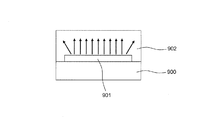
- the light flux concentrates on the region of the LED chip 901 mounted on the substrate 900, and therefore the resin 902 covering the LED chip 901 deteriorates and the light emission efficiency is increased. There is a problem that the service life is shortened and the lifetime is shortened (the thermally conductive substrate is omitted in FIG. 39).
- Motomura Murakami “13th Transition of Semiconductor Package Technology for LED / LD”, SemiconductoremiFPD World, Press Journal, May 2009, p. 114-117 ( Figure 5)
- an object of the present invention is to provide a light emitting device capable of realizing a long lifetime and high efficiency by dispersing light emission while suppressing temperature rise during light emission, and a method for manufacturing the light emitting device Is to provide.
- Another object of the present invention is to provide an illuminating device in which brightness variation is small and a long life and high efficiency can be realized by using the light emitting device.
- Another object of the present invention is to provide a backlight capable of realizing long life and high efficiency with less variation in brightness by using the light emitting device.
- a light-emitting device of the present invention includes: A plurality of light emitting elements each having an area of a light emitting surface of 2500 ⁇ m 2 or less are arranged on the mounting surface of the same substrate.
- the plurality of light emitting elements are not limited to light emitting elements having a flat light emitting surface such as a circular shape, an elliptical shape, a square shape, a rectangular shape, or a polygonal shape, but may be curved surfaces such as a cylindrical shape, a bowl shape, and a hemispherical shape.
- a light-emitting element having a formed light-emitting surface may be used.
- the plurality of light emitting elements may be in direct contact with the substrate, or may be in contact with the substrate via a thermal conductor, and light emitting elements that are in contact with both may be combined.
- the light emitting elements are in direct contact with the substrate (or heat In the state of being indirectly contacted via the conductor), the heat flow in the lateral direction to the substrate side is also performed at the central portion of the light emitting surface, and the temperature of the light emitting element is lowered including the central portion of the light emitting surface. Therefore, the temperature rise at the time of light emission is suppressed. Then, by arranging 100 or more such light emitting elements on the mounting surface of the same substrate, it is possible to reduce the entire brightness variation when a plurality of light emitting elements having brightness variations are assembled into one light emission.
- the amount of decrease in luminous efficiency due to the temperature rise of the light emitting element varies from element to element, the temperature rise is suppressed by making the area of the light emitting surface per light emitting element not more than 2500 ⁇ m 2 , and the light emitting efficiency is reduced. Since variation in the amount of decrease is suppressed, the effect of reducing brightness variation by using 100 or more fine light emitting elements is further enhanced. Furthermore, by miniaturizing the light emitting elements and arranging them dispersed on the same substrate, for example, a light amount equivalent to that of one light emitting element can be obtained with a plurality of fine light emitting elements, and the light irradiated to the resin is dispersed.
- the light intensity can be weakened, and the life can be extended by suppressing the deterioration of the resin.
- dispersing light emission while suppressing temperature rise during light emission there is little variation in brightness, and a longer life and higher efficiency can be realized.
- the area of the light emitting surface per light emitting element is 625 ⁇ m 2 or less.
- the area of the mounting surface of the substrate is at least four times the total light emitting area of the plurality of light emitting elements,
- the plurality of light emitting elements are arranged substantially evenly distributed on the mounting surface of the substrate.
- the plurality of light emitting elements are arranged on the mounting surface of the substrate having an area that is four times or more the sum of the light emitting areas of the plurality of light emitting elements, so that light is emitted by light emission. Since the heat generated in the element is efficiently discharged laterally to the substrate side and the temperature distribution becomes uniform, the temperature rise during light emission is further suppressed, and the lifetime and efficiency can be further improved.
- a light emitting element 910 having a light emitting surface of a flat square (one side length a) having an area of a light emitting surface of 2500 ⁇ m 2 or less is a square.
- the area of the substrate 900 occupied by one light emitting element 910 is four times (4a 2 ) with respect to the light emitting area (a 2 ) of one light emitting element 910, the conventional light emitting element shown in FIG.
- the light intensity of the light emitting element 910 is dispersed by ensuring the sufficient distance between the light emitting elements 910 adjacent to each other. The deterioration of the resin 912 can be suppressed.
- the plurality of light emitting elements are rod-shaped, The plurality of light emitting elements are arranged on the mounting surface of the substrate so that the longitudinal direction of the plurality of light emitting elements is parallel to the mounting surface of the substrate.
- the embodiment by arranging the plurality of light emitting elements on the mounting surface of the substrate so that the longitudinal direction of the plurality of rod-shaped light emitting elements is parallel to the mounting surface of the substrate, Since the ratio of the length in the axial direction (longitudinal direction) can be increased, the heat flow in the lateral direction to the substrate side is more efficient when the area of the light emitting surface of the light emitting element is the same than when the light emitting surface is a flat square. As a result, the temperature rise at the time of light emission is further suppressed, and a longer life and higher efficiency can be achieved.
- the rod-shaped light emitting element has a cylindrical light emitting surface that concentrically surrounds a rod-shaped core.
- the rod-shaped light emitting element has a cylindrical light emitting surface concentrically surrounding the rod-shaped core, whereby a plurality of light emitting elements each having an area of the light emitting surface of 2500 ⁇ m 2 or less. As long as 100 or more are arranged on the mounting surface of the same substrate, the area of the light emitting surface per light emitting element increases, and the number of light emitting elements for obtaining a predetermined brightness is reduced. Can reduce costs.
- the plurality of light emitting elements are light emitting diodes, The plurality of light emitting diodes are connected between a first electrode and a second electrode formed on the substrate at a predetermined interval, The plurality of light emitting diodes include a light emitting diode having an anode connected to the first electrode and a cathode connected to the second electrode, and a cathode connected to the first electrode and the second electrode.
- a light emitting diode having an anode connected to an electrode is mixed and disposed on the substrate, The plurality of light emitting diodes are driven by applying an AC voltage between the first electrode and the second electrode by an AC power source.
- the process can be simplified.
- the process of aligning the polarities (directions) of the plurality of light emitting diodes is not required at the time of manufacture, thus simplifying the process.
- the manufacturing process of the light emitting diode can be simplified and the manufacturing cost can be suppressed. Note that when the size of the light emitting diode is small or the number of light emitting diodes is large, the above manufacturing process can be greatly simplified as compared with the case where the light emitting diodes are arranged with the same polarity.
- substrate is attached on the heat sink.
- the heat radiation effect is further improved by mounting the substrate on the heat sink.
- a substrate having at least the first electrode and the second electrode on the mounting surface is prepared, and a liquid containing a plurality of fine light-emitting elements is applied on the substrate. Thereafter, a voltage is applied to at least the first electrode and the second electrode, and a plurality of fine light-emitting elements are arranged at positions defined by at least the first electrode and the second electrode. Accordingly, the plurality of light emitting elements can be easily arranged at predetermined positions on the substrate. Therefore, it is not necessary to arrange each light emitting diode at a predetermined position on the substrate as in the prior art, and a large number of fine light emitting diodes can be accurately disposed at a predetermined position.
- the amount of semiconductor to be used can be reduced by using a semiconductor only for a plurality of fine light-emitting elements.
- the substrate dividing step for dividing the substrate into a plurality of divided substrates 100 or more of the light emitting elements are arranged on each of the plurality of divided substrates.
- a plurality of light emitting elements are arranged on a large-area substrate, and the substrate is divided into a plurality of divided substrates each having 100 or more light emitting elements.
- the cost can be greatly reduced by reducing the number of substrates to be processed.
- At least the first electrode and the second electrode are used as electrodes for driving the plurality of light emitting elements.
- the wiring process can be simplified and the cost can be reduced.
- a phosphor applying step of selectively applying a phosphor to a region on the substrate where the plurality of light emitting elements are arranged.
- the phosphor is selectively applied to a region where the plurality of light emitting elements are arranged, thereby occupying a large proportion of the material cost. Costs can be reduced by reducing the amount of phosphor used.
- the plurality of light emitting elements are rod-shaped, The plurality of light emitting elements are arranged on the mounting surface of the substrate so that the longitudinal direction of the plurality of light emitting elements is parallel to the mounting surface of the substrate.
- this method for manufacturing a light-emitting device uses polarization of an object by applying a voltage between electrodes, which is convenient for polarizing both ends of a rod-shaped light emitting element. Good compatibility with the light emitting element.
- the rod-shaped light emitting element has a cylindrical light emitting surface that concentrically surrounds a rod-shaped core.
- the rod-like light emitting element has a cylindrical light emitting surface that concentrically surrounds the rod-shaped core, whereby a plurality of light emitting elements each having an area of the light emitting surface of 2500 ⁇ m 2 or less.
- the area of the light emitting surface per light emitting element increases within the range of 100 or more on the mounting surface of the same substrate, and the number of light emitting elements for obtaining a predetermined brightness can be reduced.
- the rod-shaped light emitting element includes a first conductivity type rod-shaped semiconductor core and a second conductivity type cylindrical semiconductor layer formed so as to cover the outer periphery of the semiconductor core, One end side of the semiconductor core of the rod-like light emitting element is exposed.
- the rod-shaped light emitting element has the first conductivity type rod-shaped semiconductor core and the second conductivity type cylindrical semiconductor layer formed to cover the outer periphery of the semiconductor core.
- the semiconductor core By exposing one end side of the semiconductor core, it is possible to connect one electrode to the exposed portion on one end side of the semiconductor core and connect the electrode to the semiconductor layer on the other end side of the semiconductor core. Since the electrodes can be separated from each other and the electrodes connected to the semiconductor layer and the exposed portion of the semiconductor core are prevented from being short-circuited, wiring can be facilitated.
- any one of the above light emitting devices is provided.
- the light emitting device and the method for manufacturing the light emitting device of the present invention by dispersing the light emission while suppressing the temperature rise during light emission, there is little variation in brightness, long life, and high efficiency.
- a light-emitting device can be realized.
- the lighting device of the present invention it is possible to reduce the variation in brightness by using the light emitting device, and it is possible to realize a long life and high efficiency.
- the backlight of the present invention it is possible to reduce the variation in brightness by using the light emitting device, and it is possible to realize a long life and high efficiency.
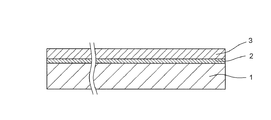
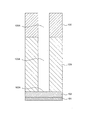
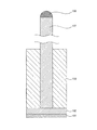
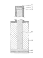
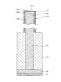
- FIG. 1 is a process diagram of a method for manufacturing a light-emitting element used in the light-emitting device according to the first embodiment of the present invention.
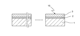
- FIG. 2 is a process diagram following FIG.
- FIG. 3 is a process diagram following FIG.
- FIG. 4 is a process diagram of a method for manufacturing a light-emitting element used in the light-emitting device according to the second embodiment of the present invention.
- FIG. 5 is a process diagram following FIG.
- FIG. 6 is a process diagram following FIG.
- FIG. 7 is a process diagram following FIG.
- FIG. 8 is a process diagram following FIG.
- FIG. 9 is a process diagram following FIG.
- FIG. 10 is a process diagram following FIG.
- FIG. 11 is a process diagram following FIG.
- FIG. 12 is a process diagram following FIG.
- FIG. 13 is a process diagram following FIG.
- FIG. 14 is a process diagram following FIG.
- FIG. 15 is a process diagram following FIG.
- FIG. 16 is a process diagram following FIG.
- FIG. 17 is a process diagram following FIG.
- FIG. 18 is a plan view of an insulating substrate used in the light emitting device according to the third embodiment of the present invention.
- FIG. 19 is a schematic sectional view taken along line XIX-XIX in FIG.
- FIG. 20 is a view for explaining the principle of arranging the rod-shaped structure light emitting elements.
- FIG. 21A is a diagram for explaining potentials applied to electrodes when the rod-shaped structure light emitting elements are arranged.
- FIG. 21A is a diagram for explaining potentials applied to electrodes when the rod-shaped structure light emitting elements are arranged.
- FIG. 21B is a diagram for explaining the potential applied to the electrodes when the rod-shaped structure light emitting elements are arranged.
- FIG. 22 is a plan view of an insulating substrate on which the rod-shaped structure light emitting elements are arranged.
- FIG. 23 is a process drawing of the method for manufacturing the light emitting device according to the fourth embodiment of the present invention.
- FIG. 24 is a process diagram following FIG.
- FIG. 25 is a process diagram following FIG.
- FIG. 26 is a process diagram of the method for manufacturing the light emitting device according to the fifth embodiment of the present invention.
- FIG. 27 is a process diagram following FIG.
- FIG. 28 is a process diagram following FIG.
- FIG. 29 is a process diagram following FIG.
- FIG. 30 is a process drawing following FIG.
- FIG. 31 is a process diagram following FIG.
- FIG. 32 is a plan view of a light-emitting device used in the illumination device according to the sixth embodiment of the present invention.
- FIG. 33 is a side view of the light emitting device.
- FIG. 34 is a side view of an LED bulb as an example of an illumination device using the light emitting device.
- FIG. 35 is a plan view of a backlight using the light emitting device according to the seventh embodiment of the present invention.
- FIG. 36 is a cross-sectional view of a conventional light emitting device.
- FIG. 37 is a schematic cross-sectional view for explaining the heat outflow of the conventional light emitting device.
- FIG. 38 is a schematic cross-sectional view for explaining the heat outflow of the light emitting device of the present invention.
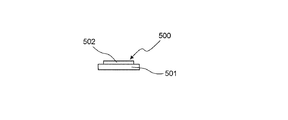
- FIG. 39 is a schematic cross-sectional view of a conventional light emitting device.
- FIG. 40 is a schematic cross-sectional view of the light emitting device of the present invention.
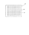
- FIG. 41 is a schematic plan view of the light emitting device of the present invention.
- FIG. 42 is a diagram showing a model used in the thermal simulation.
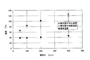
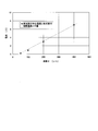
- FIG. 43 is a diagram showing the temperature of each part with respect to the diameter of the LED chip.
- FIG. 44 is a diagram showing the center temperature of the light emitting surface with respect to the diameter of the LED chip.
- FIG. 45 is a diagram showing a difference between the center temperature of the light emitting surface and the end temperature of the light emitting surface with respect to the diameter of the LED chip.
- FIG. 46A is a diagram illustrating a case where a light emitting surface of a light emitting element has a flat circular shape.
- FIG. 46B is a diagram illustrating a case where the light emitting surface of the light emitting element has a flat square shape.
- FIG. 46C is a diagram for explaining a case where a minute deformation is applied to a circle while keeping the area constant.
- a plurality of light-emitting elements each having a light-emitting surface area of 2500 ⁇ m 2 or less (more preferably 625 ⁇ m 2 or less) are arranged on the mounting surface of the same substrate.
- the plurality of light-emitting elements are not limited to light-emitting elements having a flat light-emitting surface such as a circular shape, an elliptical shape, a square shape, a rectangular shape, or a polygonal shape, but may have a cylindrical shape, a bowl shape, a hemispherical shape, or the like.
- a light emitting element having a light emitting surface formed of a curved surface may be used.
- FIG. 38 shows heat outflow when the diameter of the light emitting surface of the light emitting element 803 is less than 100 ⁇ m. As shown in FIG. 38, the heat in the lateral direction toward the substrate is also obtained at the center of the light emitting surface of the light emitting element 803. An outflow occurs.
- FIG. 42 shows a model used for the simulation.
- the heat conductive substrate 850 is assumed to be a general substrate on which LEDs are mounted.
- An aluminum substrate 851 having a thickness of 50 ⁇ m is covered with a resin coating 852 for insulation having a thickness of 50 ⁇ m.
- the thermally conductive substrate 850 was 10 cm in diameter.
- an LED chip 853 having a diameter ⁇ in which a light emitting layer made of GaN is formed on a sapphire substrate having a thickness of 10 ⁇ m is disposed.
- the total area (40000 ⁇ m 2 ) of the light emitting surface of the LED chip 853 disposed on the resin coating 852 is restricted so as to be always constant. That is, when the diameter ⁇ of the LED chip 853 was halved, the number of the LED chips 853 was increased four times and arranged substantially evenly on the resin coating 852. This is to make the amount of generated heat equal even if the diameter ⁇ of the LED chip 853 is changed.
- the thermally conductive substrate 850 is connected to the outside at room temperature (27 ° C.) with a thermal resistance Rth. This thermal resistance Rth reflects each thermal resistance from the resin substrate laid under the thermally conductive substrate 850, the metal installed in the heat radiation path, the heat radiation fin, and the heat radiation fin to the atmosphere.
- the thermal conductivity used in the thermal simulation is 237 W / mK for the aluminum substrate 851, 0.5 W / mK for the resin coating 852, and 35 W / mK for the sapphire substrate.
- the thermal resistance Rth was 75 ° C./W.
- the heat generation density of the light emitting surface was 10 6 W / m 2 .
- FIG. 43 is a graph showing the temperature of each part obtained by thermal simulation.
- “ ⁇ ” indicates the center temperature of the light emitting surface in a steady state (temperature at A in FIG. 42)
- ⁇ indicates the end temperature of the light emitting surface (temperature at B in FIG. 42)
- “ ⁇ ”. Is the substrate temperature (the temperature of the aluminum substrate 851 immediately below the LED chip 853 (the temperature at C in FIG. 42)) and shows the dependence of the LED chip 853 on the diameter ⁇ . Although not changed, this is because the total calorific value is constant.
- FIG. 44 is a graph displaying only the center temperature of the light emitting surface.
- the center temperature of the light emitting surface rapidly decreases (light emitting surface indicated by a dotted line in FIG. 44).
- the temperature drop is more remarkable than the tendency of the center temperature of This suggests that the heat flow in the lateral direction toward the substrate is also performed at the center of the light emitting surface, that is, the state shown in FIG. 38 is realized. Since the center temperature of the light emitting surface is the hottest part of the light emitting element, lowering this temperature improves the efficiency of the light emitting element and suppresses the deterioration of the surrounding resin and phosphor. It means that the life can be extended.
- FIG. 45 is a graph displaying the difference between the center temperature of the light emitting surface and the end temperature of the light emitting surface.
- the difference between the center temperature of the light surface and the end temperature of the light emitting surface is an index indicating how much heat is accumulated near the center of the light emitting surface.
- the temperature decrease is more remarkable than the tendency of the central temperature of the light emitting surface to decrease as indicated by the dotted line 44).
- the LED chip 853 has a diameter of 50 ⁇ m or less, no heat is accumulated in the vicinity of the center of the light emitting surface, and the lateral heat outflow to the substrate side is performed extremely efficiently. Therefore, the temperature rise at the time of light emission is remarkably suppressed, and further life extension and high efficiency of the light emitting device are realized.
- the light emitting surface of the light emitting element has a flat circular shape
- the light emitting element is flat and has an arbitrary shape.
- the light emitting surface of the light emitting element is a flat square shape
- the shortest distance from an arbitrary point on the light emitting surface of the light emitting element to the outer edge is less than 44.31 ⁇ m, and heat flows in the lateral direction toward the substrate also at the center of the light emitting surface.
- the shortest distance from an arbitrary point on the light emitting surface of the light emitting element to the outer edge is less than 44.31 ⁇ m, and heat flows in the lateral direction toward the substrate also at the center of the light emitting surface.
- the shortest distance from the center of the circle to the outer edge is shortened by any minute deformation while keeping the area constant with respect to the circle. That is, when the light emitting surface of the light emitting element has the same area, heat is most difficult to escape when it is a flat circular shape, and when the area of the light emitting surface is 2500 ⁇ m 2 or less, an elliptical shape, a square shape, a rectangular shape, In other flat light emitting surfaces such as a polygonal shape, the shortest distance from any point on the light emitting surface of the light emitting element to the outer edge is always less than 50 ⁇ m, and the lateral heat toward the substrate is also at the center of the light emitting surface. Since outflow is performed, the temperature rise at the time of light emission is suppressed.
- the light emitting elements are rod-shaped and the light emitting surface is cylindrical
- the light emitting elements are mounted on the board so that the longitudinal direction of the light emitting elements is parallel to the board mounting surface.
- the distance from any point on the light emitting surface of the light emitting element to the outer edge is much shorter than that of the flat light emitting surface, and at any point on the light emitting surface the lateral direction (axis of the axis) Since heat flows out on both sides), temperature rise during light emission is effectively suppressed.
- the brightness variation among the light emitting elements may reach 50% due to the variation of the forward voltage (Vf).
- Vf forward voltage
- the resin that covers the light emitting element deteriorates due to the light emitted from the light emitting element, resulting in a short life.
- the light emitting element is miniaturized and arranged on the mounting surface of the same substrate. By doing so, for example, a light amount equivalent to that of a single light emitting element can be obtained by a plurality of fine light emitting elements, while the light applied to the resin can be dispersed and the light intensity can be weakened, and deterioration of the resin can be suppressed. Long life can be achieved.
- the light emitting device of the present invention by distributing the light emission while suppressing the temperature rise during light emission, there is little variation in brightness, and a long life and high efficiency can be realized.
- n-type GaN doped with Si and p-type GaN doped with Mg are used, but the impurity doped into GaN is not limited to this.
- First Embodiment 1 to 3 show process drawings of a method for manufacturing a light emitting element used in the light emitting device according to the first embodiment of the present invention.
- a quantum well layer 2 made of p-type InGaN is formed by epitaxial growth on the n-type GaN substrate 1 shown in FIG. 1, and then a p-type GaN layer 3 is formed on the quantum well layer 2 by epitaxial growth. Is deposited.
- the n-type GaN substrate 1 on which the quantum well layer 2 and the p-type GaN layer 3 are formed is divided into a plurality of semiconductor chips 10 as an example of a light emitting element by dicing.
- the divided semiconductor chip 10 has a square shape with one side of 50 ⁇ m or less, a thickness of 10 ⁇ m, and a flat light emitting surface.
- the quantum well layer 2 may include a p-type AlGaN layer as an electron blocking layer between the InGaN layer and the p-type GaN layer.
- a multiple quantum well structure in which GaN barrier layers and InGaN quantum well layers are alternately stacked may be employed.
- 100 or more of the semiconductor chips 10 shown in FIG. 3 are distributed substantially evenly on the mounting surface of the same substrate.
- a plurality of semiconductor chips 10 each having an area of the light emitting surface of 2500 ⁇ m 2 or less (more preferably 625 ⁇ m 2 or less) are arranged on the mounting surface of the same substrate. Also in the central portion of the light source, lateral heat flow out to the substrate side is performed, and the temperature of the light emitting element including the central portion of the light emitting surface is lowered, so that the temperature rise during light emission is suppressed. Then, by arranging 100 or more such fine semiconductor chips 10 on the mounting surface of the same substrate, the variation in overall brightness when a plurality of semiconductor chips 10 having brightness variations are gathered is 1 It can be reduced to 1/10 or less of the brightness variation of the two semiconductor chips 10.
- the area of the light emitting surface per one semiconductor chip 10 is set to 2500 ⁇ m 2 or less (more preferably 625 ⁇ m 2 or less). Since the temperature rise is suppressed and the variation in the amount of decrease in the light emission efficiency is suppressed, the effect of reducing the brightness variation by using 100 or more fine semiconductor chips 10 is further enhanced.
- a light amount equivalent to that of one light emitting element can be obtained with a plurality of fine semiconductor chips 10 while irradiating the resin.
- the dispersed light can be dispersed and the light intensity can be weakened, and the life of the resin can be extended by suppressing the deterioration of the resin.
- the light emitting device by dispersing the light emission while suppressing the temperature rise during light emission, there is little variation in brightness, and a long life and high efficiency can be realized.
- the heat generated in the light emitting elements due to the light emission is arranged. Since the outflow in the lateral direction is efficiently performed, the temperature rise during light emission is further suppressed, and the lifetime can be further increased and the efficiency can be improved.
- a square light emitting element having a flat light emitting surface is used.
- the light emitting element of the present invention is not limited to this, and a flat light emitting surface having a circular shape, an elliptical shape, a rectangular shape, a polygonal shape, or the like. The light emitting element which has this may be sufficient.
- FIGS. 4 to 17 are process diagrams sequentially showing a method for manufacturing a light emitting device according to the second embodiment of the present invention.
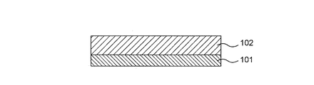
- the prepared sapphire substrate 101 is cleaned.
- an n-type GaN film 102 is formed on the sapphire substrate 101.
- a mask layer 103 is formed on the n-type GaN film 102 by deposition.
- the mask layer 103 is made of, for example, SiN or SiO 2 .
- a resist layer 105 is applied onto the mask layer 103, exposed and developed (development), and further dry-etched to form holes 105A in the resist layer 105 and the mask layer 103 as shown in FIG. , 103A.
- a part 102A of the n-type GaN film 102 is exposed through the holes 105A and 103A.
- the mask layer 103 serves as a growth mask, and a hole 103A formed in the mask layer 103 serves as a growth hole.
- a catalyst metal 106 is deposited (deposited) on the resist layer 105 and on a portion 102A of the n-type GaN film 102 exposed in the hole 103A.
- this catalytic metal 106 for example, Ni, Fe or the like can be adopted.
- the resist layer 105 and the catalyst metal 106 on the resist layer 105 are removed by lift-off, leaving the catalyst metal 106 on a part 102A of the n-type GaN film 102 as shown in FIG. I do.
- n-type GaN is crystal-grown using an MOCVD (Metal Organic Chemical Vapor Deposition) apparatus in the presence of the catalytic metal 106.
- MOCVD Metal Organic Chemical Vapor Deposition
- a rod-shaped semiconductor core 107 having a substantially hexagonal cross section is formed.
- the rod-shaped semiconductor core 107 is grown to a length of 25 ⁇ m, for example.
- the growth temperature is set to about 800 ° C.
- trimethylgallium (TMG) and ammonia (NH 3 ) are used as growth gases
- silane (SiH 4 ) is used for supplying n-type impurities
- hydrogen (H 2 ) is used as a carrier gas.
- the n-type semiconductor core 107 with Si as an impurity can be grown.
- the n-type GaN has hexagonal crystal growth, and a hexagonal column-shaped semiconductor core is obtained by growing the n-type GaN with the c-axis direction perpendicular to the surface of the sapphire substrate 101.
- the cross section tends to be almost circular, and the diameter is 0.5 ⁇ m.
- the thickness is increased from about a few ⁇ m, it tends to be easy to grow the cross section in a substantially hexagonal shape.
- a plurality of holes 105A in the resist layer 105 and a plurality of holes 103A in the mask layer 103 are formed, and a catalytic metal 106 is formed in a part 102A of the n-type GaN film 102 at a plurality of positions exposed in the plurality of holes 105A and 103A.
- a plurality of rod-shaped semiconductor cores 107 are formed.
- a quantum well layer 108 made of p-type InGaN is formed by MOCVD so as to cover the semiconductor core 107 made of n-type GaN and the mask layer 103.
- the quantum well layer 108 has a set temperature of 750 ° C. according to the emission wavelength, supplies nitrogen (N 2 ) as a carrier gas, TMG, NH 3 , and trimethylindium (TMI) as a growth gas, so that an n-type GaN A quantum well layer 108 made of p-type InGaN can be formed on the semiconductor core 107 and the mask layer 103.
- a p-type AlGaN layer may be inserted as an electron blocking layer between the InGaN layer and the p-type GaN layer.
- a multiple quantum well structure in which GaN barrier layers and InGaN quantum well layers are alternately stacked may be employed.
- a semiconductor layer 110 made of p-type GaN is formed on the entire surface of the quantum well layer 108 by MOCVD.
- the semiconductor layer 110 can be formed of p-type GaN by setting the set temperature to 900 ° C., using TMG and NH 3 as growth gases, and using Cp 2 Mg for supplying p-type impurities.
- the catalyst metal 106 and the semiconductor core are compared with the growth rate of the portion covering the side surface 107B of the semiconductor core 107.
- the growth rate of the portion between the front end surface 107A of 107 is fast, for example, 10 to 100 times.
- the growth rate of GaN at the location where the catalytic metal 106 is adhered is 50 to 100 ⁇ m / hour
- the growth rate of GaN at the location where the catalytic metal is not adhered is 1 to 2 ⁇ m / hour. . Therefore, in the quantum well layer 108 and the semiconductor layer 110, the film thicknesses of the front end portions 108A and 110A are larger than the film thicknesses of the side surface portions 108B and 110B.
- the catalyst metal 106 on the semiconductor core 107 is removed by etching and then washed, and the semiconductor layer 110 is activated by annealing.
- the quantum well layer 108 covering the front end surface 107A of the semiconductor core 107 and the thickness of the front end portions 108A and 110A of the semiconductor layer 110 are the quantum well layer 108 covering the side surface 107B of the semiconductor core 107 and the side surface portion of the semiconductor layer 110. Since it is thicker than the thickness of 108B and 110B, damage and defects on the metal removal surface are less likely to adversely affect the PN junction.
- the semiconductor core 107 can be prevented from being exposed from the semiconductor layer 110 during etching.
- a conductive film 111 is formed on the entire surface of the semiconductor layer 110 made of p-type GaN.
- Polysilicon, ITO (tin-added indium oxide), or the like can be used as the material of the conductive film 111.
- the film thickness of the conductive film 111 is, for example, 200 nm.
- the contact resistance between the semiconductor layer 110 made of p-type GaN and the conductive film 111 can be reduced by performing heat treatment at 500 ° C. to 600 ° C.
- the conductive film 111 is not limited to this, and for example, a 5 nm thick Ag / Ni or Au / Ni semi-transparent laminated metal film may be used.
- Vapor deposition or sputtering can be used to form this laminated metal film. Further, in order to further reduce the resistance of the conductive layer, a laminated metal film of Ag / Ni or Au / Ni may be laminated on the conductive film made of ITO.
- a portion of the conductive film 111 extending in the lateral direction on the semiconductor core 107 and the mask layer 103 is removed by dry etching RIE (reactive ion etching). Further, the tip portion 110A of the semiconductor layer 110 covering the tip surface 107A of the semiconductor core 107 is removed by a certain thickness by the RIE. Further, the semiconductor layer 110 in a region extending in the lateral direction beyond the conductive film 111 on the mask layer 103 is removed by the RIE. In addition, the quantum well layer 108 in the region extending laterally beyond the conductive film 111 on the mask layer 103 is removed by the RIE.
- RIE reactive ion etching
- the film thickness of the front end portion 108A of the quantum well layer 108 is sufficiently thicker than the film thickness of the side surface portion 108B, and the film thickness of the front end portion 110A of the semiconductor layer 110 is increased. Since it is sufficiently thicker than the film thickness of 110B, the semiconductor core 107 is not exposed at the tip after the RIE. Therefore, the quantum well layer 108 and the semiconductor layer 110 that cover the front end surface of the semiconductor core 107 and the quantum well layer 108, the semiconductor layer 110, and the conductive film 111 that cover the side surface of the semiconductor core 107 remain by the RIE.
- the mask layer 103 (shown in FIG. 14) is removed by etching.
- the semiconductor core 107 and the semiconductor core 107 can be easily formed by using a solution containing hydrofluoric acid (HF).
- the mask layer 103 can be etched without affecting the portions of the semiconductor layer 110 and the conductive film 111 that cover the surface.
- by dry etching using CF 4 or XeF 2 the mask layer 103 can be easily etched without affecting the semiconductor core 107, the semiconductor layer 110 covering the semiconductor core 107, and the conductive film 111.
- the semiconductor core 107 exposes the outer peripheral surface of the exposed portion 107C on the sapphire substrate 101 side.
- the underlying n-type GaN film 102 is etched by RIE (reactive ion etching) to expose the surface of the sapphire substrate 101.
- RIE reactive ion etching
- a step portion 102B made of n-type GaN connected to the semiconductor core 107 is formed.
- the RIE makes it possible to The tip surface 107A can be prevented from being exposed.
- a rod-like structure including the semiconductor core 107 made of n-type GaN, the quantum well layer 108 made of p-type InGaN, the semiconductor layer 110 made of p-type GaN, the conductive film 111, and the step portion 102B made of n-type GaN.
- the light emitting element is formed on the sapphire substrate 101.
- the substrate is immersed in an isopropyl alcohol (IPA) aqueous solution, and the base substrate (sapphire substrate 101) is vibrated along the plane of the substrate using ultrasonic waves (for example, several tens of kHz).
- IPA isopropyl alcohol
- the quantum well layer 108, the semiconductor layer 110, and the semiconductor core 107 covered with the conductive film 111 are stressed so that the semiconductor core 107 standing upright is bent.
- the semiconductor core 110 covered with the semiconductor layer 110 and the conductive film 111 is separated from the base substrate.
- a fine rod-shaped light emitting element separated from the base substrate can be manufactured.
- the semiconductor core 107 is separated from the substrate using ultrasonic waves, the present invention is not limited thereto, and the semiconductor core 107 may be separated by mechanically bending the semiconductor core from the substrate using a cutting tool. In this case, a plurality of fine rod-shaped light emitting elements provided on the substrate can be separated in a short time by a simple method.
- the semiconductor layer 110 grows in the radial direction outward from the outer peripheral surface of the semiconductor core 107, the radial growth distance is short, and the defects escape outward, so the semiconductor layer 110 with few crystal defects.
- the semiconductor core 107 can be covered. Therefore, it is possible to realize a rod-shaped structure light emitting device with good characteristics.
- the rod-shaped structure light emitting element 100 can reduce the amount of semiconductor to be used, can reduce the thickness and weight of the device using the light emitting element, and can also reduce the entire circumference of the semiconductor core 107 covered with the semiconductor layer 110. Since the light emitting region is widened by emitting light from the light emitting device, a light emitting device, a backlight, a lighting device, a display device, and the like with high luminous efficiency and power saving can be realized. Further, as shown in FIG.
- the base n-type GaN film 102 is etched by RIE (reactive ion etching) to form the stepped portion 102B. However, the etching of the base n-type GaN film 102 is omitted.
- the semiconductor core 107 may be separated from the base n-type GaN film 102 without the portion 102B to produce a rod-shaped structure light emitting element that does not have the stepped portion 102B.
- the rod-shaped structure light emitting device 100 has a diameter of 1 ⁇ m and a length of 25 ⁇ m, the light emission area of each rod-shaped structure light emitting device 100, that is, the area of the quantum well layer 108 is approximately (25 ⁇ ⁇ ⁇ (0 5) 2 ⁇ m 2 ⁇ (peripheral area of the exposed portion 107C)) (2,500 ⁇ m 2 or less).
- the rod-shaped structure light emitting elements 100 are the same so that the longitudinal direction of the rod-shaped structure light emitting elements 100 shown in FIG. 17 is parallel to the mounting surface of the substrate (not shown). More than 100 pieces are distributed on the mounting surface of the substrate substantially evenly.
- the light emitting device by arranging a plurality of rod-shaped structure light emitting elements 100 having a light emitting surface area of 2500 ⁇ m 2 or less (more preferably 625 ⁇ m 2 or less) on the mounting surface of the same substrate, Even in the central portion of the light emitting surface, heat is discharged in the lateral direction to the substrate side, and the temperature of the light emitting element including the central portion of the light emitting surface is lowered, so that an increase in temperature during light emission is suppressed. And by arranging 100 or more such fine rod-shaped structure light emitting elements 100 on the mounting surface of the same substrate, the overall brightness when a plurality of rod-shaped structure light emitting elements 100 having brightness variations are gathered is collected.
- the variation can be reduced to 1/10 or less of the brightness variation of one bar-shaped light emitting element 100.
- Decrease in luminous efficiency due to temperature rise of the rodlike structure light emitting element 100 varies for each device, but the area of the light emitting surface per one of the rod-like structure light-emitting element 100 2,500Paimyuemu 2 or less (more preferably 625Paimyuemu 2 below) Therefore, the temperature rise is suppressed and the variation in the amount of decrease in the light emission efficiency is suppressed, so that the effect of reducing the brightness variation by using 100 or more fine rod-shaped light emitting elements 100 is further enhanced.
- a plurality of the fine rod-shaped structure light emitting devices 100 can obtain the same amount of light as one light emitting device.
- the light applied to the resin is dispersed and the light intensity can be weakened, and the life of the resin can be extended by suppressing the deterioration of the resin.
- the light emitting device by dispersing the light emission while suppressing the temperature rise during light emission, there is little variation in brightness, and a long life and high efficiency can be realized.
- the plurality of rod-shaped structure light emitting elements 100 are arranged substantially uniformly distributed on a substrate (not shown) having an area of four times or more the total light emitting area of the plurality of rod-shaped structure light emitting elements 100. Since the heat generated in the rod-like structure light emitting element 100 due to light emission is efficiently discharged in the lateral direction to the substrate side, the temperature rise during light emission is further suppressed, and the life and efficiency can be further increased.
- the plurality of rod-shaped structure light emitting elements 100 are arranged on the mounting surface of the substrate so that the longitudinal direction of the plurality of rod-shaped structure light emitting elements 100 is parallel to the mounting surface of the substrate (not shown), Since the ratio of the length in the axial direction (longitudinal direction) to the radial direction can be increased, heat flow in the lateral direction toward the substrate side is more efficient than when the light emitting surface is square under the same light emitting surface area. As a result, the temperature rise at the time of light emission is further suppressed, and a longer life and higher efficiency can be achieved.
- the rod-shaped rod-shaped structure light emitting device 100 has a cylindrical light-emitting surface (quantum well layer 108) concentrically surrounding the rod-shaped semiconductor core 107, so that the area of the light-emitting surface per one is 2500 ⁇ m 2.
- Light emission per one rod-shaped structure light-emitting element 100 within the condition that a plurality of rod-shaped structure light-emitting elements 100 of the following (more preferably 625 ⁇ m 2 or less) are arranged on the mounting surface of the same substrate. The area of the surface increases, the number of light emitting elements for obtaining a predetermined brightness can be reduced, and the cost can be reduced.
- the rod-shaped rod-shaped structure light emitting element 100 includes a p-type rod-shaped semiconductor core 107 and an n-type cylindrical semiconductor layer 110 formed so as to cover the outer periphery of the semiconductor core 107. Since one end side of 107 is exposed, it is possible to connect one electrode to the exposed portion 107C on one end side of the semiconductor core 107 and connect the electrode to the semiconductor layer 110 on the other end side of the semiconductor core 107, Since the electrodes can be connected to both ends separately, and the electrode connected to the semiconductor layer 110 and the exposed portion 107C of the semiconductor core 107 are prevented from being short-circuited, wiring can be facilitated.
- the cross sections of the exposed portion 107C of the semiconductor core 107 and the covering portion covered with the semiconductor layer 110 are not limited to hexagonal shapes, and may be other polygonal or circular cross sectional shapes.
- the exposed portion and the covering portion may have different cross-sectional shapes.
- the p-type semiconductor layer 110 is formed not only on the tip surface 107A of the n-type semiconductor core 107 but also on the side surface 107B, so that the area of the pn junction is increased.
- the light emission area can be increased and the light emission efficiency can be improved.
- the n-type semiconductor core 107 is formed using the catalyst metal 106, the growth rate of the n-type semiconductor core 107 can be increased. For this reason, the semiconductor core 107 can be lengthened in a short time compared to the conventional case, and the light emitting area that is proportional to the length of the n-type semiconductor core 107 can be further increased.
- the electrode for the p-type semiconductor layer 110 and the n-type semiconductor core 107 are short-circuited. Can be prevented.
- the p-type quantum well layer 108 and the p-type semiconductor layer 110 are formed with the catalyst metal 106 left, so that the n-type semiconductor core 107 is formed. And the p-type quantum well layer 108 and the p-type semiconductor layer 110 can be continuously formed in the same manufacturing apparatus. Therefore, process reduction and manufacturing time can be shortened. Further, since it is not necessary to take the semiconductor core 107 out of the manufacturing apparatus after forming the n-type semiconductor core 107, contamination can be prevented from adhering to the surface of the n-type semiconductor core 107, and the device characteristics can be improved. .
- the formation of the n-type semiconductor core 107 and the formation of the p-type quantum well layer 108 and the p-type semiconductor layer 110 can be performed continuously, it is possible to avoid a large temperature change or stop of growth. Thus, crystallinity can be improved and device characteristics can be improved. Further, by not performing etching to remove the catalytic metal 106 immediately after forming the n-type semiconductor core 107, the surface of the n-type semiconductor core 107 (that is, the interface with the p-type semiconductor layer 110) is removed. Damage can be eliminated and device characteristics can be improved.
- the growth rate of the portion in contact with the catalytic metal 106 is the catalytic metal. Compared to the growth rate of the portion not in contact with 106, the growth rate is significantly faster (for example, 10 to 100 times). Therefore, a light-emitting element with a high dimension aspect ratio can be manufactured.
- the rod-shaped structure light emitting element 100 has a diameter of 1 ⁇ m and a length of 25 ⁇ m.
- the n-type semiconductor core 107 and the p-type semiconductor layer 110 can be successively stacked under the catalyst metal 106, defects at the PN junction can be reduced.
- the mask layer 103 is removed and the exposed portion 107C of the semiconductor core 107 on the sapphire substrate 101 side is exposed, so that the etching amount of the semiconductor layer 110 can be reduced.
- the rod-shaped structure light emitting element 100 can be easily contacted with the semiconductor core 107 by the step portion 102 ⁇ / b> B made of n-type GaN connected to the semiconductor core 107. Further, the rod-shaped structure light emitting device 100 can improve the light emission efficiency by the quantum well layer 108.
- the n-type GaN film 102 is formed on the sapphire substrate 101.
- the step of forming the n-type GaN film 102 on the sapphire substrate 101 is eliminated, and the mask is directly formed on the sapphire substrate 101.
- the layer 103 may be formed.
- the catalyst metal 106 on the semiconductor core 107 is removed by etching in the catalyst metal removal step.
- the catalyst metal removal step is eliminated, and the conductive film 111 is formed with the catalyst metal 106 left. May be.
- the conductive film 111, the semiconductor layer 110 made of p-type GaN, and the quantum well layer 108 are etched by RIE. However, this etching process by RIE is eliminated, and the next mask is formed.
- the mask layer 103 may be removed by simultaneous lift-off of each layer.
- the semiconductor core 107 is crystal-grown using the MOCVD apparatus.
- the semiconductor core may be formed using another crystal growth apparatus such as an MBE (molecular beam epitaxial) apparatus.
- MBE molecular beam epitaxial
- the semiconductor core may be crystal-grown from the metal species by arranging a metal species on the substrate.
- the semiconductor core 107 covered with the semiconductor layer 110 is separated from the sapphire substrate 101 using ultrasonic waves.
- the present invention is not limited to this, and the semiconductor core is mechanically removed from the substrate using a cutting tool. May be bent and separated. In this case, a plurality of fine rod-shaped light emitting elements provided on the substrate can be separated in a short time by a simple method.
- FIG. 18 is a plan view of an insulating substrate used in the method for manufacturing a light emitting device according to the third embodiment of the present invention.
- the rod-shaped structure light-emitting element used in the light-emitting device of the third embodiment may use the light-emitting elements of the first and second embodiments, or other rod-shaped light-emitting elements.
- an insulating substrate in which metal electrodes 201 and 202 as an example of the first and second electrodes are formed on the mounting surface in the substrate creation step. 200 is created.
- the insulating substrate 200 is an insulator such as glass, ceramic, aluminum oxide, resin, or a substrate in which a silicon oxide film is formed on a semiconductor surface such as silicon, and the surface is insulative.
- a base insulating film such as a silicon oxide film or a silicon nitride film on the surface.
- the metal electrodes 201 and 202 are formed in a desired electrode shape using a printing technique.
- the metal film and the photosensitive film may be uniformly laminated, and a desired electrode pattern may be exposed and etched.
- pads are formed on the metal electrodes 201 and 202 so that a potential can be applied from the outside.
- the rod-shaped structure light emitting elements are arranged in a portion (array region) where the metal electrodes 201 and 202 face each other.
- the array region in which the rod-shaped structure light emitting elements are arrayed is 9 ⁇ 3.
- an arbitrary number of array regions of 100 or more is used.
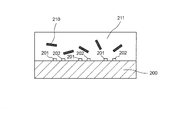
- FIG. 19 is a schematic sectional view taken along line XIX-XIX in FIG.
- isopropyl alcohol (IPA) 211 including a rod-shaped structure light emitting element 210 is thinly coated on the insulating substrate 200.
- IPA isopropyl alcohol
- ethylene glycol, propylene glycol, methanol, ethanol, acetone, or a mixture thereof may be used.
- the IPA 211 can use a liquid made of another organic material, water, or the like.
- an insulating film of about 10 nm to 30 nm may be coated on the entire surface of the insulating substrate 200 so as to cover the metal electrodes 201 and 202.
- the thickness of the application of the IPA 211 including the rod-shaped structure light emitting element 210 is such that the rod-shaped structure light emitting element 210 can move in the liquid so that the rod-shaped structure light emitting element 210 can be arranged in the next step of arranging the rod-shaped structure light emitting element 210. That's it. Therefore, the thickness of applying the IPA 211 is equal to or greater than the thickness of the rod-shaped structure light emitting element 210, and is, for example, several ⁇ m to several mm. If the applied thickness is too thin, the rod-like structure light emitting element 210 is difficult to move. If it is too thick, the time for drying the liquid becomes long. Further, the amount of the rod-like structure light emitting element 210 is preferably 1 ⁇ 10 4 pieces / cm 3 to 1 ⁇ 10 7 pieces / cm 3 with respect to the amount of IPA.
- a frame is formed on the outer periphery of the metal electrode on which the rod-shaped structure light emitting element 210 is arranged, and the IPA 211 including the rod-shaped structure light emitting element 210 is formed in a desired thickness. It may be filled so that However, when the IPA 211 including the rod-shaped structure light emitting element 210 has viscosity, it can be applied to a desired thickness without the need for a frame.
- a liquid made of IPA, ethylene glycol, propylene glycol,..., Or a mixture thereof, or other organic substances, or a liquid such as water is desirable as the viscosity is low for the alignment process of the rod-shaped structure light emitting device 210. It is desirable that it evaporates easily when heated.
- a potential difference is applied between the metal electrodes 201 and 202.
- the potential difference between the metal electrodes 201 and 202 can be 0.1 to 10 V.
- the voltage difference is 0.1 V or less, the arrangement of the rod-like structure light emitting elements 210 is poor, and if it is 10 V or more, insulation between the metal electrodes becomes a problem. start. Therefore, it is preferably 1 to 5V, more preferably about 1V.
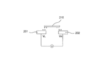
- FIG. 20 shows the principle that the rod-shaped structure light emitting elements 210 are arranged on the metal electrodes 201 and 202.
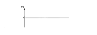
- a potential VL is applied to the metal electrode 201 and a potential VR (VL ⁇ VR) is applied to the metal electrode 202
- a negative charge is induced in the metal electrode 201 and a positive charge is applied to the metal electrode 202.
- VL ⁇ VR potential VR
- the rod-shaped structure light emitting element 210 approaches there, a positive charge is induced on the side close to the metal electrode 201 and a negative charge is induced on the side close to the metal electrode 202 in the rod-shaped structure light emitting element 210.
- the charge is induced in the rod-like structure light emitting element 210 due to electrostatic induction.
- the rod-shaped structure light emitting element 210 placed in the electric field is caused by the charge being induced on the surface until the internal electric field becomes zero.
- an attractive force is exerted between each electrode and the rod-shaped structure light emitting element 210 by an electrostatic force, and the rod-shaped structure light emitting element 210 follows the lines of electric force generated between the metal electrodes 201 and 202 and also has each rod-shaped structure light emitting element 210.
- the repulsive force caused by the charges causes the charges to be regularly arranged in a fixed direction at almost equal intervals.
- the orientation of the exposed portion side of the semiconductor core 107 covered with the semiconductor layer 110 is not constant and is random.
- the rod-like structure light emitting element 210 generates charges in the rod-like structure light emitting element 210 by the external electric field generated between the metal electrodes 201 and 202, and the rod-like structure light emitting element 210 is applied to the metal electrodes 201 and 202 by the attractive force of the charges. Therefore, the size of the rod-shaped structure light emitting element 210 needs to be a size that can move in the liquid. Therefore, the size of the rod-shaped structure light emitting element 210 varies depending on the application amount (thickness) of the liquid. When the liquid application amount is small, the rod-like structure light emitting element 210 must be nano-order size, but when the liquid application amount is large, it may be micro order size.
- the rod-shaped structure light emitting device 210 When the rod-shaped structure light emitting device 210 is not electrically neutral and is charged positively or negatively, the rod-shaped structure light emitting device 210 is simply formed by applying a static potential difference (DC) between the metal electrodes 201 and 202. It cannot be arranged stably. For example, when the rod-shaped structure light emitting element 210 is positively charged as a net, the attractive force with the metal electrode 202 in which the positive charge is induced becomes relatively weak. Therefore, the arrangement of the rod-shaped structure light emitting elements 210 is untargeted.
- DC static potential difference
- the frequency of the AC voltage applied to the metal electrode 202 is preferably 10 Hz to 1 MHz, and more preferably 50 Hz to 1 kHz because the arrangement is most stable.
- the AC voltage applied between the metal electrodes 201 and 202 is not limited to a sine wave, but may be any voltage that varies periodically, such as a rectangular wave, a triangular wave, and a sawtooth wave.
- VPPL was preferably about 1V.
- the insulating substrate 200 is heated to evaporate and dry the liquid. They are arranged at equal intervals along the lines of electric force between 202 and fixed.
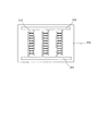
- FIG. 22 is a plan view of the insulating substrate 200 on which the rod-shaped structure light emitting elements 210 are arranged.
- the number of bar-shaped light emitting elements 210 is reduced to make the drawing easier to see, but actually, 100 or more bar-shaped light emitting elements 210 are arranged on the same insulating substrate 200.
- the insulating substrate 200 on which the rod-shaped structure light emitting elements 210 shown in FIG. 22 are arranged is used for a backlight of a liquid crystal display device, etc., thereby realizing a backlight that can be reduced in thickness and weight, has a high luminous efficiency, and saves power. can do. Further, by using the insulating substrate 200 on which the rod-shaped structure light emitting elements 210 are arranged as a lighting device, it is possible to realize a lighting device that can be reduced in thickness and weight, has high luminous efficiency, and saves power.
- the polarities of pn of the rod-shaped structure light emitting elements 210 are not aligned on one side but are randomly arranged. For this reason, at the time of driving, it is driven by an alternating voltage, and the bar-shaped structure light emitting elements 210 having different polarities emit light alternately.
- an insulating substrate 200 having an array region having two metal electrodes 201 and 202 each having an independent potential applied thereto is formed, and the insulating substrate 200 is formed on the insulating substrate 200.
- a liquid containing a plurality of rod-shaped light emitting elements 210 having a light emission area of 2500 ⁇ m 2 or less (more preferably 625 ⁇ m 2 or less) is applied. Thereafter, independent voltages are applied to the two metal electrodes 201 and 202, respectively, so that the fine rod-shaped light emitting elements 210 are arranged at positions defined by the two metal electrodes 201 and 202. Thereby, the rod-shaped structure light emitting element 210 can be easily arranged on the predetermined insulating substrate 200.
- the amount of semiconductor used can be reduced.
- the light emitting element 210 has a light emitting area that is widened by emitting light from the entire side surface of the semiconductor core covered with the semiconductor layer, and thus a light emitting device with high luminous efficiency and low power consumption can be realized. it can.
- the plurality of light emitting elements are substantially uniformly distributed on the mounting surface of the insulating substrate 200 having an area of four times or more the total light emitting area of the plurality of rod-shaped structure light emitting elements 210.
- heat generated in the light emitting element due to light emission is efficiently discharged in the lateral direction, so that a temperature increase during light emission is further suppressed, and a longer life and higher efficiency can be achieved.
- the rod-shaped structure light emitting elements 210 are arranged on the mounting surface of the insulating substrate 200 so that the longitudinal direction of the plurality of rod-shaped structure light emitting elements 210 is parallel to the mounting surface of the insulating substrate 200, the diameter Since the ratio of the length in the axial direction (longitudinal direction) to the direction can be increased, the heat flow in the lateral direction to the insulating substrate 200 is more efficient than when the light emitting surface is square under the same light emitting surface area. As a result, the temperature rise at the time of light emission is further suppressed, and a longer life and higher efficiency can be achieved. In addition, since this method of manufacturing a light-emitting device uses polarization of an object by applying a voltage between electrodes, it is convenient for polarizing both ends of a rod-shaped structure light-emitting element. Good compatibility.
- the rod-shaped structure light emitting element 210 is a light emitting diode having an anode connected to the metal electrode 201 (first electrode) and a cathode connected to the metal electrode 202 (second electrode); A light emitting diode having a cathode connected to the metal electrode 201 (first electrode) and an anode connected to the metal electrode 202 (second electrode) is mixed and disposed on the insulating substrate 200. .
- a plurality of light emitting diodes are driven by applying an AC voltage between the metal electrode 201 (first electrode) and the metal electrode 202 (second electrode) by an AC power source. It is not necessary to arrange the anode and the cathode in the same direction with respect to the light emitting diode, and the process can be simplified.
- the wiring process is simplified and the cost is reduced. Can be reduced.
- the rod-shaped structure light emitting element is used.
- the light emitting element is not limited to this, and a flat light emitting surface such as a circular shape, an elliptical shape, a square shape, a rectangular shape, or a polygonal shape is used.
- the light emitting element may be arranged on the mounting surface so that the light emitting surface thereof is parallel to the substrate.
- the manufacturing method of the light emitting device according to the third embodiment uses polarization of an object by applying a voltage between the electrodes, a rod-like light emitting element that is convenient for polarization is desirable.
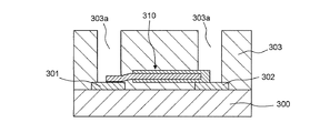
- [Fourth Embodiment] 23 to 25 show process drawings of a method for manufacturing a light emitting device according to the fourth embodiment of the present invention.
- a rod-shaped structure light-emitting element used in this method for manufacturing a light-emitting device has a first-conductivity-type rod-shaped semiconductor core and a second-conductivity-type cylindrical semiconductor layer formed so as to cover the outer periphery of the semiconductor core. And what is necessary is just the one end side of the semiconductor core of a rod-shaped light emitting element exposed.
- a conductive substrate 300 is formed.
- the rod-shaped structure light emitting elements 310 are arranged on the insulating substrate 300 so that the longitudinal direction is parallel to the mounting surface of the insulating substrate 300.
- the rod-shaped structure light emitting elements 310 in the liquid are arranged on the metal electrodes 301 and 302 using the same method as the method for manufacturing the light emitting device of the third embodiment, and then the insulating substrate 300 is formed.
- the liquid is evaporated and dried, and the rod-shaped structure light emitting elements 310 are arranged at equal intervals along the lines of electric force between the metal electrodes 301 and 302 and fixed.
- the bar-shaped structured light emitting element 310 includes a semiconductor core 311 made of a rod-shaped n-type GaN and an exposed portion 311a other than the exposed portion 311a of the semiconductor core 311 so as not to cover a portion on one end side of the semiconductor core 311. And a semiconductor layer 312 made of p-type GaN covering the covering portion 311b.
- the exposed portion 311 a on one end side of the rod-shaped structure light emitting element 310 is connected to the metal electrode 301, and the semiconductor layer 312 on the other end side of the rod-shaped structure light emitting element 310 is connected to the metal electrode 302.
- an interlayer insulating film 303 is formed on the insulating substrate 300, and the interlayer insulating film 303 is patterned to form contact holes 303a on the metal electrode 301 and the metal electrode 302, respectively. To do.
- metal wirings 304 and 305 are formed so as to fill the two contact holes 303a.
- the light emitting area per rod-shaped structure light emitting element 310 is set to 2500 ⁇ m 2 or less (more preferably 625 ⁇ m 2 or less). 23 to 25, the central portion of the rod-shaped structure light emitting element 310 is shown in a state of being lifted from the insulating substrate 300, but actually, the rod-shaped structure light emitting element 310 is the rod-shaped structure light emitting device of the third embodiment.
- the central portion When drying the IPA aqueous solution in the element arrangement method, the central portion is bent on the insulating substrate 300 due to stiction generated when droplets in the gap between the surface of the insulating substrate 300 and the rod-shaped structure light emitting element 310 are reduced by evaporation. It touches. Even when the rod-shaped light emitting element 310 is not in direct contact with the insulating substrate 300, the rod-shaped light emitting element 310 is in contact with the insulating substrate 300 through the interlayer insulating film 303.
- a metal part is provided between the central part of the rod-shaped structure light emitting element 310 and the insulating substrate 300 so as to support the rod-shaped structure light emitting element 310, and the central part of the rod-shaped structure light emitting element 310 is interposed via the metal part. It may be in contact with the insulating substrate 300.
- a light emitting device According to the above method for manufacturing a light emitting device, it is not necessary to dispose light emitting diodes at predetermined positions on a substrate as in the prior art, and a large number of fine light emitting diodes are accurately disposed at predetermined positions. In addition, by dispersing light emission while suppressing a temperature rise during light emission, a light-emitting device that has little variation in brightness and can have a long lifetime and high efficiency can be manufactured.
- the plurality of rod-shaped structure light emitting elements 310 are substantially uniformly distributed on the mounting surface of the insulating substrate 300 having an area of four times or more the total light emitting area of the plurality of rod-shaped structure light emitting elements 310. By doing so, heat generated in the light emitting element due to light emission is efficiently discharged in the lateral direction to the substrate side, so that a temperature rise during light emission is further suppressed, and a longer life and higher efficiency can be achieved.
- the rod-shaped structure light emitting elements 310 are arranged on the mounting surface of the insulating substrate 300 so that the longitudinal direction of the plurality of rod-shaped structure light emitting elements 310 is parallel to the mounting surface of the insulating substrate 300, the diameter Since the ratio of the length in the axial direction (longitudinal direction) with respect to the direction can be increased, heat flow in the lateral direction toward the insulating substrate 300 is more efficient than when the light emitting surface is square under the same light emitting surface area. It is often performed, and the temperature rise at the time of light emission is further suppressed, and a longer life and higher efficiency can be achieved. In addition, since this method of manufacturing a light-emitting device uses polarization of an object by applying a voltage between electrodes, it is convenient for polarizing both ends of a rod-shaped structure light-emitting element. Good compatibility.
- the plurality of rod-shaped structure light emitting elements 310 are light emitting diodes having an exposed portion 311a as an anode and a covering portion 311b as a cathode, and the metal electrode 301 (first electrode) is an anode and the metal electrode 302 (first electrode). 2) and a light-emitting diode having a cathode connected to the metal electrode 301 (first electrode) and an anode connected to the metal electrode 302 (second electrode). Thus, it is disposed on the insulating substrate 300.
- a plurality of light emitting diodes are driven by applying an AC voltage between the metal electrode 301 (first electrode) and the metal electrode 302 (second electrode) by an AC power source. It is not necessary to arrange the anode and the cathode in the same direction with respect to the light emitting diode, and the process can be simplified.
- the rod-shaped structure light emitting element 310 has a cylindrical light emitting surface that concentrically surrounds the rod-shaped semiconductor core 311, the area of the light emitting surface per piece is 2500 ⁇ m 2 or less (more preferably 625 ⁇ m 2 or less).
- the area of the light emitting surface per rod-shaped structure light emitting element 310 is increased within a range where 100 or more of the plurality of rod-shaped structure light emitting elements 310 are arranged on the mounting surface of the same insulating substrate 300.
- the number of light emitting elements for obtaining a predetermined brightness can be reduced, and the cost can be reduced.
- the rod-shaped structure light emitting element 310 has a p-type rod-shaped semiconductor core 311 and an n-type cylindrical semiconductor layer 312 formed so as to cover the outer periphery of the semiconductor core 311. Since one end side is exposed, one electrode can be connected to the exposed portion 311a on one end side of the semiconductor core 311 and the electrode can be connected to the semiconductor layer 312 on the other end side of the semiconductor core 107. Since the electrodes can be separated from each other and the electrode connected to the semiconductor layer 312 and the exposed portion 311a of the semiconductor core 311 are prevented from being short-circuited, wiring can be facilitated.
- FIG. 31 are process diagrams of the method for manufacturing the light emitting device according to the fifth embodiment of the present invention. 26 to 30 show only a part of the light emitting device, and FIG. 31 shows an overall image of the light emitting device.
- a rod-shaped structure light-emitting element used in this method for manufacturing a light-emitting device has a first-conductivity-type rod-shaped semiconductor core and a second-conductivity-type cylindrical semiconductor layer formed so as to cover the outer periphery of the semiconductor core. And what is necessary is just the one end side of the semiconductor core of a rod-shaped light emitting element exposed.
- a plurality of rod-shaped structure light emitting elements 410 are arranged on the insulating substrate 400 so that the longitudinal direction is parallel to the mounting surface of the insulating substrate 400.
- the rod-like structure light emitting elements 410 in the liquid are arranged on the metal electrodes 401 and 402 using the same method as the method for manufacturing the light emitting device of the third embodiment, and then the insulating substrate 400 is formed.
- the liquid is evaporated and dried, and the rod-like structure light emitting elements 410 are arranged at equal intervals along the lines of electric force between the metal electrodes 401 and 402.
- the bar-shaped structured light emitting element 410 includes a semiconductor core 411 made of a rod-shaped n-type GaN and an exposed portion 411a other than the exposed portion 411a of the semiconductor core 411 so as not to cover a portion on one end side of the semiconductor core 411. And a semiconductor layer 412 made of p-type GaN covering the covering portion 411b.
- the exposed portion 411a on one end side of the rod-shaped structure light emitting element 410 is connected to the metal electrode 401 by an adhesive portion 403 made of metal ink such as a conductive adhesive, and the semiconductor layer 412 on the other end side of the rod-shaped structure light emitting element 410 is connected.
- the metal electrode 402 is connected by an adhesive portion 404 made of metal ink such as a conductive adhesive.
- the metal ink is applied to a predetermined location on the insulating substrate 400 by an inkjet method or the like.
- the phosphor 420 is selectively applied to a region on the insulating substrate 400 where the plurality of rod-shaped structure light emitting elements 410 are arranged (phosphor phosphor).
- Application process the phosphor is applied to a predetermined region on the insulating substrate 400 by an inkjet method or the like.
- a transparent resin containing a phosphor may be selectively applied to a region on the insulating substrate 400 where the plurality of rod-shaped structured light emitting elements 410 are arranged.
- a protective film 421 made of a transparent resin is formed on the insulating substrate 400 after the phosphor 420 is applied.
- a plurality of rod-shaped structure light emitting elements 410 can be collectively disposed on the mounting surface of the insulating substrate 400, and metal wirings can be collectively connected to the plurality of rod-shaped structure light emitting elements 410.
- the insulating substrate 400 is divided into a plurality of divided substrates 430 as shown in the plan view of FIG.
- each of the plurality of divided substrates 430 is the light emitting device of the present invention, and is divided from the insulating substrate 400 so that 100 or more rod-shaped structure light emitting elements 410 are provided.
- the insulating substrate 400 may be divided into at least two types of divided substrates having different shapes.
- the light-emitting area per rod-shaped structure light-emitting element 410 is set to 2500 ⁇ m 2 or less (more preferably 625 ⁇ m 2 or less). 26, 29, and 30, the central portion of the rod-shaped structure light emitting element 410 is shown in a state of floating from the insulating substrate 400. However, actually, the rod-shaped structure light emitting element 410 is the same as that of the third embodiment.
- the central portion is bent due to stiction generated when droplets in the gap between the surface of the insulating substrate 400 and the rod-shaped structure light emitting element 410 are reduced by evaporation, and the insulating substrate. 400 is in contact.
- a metal portion is provided between the central portion of the rod-shaped structure light emitting element 410 and the insulating substrate 400 so as to support the rod-shaped structure light emitting element 410, and the central portion of the rod-shaped structure light emitting element 410 is interposed via the metal portion. It may be in contact with the insulating substrate 400.
- each light emitting element it is not necessary to arrange each light emitting element at a predetermined position on a substrate as in the prior art, and a large number of fine light emitting elements are accurately disposed at a predetermined position.
- a light-emitting device that has little variation in brightness and can have a long lifetime and high efficiency can be manufactured.
- the plurality of rod-shaped structure light emitting elements 410 are arranged substantially evenly distributed on the mounting surface of the insulating substrate 400 having an area of four times or more the total light emitting area of the plurality of rod-shaped structure light emitting elements 410.
- the heat generated in the rod-shaped structure light emitting element 410 due to light emission is efficiently discharged in the lateral direction to the substrate side, so that the temperature rise during light emission is further suppressed, and a longer life and higher efficiency are achieved. I can plan.
- the rod-shaped structure light emitting elements 410 are arranged on the mounting surface of the insulating substrate 400 so that the longitudinal direction of the plurality of rod-shaped structure light emitting elements 410 is parallel to the mounting surface of the insulating substrate 300, the diameter Since the ratio of the length in the axial direction (longitudinal direction) to the direction can be increased, the heat flow in the lateral direction to the substrate side is more efficient than when the light emitting surface is a flat square under the same light emitting surface area. As a result, the temperature rise at the time of light emission is further suppressed, and a longer life and higher efficiency can be achieved. In addition, since this method of manufacturing a light-emitting device uses polarization of an object by applying a voltage between electrodes, it is convenient for polarizing both ends of a rod-shaped structure light-emitting element. Good compatibility.
- the rod-shaped structure light emitting element 410 is a light emitting diode having an exposed portion 411a as an anode and a covering portion 411b as a cathode.
- the metal electrode 401 (first electrode) has an anode and the metal electrode 402 (second electrode).
- a plurality of light emitting diodes are driven by applying an AC voltage between the metal electrode 401 (first electrode) and the metal electrode 402 (second electrode) by an AC power source. It is not necessary to arrange the anode and the cathode in the same direction with respect to the light emitting diode, and the process can be simplified.
- the insulating substrate 400 is divided into 100 or more rod-shaped structure light emitting elements 410 in the substrate dividing step. Is divided into a plurality of divided substrates 430 arranged respectively, the number of substrates flowing in each process can be reduced and the cost can be greatly reduced.
- the phosphor 420 is selectively applied to a region on the insulating substrate 400 where the plurality of rod-shaped structure light emitting elements 410 are arranged.
- the cost can be reduced by reducing the amount of phosphor used, which accounts for a large proportion of material costs.
- the rod-shaped rod-shaped structure light emitting element 410 has a cylindrical light-emitting surface concentrically surrounding the rod-shaped semiconductor core 411, the area of the light-emitting surface per one is 2500 ⁇ m 2 or less (more preferably 625 ⁇ m). within several rods of the light emitting element 410 is provided that is disposed more than 100 on the mounting surface of the same insulating substrate 400 of 2 or less), the area of the light emitting surface per one bar-like structure light-emitting element 410 The number of light emitting elements for obtaining a predetermined brightness can be reduced, and the cost can be reduced.
- FIG. 32 shows a plan view of a light emitting device used in the illumination device of the sixth embodiment of the present invention
- FIG. 33 shows a side view of the light emitting device.
- the light emitting device 500 used in the illumination device of the sixth embodiment has 100 or more rod-shaped structure light emitting elements (not shown) arranged on a square heat sink 501.
- a circular insulating substrate 502 is mounted.
- the circular insulating substrate 502 is a divided substrate on which 100 or more rod-shaped structure light emitting elements manufactured using the manufacturing method of the light emitting device of the fifth embodiment are arranged.
- FIG. 34 shows a side view of an LED bulb 510 as an example of a lighting device using the light emitting device 500 shown in FIGS.
- the LED bulb 510 has a base 511 as a power supply connection part that is fitted in an external socket and connected to a commercial power source, and one end connected to the base 511, and the other end gradually expands.
- a conical heat radiation part 512 having a diameter and a light transmission part 513 covering the other end of the heat radiation part 512 are provided.
- the light emitting device 500 is arranged with the insulating substrate 502 facing the light transmitting part 513 side.
- the illuminating device having the above-described configuration by using the light emitting device 500 shown in FIGS. 32 and 33, it is possible to realize an illuminating device that has little variation in brightness and can achieve long life and high efficiency.
- the heat radiation effect is further improved by attaching the insulating substrate 502 on which the plurality of rod-shaped structure light emitting elements are disposed on the heat radiation plate 501.
- FIG. 35 is a plan view of a backlight using the light emitting device according to the seventh embodiment of the present invention.
- a plurality of light emitting devices 602 are mounted in a grid pattern at predetermined intervals on a rectangular support substrate 601 as an example of a heat sink.
- the light-emitting device 602 is a divided substrate on which 100 or more rod-shaped structure light-emitting elements manufactured using the method for manufacturing a light-emitting device according to the fifth embodiment are arranged.
- the backlight having the above-described configuration by using the light emitting device 602, it is possible to realize a backlight that has little variation in brightness and can achieve a long lifetime and high efficiency.
- the heat radiation effect is further improved by attaching the light emitting device 602 on the support substrate 601.
- the light emitting device using the light emitting diode as the light emitting element the method for manufacturing the light emitting device, the illumination device, and the backlight are described.
- the light emitting element of the present invention is not limited to the light emitting diode, but is a semiconductor.
- the present invention may be applied to a light emitting device using a light emitting element such as a laser, an organic EL (Electro Luminescence), an inorganic EL (intrinsic EL), a manufacturing method of the light emitting device, a lighting device, and a backlight.
- a semiconductor having GaN as a base material is used for the semiconductor core and the semiconductor layer.
- the present invention may be applied to a light emitting element using the above.
- the semiconductor core is n-type and the semiconductor layer is p-type
- the present invention may be applied to a rod-shaped structure light-emitting element having a reverse conductivity type.
- the rod-shaped structure light emitting element having a hexagonal rod-shaped semiconductor core has been described, the present invention is not limited thereto, and the cross-section may be a circular or elliptical rod shape, or the cross-section may be another polygonal rod-shaped rod. You may apply this invention to the rod-shaped structure light emitting element which has a semiconductor core.
- the rod-shaped structure light emitting device has a micro-order size of 1 ⁇ m in diameter and 10 ⁇ m to 30 ⁇ m in length.
- at least one of the diameters or lengths is a nano-order size device having a diameter of less than 1 ⁇ m.
- the light emitting area 2,500 ⁇ m less (more preferably 625Paimyuemu 2 or less) may be any.
- the diameter of the semiconductor core of the rod-shaped structure light emitting device is preferably 500 nm or more and 100 ⁇ m or less, and variation in the diameter of the semiconductor core can be suppressed as compared with the rod-shaped structure light emitting device of several tens nm to several hundred nm, and the light emission area, that is, the light emission characteristics Variation can be reduced and yield can be improved.
- the lower limit of the light emitting area of the rod-shaped structure light emitting element is 3.14 ⁇ 10 ⁇ 3 ⁇ m 2 (the light emitting surface is formed in a cylindrical shape on the outer periphery of a rod-shaped semiconductor core having a diameter of 1 nm and a length of 1 ⁇ m). Area).
- the light emitting element is a square plate, one side is 56 nm. It is difficult to form light emitting elements of any shape with a size smaller than this.
- the upper limit of the number of light emitting elements to be arranged on the mounting surface of the same substrate is defined, it is 100 million, and it is difficult to arrange with more yield than this.
- the semiconductor core and the cap layer are grown using the MOCVD apparatus.
- the semiconductor core and the cap layer are formed using another crystal growth apparatus such as an MBE (molecular beam epitaxial) apparatus. It may be formed.
- MBE molecular beam epitaxial
- the light emitting device of the present invention is A plurality of light emitting elements each having a light emitting surface area of 900 ⁇ m 2 or less are arranged on the mounting surface of the same substrate.
- the plurality of light emitting elements are not limited to light emitting elements having a flat light emitting surface such as a circular shape, an elliptical shape, a square shape, a rectangular shape, or a polygonal shape, but may be curved surfaces such as a cylindrical shape, a bowl shape, and a hemispherical shape.
- a light-emitting element having a formed light-emitting surface may be used.
- the plurality of light emitting elements may be in direct contact with the substrate, or may be in contact with the substrate via a thermal conductor, and light emitting elements that are in contact with both may be combined.
- the light emitting elements are in direct contact with the substrate (or heat conductor) In the state of indirect contact via), in the central portion of the light emitting surface, lateral heat outflow to the substrate side is performed, and the temperature of the light emitting element including the central portion of the light emitting surface is reduced, so Temperature rise during light emission is suppressed. Then, by arranging 100 or more such light emitting elements on the mounting surface of the same substrate, it is possible to reduce the entire brightness variation when a plurality of light emitting elements having brightness variations are assembled into one light emission.
- the amount of decrease in light emission efficiency due to the temperature increase of the light emitting element varies from element to element, but the temperature increase is suppressed by making the area of the light emitting surface per light emitting element 900 ⁇ m 2 or less, and the amount of decrease in light emission efficiency. Therefore, the effect of reducing the brightness variation by using 100 or more fine light emitting elements is further enhanced. Furthermore, by miniaturizing the light emitting elements and arranging them dispersed on the same substrate, for example, a light amount equivalent to that of one light emitting element can be obtained with a plurality of fine light emitting elements, and the light irradiated to the resin is dispersed.
- the light intensity can be weakened, and the life can be extended by suppressing the deterioration of the resin.
- dispersing light emission while suppressing temperature rise during light emission there is little variation in brightness, and a longer life and higher efficiency can be realized.
- the area of the mounting surface of the substrate is at least four times the total light emitting area of the plurality of light emitting elements,
- the plurality of light emitting elements are arranged substantially evenly distributed on the mounting surface of the substrate.
- the plurality of light emitting elements are arranged on the mounting surface of the substrate having an area that is four times or more the sum of the light emitting areas of the plurality of light emitting elements, so that light is emitted by light emission. Since the heat generated in the element is efficiently discharged laterally to the substrate side and the temperature distribution becomes uniform, the temperature rise during light emission is further suppressed, and the lifetime and efficiency can be further improved.
- a light-emitting element 910 having a flat square (one side length a) light-emitting surface with an area of one light-emitting surface of 900 ⁇ m 2 or less is formed in a square shape.
- the substrate 900 is arranged so as to be distributed substantially evenly.
- the area of the substrate 900 occupied by one light emitting element 910 is four times (4a 2 ) with respect to the light emitting area (a 2 ) of one light emitting element 910, the conventional light emitting element shown in FIG.
- the light intensity of the light emitting element 910 is dispersed by ensuring the sufficient distance between the light emitting elements 910 adjacent to each other. The deterioration of the resin 912 can be suppressed.
- the plurality of light emitting elements are rod-shaped, The plurality of light emitting elements are arranged on the mounting surface of the substrate so that the longitudinal direction of the plurality of light emitting elements is parallel to the mounting surface of the substrate.
- the embodiment by arranging the plurality of light emitting elements on the mounting surface of the substrate so that the longitudinal direction of the plurality of rod-shaped light emitting elements is parallel to the mounting surface of the substrate, Since the ratio of the length in the axial direction (longitudinal direction) can be increased, the heat flow in the lateral direction to the substrate side is more efficient when the area of the light emitting surface of the light emitting element is the same than when the light emitting surface is a flat square. As a result, the temperature rise at the time of light emission is further suppressed, and a longer life and higher efficiency can be achieved.
- the rod-shaped light emitting element has a cylindrical light emitting surface that concentrically surrounds a rod-shaped core.
- the rod-shaped light emitting element has a cylindrical light emitting surface that concentrically surrounds the rod-shaped core, so that a plurality of light emitting elements each having an area of the light emitting surface of 900 ⁇ m 2 or less are the same.
- the area of the light emitting surface per light emitting element increases within the condition that 100 or more are arranged on the mounting surface of the substrate, and the number of light emitting elements for obtaining a predetermined brightness can be reduced. And cost can be reduced.
- the plurality of light emitting elements are light emitting diodes, The plurality of light emitting diodes are connected between a first electrode and a second electrode formed on the substrate at a predetermined interval, The plurality of light emitting diodes include a light emitting diode having an anode connected to the first electrode and a cathode connected to the second electrode, and a cathode connected to the first electrode and the second electrode.
- a light emitting diode having an anode connected to an electrode is mixed and disposed on the substrate, The plurality of light emitting diodes are driven by applying an AC voltage between the first electrode and the second electrode by an AC power source.
- the process can be simplified.
- the process of aligning the polarities (directions) of the plurality of light emitting diodes is not required at the time of manufacture, thus simplifying the process.
- the manufacturing process of the light emitting diode can be simplified and the manufacturing cost can be suppressed. Note that when the size of the light emitting diode is small or the number of light emitting diodes is large, the above manufacturing process can be greatly simplified as compared with the case where the light emitting diodes are arranged with the same polarity.
- substrate is attached on the heat sink.
- the heat radiation effect is further improved by mounting the substrate on the heat sink.
- a substrate having at least the first electrode and the second electrode on the mounting surface is prepared, and a liquid containing a plurality of fine light-emitting elements is applied on the substrate. Thereafter, a voltage is applied to at least the first electrode and the second electrode, and a plurality of fine light-emitting elements are arranged at positions defined by at least the first electrode and the second electrode. Accordingly, the plurality of light emitting elements can be easily arranged at predetermined positions on the substrate. Therefore, it is not necessary to arrange each light emitting diode at a predetermined position on the substrate as in the prior art, and a large number of fine light emitting diodes can be accurately disposed at a predetermined position.
- the amount of semiconductor to be used can be reduced by using a semiconductor only for a plurality of fine light-emitting elements.
- the substrate dividing step for dividing the substrate into a plurality of divided substrates 100 or more of the light emitting elements are arranged on each of the plurality of divided substrates.
- a plurality of light emitting elements are arranged on a large-area substrate, and the substrate is divided into a plurality of divided substrates each having 100 or more light emitting elements.
- the cost can be greatly reduced by reducing the number of substrates to be processed.
- At least the first electrode and the second electrode are used as electrodes for driving the plurality of light emitting elements.
- the wiring process can be simplified and the cost can be reduced.
- a phosphor applying step of selectively applying a phosphor to a region on the substrate where the plurality of light emitting elements are arranged.
- the phosphor is selectively applied to a region where the plurality of light emitting elements are arranged, thereby occupying a large proportion of the material cost. Costs can be reduced by reducing the amount of phosphor used.
- the plurality of light emitting elements are rod-shaped, The plurality of light emitting elements are arranged on the mounting surface of the substrate so that the longitudinal direction of the plurality of light emitting elements is parallel to the mounting surface of the substrate.
- this method for manufacturing a light-emitting device uses polarization of an object by applying a voltage between electrodes, which is convenient for polarizing both ends of a rod-shaped light emitting element. Good compatibility with the light emitting element.
- the rod-shaped light emitting element has a cylindrical light emitting surface that concentrically surrounds a rod-shaped core.
- the rod-shaped light emitting element has a cylindrical light emitting surface concentrically surrounding the rod-shaped core, whereby a plurality of light emitting elements each having an area of the light emitting surface of 900 ⁇ m 2 or less are on the same substrate Within the range of the condition that 100 or more are disposed on the mounting surface, the area of the light emitting surface per light emitting element increases, and the number of light emitting elements for obtaining a predetermined brightness can be reduced.
- the rod-shaped light emitting element includes a first conductivity type rod-shaped semiconductor core and a second conductivity type cylindrical semiconductor layer formed so as to cover the outer periphery of the semiconductor core, One end side of the semiconductor core of the rod-like light emitting element is exposed.
- the rod-shaped light emitting element has the first conductivity type rod-shaped semiconductor core and the second conductivity type cylindrical semiconductor layer formed to cover the outer periphery of the semiconductor core.
- the semiconductor core By exposing one end side of the semiconductor core, it is possible to connect one electrode to the exposed portion on one end side of the semiconductor core and connect the electrode to the semiconductor layer on the other end side of the semiconductor core. Since the electrodes can be separated from each other and the electrodes connected to the semiconductor layer and the exposed portion of the semiconductor core are prevented from being short-circuited, wiring can be facilitated.
- any one of the above light emitting devices is provided.
Landscapes
- Led Device Packages (AREA)
- Planar Illumination Modules (AREA)
- Led Devices (AREA)
- Arrangement Of Elements, Cooling, Sealing, Or The Like Of Lighting Devices (AREA)
- Non-Portable Lighting Devices Or Systems Thereof (AREA)
- Fastening Of Light Sources Or Lamp Holders (AREA)
Abstract
Description
1個当たりの発光面の面積が2,500πμm2以下の複数の発光素子が同一基板の実装面上に100個以上配置されていることを特徴とする。
上記基板の実装面の面積は、上記複数の発光素子の発光面積の総和に対して4倍以上であって、
上記複数の発光素子は、上記基板の実装面上に略均等に分散して配置されている。
上記複数の発光素子は、棒状であって、
上記複数の発光素子の長手方向が上記基板の実装面に対して平行になるように、上記複数の発光素子が上記基板の実装面上に配置されている。
上記棒状の発光素子は、棒状のコアを同心状に囲む筒状の発光面を有する。
上記複数の発光素子は、発光ダイオードであって、
上記基板上に所定の間隔をあけて形成された第1の電極と第2の電極との間に上記複数の発光ダイオードが接続され、
上記複数の発光ダイオードは、上記第1の電極にアノードが接続されると共に上記第2の電極にカソードが接続された発光ダイオードと、上記第1の電極にカソードが接続されると共に上記第2の電極にアノードが接続された発光ダイオードとが混在して上記基板上に配置され、
交流電源によって上記第1の電極と上記第2の電極との間に交流電圧を印加して上記複数の発光ダイオードが駆動される。
上記基板が放熱板上に取り付けられている。
1個当たりの発光面積が2,500πμm2以下の複数の発光素子が同一基板の実装面上に100個以上配置されている発光装置を製造する発光装置の製造方法であって、
少なくとも第1の電極および第2の電極を上記実装面に有する上記基板を作成する基板作成工程と、
上記基板上に上記複数の発光素子を含んだ溶液を塗布する塗布工程と、
少なくとも上記第1の電極と上記第2の電極に電圧を印加して、上記複数の発光素子を少なくとも上記第1の電極および上記第2の電極により規定される位置に配列させる配列工程と
を有することを特徴とする。
上記配列工程の後、上記基板を複数の分割基板に分割する基板分割工程を有し、
上記複数の分割基板上の夫々には、100個以上の上記発光素子が配置されている。
少なくとも上記第1の電極および上記第2の電極は、上記複数の発光素子を駆動するための電極として用いられる。
上記配列工程の後、上記基板上の上記複数の発光素子が配置された領域に蛍光体を選択的に塗布する蛍光体塗布工程を有する。
上記複数の発光素子は、棒状であって、
上記複数の発光素子の長手方向が上記基板の実装面に対して平行になるように、上記複数の発光素子が上記基板の実装面上に配置されている。
上記棒状の発光素子は、棒状のコアを同心状に囲む筒状の発光面を有する。
上記棒状の発光素子は、第1導電型の棒状の半導体コアと、その半導体コアの外周を覆うように形成された第2導電型の筒状の半導体層とを有し、
上記棒状の発光素子の上記半導体コアの一端側が露出している。
上記のいずれか1つの発光装置を備えたことを特徴とする。
上記のいずれか1つの発光装置を備えたことを特徴とする。
図1~図3はこの発明の第1実施形態の発光装置に用いられる発光素子の製造方法の工程図を示している。図1に示すn型GaN基板1上に、図2に示すように、エピタキシャル成長によりp型InGaNからなる量子井戸層2を成膜した後、上記量子井戸層2上にエピタキシャル成長によりp型GaN層3を成膜する。
図4~図17はこの発明の第2実施形態の発光素子の製造方法を順に示す工程図である。
図23~図25はこの発明の第4実施形態の発光装置の製造方法の工程図を示している。
図26~図31はこの発明の第5実施形態の発光装置の製造方法の工程図を示している。なお、図26~図30では、発光装置の一部のみを示し、図31で発光装置の全体像を示している。
図32はこの発明の第6実施形態の照明装置に用いられる発光装置の平面図を示し、図33は上記発光装置の側面図を示している。
図35はこの発明の第7実施形態の発光装置を用いたバックライトの平面図を示している。
1個当たりの発光面の面積が900πμm2以下の複数の発光素子が同一基板の実装面上に100個以上配置されていることを特徴とする。
上記基板の実装面の面積は、上記複数の発光素子の発光面積の総和に対して4倍以上であって、
上記複数の発光素子は、上記基板の実装面上に略均等に分散して配置されている。
上記複数の発光素子は、棒状であって、
上記複数の発光素子の長手方向が上記基板の実装面に対して平行になるように、上記複数の発光素子が上記基板の実装面上に配置されている。
上記棒状の発光素子は、棒状のコアを同心状に囲む筒状の発光面を有する。
上記複数の発光素子は、発光ダイオードであって、
上記基板上に所定の間隔をあけて形成された第1の電極と第2の電極との間に上記複数の発光ダイオードが接続され、
上記複数の発光ダイオードは、上記第1の電極にアノードが接続されると共に上記第2の電極にカソードが接続された発光ダイオードと、上記第1の電極にカソードが接続されると共に上記第2の電極にアノードが接続された発光ダイオードとが混在して上記基板上に配置され、
交流電源によって上記第1の電極と上記第2の電極との間に交流電圧を印加して上記複数の発光ダイオードが駆動される。
上記基板が放熱板上に取り付けられている。
1個当たりの発光面積が900πμm2以下の複数の発光素子が同一基板の実装面上に100個以上配置されている発光装置を製造する発光装置の製造方法であって、
少なくとも第1の電極および第2の電極を上記実装面に有する上記基板を作成する基板作成工程と、
上記基板上に上記複数の発光素子を含んだ溶液を塗布する塗布工程と、
少なくとも上記第1の電極と上記第2の電極に電圧を印加して、上記複数の発光素子を少なくとも上記第1の電極および上記第2の電極により規定される位置に配列させる配列工程と
を有することを特徴とする。
上記配列工程の後、上記基板を複数の分割基板に分割する基板分割工程を有し、
上記複数の分割基板上の夫々には、100個以上の上記発光素子が配置されている。
少なくとも上記第1の電極および上記第2の電極は、上記複数の発光素子を駆動するための電極として用いられる。
上記配列工程の後、上記基板上の上記複数の発光素子が配置された領域に蛍光体を選択的に塗布する蛍光体塗布工程を有する。
上記複数の発光素子は、棒状であって、
上記複数の発光素子の長手方向が上記基板の実装面に対して平行になるように、上記複数の発光素子が上記基板の実装面上に配置されている。
上記棒状の発光素子は、棒状のコアを同心状に囲む筒状の発光面を有する。
上記棒状の発光素子は、第1導電型の棒状の半導体コアと、その半導体コアの外周を覆うように形成された第2導電型の筒状の半導体層とを有し、
上記棒状の発光素子の上記半導体コアの一端側が露出している。
上記のいずれか1つの発光装置を備えたことを特徴とする。
上記のいずれか1つの発光装置を備えたことを特徴とする。
2…量子井戸層
3…p型GaN層
10…半導体チップ
100…棒状構造発光素子
101…サファイア基板
102…n型GaN膜
103…マスク層
105…レジスト層
106…触媒金属
107…半導体コア
108…量子井戸層
110…半導体層
111…導電膜
200…絶縁性基板
201,202…金属電極
210…棒状構造発光素子
211…IPA
300…絶縁性基板
310…棒状構造発光素子
301,302…金属電極
303…層間絶縁膜
304,305…金属配線
311…半導体コア
311a…露出部分
311b…被覆部分
312…半導体層
400…絶縁性基板
410…棒状構造発光素子
401,402…金属電極
403,404…接着部
411…半導体コア
411a…露出部分
411b…被覆部分
412…半導体層
420…蛍光体
421…保護膜
430…発光装置
500…発光装置
510…LED電球
511…口金
512…放熱部
513…透光部
600…バックライト
601…支持基板
602…発光装置
Claims (16)
- 1個当たりの発光面積が2,500πμm2以下の複数の発光素子が同一基板の実装面上に100個以上配置されていることを特徴とする発光装置。
- 請求項1に記載の発光装置において、
上記発光素子1個当たりの発光面の面積は625πμm2以下であることを特徴とする発光装置。 - 請求項1または2に記載の発光装置において、
上記基板の実装面の面積は、上記複数の発光素子の発光面積の総和に対して4倍以上であって、
上記複数の発光素子は、上記基板の実装面上に略均等に分散して配置されていることを特徴とする発光装置。 - 請求項1から3までのいずれか1つに記載の発光装置において、
上記複数の発光素子は、棒状であって、
上記複数の発光素子の長手方向が上記基板の実装面に対して平行になるように、上記複数の発光素子が上記基板の実装面上に配置されていることを特徴とする発光装置。 - 請求項4に記載の発光装置において、
上記棒状の発光素子は、棒状のコアを同心状に囲む筒状の発光面を有することを特徴とする発光装置。 - 請求項1から5までのいずれか1つに記載の発光装置において、
上記複数の発光素子は、発光ダイオードであって、
上記基板上に所定の間隔をあけて形成された第1の電極と第2の電極との間に上記複数の発光ダイオードが接続され、
上記複数の発光ダイオードは、上記第1の電極にアノードが接続されると共に上記第2の電極にカソードが接続された発光ダイオードと、上記第1の電極にカソードが接続されると共に上記第2の電極にアノードが接続された発光ダイオードとが混在して上記基板上に配置され、
交流電源によって上記第1の電極と上記第2の電極との間に交流電圧を印加して上記複数の発光ダイオードが駆動されることを特徴とする発光装置。 - 請求項1から6までのいずれか1つに記載の発光装置において、
上記基板が放熱板上に取り付けられていることを特徴とする発光装置。 - 1個当たりの発光面積が2,500πμm2以下の複数の発光素子が同一基板の実装面上に100個以上配置されている発光装置を製造する発光装置の製造方法であって、
少なくとも第1の電極および第2の電極を上記実装面に有する上記基板を作成する基板作成工程と、
上記基板上に上記複数の発光素子を含んだ溶液を塗布する塗布工程と、
少なくとも上記第1の電極と上記第2の電極に電圧を印加して、上記複数の発光素子を少なくとも上記第1の電極および上記第2の電極により規定される位置に配列させる配列工程と
を有することを特徴とする発光装置の製造方法。 - 請求項8に記載の発光装置の製造方法において、
上記配列工程の後、上記基板を複数の分割基板に分割する基板分割工程を有し、
上記複数の分割基板上の夫々には、100個以上の上記発光素子が配置されていることを特徴とする発光装置の製造方法。 - 請求項8または9に記載の発光装置の製造方法において、
少なくとも上記第1の電極および上記第2の電極は、上記複数の発光素子を駆動するための電極として用いられることを特徴とする発光装置の製造方法。 - 請求項8から10のいずれか1つに記載の発光装置の製造方法において、
上記配列工程の後、上記基板上の上記複数の発光素子が配置された領域に蛍光体を選択的に塗布する蛍光体塗布工程を有することを特徴とする発光装置の製造方法。 - 請求項8から11のいずれか1つに記載の発光装置の製造方法において、
上記複数の発光素子は、棒状であって、
上記複数の発光素子の長手方向が上記基板の実装面に対して平行になるように、上記複数の発光素子が上記基板の実装面上に配置されていることを特徴とする発光装置の製造方法。 - 請求項12に記載の発光装置の製造方法において、
上記棒状の発光素子は、棒状のコアを同心状に囲む筒状の発光面を有することを特徴とする発光装置の製造方法。 - 請求項12または13に記載の発光装置の製造方法において、
上記棒状の発光素子は、第1導電型の棒状の半導体コアと、その半導体コアの外周を覆うように形成された第2導電型の筒状の半導体層とを有し、
上記棒状の発光素子の上記半導体コアの一端側が露出していることを特徴とする発光装置の製造方法。 - 請求項1から7までのいずれか1つに記載の発光装置を備えたことを特徴とする照明装置。
- 請求項1から7までのいずれか1つに記載の発光装置を備えたことを特徴とするバックライト。
Priority Applications (3)
| Application Number | Priority Date | Filing Date | Title |
|---|---|---|---|
| KR1020127022450A KR20120120377A (ko) | 2010-03-05 | 2011-01-25 | 발광 장치, 발광 장치의 제조 방법, 조명 장치 및 백라이트 |
| CN201180012593.8A CN102792467B (zh) | 2010-03-05 | 2011-01-25 | 发光装置、发光装置的制造方法、照明装置和背光源 |
| US13/582,951 US9287242B2 (en) | 2010-03-05 | 2011-01-25 | Light emitting device, method for manufacturing light emitting device, illuminating device, and backlight |
Applications Claiming Priority (4)
| Application Number | Priority Date | Filing Date | Title |
|---|---|---|---|
| JP2010-049455 | 2010-03-05 | ||
| JP2010049455 | 2010-03-05 | ||
| JP2010292712A JP4814394B2 (ja) | 2010-03-05 | 2010-12-28 | 発光装置の製造方法 |
| JP2010-292712 | 2010-12-28 |
Publications (1)
| Publication Number | Publication Date |
|---|---|
| WO2011108309A1 true WO2011108309A1 (ja) | 2011-09-09 |
Family
ID=44541977
Family Applications (1)
| Application Number | Title | Priority Date | Filing Date |
|---|---|---|---|
| PCT/JP2011/051318 Ceased WO2011108309A1 (ja) | 2010-03-05 | 2011-01-25 | 発光装置、発光装置の製造方法、照明装置およびバックライト |
Country Status (6)
| Country | Link |
|---|---|
| US (1) | US9287242B2 (ja) |
| JP (1) | JP4814394B2 (ja) |
| KR (1) | KR20120120377A (ja) |
| CN (1) | CN102792467B (ja) |
| TW (1) | TW201144665A (ja) |
| WO (1) | WO2011108309A1 (ja) |
Cited By (2)
| Publication number | Priority date | Publication date | Assignee | Title |
|---|---|---|---|---|
| US20220052033A1 (en) * | 2020-08-13 | 2022-02-17 | Samsung Display Co., Ltd. | Display device |
| US20220069178A1 (en) * | 2019-01-15 | 2022-03-03 | Samsung Display Co., Ltd. | Display device and method for manufacturing same |
Families Citing this family (60)
| Publication number | Priority date | Publication date | Assignee | Title |
|---|---|---|---|---|
| CN103190004B (zh) | 2010-09-01 | 2016-06-15 | 夏普株式会社 | 发光元件及其制造方法、发光装置的制造方法、照明装置、背光灯、显示装置以及二极管 |
| US9166106B2 (en) * | 2012-10-26 | 2015-10-20 | Glo Ab | Nanowire sized opto-electronic structure and method for modifying selected portions of same |
| KR101429095B1 (ko) * | 2013-07-09 | 2014-08-12 | 피에스아이 주식회사 | 초소형 led 전극어셈블리를 이용한 led 램프 |
| WO2015005655A1 (ko) * | 2013-07-09 | 2015-01-15 | 피에스아이 주식회사 | 초소형 led 전극어셈블리 및 이의 제조방법 |
| CN103730720B (zh) * | 2013-12-20 | 2016-04-13 | 上海安费诺永亿通讯电子有限公司 | 一种在有遮挡结构的天线载体表面制作天线线路的方法 |
| KR101674052B1 (ko) * | 2014-11-18 | 2016-11-09 | 피에스아이 주식회사 | 초소형 led 소자를 전극어셈블리에 배치시키는 방법 |
| KR101672781B1 (ko) | 2014-11-18 | 2016-11-07 | 피에스아이 주식회사 | 수평배열 어셈블리용 초소형 led 소자, 이의 제조방법 및 이를 포함하는 수평배열 어셈블리 |
| KR101713818B1 (ko) * | 2014-11-18 | 2017-03-10 | 피에스아이 주식회사 | 초소형 led 소자를 포함하는 전극어셈블리 및 그 제조방법 |
| KR101730977B1 (ko) | 2016-01-14 | 2017-04-28 | 피에스아이 주식회사 | 초소형 led 전극어셈블리 |
| KR102699567B1 (ko) | 2016-07-11 | 2024-08-29 | 삼성디스플레이 주식회사 | 초소형 발광 소자를 포함하는 픽셀 구조체, 표시장치 및 그 제조방법 |
| KR102608419B1 (ko) | 2016-07-12 | 2023-12-01 | 삼성디스플레이 주식회사 | 표시장치 및 표시장치의 제조방법 |
| KR102574603B1 (ko) | 2016-07-15 | 2023-09-07 | 삼성디스플레이 주식회사 | 발광장치 및 그의 제조방법 |
| KR102592276B1 (ko) * | 2016-07-15 | 2023-10-24 | 삼성디스플레이 주식회사 | 발광장치 및 그의 제조방법 |
| KR102568252B1 (ko) * | 2016-07-21 | 2023-08-22 | 삼성디스플레이 주식회사 | 발광 장치 및 그의 제조방법 |
| KR102707509B1 (ko) * | 2016-12-19 | 2024-09-23 | 삼성디스플레이 주식회사 | 발광장치 및 그의 제조방법 |
| KR102587215B1 (ko) | 2016-12-21 | 2023-10-12 | 삼성디스플레이 주식회사 | 발광 장치 및 이를 구비한 표시 장치 |
| KR102441566B1 (ko) | 2017-08-07 | 2022-09-07 | 삼성디스플레이 주식회사 | 발광 장치 및 발광 장치의 제조 방법 |
| KR102415812B1 (ko) * | 2017-09-22 | 2022-07-01 | 삼성디스플레이 주식회사 | 발광 장치 및 발광 장치의 제조 방법 |
| KR102513267B1 (ko) * | 2017-10-13 | 2023-03-23 | 삼성디스플레이 주식회사 | 표시 장치 및 이의 제조 방법 |
| KR102446139B1 (ko) | 2017-12-06 | 2022-09-22 | 삼성디스플레이 주식회사 | 발광 다이오드 장치 및 이의 제조 방법 |
| KR102502608B1 (ko) * | 2018-06-11 | 2023-02-22 | 삼성디스플레이 주식회사 | 발광 소자, 그 제조방법 및 발광 소자를 포함하는 표시 장치 |
| KR102701627B1 (ko) * | 2018-07-03 | 2024-09-02 | 삼성디스플레이 주식회사 | 표시 장치 및 이의 제조방법 |
| KR102600602B1 (ko) | 2018-07-09 | 2023-11-10 | 삼성디스플레이 주식회사 | 발광 장치, 그의 제조 방법, 및 이를 포함한 표시 장치 |
| KR102552602B1 (ko) | 2018-07-10 | 2023-07-10 | 삼성디스플레이 주식회사 | 발광 장치, 그의 제조 방법, 및 이를 구비한 표시 장치 |
| KR102591056B1 (ko) | 2018-07-20 | 2023-10-20 | 삼성디스플레이 주식회사 | 발광 장치, 그의 제조 방법, 및 이를 포함한 표시 장치 |
| KR102559097B1 (ko) | 2018-07-27 | 2023-07-26 | 삼성디스플레이 주식회사 | 발광 장치, 그의 제조 방법, 및 이를 구비한 표시 장치 |
| KR102607727B1 (ko) | 2018-08-01 | 2023-11-29 | 삼성디스플레이 주식회사 | 표시 장치 |
| KR102574913B1 (ko) | 2018-08-07 | 2023-09-07 | 삼성디스플레이 주식회사 | 표시 장치 및 그의 제조 방법 |
| KR102652645B1 (ko) * | 2018-09-03 | 2024-04-02 | 삼성디스플레이 주식회사 | 발광 장치 및 이를 구비하는 표시 장치 |
| KR102663635B1 (ko) | 2018-09-19 | 2024-05-14 | 삼성디스플레이 주식회사 | 발광 장치 및 이를 구비하는 표시 장치 |
| KR102559818B1 (ko) | 2018-09-21 | 2023-07-26 | 삼성디스플레이 주식회사 | 발광 소자의 정렬 방법과 이를 이용한 표시 장치의 제조 방법 |
| KR102657129B1 (ko) | 2018-10-11 | 2024-04-16 | 삼성디스플레이 주식회사 | 발광 장치, 그의 제조 방법, 및 이를 구비한 표시 장치 |
| KR102666845B1 (ko) | 2018-11-20 | 2024-05-21 | 삼성디스플레이 주식회사 | 화소, 이를 구비하는 표시 장치, 및 그의 제조 방법 |
| KR102535276B1 (ko) | 2018-12-20 | 2023-05-23 | 삼성디스플레이 주식회사 | 표시 장치 및 그의 제조 방법 |
| KR102626452B1 (ko) * | 2019-01-15 | 2024-01-18 | 삼성디스플레이 주식회사 | 발광 소자의 제조방법 및 발광 소자를 포함하는 표시 장치 |
| KR102701115B1 (ko) * | 2019-01-15 | 2024-08-30 | 삼성디스플레이 주식회사 | 표시 장치 및 이의 제조 방법 |
| KR20200124799A (ko) | 2019-04-24 | 2020-11-04 | 삼성디스플레이 주식회사 | 표시 장치 및 그의 제조 방법 |
| KR102219187B1 (ko) * | 2019-06-05 | 2021-02-25 | 한양대학교 에리카산학협력단 | Led 디스플레이 제조 방법 |
| US12255193B2 (en) | 2019-06-05 | 2025-03-18 | Industry-University Cooperation Foundation Hanyang University Erica Campus | Method for transferring micro LED |
| KR102668651B1 (ko) | 2019-06-17 | 2024-05-24 | 삼성디스플레이 주식회사 | 표시 장치 및 이의 제조 방법 |
| KR102173349B1 (ko) | 2019-06-28 | 2020-11-03 | 엘지전자 주식회사 | 디스플레이 장치 제조를 위한 기판 및 디스플레이 장치의 제조방법 |
| KR102768832B1 (ko) * | 2019-07-02 | 2025-02-17 | 삼성디스플레이 주식회사 | 발광 소자, 이의 제조 방법 및 표시 장치 |
| KR102669163B1 (ko) | 2019-07-12 | 2024-05-28 | 삼성디스플레이 주식회사 | 화소, 이를 구비한 표시 장치 및 그의 제조 방법 |
| KR102796568B1 (ko) * | 2019-07-31 | 2025-04-16 | 삼성디스플레이 주식회사 | 쌍극자 정렬 장치, 쌍극자 정렬 방법 및 표시 장치의 제조 방법 |
| KR20210032618A (ko) * | 2019-09-16 | 2021-03-25 | 삼성디스플레이 주식회사 | 발광 소자 및 이를 포함하는 표시 장치 |
| KR102689823B1 (ko) | 2019-10-01 | 2024-07-29 | 삼성디스플레이 주식회사 | 표시 장치 및 이의 제조 방법 |
| KR102707527B1 (ko) * | 2019-11-13 | 2024-09-23 | 삼성디스플레이 주식회사 | 표시 장치 및 표시 장치의 제조 방법 |
| KR102698236B1 (ko) | 2019-12-16 | 2024-08-23 | 삼성디스플레이 주식회사 | 표시 장치 |
| KR102904699B1 (ko) | 2020-03-11 | 2025-12-30 | 삼성디스플레이 주식회사 | 표시 장치 및 그의 제조 방법 |
| KR102783809B1 (ko) | 2020-04-21 | 2025-03-24 | 삼성디스플레이 주식회사 | 표시 장치 및 이를 포함하는 타일드 표시 장치 |
| KR102847836B1 (ko) * | 2020-05-13 | 2025-08-20 | 삼성디스플레이 주식회사 | 표시 장치 |
| KR102903911B1 (ko) * | 2020-05-29 | 2025-12-24 | 삼성디스플레이 주식회사 | 표시 장치 및 이의 제조 방법 |
| KR102765747B1 (ko) | 2020-06-18 | 2025-02-13 | 삼성디스플레이 주식회사 | 표시장치 |
| KR102879904B1 (ko) * | 2020-08-03 | 2025-11-03 | 삼성디스플레이 주식회사 | 발광 소자 잉크 및 표시 장치의 제조 방법 |
| KR102909178B1 (ko) | 2020-09-15 | 2026-01-08 | 삼성디스플레이 주식회사 | 화소 및 이를 구비한 표시 장치와 그의 제조 방법 |
| US12477908B2 (en) * | 2020-10-16 | 2025-11-18 | Samsung Display Co., Ltd. | Display device |
| KR102944505B1 (ko) | 2020-10-23 | 2026-03-27 | 삼성디스플레이 주식회사 | 화소 및 이를 구비한 표시 장치 |
| KR20220069186A (ko) * | 2020-11-19 | 2022-05-27 | 삼성디스플레이 주식회사 | 표시 장치 |
| KR20230140634A (ko) * | 2022-03-29 | 2023-10-10 | 삼성디스플레이 주식회사 | 표시 장치 |
| KR102769310B1 (ko) * | 2022-12-07 | 2025-02-19 | 주식회사 어드밴스트뷰테크널러지 | 디스플레이 장치용 로드형 발광소자 및 그 제조 방법 |
Citations (4)
| Publication number | Priority date | Publication date | Assignee | Title |
|---|---|---|---|---|
| JP2005524989A (ja) * | 2002-05-08 | 2005-08-18 | フォーセン テクノロジー インク | 高効率固体光源及びその使用方法及びその製造方法 |
| US20060273328A1 (en) * | 2005-06-02 | 2006-12-07 | Nanosys, Inc. | Light emitting nanowires for macroelectronics |
| JP2007157969A (ja) * | 2005-12-05 | 2007-06-21 | Rohm Co Ltd | 半導体発光素子 |
| JP2009147140A (ja) * | 2007-12-14 | 2009-07-02 | Panasonic Corp | 発光素子および発光素子の製造方法 |
Family Cites Families (15)
| Publication number | Priority date | Publication date | Assignee | Title |
|---|---|---|---|---|
| JP2674592B2 (ja) * | 1996-04-22 | 1997-11-12 | 株式会社日立製作所 | 半導体レーザ |
| JP2001184921A (ja) | 1999-12-28 | 2001-07-06 | Toshiba Corp | 発光装置 |
| US7067867B2 (en) * | 2002-09-30 | 2006-06-27 | Nanosys, Inc. | Large-area nonenabled macroelectronic substrates and uses therefor |
| EP1547139A4 (en) * | 2002-09-30 | 2009-08-26 | Nanosys Inc | LARGE AREA, NANO-READY MACROELECTRONIC SUBSTRATES AND USES THEREOF |
| CN1745468B (zh) * | 2002-09-30 | 2010-09-01 | 纳米系统公司 | 大面积纳米启动宏电子衬底及其用途 |
| US7535028B2 (en) | 2005-02-03 | 2009-05-19 | Ac Led Lighting, L.Lc. | Micro-LED based high voltage AC/DC indicator lamp |
| KR100835053B1 (ko) * | 2006-01-05 | 2008-06-03 | 삼성전기주식회사 | 반도체 발광 소자를 이용한 플렉서블 디스플레이 및 그제조 방법 |
| JP4678391B2 (ja) | 2006-08-29 | 2011-04-27 | 東芝ライテック株式会社 | 照明装置 |
| US7989840B2 (en) * | 2006-08-29 | 2011-08-02 | Toshiba Lighting & Technology Corporation | Illumination apparatus having a plurality of semiconductor light-emitting devices |
| TWI463713B (zh) * | 2006-11-09 | 2014-12-01 | 南諾西斯股份有限公司 | 用於奈米導線對準及沈積的方法 |
| CN101303475B (zh) * | 2007-05-09 | 2011-06-15 | 奇美电子股份有限公司 | 发光二极管背光模块及应用其的液晶显示器 |
| JP5162979B2 (ja) | 2007-06-28 | 2013-03-13 | 日亜化学工業株式会社 | 発光装置 |
| JP4887414B2 (ja) | 2009-10-19 | 2012-02-29 | シャープ株式会社 | 発光装置、バックライト、照明装置および表示装置 |
| US8872214B2 (en) | 2009-10-19 | 2014-10-28 | Sharp Kabushiki Kaisha | Rod-like light-emitting device, method of manufacturing rod-like light-emitting device, backlight, illuminating device, and display device |
| JP4912448B2 (ja) | 2009-10-22 | 2012-04-11 | シャープ株式会社 | 発光装置およびその製造方法 |
-
2010
- 2010-12-28 JP JP2010292712A patent/JP4814394B2/ja active Active
-
2011
- 2011-01-25 CN CN201180012593.8A patent/CN102792467B/zh active Active
- 2011-01-25 US US13/582,951 patent/US9287242B2/en active Active
- 2011-01-25 KR KR1020127022450A patent/KR20120120377A/ko not_active Ceased
- 2011-01-25 WO PCT/JP2011/051318 patent/WO2011108309A1/ja not_active Ceased
- 2011-02-11 TW TW100104679A patent/TW201144665A/zh unknown
Patent Citations (4)
| Publication number | Priority date | Publication date | Assignee | Title |
|---|---|---|---|---|
| JP2005524989A (ja) * | 2002-05-08 | 2005-08-18 | フォーセン テクノロジー インク | 高効率固体光源及びその使用方法及びその製造方法 |
| US20060273328A1 (en) * | 2005-06-02 | 2006-12-07 | Nanosys, Inc. | Light emitting nanowires for macroelectronics |
| JP2007157969A (ja) * | 2005-12-05 | 2007-06-21 | Rohm Co Ltd | 半導体発光素子 |
| JP2009147140A (ja) * | 2007-12-14 | 2009-07-02 | Panasonic Corp | 発光素子および発光素子の製造方法 |
Cited By (4)
| Publication number | Priority date | Publication date | Assignee | Title |
|---|---|---|---|---|
| US20220069178A1 (en) * | 2019-01-15 | 2022-03-03 | Samsung Display Co., Ltd. | Display device and method for manufacturing same |
| US12457830B2 (en) * | 2019-01-15 | 2025-10-28 | Samsung Display Co., Ltd. | Display device with improved emission efficiency and method for manufacturing same |
| US20220052033A1 (en) * | 2020-08-13 | 2022-02-17 | Samsung Display Co., Ltd. | Display device |
| US11670628B2 (en) * | 2020-08-13 | 2023-06-06 | Samsung Display Co., Ltd. | Display device |
Also Published As
| Publication number | Publication date |
|---|---|
| JP4814394B2 (ja) | 2011-11-16 |
| TW201144665A (en) | 2011-12-16 |
| CN102792467B (zh) | 2015-06-17 |
| JP2011205060A (ja) | 2011-10-13 |
| US20120326181A1 (en) | 2012-12-27 |
| KR20120120377A (ko) | 2012-11-01 |
| US9287242B2 (en) | 2016-03-15 |
| CN102792467A (zh) | 2012-11-21 |
Similar Documents
| Publication | Publication Date | Title |
|---|---|---|
| JP4814394B2 (ja) | 発光装置の製造方法 | |
| JP5492822B2 (ja) | 発光装置、照明装置およびバックライト | |
| US9190590B2 (en) | Light emitting element and production method for same, production method for light-emitting device, illumination device, backlight, display device, and diode | |
| TW201212284A (en) | Light-emitting device manufacturing method, light-emitting device, lighting device, backlight, liquid-crystal panel, display device, display device manufacturing method, display device drive method and liquid-crystal display device | |
| JP4848464B2 (ja) | 発光装置の製造方法 | |
| JP4927223B2 (ja) | 発光素子およびその製造方法、発光装置の製造方法、照明装置、バックライト並びに表示装置 | |
| JP5066164B2 (ja) | 半導体素子の製造方法 | |
| JP4887414B2 (ja) | 発光装置、バックライト、照明装置および表示装置 | |
| WO2012029381A1 (ja) | 発光素子およびその製造方法、発光装置の製造方法、照明装置、バックライト、表示装置、並びにダイオード | |
| TWI462328B (zh) | 半導體發光裝置及其製造方法 | |
| JP5014477B2 (ja) | 棒状構造発光素子の製造方法および表示装置の製造方法 | |
| JP5422628B2 (ja) | 発光装置の製造方法 | |
| JP2011198697A (ja) | 発光装置、発光装置の製造方法、照明装置およびバックライト | |
| JP5422712B2 (ja) | 棒状構造発光素子、バックライト、照明装置および表示装置 | |
| JP5014403B2 (ja) | 棒状構造発光素子、発光装置、発光装置の製造方法、バックライト、照明装置および表示装置 | |
| JP4897034B2 (ja) | 棒状構造発光素子、発光装置、発光装置の製造方法、バックライト、照明装置および表示装置 | |
| JP5242764B2 (ja) | 発光装置、バックライト、照明装置および表示装置 | |
| CN108389938B (zh) | 一种GaAs基LED芯片的无光刻制备方法 | |
| JP2011119586A (ja) | 棒状構造発光素子、バックライト、照明装置および表示装置 |
Legal Events
| Date | Code | Title | Description |
|---|---|---|---|
| WWE | Wipo information: entry into national phase |
Ref document number: 201180012593.8 Country of ref document: CN |
|
| 121 | Ep: the epo has been informed by wipo that ep was designated in this application |
Ref document number: 11750422 Country of ref document: EP Kind code of ref document: A1 |
|
| ENP | Entry into the national phase |
Ref document number: 20127022450 Country of ref document: KR Kind code of ref document: A |
|
| NENP | Non-entry into the national phase |
Ref country code: DE |
|
| WWE | Wipo information: entry into national phase |
Ref document number: 13582951 Country of ref document: US |
|
| 122 | Ep: pct application non-entry in european phase |
Ref document number: 11750422 Country of ref document: EP Kind code of ref document: A1 |