WO2011077606A1 - 半導体装置とその製造方法 - Google Patents
半導体装置とその製造方法 Download PDFInfo
- Publication number
- WO2011077606A1 WO2011077606A1 PCT/JP2010/004887 JP2010004887W WO2011077606A1 WO 2011077606 A1 WO2011077606 A1 WO 2011077606A1 JP 2010004887 W JP2010004887 W JP 2010004887W WO 2011077606 A1 WO2011077606 A1 WO 2011077606A1
- Authority
- WO
- WIPO (PCT)
- Prior art keywords
- gate electrode
- region
- semiconductor device
- active region
- spacer
- Prior art date
Links
Images


Classifications
-
- H—ELECTRICITY
- H01—ELECTRIC ELEMENTS
- H01L—SEMICONDUCTOR DEVICES NOT COVERED BY CLASS H10
- H01L21/00—Processes or apparatus adapted for the manufacture or treatment of semiconductor or solid state devices or of parts thereof
- H01L21/70—Manufacture or treatment of devices consisting of a plurality of solid state components formed in or on a common substrate or of parts thereof; Manufacture of integrated circuit devices or of parts thereof
- H01L21/77—Manufacture or treatment of devices consisting of a plurality of solid state components or integrated circuits formed in, or on, a common substrate
- H01L21/78—Manufacture or treatment of devices consisting of a plurality of solid state components or integrated circuits formed in, or on, a common substrate with subsequent division of the substrate into plural individual devices
- H01L21/82—Manufacture or treatment of devices consisting of a plurality of solid state components or integrated circuits formed in, or on, a common substrate with subsequent division of the substrate into plural individual devices to produce devices, e.g. integrated circuits, each consisting of a plurality of components
- H01L21/822—Manufacture or treatment of devices consisting of a plurality of solid state components or integrated circuits formed in, or on, a common substrate with subsequent division of the substrate into plural individual devices to produce devices, e.g. integrated circuits, each consisting of a plurality of components the substrate being a semiconductor, using silicon technology
- H01L21/8232—Field-effect technology
- H01L21/8234—MIS technology, i.e. integration processes of field effect transistors of the conductor-insulator-semiconductor type
- H01L21/823468—MIS technology, i.e. integration processes of field effect transistors of the conductor-insulator-semiconductor type with a particular manufacturing method of the gate sidewall spacers, e.g. double spacers, particular spacer material or shape
-
- H—ELECTRICITY
- H01—ELECTRIC ELEMENTS
- H01L—SEMICONDUCTOR DEVICES NOT COVERED BY CLASS H10
- H01L21/00—Processes or apparatus adapted for the manufacture or treatment of semiconductor or solid state devices or of parts thereof
- H01L21/70—Manufacture or treatment of devices consisting of a plurality of solid state components formed in or on a common substrate or of parts thereof; Manufacture of integrated circuit devices or of parts thereof
- H01L21/77—Manufacture or treatment of devices consisting of a plurality of solid state components or integrated circuits formed in, or on, a common substrate
- H01L21/78—Manufacture or treatment of devices consisting of a plurality of solid state components or integrated circuits formed in, or on, a common substrate with subsequent division of the substrate into plural individual devices
- H01L21/82—Manufacture or treatment of devices consisting of a plurality of solid state components or integrated circuits formed in, or on, a common substrate with subsequent division of the substrate into plural individual devices to produce devices, e.g. integrated circuits, each consisting of a plurality of components
- H01L21/822—Manufacture or treatment of devices consisting of a plurality of solid state components or integrated circuits formed in, or on, a common substrate with subsequent division of the substrate into plural individual devices to produce devices, e.g. integrated circuits, each consisting of a plurality of components the substrate being a semiconductor, using silicon technology
- H01L21/8232—Field-effect technology
- H01L21/8234—MIS technology, i.e. integration processes of field effect transistors of the conductor-insulator-semiconductor type
- H01L21/823412—MIS technology, i.e. integration processes of field effect transistors of the conductor-insulator-semiconductor type with a particular manufacturing method of the channel structures, e.g. channel implants, halo or pocket implants, or channel materials
Definitions
- the present invention relates to a semiconductor device and a manufacturing method thereof, and more particularly, to a semiconductor device including a plurality of field effect transistors (FETs) having different threshold voltages and a manufacturing method thereof.
- FETs field effect transistors
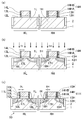
- FIGS. 5A to 5C are diagrams showing steps of forming a low threshold voltage (Lvt) transistor and a high threshold voltage (Hvt) transistor having different threshold voltages.
- the surface portion of the semiconductor substrate 101 is partitioned by STI (Shallow Trench Isolation) 102 which is element isolation, and an Lvt transistor formation region RL and an Hvt transistor formation region RH are provided.
- STI Shallow Trench Isolation
- a resist 103 covering the Hvt transistor formation region RH is formed, and channel implantation is performed on the Lvt transistor formation region RL using the resist 103 as a mask. As a result, the channel layer 104L is formed in the active region of the Lvt transistor formation region RL. Thereafter, the resist 103 is removed.
- a resist 105 covering the Lvt transistor formation region RL is formed, and channel implantation is performed on the Hvt transistor formation region RH using the resist 105 as a mask. As a result, the channel layer 104H is formed in the active region of the Hvt transistor formation region RH. Thereafter, the resist 105 is removed.
- a gate structure 109 including the gate insulating film 106, the gate electrode 107, and the sidewall spacer 108 is formed as shown in FIG. 5C. Further, impurity implantation is performed using the gate structure 109 as a mask, and an extension region 110 and a halo region 111 covering the lower side are formed on both sides of the gate structure 109. Although illustration is omitted, formation of source / drain regions and the like is also performed thereafter.
- the impurity concentrations and types of the channel layers 104L and 104H can be individually set.
- threshold voltages can be individually set for both the Lvt transistor and the Hvt transistor.
- a first field effect transistor and a second field effect transistor having the same conductivity type are formed on a substrate, and the first field effect transistor is formed on a first active region in the substrate.
- the formed first gate electrode, the first sidewall spacer formed on the side of the first gate electrode, and the first conductivity type first formed on both sides of the first active region sandwiching the lower side of the first gate electrode.
- the second field effect transistor includes a second gate electrode formed on the second active region of the substrate, a second sidewall spacer formed on a side of the second gate electrode, A second extension region of the first conductivity type formed on both sides of the second active region sandwiching the lower side of the second gate electrode, and the second field effect transistor includes:
- the threshold voltage is higher than that of the field effect transistor, and the length in the gate length direction where the first extension region and the first gate electrode overlap is longer than the length in the gate length direction where the second extension region and the second gate electrode overlap.
- the distance between the first gate electrode and the first sidewall spacer is longer than the distance between the second gate electrode and the second sidewall spacer.
- an effective gate length between the first field effect transistor and the second field effect transistor (due to the difference in the length in the gate length direction of the portion where the extension region overlaps the gate electrode ( The distances between the extension regions provided on both sides of the gate electrode are different. Therefore, the threshold voltage of the first field effect transistor is lower than the threshold voltage of the second field effect transistor. Further, as will be described later, the first extension region and the second extension region can be formed by impurity implantation using a common mask, and an increase in the mask process can be avoided.
- a first offset spacer is provided between the first sidewall spacer and the first gate electrode, and is thicker than the first offset spacer between the second sidewall spacer and the second gate electrode.
- a second offset spacer is preferably provided.
- At least the second offset spacer of the first offset spacer and the second offset spacer has a laminated structure of two or more layers, and the number of laminated second offset spacers is larger than the number of laminated first offset spacers. A large amount is preferable.
- the first offset spacer may have a single layer structure.
- the first sidewall spacer is in contact with the side wall of the first gate electrode, and an offset spacer is preferably provided between the second sidewall spacer and the second gate electrode.
- the length in the gate length direction where the first extension region and the first gate electrode overlap is preferably longer than the length in the gate length direction where the second extension region and the second gate electrode overlap by a predetermined distance.
- the distance between the first gate electrode and the first sidewall spacer is preferably shorter than the distance between the second gate electrode and the second sidewall spacer by a predetermined distance.
- the predetermined distance is preferably set by the difference between the threshold voltage of the first field effect transistor and the threshold voltage of the second field effect transistor.
- the difference in the effective gate length is generated for each field effect transistor due to the difference in the predetermined distance, and the difference in the threshold voltage is generated depending on the difference in the gate length. Therefore, the predetermined distance is set in accordance with a desired threshold voltage difference.
- the predetermined distance may be 2 nm or more and 4 nm or less. As one specific example, this may be used.
- the dimension of the first gate electrode in the gate length direction and the dimension of the second gate electrode in the gate length direction are formed to be substantially the same dimension.
- substantially the same dimension means that the design dimensions are the same, and variations occurring in the manufacturing process are included.
- the distance between the first extension regions below the first gate electrode is preferably shorter than the distance between the second extension regions below the second gate electrode.
- a second conductivity type first halo region provided between the first extension region and the substrate, and a second conductivity type second halo region provided between the second extension region and the substrate are provided. It is preferable to further provide.
- These components may be provided as a semiconductor device.
- a manufacturing method of the first semiconductor device of the present disclosure including the first field effect transistor including the first gate electrode and the second field effect transistor including the second gate electrode is performed on the first active region in the substrate.
- First impurity implantation is performed on the region to form first extension regions of the first conductivity type on both sides of the first gate electrode in the first active region.
- First impurity implantation is performed on the second active region using the second gate electrode and the second offset spacer as a mask, and second extension regions of the first conductivity type are formed on both sides of the second gate electrode in the second active region.
- the distance that the extension region extends from the end of the offset spacer to the gate electrode side is the first field effect transistor and the second electric field.
- the second offset spacer is thicker than the first offset spacer, the length in the gate length direction where the first extension region and the first gate electrode overlap with each other is the second extension region and the second gate electrode. Longer than the length in the gate length direction. As a result, the threshold voltage of the second field effect transistor becomes higher than the threshold voltage of the first field effect transistor.
- a plurality of field effect transistors having different threshold voltages can be formed by using the same impurity implantation process and without increasing the mask process.
- the second offset spacer of the first offset spacer and the second offset spacer has a laminated structure of two or more layers, and the number of laminated second offset spacers is larger than the number of laminated first offset spacers. Is preferred.
- a manufacturing method of the second semiconductor device of the present disclosure including the first field effect transistor including the first gate electrode and the second field effect transistor including the second gate electrode is performed on the first active region in the substrate.
- a first impurity is implanted into the first active region using the first gate electrode as a mask, and first extension regions of the first conductivity type are formed on both sides of the first gate electrode in the first active region.
- the first impurity implantation is performed on the second active region using the second gate electrode and the offset spacer as a mask, and both the second gate electrodes in the second active region are formed.
- impurity implantation is performed in the same step (c).
- the offset spacer is provided on the side wall of the second gate electrode and the offset spacer is not provided on the side wall of the first gate electrode, the length in the gate length direction where the first extension region and the first gate electrode overlap with each other. This is longer than the length in the gate length direction where the second extension region and the second gate electrode overlap.
- a plurality of field effect transistors having different threshold voltages can be formed by using the same impurity implantation process and without increasing the mask process.
- a first sidewall spacer and a second sidewall spacer are formed on the sides of the first gate electrode and the second gate electrode, respectively.
- second impurity implantation is performed on the first active region and the second active region, so that the first conductivity type second electrode is formed outside the first sidewall spacer when viewed from the first gate electrode in the first active region.
- One source / drain region may be formed, and a second source / drain region of the first conductivity type may be formed outside the second sidewall spacer when viewed from the second gate electrode in the second active region.
- source / drain regions can be formed for the first field effect transistor and the second field effect transistor.
- the effective gate lengths of a plurality of field effect transistors can be made different from each other by the same impurity implantation. Accordingly, a plurality of field effect transistors having different threshold voltages can be formed while avoiding an increase in the mask process.
- FIGS. 1A to 1C are diagrams schematically illustrating an exemplary semiconductor device and a manufacturing method thereof according to the first embodiment of the present disclosure.
- 2A to 2C are diagrams schematically illustrating an exemplary semiconductor device and a manufacturing method thereof according to the first embodiment of the present disclosure following FIG. 1C.
- 3A to 3C are diagrams schematically illustrating an exemplary semiconductor device and a manufacturing method thereof according to the second embodiment of the present disclosure.
- 4A to 4C are diagrams schematically illustrating an exemplary semiconductor device and a manufacturing method thereof according to the first embodiment of the present disclosure following FIG. 3C.
- 5 (a) to 5 (c) are diagrams showing a method for manufacturing a semiconductor device according to the background art.
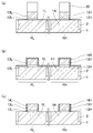
- FIGS. 1A to 1C and FIGS. 2A to 2C are diagrams schematically showing a structure of an exemplary semiconductor device 10 of this embodiment and a manufacturing method thereof.
- the semiconductor device 10 is formed using a substrate 1 which is a semiconductor substrate made of silicon or the like.
- an active region made of the substrate 1 is defined by an element isolation region 2 made of a silicon oxide film formed by, for example, a LOCOS (Local Oxidation of Silicon) method or an STI (Shallow Trench Isolation) method.
- LOCOS Local Oxidation of Silicon
- STI Shallow Trench Isolation
- Lvt transistor region RL in which a field effect transistor having a low threshold voltage (hereinafter referred to as Lvt transistor) is formed, and a field effect transistor having a threshold voltage higher than that of the Lvt transistor (hereinafter referred to as Lvt transistor).
- Lvt transistor a field effect transistor having a low threshold voltage
- Lvt transistor a field effect transistor having a threshold voltage higher than that of the Lvt transistor
- An Hvt transistor region RH in which an Hvt transistor is called is shown.
- an N-type FET is used as the Lvt transistor and the Hvt transistor.
- a gate electrode 13L is formed on the active region 1L surrounded by the element isolation region 2 in the P-type substrate 1 via a gate insulating film 12L.
- a side wall spacer 15L is formed on the side wall of the gate electrode 13L via an offset spacer 14L.
- N-type source / drain regions 16L (the source region and the drain region are collectively referred to in this way) are formed on both sides of the gate electrode 13L in the active region 1L (outside of the sidewall spacer 15L).
- N-type extension regions 17L are formed on both sides of the channel formation region below the gate electrode 13L in the active region 1L, inside the source / drain region 16L (on the gate electrode 13L side).
- the extension region 17L extends partly from both sides of the gate electrode 13L to below the gate electrode 13L. Between the extension region 17L and the substrate 1, a P-type halo region 18L having a conductivity type different from that of the extension region 17L is formed. The halo region 18L is formed so as to cover the bottom surface and the side surface (excluding the side surface connected to the source / drain region 16L) of the extension region 17L.
- the gate structure 11L of the Lvt transistor is configured by the gate insulating film 12L, the gate electrode 13L, the offset spacer 14L, and the sidewall spacer 15L.
- an Hvt transistor having a structure similar to the Lvt transistor in the Lvt transistor region RL is formed in the Hvt transistor region RH.
- the gate electrode 13H is formed on the active region 1H surrounded by the element isolation region 2 in the P-type substrate 1 via the gate insulating film 12H.
- a side wall spacer 15H is formed on the side wall of the gate electrode 13H via an offset spacer 14H.
- N-type source / drain regions 16H are formed on both sides of the gate electrode 13H in the active region 1H, and an N-type extension region 17H extending partially below the gate electrode 13H is formed on the inside thereof. Yes.
- a P-type halo region 18H having a conductivity type different from that of the extension region 17H is formed between the extension region 17H and the substrate 1.
- the halo region 18H is formed so as to cover the bottom surface and the side surface (excluding the side surface connected to the source / drain region 16H) of the extension region 17H.
- the gate structure 11H of the Hvt transistor is configured by the gate insulating film 12H, the gate electrode 13H, the offset spacer 14H, and the sidewall spacer 15H.
- the offset spacer 14H in the Hvt transistor has a two-layered structure including a first layer 14HA having an L-shaped cross-section in contact with the side wall of the gate electrode 13H and a second layer 14HB stacked on the first layer 14HA. It is a structure, and the combined thickness of the two layers is thicker than the single-layer offset spacer 14L in the Lvt transistor.
- the length of the extension region 17L (the amount of overlap with the gate electrode 13L) of the portion extending below the gate electrode 13L in the Lvt transistor is DL, and the portion of the Hvt transistor extending below the gate electrode 13H is DL. If the length of the extension region 17H is DH, DL is longer than DH. In other words, the length DL where the gate electrode 13L and the extension region 17L overlap is longer than the length DH where the gate electrode 13H and the extension region 17H overlap.
- the extension region 17L in the Lvt transistor extends further to the inside of the gate electrode than the extension region 17H in the Hvt transistor.
- the dimension in the gate length direction of the gate electrode 13L and the dimension in the gate length direction of the gate electrode 13H are substantially the same dimension. “Substantially the same dimension” means that the design dimensions are the same, and variations occurring in the manufacturing process are included.
- the distance (effective gate length) between the extension regions 17L below the gate electrode 13L of the Lvt transistor is shorter than the distance between the extension regions 17H below the gate electrode 13H of the Hvt transistor.
- the threshold voltage of the Lvt transistor is lower than the threshold voltage of the Hvt transistor.
- the difference between the overlap amount DL and the overlap amount DH is realized by the difference between the thickness of the offset spacer 14L and the thickness of the offset spacer 14H.
- the Lvt transistor formed in the Lvt transistor region RL is a transistor in which high-speed operation is more important than reduction of off-leakage current (GIDL, BTBT, etc. can be ignored). Therefore, the offset spacer 14L is set thin and the threshold voltage is low so that the overlap amount DL is sufficiently long.
- the Hvt transistor formed in the Hvt transistor region RH is a transistor that emphasizes reduction of off-leakage current as compared with the Lvt transistor (GIDL, BTBT, etc. cannot be ignored). Therefore, in order to shorten the overlap amount DH (compared to the overlap amount DL), the offset spacer 14H is set thicker than the offset spacer 14L. However, the extension region 17H is not offset with respect to the gate electrode 13H (the arrangement is such that it does not enter below the gate electrode 13H).
- the amount of overlap between the extension region and the gate electrode can be determined, and the threshold voltage of each transistor can be set.
- FIG. 1 (a) shows a state where the gate electrode is formed.
- a P-type substrate 1 which is a semiconductor substrate made of P-type single crystal silicon, a semiconductor substrate made of single-crystal silicon in which a P-type well region is formed, and the like, for example, B (boron) ions which are P-type impurities, etc. Inject. This is performed under predetermined conditions for injecting into the channel formation region on the surface of the substrate 1. Thereafter, a P-type channel diffusion layer is formed by heat treatment (not shown).
- an Lvt transistor region RL for forming a field effect transistor with a low threshold voltage and an Hvt transistor region RH for forming a field effect transistor with a high threshold voltage are determined, and the channel formation region of the substrate 1 is locally Expose.
- an element isolation region 2 is formed on the surface of the substrate 1 by the LOCOS method, the STI method, or the like. Thereby, an active region 1L and an active region 1H made of the substrate 1 surrounded by the element isolation region 2 are formed.
- an insulating film to be the gate insulating films 12L and 12H is formed so as to cover the substrate 1, and an electrode material layer to be the gate electrodes 13L and 13H is further formed thereon.
- the insulating film can be a single layer film or a laminated film of SiO 2 , SiON, HfSiO, HfSiON, HfO 2 or the like.
- a thermal oxidation method a physical vapor deposition method (hereinafter referred to as a PVD (Physical Vapor Deposition) method), a chemical vapor deposition method (hereinafter referred to as a CVD (Chemical Vapor Deposition) method), or the like is used. be able to.
- the electrode material layer may be a single layer structure of a metal material such as Ta, TaN, Ti, TiN, Al, TiAl, or a laminated structure thereof.
- a laminated structure of a metal layer made of any of the aforementioned metal materials and a Si layer formed on the metal layer or a Si-containing layer made of a material containing Si may be used.
- a PVD method, a CVD method, a sputtering method, or the like can be used.
- the resist 20 is formed by patterning so as to correspond to the formation positions of the gate electrode 13L in the Lvt transistor region RL and the gate electrode 13H in the Hvt transistor region RH. Subsequently, the electrode material layer and the insulating film are etched using the resist 20 as a mask to form the gate insulating film 12L and the gate electrode 13L on the active region 1L in the Lvt transistor region RL, while the active in the Hvt transistor region RH. A gate insulating film 12H and a gate electrode 13H are formed on the region 1H. Thereafter, the resist 20 is removed.
- an insulating film serving as an offset spacer is formed on the entire surface of the substrate 1 so as to cover the upper surfaces and side surfaces of the gate electrodes 13L and 13H.
- an insulating film 14A made of SiN is deposited to a thickness of 2 nm to 10 nm
- an insulating film 14B made of an SiO 2 film is deposited to a thickness of 2 nm to 10 nm so as to cover the insulating film 14A.
- a CVD method or the like may be used as a formation method.
- the insulating film 14A is an SiN film and the insulating film 14B is an SiO 2 film, but these materials may be reversed. In addition, other materials can be used as long as the insulating film 14B can be selectively removed with respect to the insulating film 14A.
- a resist material is applied to the entire surface of the substrate 1 and then patterned so that only the Hvt transistor region RH is masked to form a resist 21. Thereafter, wet etching is performed using the resist 21 as a mask, and only the insulating film 14B in the Lvt transistor region RL is selectively removed. Thereafter, the resist 21 is removed. As a result, the insulating film 14B on the active region 1L is removed and only the insulating film 14A remains, and both the insulating film 14A and the insulating film 14B remain on the active region 1H.
- an offset spacer 14L having a single layer structure is formed from the insulating film 14A on the side of the gate electrode 13L in the Lvt transistor region RL. Further, on the side of the gate electrode 13H in the Hvt transistor region RH, a first layer 14HA having an L-shaped cross-sectional shape made of an insulating film 14A and a second layer 14HB formed on the first layer 14HA are formed. An offset spacer 14H having a two-layer structure is formed.
- the offset spacer 14H in the Hvt transistor region RH has a structure in which the second layer 14HB is laminated on the first layer 14HA made of the same insulating film 14A as the offset spacer 14L in the Lvt transistor region RL. The thickness is increased by the thickness of the two layers 14HB.
- extension regions and halo regions are formed.
- ions of As or P which are N-type impurities are implanted.
- the implantation conditions for example, when the implanted ion is As, the implantation energy is 2 keV, the dose is 1 to 2 ⁇ 10 15 / cm 2 , and the implantation angle is 0 ° (with respect to the normal of the main surface of the substrate 1). The angle formed is 0 °).
- the gate electrode 13L and the offset spacer 14L serve as a mask so that the N-type extension region 17L overlaps the active region 1L below the gate electrode 13L by the overlap amount DL. Formed.
- the gate electrode 13H and the offset spacer 14H thicker than the offset spacer 14L in the Lvt transistor region RL serve as a mask, and the N-type extension region 17H is formed in the active region 1H. It is formed to overlap with the overlap amount DH below 13H.
- the offset spacer 14L is thinner than the offset spacer 14H, even if extension implantation is similarly performed on the Lvt transistor region RL and the Hvt transistor region RH, the overlap amount DL is larger than the overlap amount DH. become longer. Therefore, it is not necessary to separately perform extension implantation for the Lvt transistor region RL and the Hvt transistor region RH for the purpose of providing a difference in effective gate length. Therefore, a plurality of field effect transistors having different threshold voltages can be provided on the same substrate without increasing the mask process.
- P-type halo regions 18L and 18H are formed so as to cover the lower portions of the extension regions 17L and 17H, respectively, and be positioned between the substrate 1 and the P-type halo regions 18L and 18H.
- B, BF 2 or In is ion-implanted as a P-type impurity.
- the implantation conditions for example, when the implanted ion is B, the implantation energy is 5 to 10 keV, the dose is 1 to 4 ⁇ 10 13 / cm 2 , and the implantation angle is 15 to 38 °.
- the difference in threshold voltage between the Lvt transistor having a low threshold voltage and the Hvt transistor having a high threshold voltage is an effective gate length (distance between the extension regions below the gate electrode) of the Lvt transistor and the Hvt transistor. Realized by differences. Since the effective gate length difference is determined by the difference between the overlap amounts DL and DH, the difference in the thickness of the offset spacer is set in accordance with the required difference in gate length.
- the difference in threshold voltage between the Lvt transistor having a low threshold voltage and the Hvt transistor having a high threshold voltage is preferably about 50 to 100 mV, for example.
- the threshold voltage varies by 100 mV.
- the thickness of the offset spacer is also set to a difference of 2 nm to 4 nm (4 nm to 8 nm in total) on both sides of the gate electrode so that a difference of 4 nm to 8 nm appears in the effective gate length. That is, the offset spacer 14H in the Hvt transistor region RH is set to be 2 nm to 4 nm thicker than the offset spacer 14L in the Lvt transistor region RL. In other words, the film thickness of the second layer 14HB in the offset spacer 14H may be 2 nm to 4 nm.
- the overlap amount DH becomes 2 nm to 4 nm (more than the overlap amount DL) on both sides of the gate electrode 13H, and the effective gate length difference can be 4 nm to 8 nm.
- the above numerical value is a desirable example when the gate length direction of the gate electrodes 13L and 13H itself is about 40 nm, but is not limited thereto. It can be set based on the dimensions of the gate electrode, the concentration of various impurity regions (extension regions, source / drain regions, etc.), the desired threshold voltage difference, and the like.
- an insulating film made of a single layer film of SiO 2 film, SiN film or SiON film, or a laminated film thereof is formed on the substrate 1 so as to cover the gate electrode 13L, the gate electrode 13H, and the like.
- anisotropic dry etching is performed on the insulating film, and other portions are removed except for the lateral portions of the gate electrode 13L and the gate electrode 13H.
- the side wall spacer 15L is formed on the side of the gate electrode 13L via the offset spacer 14L, while the side wall spacer 15H is formed on the side of the gate electrode 13H via the offset spacer 14H.
- the distance between the gate electrode 13L and the side wall spacer 15L is shorter than the distance between the gate electrode 13H and the side wall spacer 15H.
- the gate structure 11L is formed in the Lvt transistor region RL, and the gate structure 11H is formed in the Hvt transistor region RH.
- N-type impurities such as As are ion-implanted into the active region 1L and the active region 1H, thereby forming N-type on both sides of the gate structure 11L and the gate structure 11H, respectively.
- Source / drain regions 16L and 16H are formed.
- the semiconductor device 10 including the Lvt transistor and the Hvt transistor is formed on the same substrate. According to such a manufacturing method, field effect transistors having different threshold voltages can be formed without increasing the mask process, and the manufacturing process can be shortened.
- the offset spacer 14H thicker than the offset spacer 14L having a single-layer structure by using a two-layer structure
- a difference in thickness may be provided by other methods.
- the offset spacer 14L may also be provided with an offset spacer 14H having a larger number of layers as a structure having a plurality of layers.
- an Mvt transistor having an intermediate threshold voltage may be provided in addition to the Lvt transistor and the Hvt transistor.
- an offset spacer having an intermediate thickness between the offset spacer 14L and the offset spacer 14H is provided in this case.
- the present invention can be applied to the case where an SRAM transistor or the like is provided.
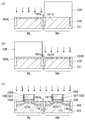
- FIGS. 3A to 3C and FIGS. 4A to 4C are views schematically showing the structure of the exemplary semiconductor device 10a of the present embodiment and the manufacturing method thereof.
- the same reference numerals as those in FIG. 2C are used for the same components as those of the semiconductor device 10 of the first embodiment, and the differences will be described in detail below.
- a gate electrode 13L is formed on the active region 1L surrounded by the element isolation region 2 in the P-type substrate 1 via a gate insulating film 12L.
- a side wall spacer 15L is formed on the side of the gate electrode 13L in contact with the side wall of the gate electrode 13L without using an offset spacer.
- the gate structure 11L of the Lvt transistor region RL is configured by the gate insulating film 12L, the gate electrode 13L, and the sidewall spacer 15L.
- an N-type extension region 17L is formed so as to overlap with the overlap amount DL below the gate electrode 13L.
- An N-type source / drain region 16L is formed outside the extension region 17L, and a P-type halo region 18L is formed between the extension region 17L and the substrate 1 so as to cover the lower side of the extension region 17L. Has been.
- a gate electrode 13H is formed on the active region 1H surrounded by the element isolation region 2 in the P-type substrate 1 via the gate insulating film 12H.
- a side wall spacer 15H is formed on the side of the gate electrode 13H via an offset spacer 14H.
- the gate structure 11H of the Hvt transistor region RH is configured by the gate insulating film 12H, the gate electrode 13H, the offset spacer 14H, and the sidewall spacer 15H.
- an N-type extension region 17H is formed so as to overlap with the overlap amount DH below the gate electrode 13H.
- An N-type source / drain region 16H is formed outside the extension region 17H, and a P-type halo region 18H is formed between the extension region 17H and the substrate 1 so as to cover the extension region 17H. Has been.
- the overlap amount DL in the Lvt transistor is longer than the overlap amount DH in the Hvt transistor.
- the distance (effective gate length) between the extension regions 17L below the gate electrode 13L of the Lvt transistor is shorter than the distance between the extension regions 17H below the gate electrode 13H of the Hvt transistor.
- the threshold voltage of the Lvt transistor is lower than the threshold voltage of the Hvt transistor.
- the difference between the overlap amount DL and the overlap amount DL is realized by not providing the offset spacer in the Lvt transistor and providing the offset spacer 14H in the Hvt transistor.
- FIG. 3 (a) shows a state where the gate electrode is formed. This may be formed in the same manner as described with reference to FIG. 1A in the first embodiment. After obtaining the configuration of FIG. 3A, the resist 20 is removed.
- an insulating film 14A serving as an offset spacer is formed so as to cover the upper surface and side surfaces of the gate electrode 13L and the gate electrode 13H.
- a SiN film, a SiO 2 film, or the like is used and formed to a thickness of 2 nm to 10 nm by a CVD method.
- anisotropic etching is performed on the entire surface of the substrate 1 to etch back the entire surface of the insulating film 14A, leaving only the portions covering the side walls of the gate electrodes and other portions.
- an offset spacer is formed. More specifically, an offset spacer 14H that covers the side wall of the gate electrode 13H in the Hvt transistor region RH is formed. Also in the Lvt transistor region RL, an offset spacer 14L that covers the side wall of the gate electrode 13L is formed.
- the offset spacer 14L in the Lvt transistor region RL is removed.
- resist is applied and patterned as a resist 21 covering only the Hvt transistor region RH.
- Wet etching is performed using the resist 21 as a mask, and the offset spacer 14L in the Lvt transistor region RL is selectively removed. Thereafter, the resist 21 is removed.
- an N-type extension region and a P-type halo region are formed.
- As or P that is an N-type impurity is ion-implanted under the same conditions as described in the first embodiment.
- the extension region 17L is formed in the active region 1L.
- the extension region 17L is formed to overlap with the overlap amount DL below the gate electrode 13L.
- the gate electrode 13H and the offset spacer 14H serve as a mask.
- the extension region 17H is formed to overlap the overlap amount DH below the gate electrode 13H.
- the offset spacer 14H is formed only in the Hvt transistor region RH, the overlap amount DL is longer than the overlap amount DH even if extension implantation is similarly performed on the Lvt transistor region RL and the Hvt transistor region RH. Become. Therefore, it is possible to provide a difference in effective gate length between the Lvt transistor and the Hvt transistor without requiring a separate mask process and implantation process, and a plurality of field effect transistors having different threshold voltages can be formed on the same substrate. Can be provided.
- the halo regions 18L and 18H are formed so as to cover the lower portions of the extension regions 17L and 17H, respectively, and to be positioned between the substrate 1 and the substrate.
- B, BF 2 or In is ion-implanted as a P-type impurity.
- the injection conditions may be the same as those in the first embodiment.
- the thickness of the offset spacer 14H in the Hvt transistor region RH is set in accordance with a necessary difference in gate length.
- the desired threshold voltage difference between the Lvt transistor and the Hvt transistor is about 50 to 100 mV. Further, it is assumed that the threshold voltage fluctuates by 100 mV with respect to an effective gate length fluctuation of 8 nm. In such a case, the effective gate length difference between the Lvt transistor and the Hvt transistor may be 4 nm to 8 nm. Therefore, the thickness of the offset spacer 14H may be formed to 2 nm to 4 nm.
- the overlap amount DH is increased by 2 nm to 4 nm on both sides of the gate electrode 13H (more than the overlap amount DL), and the effective gate length difference can be 4 nm to 8 nm.
- these numerical values are merely examples, and can be set based on the dimensions of the gate electrode, the concentrations of various impurity regions, the desired threshold voltage difference, and the like.
- an insulating film is formed on the substrate 1 so as to cover the gate electrode 13L, the gate electrode 13H, and the like, and anisotropic dry etching is performed on the insulating film to thereby form a sidewall spacer in contact with the side surface of the gate electrode 13L.
- 15L and a sidewall spacer 15H formed on the side of the gate electrode 13H via an offset spacer 14H are obtained.
- the gate structure 11L is formed in the Lvt transistor region RL, and the gate structure 11H is formed in the Hvt transistor region RH.
- N-type impurities such as As are ion-implanted into the active region 1L and the active region 1H, thereby forming N-type on both sides of the gate structure 11L and the gate structure 11H, respectively.
- Source / drain regions 16L and 16H are formed.
- the semiconductor device 10a is formed. According to such a manufacturing method, field effect transistors having different threshold voltages can be formed without increasing the mask process, and the manufacturing process can be shortened.
- the overlap amount between the gate electrode and the extension region can be set to three or more by one extension injection.
- each of the first and second embodiments an N-channel transistor has been described as an example. However, each configuration can be applied to a P-channel transistor.
- channel injection may be performed separately for the Lvt transistor and the Hvt transistor. As a result, the number of steps related to channel implantation increases, but the controllability of the threshold voltage can be further improved.
- the technology of the present disclosure it is possible to realize a semiconductor device including a plurality of field effect transistors having different threshold voltages and a method for manufacturing the same while suppressing an increase in manufacturing steps, and also for miniaturization of a semiconductor device. It is possible.
Abstract
半導体装置は同一導電型の第1及び第2FETを有する。第1FETは、基板1上の第1ゲート電極(13L)、その側方の第1サイドウォール(15L)、第1ゲート電極(13L)両側の第1活性領域(1L)の第1エクステンション領域(17L)を備える。第2FETは、基板1上の第2ゲート電極(13H)、その側方の第2サイドウォール(15H)、第2ゲート電極(13H)両側の第2活性領域(1H)の第2エクステンション領域(17H)を備える。ゲート長方向に関し、第1エクステンション領域(17L)と第1ゲート電極(13L)との重なりは、第2エクステンション領域(17H)と第2ゲート電極(13H)との重なりよりも長い。第1ゲート電極(13L)と第1サイドウォール(15L)との距離は、第2ゲート電極(13H)と第2サイドウォール(15H)との距離より短い。
Description
本発明は半導体装置とその製造方法に関し、特に、異なる閾値電圧を有する複数の電界効果型トランジスタ(Field Effect Transistor,FET)を備えた半導体装置とその製造方法に関する。
近年、半導体装置の高集積化を実現するために、個々の半導体素子の微細化が行なわれてきている。微細化が進むに連れて、異なる閾値電圧を有する複数の電界効果トランジスタ(以下、単にトランジスタと呼ぶことがある)を備える半導体装置(例えばeSRAM(embedded Static Random Access Memory))において、それぞれのトランジスタの閾値電圧を同時に最適化することが困難になってきている。
そこで、同一基板上に閾値電圧の異なる複数のトランジスタを含む半導体装置において、それぞれの閾値電圧の調整方法が種々提案されている。その一つについて、以下に説明する。
図5(a)~(c)は、互いに閾値電圧の異なる低閾値電圧(Lvt)トランジスタ及び高閾値電圧(Hvt)トランジスタを形成する工程を示す図である。これらの図に示すように、半導体基板101の表面部が素子分離であるSTI(Shallow Trench Isolation)102により区画され、Lvtトランジスタ形成領域RLと、Hvtトランジスタ形成領域RHとが設けられている。
まず、図5(a)に示すように、Hvtトランジスタ形成領域RHを覆うレジスト103を形成し、該レジスト103をマスクとしてLvtトランジスタ形成領域RLに対してチャネル注入を行なう。これにより、Lvtトランジスタ形成領域RLの活性領域にチャネル層104Lが形成される。この後、レジスト103を除去する。
次に、図5(b)に示すように、Lvtトランジスタ形成領域RLを覆うレジスト105を形成し、該レジスト105をマスクとしてHvtトランジスタ形成領域RHに対してチャネル注入を行なう。これにより、Hvtトランジスタ形成領域RHの活性領域にチャネル層104Hが形成される。この後、レジスト105を除去する。
図5(b)の工程の後、図5(c)のように、ゲート絶縁膜106、ゲート電極107及びサイドウォールスペーサー108を含むゲート構造109を形成する。更に、ゲート構造109をマスクとして不純物注入を行ない、ゲート構造109の両側にエクステンション領域110及びその下方を覆うハロー領域111とを形成する。図示は省略するが、この後、ソース/ドレイン領域等の形成も行なわれる。
以上のように、Lvtトランジスタ形成領域RLとHvtトランジスタ形成領域RHとに対して別々にチャネル注入を行なうことにより、それぞれのチャネル層104L及び104Hの不純物の濃度、種類を個別に設定することができる。この結果、Lvtトランジスタ及びHvtトランジスタの両方について、閾値電圧を個別に設定することができる。
しかしながら、チャネル層の不純物について設定するだけでは、Lvtトランジスタ及びHvtトランジスタのそれぞれの性能向上に限度がある。これに対し、チャネル注入に加えて、エクステンション注入についてもトランジスタの種類毎に個別に行なうことは可能である。しかし、そのためにはマスク工程、注入工程をそれぞれ個別に行なうことを要し、製造工程が長くなってしまう。
以上に鑑み、閾値電圧の異なる複数のトランジスタを備える半導体装置及びその製造方法において、マスク工程の増加を抑えながら、それぞれのトランジスタの性能を向上する技術について以下に説明する。
本開示の半導体装置は、基板上に、同一の導電型である第1電界効果型トランジスタ及び第2電界効果型トランジスタが形成され、第1電界効果型トランジスタは、基板における第1活性領域上に形成された第1ゲート電極と、第1ゲート電極の側方に形成された第1サイドウォールスペーサーと、第1活性領域における第1ゲート電極下方を挟む両側に形成された第1導電型の第1エクステンション領域とを備え、第2電界効果型トランジスタは、基板における第2活性領域上に形成された第2ゲート電極と、第2ゲート電極の側方に形成された第2サイドウォールスペーサーと、第2活性領域における第2ゲート電極下方を挟む両側に形成された第1導電型の第2エクステンション領域とを備え、第2電界効果型トランジスタは、第1電界効果型トランジスタよりも閾値電圧が高く、第1エクステンション領域と第1ゲート電極とが重なるゲート長方向の長さは、第2エクステンション領域と第2ゲート電極とが重なるゲート長方向の長さよりも長く、第1ゲート電極と第1サイドウォールスペーサーとの間の距離は、第2ゲート電極と第2サイドウォールスペーサーとの間の距離よりも短い。
このような半導体装置によると、エクステンション領域がゲート電極と重なっている部分のゲート長方向の長さの違いにより、第1電界効果型トランジスタと第2電界効果型トランジスタとでは実効的なゲート長(それぞれゲート電極の両側に設けられているエクステンション領域間の距離)が異なる。このことから、第1電界効果型トランジスタの閾値電圧は、第2電界効果型トランジスタの閾値電圧よりも低くなっている。また、後に説明する通り、共通のマスクを用いた不純物注入によって第1エクステンション領域と第2エクステンション領域を形成することができ、マスク工程の増加を避けることができる。
尚、第1サイドウォールスペーサーと、第1ゲート電極との間に、第1オフセットスペーサーが設けられ、第2サイドウォールスペーサーと、第2ゲート電極との間に、第1のオフセットスペーサーよりも厚い第2オフセットスペーサー設けられていることが好ましい。
ゲート電極とサイドウォールスペーサーとの間の距離の差(第1電界効果型トランジスタにおいて、第2電界効果型トランジスタにおけるよりも短い)を実現するために、このようにしても良い。
ここで、記第1オフセットスペーサー及び第2オフセットスペーサーのうちの少なくとも第2オフセットスペーサーは、2層以上の積層構造であり、第2オフセットスペーサーの積層数は、第1オフセットスペーサーの積層数よりも多いことが好ましい。
第2オフセットスペーサーを第1オフセットスペーサーよりも厚くするために、このようにしてもよい。この場合、第1オフセットスペーサーについては単層構造であっても良い。
また、第1サイドウォールスペーサーは、第1ゲート電極の側壁に接しており、第2サイドウォールスペーサーと、第2ゲート電極との間に、オフセットスペーサーが設けられていることが好ましい。
ゲート電極とサイドウォールスペーサーとの間の距離の差を実現するために、このようにすることもできる。
また、第1エクステンション領域と第1ゲート電極とが重なるゲート長方向の長さは、第2エクステンション領域と第2ゲート電極とが重なるゲート長方向の長さよりも所定の距離だけ長いことが好ましい。
また、第1ゲート電極と第1サイドウォールスペーサーとの間の距離は、第2ゲート電極と第2サイドウォールスペーサーとの間の距離よりも所定の距離だけ短いことが好ましい。
また、所定の距離は、第1電界効果型トランジスタの閾値電圧と第2電界効果型トランジスタの閾値電圧との違いによって設定されていることが好ましい。
それぞれ所定の距離の差により、電界効果型トランジスタ毎に実効的なゲート長の差が生じ、該ゲート長の差に依存して、閾値電圧の差が生じる。よって、望ましい閾値電圧の差に合わせて、前記所定の距離を設定する。
所定の距離は、2nm以上で且つ4nm以下であってもよい。具体例の1つとして、このようにしても良い。
また、第1ゲート電極のゲート長方向の寸法と、第2ゲート電極のゲート長方向の寸法とは実質的に同一寸法に形成されていることことが好ましい。
ここで、実質的に同一寸法とは、設計寸法が同じであり、製造過程において生じるバラツキは含むことを意味する。
また、第1ゲート電極の下方における第1エクステンション領域間の距離は、第2ゲート電極の下方における第2エクステンション領域間の距離よりも短いことが好ましい。
ゲート電極自体の寸法が同じであっても、前記のようなエクステンション領域の構成の違いにより、それぞれの電界効果型トランジスタにおける実効的なゲート長に違いを設けることができる。
また、第1エクステンション領域と基板との間に設けられた第2導電型の第1ハロー領域と、第2エクステンション領域と基板との間に設けられた第2導電型の第2ハロー領域とを更に備えることが好ましい。
また、第1活性領域における第1ゲート電極から見て第1エクステンション領域の外側に形成された第1導電型の第1ソース/ドレイン領域と、第2活性領域における第2ゲート電極から見て第2エクステンション領域の外側に形成された第1導電型の第2ソース/ドレイン領域とを備えることが好ましい。
半導体装置として、これらの構成要素備えていても良い。
次に、第1ゲート電極を含む第1電界効果型トランジスタ及び第2ゲート電極を含む第2電界効果型トランジスタを備える本開示の第1の半導体装置の製造方法は、基板における第1活性領域上に第1ゲート電極を形成すると共に、基板における第2活性領域上に第2ゲート電極を形成する工程(a)と、第1ゲート電極の側壁に第1オフセットスペーサーを形成すると共に、第2ゲート電極の側壁に、第1オフセットスペーサーよりも厚さの厚い第2オフセットスペーサーを形成する工程(b)と、工程(b)の後に、第1ゲート電極及び第1オフセットスペーサーをマスクとして第1活性領域に対して第1の不純物注入を行ない、第1活性領域における第1ゲート電極の両側に第1導電型の第1エクステンション領域を形成すると共に、第2ゲート電極及び第2オフセットスペーサーをマスクとして第2活性領域に対して第1の不純物注入を行ない、第2活性領域における第2ゲート電極の両側に第1導電型の第2エクステンション領域を形成する工程(c)とを備える。
第1の半導体装置の製造方法において、同じ工程(c)にて不純物注入を行なうため、オフセットスペーサーの端からゲート電極の側にエクステンション領域が延びる距離は、第1電界効果型トランジスタ及び第2電界効果型トランジスタのどちらにおいても同じである。しかし、第1オフセットスペーサーよりも第2オフセットスペーサーの方が厚さが厚いので、第1エクステンション領域と第1ゲート電極とが重なるゲート長方向の長さは、第2エクステンション領域と第2ゲート電極とが重なるゲート長方向の長さよりも長くなる。この結果、第2電界効果型トランジスタの閾値電圧は、第1電界効果型トランジスタの閾値電圧よりも高くなる。
このように、同じ不純物注入工程を利用し、マスク工程を増加させることなく、閾値電圧の異なる複数の電界効果型トランジスタを形成することができる。
尚、第1オフセットスペーサー及び第2オフセットスペーサーのうちの少なくとも第2オフセットスペーサーは、2層以上の積層構造であり、第2オフセットスペーサーの積層数は、第1オフセットスペーサーの積層数よりも多いことが好ましい。
第2オフセットスペーサーを第1オフセットスペーサーよりも厚くするために、このようにしてもよい。
次に、第1ゲート電極を含む第1電界効果型トランジスタ及び第2ゲート電極を含む第2電界効果型トランジスタを備える本開示の第2の半導体装置の製造方法は、基板における第1活性領域上に第1ゲート電極を形成すると共に、基板における第2活性領域上に第2ゲート電極を形成する工程(a)と、第2ゲート電極の側壁にオフセットスペーサーを形成する工程(b)と、工程(b)の後に、第1ゲート電極をマスクとして第1活性領域に対して第1の不純物注入を行ない、第1活性領域における第1ゲート電極の両側に第1導電型の第1エクステンション領域を形成すると共に、第2ゲート電極及びオフセットスペーサーをマスクとして第2活性領域に対して第1の不純物注入を行ない、第2活性領域における第2ゲート電極の両側に第1導電型の第2エクステンション領域を形成する工程(c)とを備え、工程(c)において、第1ゲート電極の側壁にオフセットスペーサーが形成されていない状態で第1の不純物注入を行なう。
第2の半導体装置の製造方法においても、同じ工程(c)にて不純物注入を行なう。ここで、第2ゲート電極の側壁にはオフセットスペーサーが設けられ、第1ゲート電極の側壁にはオフセットスペーサーが設けられないため、第1エクステンション領域と第1ゲート電極とが重なるゲート長方向の長さは、第2エクステンション領域と第2ゲート電極とが重なるゲート長方向の長さよりも長くなる。このように、同じ不純物注入工程を利用し、マスク工程を増加させることなく、閾値電圧の異なる複数の電界効果型トランジスタを形成することができる。
また、第1及び第2の半導体装置の製造方法において、工程(c)の後に、第1ゲート電極及び第2ゲート電極の側方にそれぞれ第1サイドウォールスペーサー及び第2サイドウォールスペーサーを形成した後、第1活性領域及び第2活性領域に対して第2の不純物注入を行なうことにより、第1活性領域における第1ゲート電極から見て第1サイドウォールスペーサーの外側に第1導電型の第1ソース/ドレイン領域を形成すると共に、第2活性領域における第2ゲート電極から見て第2サイドウォールスペーサーの外側に第1導電型の第2ソース/ドレイン領域を形成しても良い。
このようにして、第1電界効果型トランジスタ及び第2電界効果型トランジスタについて、ソース/ドレイン領域を形成することができる。
本開示の半導体装置及びその製造方法によると、同じ不純物注入により、複数の電界効果型トランジスタにおける実効的なゲート長を互いに異なるようにすることができる。このことから、マスク工程の増加を避けながら、互いに異なる閾値電圧を有する複数の電界効果型トランジスタを形成することができる。
(第1の実施形態)
以下、本開示の第1の実施形態の半導体装置とその製造方法について、図面を参照しながら説明する。
以下、本開示の第1の実施形態の半導体装置とその製造方法について、図面を参照しながら説明する。
図1(a)~(c)及び図2(a)~(c)は、本実施形態の例示的半導体装置10の構造及びその製造方法について模式的に示す図である。図2(c)に示すように、半導体装置10は、シリコンからなる半導体基板等である基板1を用いて形成されている。基板1の表面部は、例えばLOCOS(Local Oxidation of Silicon)法やSTI(Shallow Trench Isolation)法により形成されたシリコン酸化膜からなる素子分離領域2によって基板1からなる活性領域が区画されている。図2(c)には、閾値電圧の低い電界効果型トランジスタ(以下、Lvtトランジスタと呼ぶ)が形成されたLvtトランジスタ領域RLと、Lvtトランジスタに比べて閾値電圧の高い電界効果型トランジスタ(以下、Hvtトランジスタと呼ぶ)が形成されたHvtトランジスタ領域RHとが示されている。尚、本実施形態では、Lvtトランジスタ及びHvtトランジスタとして、N型FETを用いて説明する。
Lvtトランジスタ領域RLにおいて、P型の基板1における素子分離領域2に囲まれた活性領域1L上に、ゲート絶縁膜12Lを介してゲート電極13Lが形成されている。ゲート電極13Lの側壁には、オフセットスペーサー14Lを介してサイドウォールスペーサー15Lが形成されている。また、活性領域1Lにおけるゲート電極13Lの両側方(サイドウォールスペーサー15Lの外側方)に、N型のソース/ドレイン領域16L(ソース領域及びドレイン領域をまとめてこのように呼ぶ)が形成されている。更に、ソース/ドレイン領域16Lよりも内側(ゲート電極13L側)に、N型のエクステンション領域17Lが、活性領域1Lにおけるゲート電極13L下方のチャネル形成領域を挟んで両側に形成されている。エクステンション領域17Lは、ゲート電極13Lの両側方から一部がゲート電極13Lの下方にまで延びている。エクステンション領域17Lと基板1との間に、エクステンション領域17Lとは導電型が異なるP型のハロー領域18Lが形成されている。ハロー領域18Lは、エクステンション領域17Lの底面及び側面(ソース/ドレイン領域16Lに接続している側面は除く)を覆うように形成されている。
ゲート絶縁膜12L、ゲート電極13L、オフセットスペーサー14L及びサイドウォールスペーサー15Lにより、Lvtトランジスタのゲート構造11Lが構成されている。
次に、Hvtトランジスタ領域RHには、Lvtトランジスタ領域RLのLvtトランジスタと類似した構造のHvtトランジスタが形成されている。具体的に、P型の基板1における素子分離領域2に囲まれた活性領域1H上に、ゲート絶縁膜12Hを介してゲート電極13Hが形成されている。ゲート電極13Hの側壁には、オフセットスペーサー14Hを介してサイドウォールスペーサー15Hが形成されている。また、活性領域1Hにおけるゲート電極13Hの両側方にN型のソース/ドレイン領域16Hが形成され、その内側に一部がゲート電極13Hの下方にまで延びたN型のエクステンション領域17Hが形成されている。エクステンション領域17Hと基板1との間には、エクステンション領域17Hとは導電型が異なるP型のハロー領域18Hが形成されている。ハロー領域18Hは、エクステンション領域17Hの底面及び側面(ソース/ドレイン領域16Hに接続している側面は除く)を覆うように形成されている。
ゲート絶縁膜12H、ゲート電極13H、オフセットスペーサー14H及びサイドウォールスペーサー15Hにより、Hvtトランジスタのゲート構造11Hが構成されている。
ここで、Hvtトランジスタにおけるオフセットスペーサー14Hは、ゲート電極13Hの側壁に接する断面形状がL字状の第一層14HAと、該第一層14HAに積層する第二層14HBとからなる2層の積層構造であり、2層合わせた厚さは、Lvtトランジスタにおける一層構造のオフセットスペーサー14Lよりも厚くなっている。
また、Lvtトランジスタにおいてゲート電極13Lの下方に延びている部分のエクステンション領域17Lの長さ(ゲート電極13Lとのオーバーラップ量)をDLとし、Hvtトランジスタにおいてゲート電極13Hの下方に延びている部分のエクステンション領域17Hの長さをDHとすると、DLはDHよりも長い。言い換えると、ゲート電極13Lとエクステンション領域17Lとが重なる長さDLは、ゲート電極13Hとエクステンション領域17Hとが重なる長さDHよりも長い。また、Lvtトランジスタにおけるエクステンション領域17Lは、Hvtトランジスタにおけるエクステンション領域17Hに比べると、よりゲート電極の内側にまで延びていることになる。
ここで、ゲート電極13Lのゲート長方向の寸法とゲート電極13Hのゲート長方向の寸法とは、実質的に同一寸法である。実質的に同一寸法とは、設計寸法が同じであり、製造過程において生じるバラツキは含むことを意味する。
このことから、Lvtトランジスタのゲート電極13L下方におけるエクステンション領域17L間の距離(実効的なゲート長)は、Hvtトランジスタのゲート電極13H下方におけるエクステンション領域17H間の距離よりも短くなっている。
このようにすることによって、Lvtトランジスタの閾値電圧は、Hvtトランジスタの閾値電圧に比べて低くなっている。
オーバーラップ量DLとオーバーラップ量DHとの違いは、オフセットスペーサー14Lの厚さとオフセットスペーサー14Hの厚さの違いによって実現されている。
Lvtトランジスタ領域RLに形成されるLvtトランジスタは、オフリーク電流の低減よりも動作の高速性等を重視する(GIDL、BTBT等を無視できる)トランジスタである。そこで、オーバーラップ量DLが十分に長くなるように、オフセットスペーサー14Lは薄く設定され、閾値電圧が低くなっている。
これに対し、Hvtトランジスタ領域RHに形成されるHvtトランジスタは、Lvtトランジスタに比べてオフリーク電流の低減を重視する(GIDL、BTBT等を無視できない)トランジスタである。そこで、オーバーラップ量DHを(オーバーラップ量DLに比べて)短くするために、オフセットスペーサー14Hがオフセットスペーサー14Lよりも厚く設定されている。但し、エクステンション領域17Hがゲート電極13Hに対してオフセットする(ゲート電極13Hの下方に入り込まない配置になる)ことは無いようにする。
以上のように、オフセットスペーサーの厚さをそれぞれ設定することにより、エクステンション領域とゲート電極とのオーバーラップ量を決定し、それぞれのトランジスタの閾値電圧を設定することができる。
次に、図1(a)~(c)及び図2(a)~(c)を参照して、半導体装置10の製造方法について説明する。
図1(a)には、ゲート電極の形成まで行なわれた状態が示されている。まず、P型の単結晶シリコンからなる半導体基板、P型ウェル領域が形成された単結晶シリコンからなる半導体基板等であるP型の基板1に、例えばP型不純物であるB(ホウ素)イオン等を注入する。これは、基板1表面のチャネル形成領域に注入するための所定の条件により行なう。その後、熱処理により、P型チャネル拡散層を形成する(図示省略)。
次に、閾値電圧の低い電界効果型トランジスタを形成するLvtトランジスタ領域RLと、閾値電圧の高い電界効果型トランジスタを形成するHvtトランジスタ領域RHとを定めて、基板1のチャネル形成領域を局所的に露出させる。このためには、基板1の表面部にLOCOS法、STI法等による素子分離領域2を形成する。これにより、素子分離領域2によって囲まれた基板1からなる活性領域1L及び活性領域1Hがそれぞれ形成される。
次に、基板1上を覆うように、ゲート絶縁膜12L及び12Hとなる絶縁膜を形成し、更にその上に、ゲート電極13L及び13Hとなる電極材料層を形成する。
絶縁膜は、SiO2 、SiON、HfSiO、HfSiON、HfO2 等の単層膜又は積層膜とすることができる。形成には、熱酸化法、物理的気相蒸着法(以下、PVD(Physical Vapor Deposition)法と呼ぶ)、化学的気相蒸着法(以下、CVD(Chemical Vapor Deposition)法と呼ぶ)等を用いることができる。
また、電極材料層は、Ta、TaN、Ti、TiN、Al、TiAl等の金属材料の単層構造又はこれらの積層構造であってもよい。更に、前述のいずれかの金属材料からなる金属層と、該金属層上に形成されたSi層又はSiを含む材料からなるSi含有層との積層構造であっても良い。これらの層の形成には、PVD法、CVD法、スパッタ法等を用いることができる。
次に、電極材料層上にレジスト材料を塗布した後、Lvtトランジスタ領域RLのゲート電極13L及びHvtトランジスタ領域RHのゲート電極13Hの形成位置に対応するようにパターニングして、レジスト20を形成する。続いて、レジスト20をマスクとして前記電極材料層及び絶縁膜をエッチングすることにより、Lvtトランジスタ領域RLにおける活性領域1L上にゲート絶縁膜12L及びゲート電極13Lを形成する一方、Hvtトランジスタ領域RHにおける活性領域1H上にゲート絶縁膜12H及びゲート電極13Hを形成する。この後、レジスト20を除去する。
次に、図1(b)の工程を行なう。まず、基板1上の全面に、ゲート電極13L及び13Hの上面及び側面を覆うように、オフセットスペーサーとなる絶縁膜を形成する。具体例としては、SiN膜からなる絶縁膜14Aを2nm~10nmの膜厚に堆積した後、該絶縁膜14Aを覆うように、SiO2 膜からなる絶縁膜14Bを2nm~10nmの膜厚に堆積する。形成方法としては、CVD法等を用いればよい。また、ここでは絶縁膜14AをSiN膜、絶縁膜14BをSiO2 膜としているが、これらの材料を逆にしても構わない。また、絶縁膜14Aに対して絶縁膜14Bを選択的に除去することが可能であれば、それぞれ他の材料を用いることも可能である。
次に、図1(c)の工程を行なう。まず、基板1上の全面にレジスト材料を塗布し、続いてHvtトランジスタ領域RHのみがマスクされるようにパターニングして、レジスト21を形成する。その後、レジスト21をマスクとしてウェットエッチングを行ない、Lvtトランジスタ領域RLにおける絶縁膜14Bのみを選択的に除去する。その後、レジスト21を除去する。これにより、活性領域1L上の絶縁膜14Bは除去されて絶縁膜14Aのみが残存し、活性領域1H上には絶縁膜14A及び絶縁膜14Bが共に残存した状態となる。
次に、図2(a)に示すように、異方性エッチングを行なって絶縁膜14A及び絶縁膜14Bを全面エッチバックし、ゲート電極の側壁を覆う部分のみを残して他の部分を除去することにより、オフセットスペーサーを形成する。より具体的に、Lvtトランジスタ領域RLのゲート電極13Lの側方に、絶縁膜14Aから一層構造のオフセットスペーサー14Lを形成する。また、Hvtトランジスタ領域RHのゲート電極13Hの側方に、絶縁膜14Aからなる断面形状がL字状の第一層14HAと、該第一層14HA上に形成された第二層14HBとからなる2層構造のオフセットスペーサー14Hを形成する。
Hvtトランジスタ領域RHのオフセットスペーサー14Hは、Lvtトランジスタ領域RLのオフセットスペーサー14Lと同じ絶縁膜14Aからなる第一層14HAに、第二層14HBが積層された構造であるから、オフセットスペーサー14Lよりも第二層14HBの膜厚分だけ厚さが厚くなっている。
次に、図2(b)に示すように、エクステンション領域及びハロー領域の形成を行なう。
まず、エクステンション注入として、N型不純物であるAs又はPをイオン注入する。注入の条件としては、例えば、注入イオンがAsの場合、注入エネルギーを2keV、ドーズ量を1~2×10¹⁵/cm2 、注入角度を0°(基板1の主面の法線に対して成す角が0°)とする。
この際、Lvtトランジスタ領域RLにおいては、ゲート電極13Lとオフセットスペーサー14Lとがマスクとなって、活性領域1Lに、N型のエクステンション領域17Lが、ゲート電極13Lの下方にオーバーラップ量DLだけ重なるように形成される。
また、Hvtトランジスタ領域RHにおいては、ゲート電極13Hと、Lvtトランジスタ領域RLにおけるオフセットスペーサー14Lよりも厚いオフセットスペーサー14Hとがマスクとなって、活性領域1Hに、N型のエクステンション領域17Hが、ゲート電極13Hの下方にオーバーラップ量DHだけ重なるように形成される。
オフセットスペーサー14Lの方がオフセットスペーサー14Hよりも厚さが薄いので、Lvtトランジスタ領域RL及びHvtトランジスタ領域RHに対して同様にエクステンション注入を行なったとしても、オーバーラップ量DLがオーバーラップ量DHよりも長くなる。よって、実効的なゲート長に差を設けることを目的として、Lvtトランジスタ領域RL及びHvtトランジスタ領域RHに対して別々にエクステンション注入を行なうことは不要になっている。このことから、マスク工程を増加させることなく、互いに閾値電圧の異なる複数の電界効果型トランジスタを同一基板上に設けることができる。
この後、エクステンション領域17L及び17Hの下方をそれぞれ覆い、基板1との間に位置するP型のハロー領域18L及び18Hを形成する。このためには、P型不純物としてB、BF2 又はInをイオン注入する。注入の条件としては、例えば、注入イオンがBの場合、注入エネルギーを5~10keV、ドーズ量を1~4×10¹³/cm2 、注入角度を15~38°とする。
ここで、Lvtトランジスタ領域RLのオフセットスペーサー14Lの厚さと、Hvtトランジスタ領域RHのオフセットスペーサー14Hの厚さとの差について説明する。
半導体装置10において、閾値電圧の低いLvtトランジスタと、閾値電圧の高いHvtトランジスタとの閾値電圧の差は、Lvtトランジスタ及びHvtトランジスタの実効的なゲート長(ゲート電極下方におけるエクステンション領域間の距離)の違いによって実現する。実効的なゲート長の差は、オーバーラップ量DLとDHとの差によって決まるので、必要なゲート長の差に応じて、オフセットスペーサーの厚さの差を設定する。
具体的に、閾値電圧の低いLvtトランジスタと、閾値電圧の高いHvtトランジスタとの閾値電圧の差は、例えば、50~100mV程度とすることが望ましい。また、実効的なゲート長が8nm変動すると、閾値電圧は100mV変動するものとする。このような場合、実効的なゲート長に4nm~8nmの差が出るように、オフセットスペーサーの厚さについても、ゲート電極の両側でそれぞれ2nm~4nm(合わせて4nm~8nm)の差を設ける。つまり、Hvtトランジスタ領域RHのオフセットスペーサー14Hについて、Lvtトランジスタ領域RLのオフセットスペーサー14Lに比べ、2nm~4nm厚く設定する。言い換えれば、オフセットスペーサー14Hにおける第二層14HBの膜厚を2nm~4nmにすれば良い。
これにより、オーバーラップ量DHは、ゲート電極13Hの両側において2nm~4nm(オーバーラップ量DLよりも)大きくなり、実効的なゲート長の差を4nm~8nmとすることができる。
尚、以上の数値は、ゲート電極13L及び13H自体のゲート長方向の寸法が40nm程度であるときに望ましい一例であるが、これには限らない。ゲート電極の寸法、各種の不純物領域(エクステンション領域、ソース/ドレイン領域等)の濃度、望ましい閾値電圧の差等に基づいて設定することができる。
この後、図2(c)に示すように、サイドウォールスペーサーと、ソース/ドレイン領域とを形成する。
まず、ゲート電極13L、ゲート電極13H等を覆うように、基板1上に、SiO2 膜、SiN膜又はSiON膜の単層膜、あるいはこれらの積層膜からなる絶縁膜を形成する。次に、該絶縁膜に対して異方性ドライエッチングを行ない、ゲート電極13L及びゲート電極13Hの側方の部分を残して他の部分を除去する。このようにして、ゲート電極13Lの側方にオフセットスペーサー14Lを介してサイドウォールスペーサー15Lを形成する一方、ゲート電極13Hの側方にオフセットスペーサー14Hを介してサイドウォールスペーサー15Hを形成する。この結果、ゲート電極13Lとサイドウォールスペーサー15Lとの間の距離は、ゲート電極13Hとサイドウォールスペーサー15Hとの間の距離よりも短くなる。
これまでの工程により、Lvtトランジスタ領域RLにはゲート構造11L、Hvtトランジスタ領域RHにはゲート構造11Hが構成される。
続いて、ゲート構造11L及びゲート構造11Hをマスクとして、活性領域1L及び活性領域1Hに、As等のN型不純物をイオン注入することにより、ゲート構造11L及びゲート構造11Hの両側方にそれぞれN型のソース/ドレイン領域16L及び16Hを形成する。
以上により、同一基板上にLvtトランジスタとHvtトランジスタとを備えた半導体装置10が形成される。このような製造方法によると、マスク工程を増加させることなく閾値電圧の異なる電界効果型トランジスタを形成することができ、製造工程を短縮することが可能になる。
尚、オフセットスペーサー14Hを2層構造とすることにより、単層構造のオフセットスペーサー14Lよりも厚くする例を説明したが、他の方法によって厚さに差を設けても良い。オフセットスペーサー14Lについても複数層からなる構造として、それよりも多くの積層数からなるオフセットスペーサー14Hを設けても良い。
また、以上では、二種類の電界効果型トランジスタを形成する例を説明したが、これには限らない。例えば、Lvtトランジスタ及びHvtトランジスタに加えて、これらの中間の閾値電圧を有するMvtトランジスタを備えていても良い。この場合、オフセットスペーサー14Lとオフセットスペーサー14Hとの中間の厚さのオフセットスペーサーを設けるようにする。また、SRAM用トランジスタ等を備える場合に適用することも可能である。
(第2の実施形態)
次に、本開示の第2の実施形態の半導体装置とその製造方法について、図面を参照しながら説明する。
次に、本開示の第2の実施形態の半導体装置とその製造方法について、図面を参照しながら説明する。
図3(a)~(c)及び図4(a)~(c)は、本実施形態の例示的半導体装置10aの構造及びその製造方法について模式的に示す図である。図4(c)に示す半導体装置10aのうち、第1の実施形態の半導体装置10と同様の構成要素については図2(c)と同じ符号を用い、以下には相違点について詳しく説明する。
図4(c)に示すように、半導体装置10aにおいても、閾値電圧の低いLvtトランジスタの形成されたLvtトランジスタ領域RLと、Lvtトランジスタよりも閾値電圧の高いHvtトランジスタの形成されたHvtトランジスタ領域RHとが設けられている。
Lvtトランジスタ領域RLにおいて、P型の基板1における素子分離領域2に囲まれた活性領域1L上に、ゲート絶縁膜12Lを介してゲート電極13Lが形成されている。ゲート電極13Lの側方には、オフセットスペーサーを介すること無しに、ゲート電極13Lの側壁にサイドウォールスペーサー15Lが接して形成されている。ゲート絶縁膜12L、ゲート電極13L及びサイドウォールスペーサー15Lにより、Lvtトランジスタ領域RLのゲート構造11Lが構成されている。
また、ゲート電極13Lの下方にオーバーラップ量DLだけ重なるように、N型のエクステンション領域17Lが形成されている。エクステンション領域17Lよりも外側にN型のソース/ドレイン領域16Lが形成され、また、エクステンション領域17Lと基板1との間に、エクステンション領域17Lの下方を覆うように、P型のハロー領域18Lが形成されている。
次に、Hvtトランジスタ領域RHにおいて、P型の基板1における素子分離領域2に囲まれた活性領域1H上に、ゲート絶縁膜12Hを介してゲート電極13Hが形成されている。ゲート電極13Hの側方には、オフセットスペーサー14Hを介してサイドウォールスペーサー15Hが形成されている。ゲート絶縁膜12H、ゲート電極13H、オフセットスペーサー14H及びサイドウォールスペーサー15Hにより、Hvtトランジスタ領域RHのゲート構造11Hが構成されている。
また、ゲート電極13Hの下方にオーバーラップ量DHだけ重なるように、N型のエクステンション領域17Hが形成されている。エクステンション領域17Hよりも外側にN型のソース/ドレイン領域16Hが形成され、また、エクステンション領域17Hと基板1との間に、エクステンション領域17Hの下方を覆うように、P型のハロー領域18Hが形成されている。
ここで、Lvtトランジスタにおけるオーバーラップ量DLは、Hvtトランジスタにおけるオーバーラップ量DHよりも長い。このため、Lvtトランジスタのゲート電極13L下方におけるエクステンション領域17L間の距離(実効的なゲート長)は、Hvtトランジスタのゲート電極13H下方におけるエクステンション領域17H間の距離よりも短くなっている。
このようにすることによって、Lvtトランジスタの閾値電圧は、Hvtトランジスタの閾値電圧に比べて低くなっている。
ここで、オーバーラップ量DLとオーバーラップ量DLとの違いは、Lvtトランジスタにはオフセットスペーサーが設けられず、Hvtトランジスタにはオフセットスペーサー14Hが設けられていることにより実現されている。
次に、図3(a)~(c)及び図4(a)~(c)を参照して、半導体装置10aの製造方法について説明する。
図3(a)には、ゲート電極の形成まで行なわれた状態が示されている。これは、第1の実施形態において図1(a)を参照して説明したのと同様にして形成すればよい。図3(a)の構成を得た後、レジスト20は除去する。
次に、図3(b)に示す通り、ゲート電極13L及びゲート電極13Hの上面及び側面を覆うように、オフセットスペーサーとなる絶縁膜14Aを形成する。例えば、SiN膜、SiO2 膜等を用い、CVD法により2nm~10nmの膜厚に形成する。
次に、図3(c)に示す通り、基板1上の全面に、異方性エッチングを行なって絶縁膜14Aを全面エッチバックし、ゲート電極の側壁を覆う部分のみを残して他の部分を除去することにより、オフセットスペーサーを形成する。より具体的に、Hvtトランジスタ領域RHのゲート電極13Hの側壁を覆うオフセットスペーサー14Hを形成する。Lvtトランジスタ領域RLにおいても、ゲート電極13Lの側壁を覆うオフセットスペーサー14Lが形成される。
次に、図4(a)に示すように、Lvtトランジスタ領域RLにおけるオフセットスペーサー14Lを除去する。このためには、レジストの塗布を行ない、Hvtトランジスタ領域RHのみを覆うレジスト21としてパターニングする。該レジスト21をマスクとしてウェットエッチングを行ない、Lvtトランジスタ領域RLのオフセットスペーサー14Lを選択的に除去する。この後、レジスト21を除去する。
次に、図4(b)に示すように、N型のエクステンション領域及びP型のハロー領域の形成を行なう。
まず、エクステンション注入として、第1の実施形態にて説明したのと同様の条件により、N型不純物であるAs又はPをイオン注入する。
この際、Lvtトランジスタ領域RLにおいては、ゲート電極13Lだけがマスクとなって、活性領域1Lにエクステンション領域17Lが形成される。エクステンション領域17Lは、ゲート電極13Lの下方にオーバーラップ量DLだけ重なるように形成される。
また、Hvtトランジスタ領域RHにおいては、ゲート電極13Hと、オフセットスペーサー14Hとがマスクとなる。エクステンション領域17Hは、ゲート電極13Hの下方にオーバーラップ量DHだけ重なるように形成される。
Hvtトランジスタ領域RHにおいてのみオフセットスペーサー14Hが形成されているので、Lvtトランジスタ領域RL及びHvtトランジスタ領域RHに対して同様にエクステンション注入を行なったとしても、オーバーラップ量DLがオーバーラップ量DHよりも長くなる。よって、個別のマスク工程及び注入工程を要すること無しに、LvtトランジスタとHvtトランジスタとの実効的なゲート長に差を設けることができ、互いに閾値電圧の異なる複数の電界効果型トランジスタを同一基板上に設けることができる。
この後、エクステンション領域17L及び17Hの下方をそれぞれ覆い、基板1との間に位置するハロー領域18L及び18Hを形成する。このためには、P型不純物としてB、BF2 又はInをイオン注入する。注入の条件としては、第1の実施形態と同様にしても良い。
ここで、Hvtトランジスタ領域RHにおけるオフセットスペーサー14Hの厚さについては、必要なゲート長の差に応じて設定する。
例えば、LvtトランジスタとHvtトランジスタとの望ましい閾値電圧の差が50~100mV程度である場合を考える。また、実効的なゲート長の8nmの変動に対して閾値電圧は100mV変動することが分っているとする。このような場合、LvtトランジスタとHvtトランジスタとの実効的なゲート長の差が4nm~8nmとなればよい。そこで、オフセットスペーサー14Hの厚さを2nm~4nmに形成すればよい。
これにより、オーバーラップ量DHは、ゲート電極13Hの両側においてそれぞれ2nm~4nm(オーバーラップ量DLよりも)大きくなり、実効的なゲート長の差を4nm~8nmとすることができる。但し、これらの数値は一例であり、ゲート電極の寸法、各種の不純物領域の濃度、望ましい閾値電圧の差等に基づいて設定することができる。
次に、図4(c)に示すように、サイドウォールスペーサーと、ソース/ドレイン領域とを形成する。
まず、ゲート電極13L、ゲート電極13H等を覆うように、基板1上に絶縁膜を形成し、該絶縁膜に対して異方性ドライエッチングを行なうことにより、ゲート電極13L側面に接するサイドウォールスペーサー15Lと、ゲート電極13H側方にオフセットスペーサー14Hを介して形成されるサイドウォールスペーサー15Hとを得る。
これまでの工程により、Lvtトランジスタ領域RLにはゲート構造11L、Hvtトランジスタ領域RHにはゲート構造11Hが構成される。
続いて、ゲート構造11L及びゲート構造11Hをマスクとして、活性領域1L及び活性領域1Hに、As等のN型不純物をイオン注入することにより、ゲート構造11L及びゲート構造11Hの両側方にそれぞれN型のソース/ドレイン領域16L及び16Hを形成する。
以上により、半導体装置10aが形成される。このような製造方法によると、マスク工程を増加させることなく閾値電圧の異なる電界効果型トランジスタを形成することができ、製造工程を短縮することが可能になる。
尚、第1の実施形態及び第2の実施形態を組み合わせて、それぞれ閾値電圧の異なる3種類の電界効果型トランジスタを設けることも可能である。つまり、オフセットスペーサーの有無及び厚さの違いを設定することにより、一度のエクステンション注入によって、ゲート電極とエクステンション領域とのオーバーラップ量を3通り又はそれ以上に設定することができる。
また、第1及び第2の実施形態のいずれにおいてもNチャネル型のトランジスタを例として説明したが、それぞれの構成をPチャネル型トランジスタに適用することも可能である。
また、Lvtトランジスタ及びHvtトランジスタについて、チャネル注入を別々に行なっても良い。これにより、チャネル注入に関する工程数は増加するが、閾値電圧の制御性を更に向上することができる。
本開示の技術によると、製造工程の増加を抑制しながら、互いに閾値電圧の異なる複数の電界効果型トランジスタを備えた半導体装置及びその製造方法を実現することができ、半導体装置の微細化にも対応可能である。
1 基板
2 素子分離領域
10 半導体装置
10a 半導体装置
11H ゲート構造
11L ゲート構造
12H ゲート絶縁膜
12L ゲート絶縁膜
13H ゲート電極
13L ゲート電極
14A 絶縁膜
14B 絶縁膜
14H オフセットスペーサー
14HA 第一層
14HB 第二層
14L オフセットスペーサー
15H サイドウォールスペーサー
15L サイドウォールスペーサー
16H ソース/ドレイン領域
16L ソース/ドレイン領域
17H エクステンション領域
17L エクステンション領域
18H ハロー領域
18L ハロー領域
20 レジスト
21 レジスト
2 素子分離領域
10 半導体装置
10a 半導体装置
11H ゲート構造
11L ゲート構造
12H ゲート絶縁膜
12L ゲート絶縁膜
13H ゲート電極
13L ゲート電極
14A 絶縁膜
14B 絶縁膜
14H オフセットスペーサー
14HA 第一層
14HB 第二層
14L オフセットスペーサー
15H サイドウォールスペーサー
15L サイドウォールスペーサー
16H ソース/ドレイン領域
16L ソース/ドレイン領域
17H エクステンション領域
17L エクステンション領域
18H ハロー領域
18L ハロー領域
20 レジスト
21 レジスト
Claims (19)
- 基板上に、同一の導電型である第1電界効果型トランジスタ及び第2電界効果型トランジスタが形成され、
前記第1電界効果型トランジスタは、
前記基板における第1活性領域上に形成された第1ゲート電極と、
前記第1ゲート電極の側方に形成された第1サイドウォールスペーサーと、
前記第1活性領域における前記第1ゲート電極下方を挟む両側に形成された第1導電型の第1エクステンション領域とを備え、
前記第2電界効果型トランジスタは、
前記基板における第2活性領域上に形成された第2ゲート電極と、
前記第2ゲート電極の側方に形成された第2サイドウォールスペーサーと、
前記第2活性領域における前記第2ゲート電極下方を挟む両側に形成された第1導電型の第2エクステンション領域とを備え、
前記第2電界効果型トランジスタは、前記第1電界効果型トランジスタよりも閾値電圧が高く、
前記第1エクステンション領域と前記第1ゲート電極とが重なるゲート長方向の長さは、前記第2エクステンション領域と前記第2ゲート電極とが重なるゲート長方向の長さよりも長く、
前記第1ゲート電極と前記第1サイドウォールスペーサーとの間の距離は、前記第2ゲート電極と前記第2サイドウォールスペーサーとの間の距離よりも短いことを特徴とする半導体装置。 - 請求項1の半導体装置において、
前記第1サイドウォールスペーサーと、前記第1ゲート電極との間に、第1オフセットスペーサーが設けられ、
前記第2サイドウォールスペーサーと、前記第2ゲート電極との間に、前記第1のオフセットスペーサーよりも厚い第2オフセットスペーサー設けられていることを特徴とする半導体装置。 - 請求項2の半導体装置において、
前記第1オフセットスペーサー及び前記第2オフセットスペーサーのうちの少なくとも前記第2オフセットスペーサーは、2層以上の積層構造であり、
前記第2オフセットスペーサーの積層数は、前記第1オフセットスペーサーの積層数よりも多いことを特徴とする半導体装置。 - 請求項1の半導体装置において、
前記第1サイドウォールスペーサーは、前記第1ゲート電極の側壁に接しており、
前記第2サイドウォールスペーサーと、前記第2ゲート電極との間に、オフセットスペーサーが設けられていることを特徴とする半導体装置。 - 請求項1の半導体装置において、
前記第1エクステンション領域と前記第1ゲート電極とが重なるゲート長方向の長さは、前記第2エクステンション領域と前記第2ゲート電極とが重なるゲート長方向の長さよりも所定の距離だけ長いことを特徴とする半導体装置。 - 請求項5の半導体装置において、
前記所定の距離は、前記第1電界効果型トランジスタの閾値電圧と前記第2電界効果型トランジスタの閾値電圧との違いによって設定されていることを特徴とする半導体装置。 - 請求項5の半導体装置において、
前記所定の距離は、2nm以上で且つ4nm以下であることを特徴とする半導体装置。 - 請求項1の半導体装置において、
前記第1ゲート電極と前記第1サイドウォールスペーサーとの間の距離は、前記第2ゲート電極と前記第2サイドウォールスペーサーとの間の距離よりも所定の距離だけ短いことを特徴とする半導体装置。 - 請求項8の半導体装置において、
前記所定の距離は、前記第1電界効果型トランジスタの閾値電圧と前記第2電界効果型トランジスタの閾値電圧との違いによって設定されていることを特徴とする半導体装置。 - 請求項8の半導体装置において、
前記所定の距離は、2nm以上で且つ4nm以下であることを特徴とする半導体装置。 - 請求項1の半導体装置において、
前記第1ゲート電極のゲート長方向の寸法と、前記第2ゲート電極のゲート長方向の寸法とは実質的に同一寸法に形成されていることを特徴とする半導体装置。 - 請求項1の半導体装置において、
前記第1ゲート電極の下方における前記第1エクステンション領域間の距離は、前記第2ゲート電極の下方における前記第2エクステンション領域間の距離よりも短いことを特徴とする半導体装置。 - 請求項1の半導体装置において、
前記第1エクステンション領域と前記基板との間に設けられた第2導電型の第1ハロー領域と、
前記第2エクステンション領域と前記基板との間に設けられた第2導電型の第2ハロー領域とを更に備えることを特徴とする半導体装置。 - 請求項1の半導体装置において、
前記第1活性領域における前記第1ゲート電極から見て前記第1エクステンション領域の外側に形成された第1導電型の第1ソース/ドレイン領域と、
前記第2活性領域における前記第2ゲート電極から見て前記第2エクステンション領域の外側に形成された第1導電型の第2ソース/ドレイン領域とを備えることを特徴とする半導体装置。 - 第1ゲート電極を含む第1電界効果型トランジスタ及び第2ゲート電極を含む第2電界効果型トランジスタを備える半導体装置を製造する方法において、
基板における第1活性領域上に前記第1ゲート電極を形成すると共に、前記基板における第2活性領域上に前記第2ゲート電極を形成する工程(a)と、
前記第1ゲート電極の側壁に第1オフセットスペーサーを形成すると共に、前記第2ゲート電極の側壁に、前記第1オフセットスペーサーよりも厚さの厚い第2オフセットスペーサーを形成する工程(b)と、
前記工程(b)の後に、前記第1ゲート電極及び前記第1オフセットスペーサーをマスクとして前記第1活性領域に対して第1の不純物注入を行ない、前記第1活性領域における前記第1ゲート電極の両側に第1導電型の第1エクステンション領域を形成すると共に、前記第2ゲート電極及び前記第2オフセットスペーサーをマスクとして前記第2活性領域に対して前記第1の不純物注入を行ない、前記第2活性領域における前記第2ゲート電極の両側に第1導電型の第2エクステンション領域を形成する工程(c)とを備えることを特徴とする半導体装置の製造方法。 - 請求項15の半導体装置の製造方法において、
前記第1オフセットスペーサー及び前記第2オフセットスペーサーのうちの少なくとも前記第2オフセットスペーサーは、2層以上の積層構造であり、
前記第2オフセットスペーサーの積層数は、前記第1オフセットスペーサーの積層数よりも多いことを特徴とする半導体装置の製造方法。 - 請求項15の半導体装置の製造方法において、
前記工程(c)の後に、前記第1ゲート電極及び前記第2ゲート電極の側方にそれぞれ第1サイドウォールスペーサー及び第2サイドウォールスペーサーを形成した後、
前記第1活性領域及び前記第2活性領域に対して第2の不純物注入を行なうことにより、前記第1活性領域における前記第1ゲート電極から見て前記第1サイドウォールスペーサーの外側に第1導電型の第1ソース/ドレイン領域を形成すると共に、前記第2活性領域における前記第2ゲート電極から見て前記第2サイドウォールスペーサーの外側に第1導電型の第2ソース/ドレイン領域を形成することを特徴とする半導体装置の製造方法。 - 第1ゲート電極を含む第1電界効果型トランジスタ及び第2ゲート電極を含む第2電界効果型トランジスタを備える半導体装置を製造する方法において、
基板における第1活性領域上に前記第1ゲート電極を形成すると共に、前記基板における第2活性領域上に前記第2ゲート電極を形成する工程(a)と、
前記第2ゲート電極の側壁にオフセットスペーサーを形成する工程(b)と、
前記工程(b)の後に、前記第1ゲート電極をマスクとして前記第1活性領域に対して第1の不純物注入を行ない、前記第1活性領域における前記第1ゲート電極の両側に第1導電型の第1エクステンション領域を形成すると共に、前記第2ゲート電極及び前記オフセットスペーサーをマスクとして前記第2活性領域に対して前記第1の不純物注入を行ない、前記第2活性領域における前記第2ゲート電極の両側に第1導電型の第2エクステンション領域を形成する工程(c)とを備え、
前記工程(c)において、前記第1ゲート電極の側壁にオフセットスペーサーが形成されていない状態で前記第1の不純物注入を行なうことを特徴とする半導体装置の製造方法。 - 請求項18の半導体装置の製造方法において、
前記工程(c)の後に、前記第1ゲート電極及び前記第2ゲート電極の側方にそれぞれ第1サイドウォールスペーサー及び第2サイドウォールスペーサーを形成した後、
前記第1活性領域及び前記第2活性領域に対して第2の不純物注入を行なうことにより、前記第1活性領域における前記第1ゲート電極から見て前記第1サイドウォールスペーサーの外側に第1導電型の第1ソース/ドレイン領域を形成すると共に、前記第2活性領域における前記第2ゲート電極から見て前記第2サイドウォールスペーサーの外側に第1導電型の第2ソース/ドレイン領域を形成することを特徴とする半導体装置の製造方法。
Priority Applications (1)
| Application Number | Priority Date | Filing Date | Title |
|---|---|---|---|
| US13/399,004 US20120161245A1 (en) | 2009-12-21 | 2012-02-17 | Semiconductor device and method for fabricating the same |
Applications Claiming Priority (2)
| Application Number | Priority Date | Filing Date | Title |
|---|---|---|---|
| JP2009289041A JP5435720B2 (ja) | 2009-12-21 | 2009-12-21 | 半導体装置 |
| JP2009-289041 | 2009-12-21 |
Related Child Applications (1)
| Application Number | Title | Priority Date | Filing Date |
|---|---|---|---|
| US13/399,004 Continuation US20120161245A1 (en) | 2009-12-21 | 2012-02-17 | Semiconductor device and method for fabricating the same |
Publications (1)
| Publication Number | Publication Date |
|---|---|
| WO2011077606A1 true WO2011077606A1 (ja) | 2011-06-30 |
Family
ID=44195160
Family Applications (1)
| Application Number | Title | Priority Date | Filing Date |
|---|---|---|---|
| PCT/JP2010/004887 WO2011077606A1 (ja) | 2009-12-21 | 2010-08-03 | 半導体装置とその製造方法 |
Country Status (3)
| Country | Link |
|---|---|
| US (1) | US20120161245A1 (ja) |
| JP (1) | JP5435720B2 (ja) |
| WO (1) | WO2011077606A1 (ja) |
Families Citing this family (5)
| Publication number | Priority date | Publication date | Assignee | Title |
|---|---|---|---|---|
| JP5847537B2 (ja) * | 2011-10-28 | 2016-01-27 | ルネサスエレクトロニクス株式会社 | 半導体装置の製造方法および半導体装置 |
| US8822295B2 (en) | 2012-04-03 | 2014-09-02 | International Business Machines Corporation | Low extension dose implants in SRAM fabrication |
| JP5927017B2 (ja) * | 2012-04-20 | 2016-05-25 | ルネサスエレクトロニクス株式会社 | 半導体装置及び半導体装置の製造方法 |
| JP6275559B2 (ja) * | 2014-06-13 | 2018-02-07 | ルネサスエレクトロニクス株式会社 | 半導体装置およびその製造方法 |
| US20190081044A1 (en) * | 2016-04-01 | 2019-03-14 | Intel Corporation | Semiconductor device having sub regions to define threshold voltages |
Citations (7)
| Publication number | Priority date | Publication date | Assignee | Title |
|---|---|---|---|---|
| JPH08107157A (ja) * | 1994-10-06 | 1996-04-23 | Toshiba Microelectron Corp | 半導体装置とその製造方法 |
| JPH09283760A (ja) * | 1995-12-29 | 1997-10-31 | Lg Semicon Co Ltd | 半導体素子の製造方法 |
| JP2001196475A (ja) * | 2000-01-12 | 2001-07-19 | Matsushita Electric Ind Co Ltd | 半導体装置及びその製造方法 |
| JP2002026139A (ja) * | 2000-06-30 | 2002-01-25 | Toshiba Corp | 半導体装置及び半導体装置の製造方法 |
| JP2002231821A (ja) * | 2001-01-31 | 2002-08-16 | Mitsubishi Electric Corp | 半導体装置の製造方法及び半導体装置 |
| JP2003249568A (ja) * | 2003-01-31 | 2003-09-05 | Oki Electric Ind Co Ltd | 半導体装置の製造方法 |
| JP2005303087A (ja) * | 2004-04-13 | 2005-10-27 | Matsushita Electric Ind Co Ltd | 半導体装置およびその製造方法 |
Family Cites Families (28)
| Publication number | Priority date | Publication date | Assignee | Title |
|---|---|---|---|---|
| JPH1167927A (ja) * | 1997-06-09 | 1999-03-09 | Mitsubishi Electric Corp | 半導体装置およびその製造方法 |
| KR19990030993A (ko) * | 1997-10-08 | 1999-05-06 | 윤종용 | 고속동작을 위한 모스트랜지스터구조 |
| US5989966A (en) * | 1997-12-15 | 1999-11-23 | Taiwan Semiconductor Manufacturing Company, Ltd. | Method and a deep sub-micron field effect transistor structure for suppressing short channel effects |
| US6124610A (en) * | 1998-06-26 | 2000-09-26 | Advanced Micro Devices, Inc. | Isotropically etching sidewall spacers to be used for both an NMOS source/drain implant and a PMOS LDD implant |
| JP2000150885A (ja) * | 1998-09-07 | 2000-05-30 | Seiko Epson Corp | Mosトランジスタの閾値電圧設定方法および半導体装置 |
| JP4481388B2 (ja) * | 1999-06-25 | 2010-06-16 | 独立行政法人情報通信研究機構 | 絶縁ゲート型電界効果トランジスタおよびその製造方法 |
| JP2001015704A (ja) | 1999-06-29 | 2001-01-19 | Hitachi Ltd | 半導体集積回路 |
| JP3275896B2 (ja) * | 1999-10-06 | 2002-04-22 | 日本電気株式会社 | 半導体装置の製造方法 |
| JP4635333B2 (ja) * | 2000-12-14 | 2011-02-23 | ソニー株式会社 | 半導体装置の製造方法 |
| JP2003197765A (ja) * | 2001-12-28 | 2003-07-11 | Texas Instr Japan Ltd | 半導体装置およびその製造方法 |
| US6849492B2 (en) * | 2002-07-08 | 2005-02-01 | Micron Technology, Inc. | Method for forming standard voltage threshold and low voltage threshold MOSFET devices |
| JP4393109B2 (ja) * | 2003-05-21 | 2010-01-06 | 株式会社ルネサステクノロジ | 半導体装置の製造方法 |
| US7064396B2 (en) * | 2004-03-01 | 2006-06-20 | Freescale Semiconductor, Inc. | Integrated circuit with multiple spacer insulating region widths |
| KR100827443B1 (ko) * | 2006-10-11 | 2008-05-06 | 삼성전자주식회사 | 손상되지 않은 액티브 영역을 가진 반도체 소자 및 그 제조방법 |
| US7456066B2 (en) * | 2006-11-03 | 2008-11-25 | Taiwan Semiconductor Manufacturing Co., Ltd. | Variable width offset spacers for mixed signal and system on chip devices |
| JP4320405B2 (ja) * | 2007-03-27 | 2009-08-26 | Okiセミコンダクタ株式会社 | 半導体装置及びその製造方法 |
| US7718496B2 (en) * | 2007-10-30 | 2010-05-18 | International Business Machines Corporation | Techniques for enabling multiple Vt devices using high-K metal gate stacks |
| JP2009141168A (ja) * | 2007-12-07 | 2009-06-25 | Panasonic Corp | 半導体装置及びその製造方法 |
| JP2009277771A (ja) * | 2008-05-13 | 2009-11-26 | Panasonic Corp | 半導体装置とその製造方法 |
| US7951678B2 (en) * | 2008-08-12 | 2011-05-31 | International Business Machines Corporation | Metal-gate high-k reference structure |
| JP2010123669A (ja) * | 2008-11-18 | 2010-06-03 | Nec Electronics Corp | 半導体装置およびその製造方法 |
| JP2010153683A (ja) * | 2008-12-26 | 2010-07-08 | Hitachi Ltd | 半導体装置 |
| US8106455B2 (en) * | 2009-04-30 | 2012-01-31 | International Business Machines Corporation | Threshold voltage adjustment through gate dielectric stack modification |
| DE102009021486B4 (de) * | 2009-05-15 | 2013-07-04 | Globalfoundries Dresden Module One Llc & Co. Kg | Verfahren zur Feldeffekttransistor-Herstellung |
| US20100308418A1 (en) * | 2009-06-09 | 2010-12-09 | Knut Stahrenberg | Semiconductor Devices and Methods of Manufacture Thereof |
| US8105892B2 (en) * | 2009-08-18 | 2012-01-31 | International Business Machines Corporation | Thermal dual gate oxide device integration |
| US8283734B2 (en) * | 2010-04-09 | 2012-10-09 | Taiwan Semiconductor Manufacturing Company, Ltd. | Multi-threshold voltage device and method of making same |
| DE102010063781B4 (de) * | 2010-12-21 | 2016-08-11 | Globalfoundries Dresden Module One Limited Liability Company & Co. Kg | Unterschiedliche Schwellwertspannungseinstellung in PMOS-Transistoren durch unterschiedliche Herstellung eines Kanalhalbleitermaterials |
-
2009
- 2009-12-21 JP JP2009289041A patent/JP5435720B2/ja not_active Expired - Fee Related
-
2010
- 2010-08-03 WO PCT/JP2010/004887 patent/WO2011077606A1/ja active Application Filing
-
2012
- 2012-02-17 US US13/399,004 patent/US20120161245A1/en not_active Abandoned
Patent Citations (7)
| Publication number | Priority date | Publication date | Assignee | Title |
|---|---|---|---|---|
| JPH08107157A (ja) * | 1994-10-06 | 1996-04-23 | Toshiba Microelectron Corp | 半導体装置とその製造方法 |
| JPH09283760A (ja) * | 1995-12-29 | 1997-10-31 | Lg Semicon Co Ltd | 半導体素子の製造方法 |
| JP2001196475A (ja) * | 2000-01-12 | 2001-07-19 | Matsushita Electric Ind Co Ltd | 半導体装置及びその製造方法 |
| JP2002026139A (ja) * | 2000-06-30 | 2002-01-25 | Toshiba Corp | 半導体装置及び半導体装置の製造方法 |
| JP2002231821A (ja) * | 2001-01-31 | 2002-08-16 | Mitsubishi Electric Corp | 半導体装置の製造方法及び半導体装置 |
| JP2003249568A (ja) * | 2003-01-31 | 2003-09-05 | Oki Electric Ind Co Ltd | 半導体装置の製造方法 |
| JP2005303087A (ja) * | 2004-04-13 | 2005-10-27 | Matsushita Electric Ind Co Ltd | 半導体装置およびその製造方法 |
Also Published As
| Publication number | Publication date |
|---|---|
| US20120161245A1 (en) | 2012-06-28 |
| JP5435720B2 (ja) | 2014-03-05 |
| JP2011129811A (ja) | 2011-06-30 |
Similar Documents
| Publication | Publication Date | Title |
|---|---|---|
| US7732839B2 (en) | Semiconductor device and method for fabricating the same | |
| JP4850174B2 (ja) | 半導体装置及びその製造方法 | |
| KR102008738B1 (ko) | 반도체 장치 및 그 제조 방법 | |
| TWI485854B (zh) | 於三維電晶體中基於應變隔離材料之應變工程 | |
| US9245975B2 (en) | Recessed channel insulated-gate field effect transistor with self-aligned gate and increased channel length | |
| US9966456B1 (en) | Methods of forming gate electrodes on a vertical transistor device | |
| TWI714583B (zh) | 半導體裝置及其形成方法 | |
| JP2012164699A (ja) | 半導体装置 | |
| JP5627165B2 (ja) | 半導体装置及び半導体装置の製造方法 | |
| JP5435720B2 (ja) | 半導体装置 | |
| KR101033700B1 (ko) | 동일 기판 상에 도전 타입이 같은 로우 및 하이 퍼포먼스장치를 갖는 반도체 장치 구조 | |
| JP5137378B2 (ja) | 半導体装置及びその製造方法 | |
| KR20100138973A (ko) | 높이가 감소된 금속 게이트 스택을 포함하는 반도체 디바이스 및 상기 반도체 디바이스를 제조하는 방법 | |
| US7723777B2 (en) | Semiconductor device and method for making same | |
| JP5064289B2 (ja) | 半導体装置およびその製造方法 | |
| TW202129964A (zh) | 先進邏輯操作的電荷捕捉tfet半導體元件製作方法 | |
| JP5444176B2 (ja) | 半導体装置 | |
| KR100488540B1 (ko) | 반도체소자 및 이를 제조하는 방법 | |
| JP2014123668A (ja) | Mos型半導体装置及びその製造方法 | |
| JP2000200836A (ja) | 半導体装置およびその製造方法 | |
| US8329526B2 (en) | Cap removal in a high-k metal gate electrode structure by using a sacrificial fill material | |
| JP4630235B2 (ja) | 半導体装置及びその製造方法 | |
| JP5073158B2 (ja) | 半導体装置及びその製造方法 | |
| KR100762895B1 (ko) | 리세스 게이트를 갖는 반도체 소자의 제조방법 | |
| JP2012043861A (ja) | 半導体装置の製造方法 |
Legal Events
| Date | Code | Title | Description |
|---|---|---|---|
| 121 | Ep: the epo has been informed by wipo that ep was designated in this application |
Ref document number: 10838847 Country of ref document: EP Kind code of ref document: A1 |
|
| NENP | Non-entry into the national phase |
Ref country code: DE |
|
| 122 | Ep: pct application non-entry in european phase |
Ref document number: 10838847 Country of ref document: EP Kind code of ref document: A1 |