WO2011077606A1 - Dispositif à semi-conducteur et procédé de fabrication associé - Google Patents
Dispositif à semi-conducteur et procédé de fabrication associé Download PDFInfo
- Publication number
- WO2011077606A1 WO2011077606A1 PCT/JP2010/004887 JP2010004887W WO2011077606A1 WO 2011077606 A1 WO2011077606 A1 WO 2011077606A1 JP 2010004887 W JP2010004887 W JP 2010004887W WO 2011077606 A1 WO2011077606 A1 WO 2011077606A1
- Authority
- WO
- WIPO (PCT)
- Prior art keywords
- gate electrode
- region
- semiconductor device
- active region
- spacer
- Prior art date
Links
Images


Classifications
-
- H—ELECTRICITY
- H01—ELECTRIC ELEMENTS
- H01L—SEMICONDUCTOR DEVICES NOT COVERED BY CLASS H10
- H01L21/00—Processes or apparatus adapted for the manufacture or treatment of semiconductor or solid state devices or of parts thereof
- H01L21/70—Manufacture or treatment of devices consisting of a plurality of solid state components formed in or on a common substrate or of parts thereof; Manufacture of integrated circuit devices or of parts thereof
- H01L21/77—Manufacture or treatment of devices consisting of a plurality of solid state components or integrated circuits formed in, or on, a common substrate
- H01L21/78—Manufacture or treatment of devices consisting of a plurality of solid state components or integrated circuits formed in, or on, a common substrate with subsequent division of the substrate into plural individual devices
- H01L21/82—Manufacture or treatment of devices consisting of a plurality of solid state components or integrated circuits formed in, or on, a common substrate with subsequent division of the substrate into plural individual devices to produce devices, e.g. integrated circuits, each consisting of a plurality of components
- H01L21/822—Manufacture or treatment of devices consisting of a plurality of solid state components or integrated circuits formed in, or on, a common substrate with subsequent division of the substrate into plural individual devices to produce devices, e.g. integrated circuits, each consisting of a plurality of components the substrate being a semiconductor, using silicon technology
- H01L21/8232—Field-effect technology
- H01L21/8234—MIS technology, i.e. integration processes of field effect transistors of the conductor-insulator-semiconductor type
- H01L21/823468—MIS technology, i.e. integration processes of field effect transistors of the conductor-insulator-semiconductor type with a particular manufacturing method of the gate sidewall spacers, e.g. double spacers, particular spacer material or shape
-
- H—ELECTRICITY
- H01—ELECTRIC ELEMENTS
- H01L—SEMICONDUCTOR DEVICES NOT COVERED BY CLASS H10
- H01L21/00—Processes or apparatus adapted for the manufacture or treatment of semiconductor or solid state devices or of parts thereof
- H01L21/70—Manufacture or treatment of devices consisting of a plurality of solid state components formed in or on a common substrate or of parts thereof; Manufacture of integrated circuit devices or of parts thereof
- H01L21/77—Manufacture or treatment of devices consisting of a plurality of solid state components or integrated circuits formed in, or on, a common substrate
- H01L21/78—Manufacture or treatment of devices consisting of a plurality of solid state components or integrated circuits formed in, or on, a common substrate with subsequent division of the substrate into plural individual devices
- H01L21/82—Manufacture or treatment of devices consisting of a plurality of solid state components or integrated circuits formed in, or on, a common substrate with subsequent division of the substrate into plural individual devices to produce devices, e.g. integrated circuits, each consisting of a plurality of components
- H01L21/822—Manufacture or treatment of devices consisting of a plurality of solid state components or integrated circuits formed in, or on, a common substrate with subsequent division of the substrate into plural individual devices to produce devices, e.g. integrated circuits, each consisting of a plurality of components the substrate being a semiconductor, using silicon technology
- H01L21/8232—Field-effect technology
- H01L21/8234—MIS technology, i.e. integration processes of field effect transistors of the conductor-insulator-semiconductor type
- H01L21/823412—MIS technology, i.e. integration processes of field effect transistors of the conductor-insulator-semiconductor type with a particular manufacturing method of the channel structures, e.g. channel implants, halo or pocket implants, or channel materials
Definitions
- the present invention relates to a semiconductor device and a manufacturing method thereof, and more particularly, to a semiconductor device including a plurality of field effect transistors (FETs) having different threshold voltages and a manufacturing method thereof.
- FETs field effect transistors
- FIGS. 5A to 5C are diagrams showing steps of forming a low threshold voltage (Lvt) transistor and a high threshold voltage (Hvt) transistor having different threshold voltages.
- the surface portion of the semiconductor substrate 101 is partitioned by STI (Shallow Trench Isolation) 102 which is element isolation, and an Lvt transistor formation region RL and an Hvt transistor formation region RH are provided.
- STI Shallow Trench Isolation
- a resist 103 covering the Hvt transistor formation region RH is formed, and channel implantation is performed on the Lvt transistor formation region RL using the resist 103 as a mask. As a result, the channel layer 104L is formed in the active region of the Lvt transistor formation region RL. Thereafter, the resist 103 is removed.
- a resist 105 covering the Lvt transistor formation region RL is formed, and channel implantation is performed on the Hvt transistor formation region RH using the resist 105 as a mask. As a result, the channel layer 104H is formed in the active region of the Hvt transistor formation region RH. Thereafter, the resist 105 is removed.
- a gate structure 109 including the gate insulating film 106, the gate electrode 107, and the sidewall spacer 108 is formed as shown in FIG. 5C. Further, impurity implantation is performed using the gate structure 109 as a mask, and an extension region 110 and a halo region 111 covering the lower side are formed on both sides of the gate structure 109. Although illustration is omitted, formation of source / drain regions and the like is also performed thereafter.
- the impurity concentrations and types of the channel layers 104L and 104H can be individually set.
- threshold voltages can be individually set for both the Lvt transistor and the Hvt transistor.
- a first field effect transistor and a second field effect transistor having the same conductivity type are formed on a substrate, and the first field effect transistor is formed on a first active region in the substrate.
- the formed first gate electrode, the first sidewall spacer formed on the side of the first gate electrode, and the first conductivity type first formed on both sides of the first active region sandwiching the lower side of the first gate electrode.
- the second field effect transistor includes a second gate electrode formed on the second active region of the substrate, a second sidewall spacer formed on a side of the second gate electrode, A second extension region of the first conductivity type formed on both sides of the second active region sandwiching the lower side of the second gate electrode, and the second field effect transistor includes:
- the threshold voltage is higher than that of the field effect transistor, and the length in the gate length direction where the first extension region and the first gate electrode overlap is longer than the length in the gate length direction where the second extension region and the second gate electrode overlap.
- the distance between the first gate electrode and the first sidewall spacer is longer than the distance between the second gate electrode and the second sidewall spacer.
- an effective gate length between the first field effect transistor and the second field effect transistor (due to the difference in the length in the gate length direction of the portion where the extension region overlaps the gate electrode ( The distances between the extension regions provided on both sides of the gate electrode are different. Therefore, the threshold voltage of the first field effect transistor is lower than the threshold voltage of the second field effect transistor. Further, as will be described later, the first extension region and the second extension region can be formed by impurity implantation using a common mask, and an increase in the mask process can be avoided.
- a first offset spacer is provided between the first sidewall spacer and the first gate electrode, and is thicker than the first offset spacer between the second sidewall spacer and the second gate electrode.
- a second offset spacer is preferably provided.
- At least the second offset spacer of the first offset spacer and the second offset spacer has a laminated structure of two or more layers, and the number of laminated second offset spacers is larger than the number of laminated first offset spacers. A large amount is preferable.
- the first offset spacer may have a single layer structure.
- the first sidewall spacer is in contact with the side wall of the first gate electrode, and an offset spacer is preferably provided between the second sidewall spacer and the second gate electrode.
- the length in the gate length direction where the first extension region and the first gate electrode overlap is preferably longer than the length in the gate length direction where the second extension region and the second gate electrode overlap by a predetermined distance.
- the distance between the first gate electrode and the first sidewall spacer is preferably shorter than the distance between the second gate electrode and the second sidewall spacer by a predetermined distance.
- the predetermined distance is preferably set by the difference between the threshold voltage of the first field effect transistor and the threshold voltage of the second field effect transistor.
- the difference in the effective gate length is generated for each field effect transistor due to the difference in the predetermined distance, and the difference in the threshold voltage is generated depending on the difference in the gate length. Therefore, the predetermined distance is set in accordance with a desired threshold voltage difference.
- the predetermined distance may be 2 nm or more and 4 nm or less. As one specific example, this may be used.
- the dimension of the first gate electrode in the gate length direction and the dimension of the second gate electrode in the gate length direction are formed to be substantially the same dimension.
- substantially the same dimension means that the design dimensions are the same, and variations occurring in the manufacturing process are included.
- the distance between the first extension regions below the first gate electrode is preferably shorter than the distance between the second extension regions below the second gate electrode.
- a second conductivity type first halo region provided between the first extension region and the substrate, and a second conductivity type second halo region provided between the second extension region and the substrate are provided. It is preferable to further provide.
- These components may be provided as a semiconductor device.
- a manufacturing method of the first semiconductor device of the present disclosure including the first field effect transistor including the first gate electrode and the second field effect transistor including the second gate electrode is performed on the first active region in the substrate.
- First impurity implantation is performed on the region to form first extension regions of the first conductivity type on both sides of the first gate electrode in the first active region.
- First impurity implantation is performed on the second active region using the second gate electrode and the second offset spacer as a mask, and second extension regions of the first conductivity type are formed on both sides of the second gate electrode in the second active region.
- the distance that the extension region extends from the end of the offset spacer to the gate electrode side is the first field effect transistor and the second electric field.
- the second offset spacer is thicker than the first offset spacer, the length in the gate length direction where the first extension region and the first gate electrode overlap with each other is the second extension region and the second gate electrode. Longer than the length in the gate length direction. As a result, the threshold voltage of the second field effect transistor becomes higher than the threshold voltage of the first field effect transistor.
- a plurality of field effect transistors having different threshold voltages can be formed by using the same impurity implantation process and without increasing the mask process.
- the second offset spacer of the first offset spacer and the second offset spacer has a laminated structure of two or more layers, and the number of laminated second offset spacers is larger than the number of laminated first offset spacers. Is preferred.
- a manufacturing method of the second semiconductor device of the present disclosure including the first field effect transistor including the first gate electrode and the second field effect transistor including the second gate electrode is performed on the first active region in the substrate.
- a first impurity is implanted into the first active region using the first gate electrode as a mask, and first extension regions of the first conductivity type are formed on both sides of the first gate electrode in the first active region.
- the first impurity implantation is performed on the second active region using the second gate electrode and the offset spacer as a mask, and both the second gate electrodes in the second active region are formed.
- impurity implantation is performed in the same step (c).
- the offset spacer is provided on the side wall of the second gate electrode and the offset spacer is not provided on the side wall of the first gate electrode, the length in the gate length direction where the first extension region and the first gate electrode overlap with each other. This is longer than the length in the gate length direction where the second extension region and the second gate electrode overlap.
- a plurality of field effect transistors having different threshold voltages can be formed by using the same impurity implantation process and without increasing the mask process.
- a first sidewall spacer and a second sidewall spacer are formed on the sides of the first gate electrode and the second gate electrode, respectively.
- second impurity implantation is performed on the first active region and the second active region, so that the first conductivity type second electrode is formed outside the first sidewall spacer when viewed from the first gate electrode in the first active region.
- One source / drain region may be formed, and a second source / drain region of the first conductivity type may be formed outside the second sidewall spacer when viewed from the second gate electrode in the second active region.
- source / drain regions can be formed for the first field effect transistor and the second field effect transistor.
- the effective gate lengths of a plurality of field effect transistors can be made different from each other by the same impurity implantation. Accordingly, a plurality of field effect transistors having different threshold voltages can be formed while avoiding an increase in the mask process.
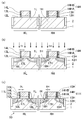
- FIGS. 1A to 1C are diagrams schematically illustrating an exemplary semiconductor device and a manufacturing method thereof according to the first embodiment of the present disclosure.
- 2A to 2C are diagrams schematically illustrating an exemplary semiconductor device and a manufacturing method thereof according to the first embodiment of the present disclosure following FIG. 1C.
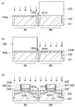
- 3A to 3C are diagrams schematically illustrating an exemplary semiconductor device and a manufacturing method thereof according to the second embodiment of the present disclosure.
- 4A to 4C are diagrams schematically illustrating an exemplary semiconductor device and a manufacturing method thereof according to the first embodiment of the present disclosure following FIG. 3C.
- 5 (a) to 5 (c) are diagrams showing a method for manufacturing a semiconductor device according to the background art.
- FIGS. 1A to 1C and FIGS. 2A to 2C are diagrams schematically showing a structure of an exemplary semiconductor device 10 of this embodiment and a manufacturing method thereof.
- the semiconductor device 10 is formed using a substrate 1 which is a semiconductor substrate made of silicon or the like.
- an active region made of the substrate 1 is defined by an element isolation region 2 made of a silicon oxide film formed by, for example, a LOCOS (Local Oxidation of Silicon) method or an STI (Shallow Trench Isolation) method.
- LOCOS Local Oxidation of Silicon
- STI Shallow Trench Isolation
- Lvt transistor region RL in which a field effect transistor having a low threshold voltage (hereinafter referred to as Lvt transistor) is formed, and a field effect transistor having a threshold voltage higher than that of the Lvt transistor (hereinafter referred to as Lvt transistor).
- Lvt transistor a field effect transistor having a low threshold voltage
- Lvt transistor a field effect transistor having a threshold voltage higher than that of the Lvt transistor
- An Hvt transistor region RH in which an Hvt transistor is called is shown.
- an N-type FET is used as the Lvt transistor and the Hvt transistor.
- a gate electrode 13L is formed on the active region 1L surrounded by the element isolation region 2 in the P-type substrate 1 via a gate insulating film 12L.
- a side wall spacer 15L is formed on the side wall of the gate electrode 13L via an offset spacer 14L.
- N-type source / drain regions 16L (the source region and the drain region are collectively referred to in this way) are formed on both sides of the gate electrode 13L in the active region 1L (outside of the sidewall spacer 15L).
- N-type extension regions 17L are formed on both sides of the channel formation region below the gate electrode 13L in the active region 1L, inside the source / drain region 16L (on the gate electrode 13L side).
- the extension region 17L extends partly from both sides of the gate electrode 13L to below the gate electrode 13L. Between the extension region 17L and the substrate 1, a P-type halo region 18L having a conductivity type different from that of the extension region 17L is formed. The halo region 18L is formed so as to cover the bottom surface and the side surface (excluding the side surface connected to the source / drain region 16L) of the extension region 17L.
- the gate structure 11L of the Lvt transistor is configured by the gate insulating film 12L, the gate electrode 13L, the offset spacer 14L, and the sidewall spacer 15L.
- an Hvt transistor having a structure similar to the Lvt transistor in the Lvt transistor region RL is formed in the Hvt transistor region RH.
- the gate electrode 13H is formed on the active region 1H surrounded by the element isolation region 2 in the P-type substrate 1 via the gate insulating film 12H.
- a side wall spacer 15H is formed on the side wall of the gate electrode 13H via an offset spacer 14H.
- N-type source / drain regions 16H are formed on both sides of the gate electrode 13H in the active region 1H, and an N-type extension region 17H extending partially below the gate electrode 13H is formed on the inside thereof. Yes.
- a P-type halo region 18H having a conductivity type different from that of the extension region 17H is formed between the extension region 17H and the substrate 1.
- the halo region 18H is formed so as to cover the bottom surface and the side surface (excluding the side surface connected to the source / drain region 16H) of the extension region 17H.
- the gate structure 11H of the Hvt transistor is configured by the gate insulating film 12H, the gate electrode 13H, the offset spacer 14H, and the sidewall spacer 15H.
- the offset spacer 14H in the Hvt transistor has a two-layered structure including a first layer 14HA having an L-shaped cross-section in contact with the side wall of the gate electrode 13H and a second layer 14HB stacked on the first layer 14HA. It is a structure, and the combined thickness of the two layers is thicker than the single-layer offset spacer 14L in the Lvt transistor.
- the length of the extension region 17L (the amount of overlap with the gate electrode 13L) of the portion extending below the gate electrode 13L in the Lvt transistor is DL, and the portion of the Hvt transistor extending below the gate electrode 13H is DL. If the length of the extension region 17H is DH, DL is longer than DH. In other words, the length DL where the gate electrode 13L and the extension region 17L overlap is longer than the length DH where the gate electrode 13H and the extension region 17H overlap.
- the extension region 17L in the Lvt transistor extends further to the inside of the gate electrode than the extension region 17H in the Hvt transistor.
- the dimension in the gate length direction of the gate electrode 13L and the dimension in the gate length direction of the gate electrode 13H are substantially the same dimension. “Substantially the same dimension” means that the design dimensions are the same, and variations occurring in the manufacturing process are included.
- the distance (effective gate length) between the extension regions 17L below the gate electrode 13L of the Lvt transistor is shorter than the distance between the extension regions 17H below the gate electrode 13H of the Hvt transistor.
- the threshold voltage of the Lvt transistor is lower than the threshold voltage of the Hvt transistor.
- the difference between the overlap amount DL and the overlap amount DH is realized by the difference between the thickness of the offset spacer 14L and the thickness of the offset spacer 14H.
- the Lvt transistor formed in the Lvt transistor region RL is a transistor in which high-speed operation is more important than reduction of off-leakage current (GIDL, BTBT, etc. can be ignored). Therefore, the offset spacer 14L is set thin and the threshold voltage is low so that the overlap amount DL is sufficiently long.
- the Hvt transistor formed in the Hvt transistor region RH is a transistor that emphasizes reduction of off-leakage current as compared with the Lvt transistor (GIDL, BTBT, etc. cannot be ignored). Therefore, in order to shorten the overlap amount DH (compared to the overlap amount DL), the offset spacer 14H is set thicker than the offset spacer 14L. However, the extension region 17H is not offset with respect to the gate electrode 13H (the arrangement is such that it does not enter below the gate electrode 13H).
- the amount of overlap between the extension region and the gate electrode can be determined, and the threshold voltage of each transistor can be set.
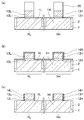
- FIG. 1 (a) shows a state where the gate electrode is formed.
- a P-type substrate 1 which is a semiconductor substrate made of P-type single crystal silicon, a semiconductor substrate made of single-crystal silicon in which a P-type well region is formed, and the like, for example, B (boron) ions which are P-type impurities, etc. Inject. This is performed under predetermined conditions for injecting into the channel formation region on the surface of the substrate 1. Thereafter, a P-type channel diffusion layer is formed by heat treatment (not shown).
- an Lvt transistor region RL for forming a field effect transistor with a low threshold voltage and an Hvt transistor region RH for forming a field effect transistor with a high threshold voltage are determined, and the channel formation region of the substrate 1 is locally Expose.
- an element isolation region 2 is formed on the surface of the substrate 1 by the LOCOS method, the STI method, or the like. Thereby, an active region 1L and an active region 1H made of the substrate 1 surrounded by the element isolation region 2 are formed.
- an insulating film to be the gate insulating films 12L and 12H is formed so as to cover the substrate 1, and an electrode material layer to be the gate electrodes 13L and 13H is further formed thereon.
- the insulating film can be a single layer film or a laminated film of SiO 2 , SiON, HfSiO, HfSiON, HfO 2 or the like.
- a thermal oxidation method a physical vapor deposition method (hereinafter referred to as a PVD (Physical Vapor Deposition) method), a chemical vapor deposition method (hereinafter referred to as a CVD (Chemical Vapor Deposition) method), or the like is used. be able to.
- the electrode material layer may be a single layer structure of a metal material such as Ta, TaN, Ti, TiN, Al, TiAl, or a laminated structure thereof.
- a laminated structure of a metal layer made of any of the aforementioned metal materials and a Si layer formed on the metal layer or a Si-containing layer made of a material containing Si may be used.
- a PVD method, a CVD method, a sputtering method, or the like can be used.
- the resist 20 is formed by patterning so as to correspond to the formation positions of the gate electrode 13L in the Lvt transistor region RL and the gate electrode 13H in the Hvt transistor region RH. Subsequently, the electrode material layer and the insulating film are etched using the resist 20 as a mask to form the gate insulating film 12L and the gate electrode 13L on the active region 1L in the Lvt transistor region RL, while the active in the Hvt transistor region RH. A gate insulating film 12H and a gate electrode 13H are formed on the region 1H. Thereafter, the resist 20 is removed.
- an insulating film serving as an offset spacer is formed on the entire surface of the substrate 1 so as to cover the upper surfaces and side surfaces of the gate electrodes 13L and 13H.
- an insulating film 14A made of SiN is deposited to a thickness of 2 nm to 10 nm
- an insulating film 14B made of an SiO 2 film is deposited to a thickness of 2 nm to 10 nm so as to cover the insulating film 14A.
- a CVD method or the like may be used as a formation method.
- the insulating film 14A is an SiN film and the insulating film 14B is an SiO 2 film, but these materials may be reversed. In addition, other materials can be used as long as the insulating film 14B can be selectively removed with respect to the insulating film 14A.
- a resist material is applied to the entire surface of the substrate 1 and then patterned so that only the Hvt transistor region RH is masked to form a resist 21. Thereafter, wet etching is performed using the resist 21 as a mask, and only the insulating film 14B in the Lvt transistor region RL is selectively removed. Thereafter, the resist 21 is removed. As a result, the insulating film 14B on the active region 1L is removed and only the insulating film 14A remains, and both the insulating film 14A and the insulating film 14B remain on the active region 1H.
- an offset spacer 14L having a single layer structure is formed from the insulating film 14A on the side of the gate electrode 13L in the Lvt transistor region RL. Further, on the side of the gate electrode 13H in the Hvt transistor region RH, a first layer 14HA having an L-shaped cross-sectional shape made of an insulating film 14A and a second layer 14HB formed on the first layer 14HA are formed. An offset spacer 14H having a two-layer structure is formed.
- the offset spacer 14H in the Hvt transistor region RH has a structure in which the second layer 14HB is laminated on the first layer 14HA made of the same insulating film 14A as the offset spacer 14L in the Lvt transistor region RL. The thickness is increased by the thickness of the two layers 14HB.
- extension regions and halo regions are formed.
- ions of As or P which are N-type impurities are implanted.
- the implantation conditions for example, when the implanted ion is As, the implantation energy is 2 keV, the dose is 1 to 2 ⁇ 10 15 / cm 2 , and the implantation angle is 0 ° (with respect to the normal of the main surface of the substrate 1). The angle formed is 0 °).
- the gate electrode 13L and the offset spacer 14L serve as a mask so that the N-type extension region 17L overlaps the active region 1L below the gate electrode 13L by the overlap amount DL. Formed.
- the gate electrode 13H and the offset spacer 14H thicker than the offset spacer 14L in the Lvt transistor region RL serve as a mask, and the N-type extension region 17H is formed in the active region 1H. It is formed to overlap with the overlap amount DH below 13H.
- the offset spacer 14L is thinner than the offset spacer 14H, even if extension implantation is similarly performed on the Lvt transistor region RL and the Hvt transistor region RH, the overlap amount DL is larger than the overlap amount DH. become longer. Therefore, it is not necessary to separately perform extension implantation for the Lvt transistor region RL and the Hvt transistor region RH for the purpose of providing a difference in effective gate length. Therefore, a plurality of field effect transistors having different threshold voltages can be provided on the same substrate without increasing the mask process.
- P-type halo regions 18L and 18H are formed so as to cover the lower portions of the extension regions 17L and 17H, respectively, and be positioned between the substrate 1 and the P-type halo regions 18L and 18H.
- B, BF 2 or In is ion-implanted as a P-type impurity.
- the implantation conditions for example, when the implanted ion is B, the implantation energy is 5 to 10 keV, the dose is 1 to 4 ⁇ 10 13 / cm 2 , and the implantation angle is 15 to 38 °.
- the difference in threshold voltage between the Lvt transistor having a low threshold voltage and the Hvt transistor having a high threshold voltage is an effective gate length (distance between the extension regions below the gate electrode) of the Lvt transistor and the Hvt transistor. Realized by differences. Since the effective gate length difference is determined by the difference between the overlap amounts DL and DH, the difference in the thickness of the offset spacer is set in accordance with the required difference in gate length.
- the difference in threshold voltage between the Lvt transistor having a low threshold voltage and the Hvt transistor having a high threshold voltage is preferably about 50 to 100 mV, for example.
- the threshold voltage varies by 100 mV.
- the thickness of the offset spacer is also set to a difference of 2 nm to 4 nm (4 nm to 8 nm in total) on both sides of the gate electrode so that a difference of 4 nm to 8 nm appears in the effective gate length. That is, the offset spacer 14H in the Hvt transistor region RH is set to be 2 nm to 4 nm thicker than the offset spacer 14L in the Lvt transistor region RL. In other words, the film thickness of the second layer 14HB in the offset spacer 14H may be 2 nm to 4 nm.
- the overlap amount DH becomes 2 nm to 4 nm (more than the overlap amount DL) on both sides of the gate electrode 13H, and the effective gate length difference can be 4 nm to 8 nm.
- the above numerical value is a desirable example when the gate length direction of the gate electrodes 13L and 13H itself is about 40 nm, but is not limited thereto. It can be set based on the dimensions of the gate electrode, the concentration of various impurity regions (extension regions, source / drain regions, etc.), the desired threshold voltage difference, and the like.
- an insulating film made of a single layer film of SiO 2 film, SiN film or SiON film, or a laminated film thereof is formed on the substrate 1 so as to cover the gate electrode 13L, the gate electrode 13H, and the like.
- anisotropic dry etching is performed on the insulating film, and other portions are removed except for the lateral portions of the gate electrode 13L and the gate electrode 13H.
- the side wall spacer 15L is formed on the side of the gate electrode 13L via the offset spacer 14L, while the side wall spacer 15H is formed on the side of the gate electrode 13H via the offset spacer 14H.
- the distance between the gate electrode 13L and the side wall spacer 15L is shorter than the distance between the gate electrode 13H and the side wall spacer 15H.
- the gate structure 11L is formed in the Lvt transistor region RL, and the gate structure 11H is formed in the Hvt transistor region RH.
- N-type impurities such as As are ion-implanted into the active region 1L and the active region 1H, thereby forming N-type on both sides of the gate structure 11L and the gate structure 11H, respectively.
- Source / drain regions 16L and 16H are formed.
- the semiconductor device 10 including the Lvt transistor and the Hvt transistor is formed on the same substrate. According to such a manufacturing method, field effect transistors having different threshold voltages can be formed without increasing the mask process, and the manufacturing process can be shortened.
- the offset spacer 14H thicker than the offset spacer 14L having a single-layer structure by using a two-layer structure
- a difference in thickness may be provided by other methods.
- the offset spacer 14L may also be provided with an offset spacer 14H having a larger number of layers as a structure having a plurality of layers.
- an Mvt transistor having an intermediate threshold voltage may be provided in addition to the Lvt transistor and the Hvt transistor.
- an offset spacer having an intermediate thickness between the offset spacer 14L and the offset spacer 14H is provided in this case.
- the present invention can be applied to the case where an SRAM transistor or the like is provided.
- FIGS. 3A to 3C and FIGS. 4A to 4C are views schematically showing the structure of the exemplary semiconductor device 10a of the present embodiment and the manufacturing method thereof.
- the same reference numerals as those in FIG. 2C are used for the same components as those of the semiconductor device 10 of the first embodiment, and the differences will be described in detail below.
- a gate electrode 13L is formed on the active region 1L surrounded by the element isolation region 2 in the P-type substrate 1 via a gate insulating film 12L.
- a side wall spacer 15L is formed on the side of the gate electrode 13L in contact with the side wall of the gate electrode 13L without using an offset spacer.
- the gate structure 11L of the Lvt transistor region RL is configured by the gate insulating film 12L, the gate electrode 13L, and the sidewall spacer 15L.
- an N-type extension region 17L is formed so as to overlap with the overlap amount DL below the gate electrode 13L.
- An N-type source / drain region 16L is formed outside the extension region 17L, and a P-type halo region 18L is formed between the extension region 17L and the substrate 1 so as to cover the lower side of the extension region 17L. Has been.
- a gate electrode 13H is formed on the active region 1H surrounded by the element isolation region 2 in the P-type substrate 1 via the gate insulating film 12H.
- a side wall spacer 15H is formed on the side of the gate electrode 13H via an offset spacer 14H.
- the gate structure 11H of the Hvt transistor region RH is configured by the gate insulating film 12H, the gate electrode 13H, the offset spacer 14H, and the sidewall spacer 15H.
- an N-type extension region 17H is formed so as to overlap with the overlap amount DH below the gate electrode 13H.
- An N-type source / drain region 16H is formed outside the extension region 17H, and a P-type halo region 18H is formed between the extension region 17H and the substrate 1 so as to cover the extension region 17H. Has been.
- the overlap amount DL in the Lvt transistor is longer than the overlap amount DH in the Hvt transistor.
- the distance (effective gate length) between the extension regions 17L below the gate electrode 13L of the Lvt transistor is shorter than the distance between the extension regions 17H below the gate electrode 13H of the Hvt transistor.
- the threshold voltage of the Lvt transistor is lower than the threshold voltage of the Hvt transistor.
- the difference between the overlap amount DL and the overlap amount DL is realized by not providing the offset spacer in the Lvt transistor and providing the offset spacer 14H in the Hvt transistor.
- FIG. 3 (a) shows a state where the gate electrode is formed. This may be formed in the same manner as described with reference to FIG. 1A in the first embodiment. After obtaining the configuration of FIG. 3A, the resist 20 is removed.
- an insulating film 14A serving as an offset spacer is formed so as to cover the upper surface and side surfaces of the gate electrode 13L and the gate electrode 13H.
- a SiN film, a SiO 2 film, or the like is used and formed to a thickness of 2 nm to 10 nm by a CVD method.
- anisotropic etching is performed on the entire surface of the substrate 1 to etch back the entire surface of the insulating film 14A, leaving only the portions covering the side walls of the gate electrodes and other portions.
- an offset spacer is formed. More specifically, an offset spacer 14H that covers the side wall of the gate electrode 13H in the Hvt transistor region RH is formed. Also in the Lvt transistor region RL, an offset spacer 14L that covers the side wall of the gate electrode 13L is formed.
- the offset spacer 14L in the Lvt transistor region RL is removed.
- resist is applied and patterned as a resist 21 covering only the Hvt transistor region RH.
- Wet etching is performed using the resist 21 as a mask, and the offset spacer 14L in the Lvt transistor region RL is selectively removed. Thereafter, the resist 21 is removed.
- an N-type extension region and a P-type halo region are formed.
- As or P that is an N-type impurity is ion-implanted under the same conditions as described in the first embodiment.
- the extension region 17L is formed in the active region 1L.
- the extension region 17L is formed to overlap with the overlap amount DL below the gate electrode 13L.
- the gate electrode 13H and the offset spacer 14H serve as a mask.
- the extension region 17H is formed to overlap the overlap amount DH below the gate electrode 13H.
- the offset spacer 14H is formed only in the Hvt transistor region RH, the overlap amount DL is longer than the overlap amount DH even if extension implantation is similarly performed on the Lvt transistor region RL and the Hvt transistor region RH. Become. Therefore, it is possible to provide a difference in effective gate length between the Lvt transistor and the Hvt transistor without requiring a separate mask process and implantation process, and a plurality of field effect transistors having different threshold voltages can be formed on the same substrate. Can be provided.
- the halo regions 18L and 18H are formed so as to cover the lower portions of the extension regions 17L and 17H, respectively, and to be positioned between the substrate 1 and the substrate.
- B, BF 2 or In is ion-implanted as a P-type impurity.
- the injection conditions may be the same as those in the first embodiment.
- the thickness of the offset spacer 14H in the Hvt transistor region RH is set in accordance with a necessary difference in gate length.
- the desired threshold voltage difference between the Lvt transistor and the Hvt transistor is about 50 to 100 mV. Further, it is assumed that the threshold voltage fluctuates by 100 mV with respect to an effective gate length fluctuation of 8 nm. In such a case, the effective gate length difference between the Lvt transistor and the Hvt transistor may be 4 nm to 8 nm. Therefore, the thickness of the offset spacer 14H may be formed to 2 nm to 4 nm.
- the overlap amount DH is increased by 2 nm to 4 nm on both sides of the gate electrode 13H (more than the overlap amount DL), and the effective gate length difference can be 4 nm to 8 nm.
- these numerical values are merely examples, and can be set based on the dimensions of the gate electrode, the concentrations of various impurity regions, the desired threshold voltage difference, and the like.
- an insulating film is formed on the substrate 1 so as to cover the gate electrode 13L, the gate electrode 13H, and the like, and anisotropic dry etching is performed on the insulating film to thereby form a sidewall spacer in contact with the side surface of the gate electrode 13L.
- 15L and a sidewall spacer 15H formed on the side of the gate electrode 13H via an offset spacer 14H are obtained.
- the gate structure 11L is formed in the Lvt transistor region RL, and the gate structure 11H is formed in the Hvt transistor region RH.
- N-type impurities such as As are ion-implanted into the active region 1L and the active region 1H, thereby forming N-type on both sides of the gate structure 11L and the gate structure 11H, respectively.
- Source / drain regions 16L and 16H are formed.
- the semiconductor device 10a is formed. According to such a manufacturing method, field effect transistors having different threshold voltages can be formed without increasing the mask process, and the manufacturing process can be shortened.
- the overlap amount between the gate electrode and the extension region can be set to three or more by one extension injection.
- each of the first and second embodiments an N-channel transistor has been described as an example. However, each configuration can be applied to a P-channel transistor.
- channel injection may be performed separately for the Lvt transistor and the Hvt transistor. As a result, the number of steps related to channel implantation increases, but the controllability of the threshold voltage can be further improved.
- the technology of the present disclosure it is possible to realize a semiconductor device including a plurality of field effect transistors having different threshold voltages and a method for manufacturing the same while suppressing an increase in manufacturing steps, and also for miniaturization of a semiconductor device. It is possible.
Abstract
La présente invention a trait à un dispositif à semi-conducteur qui comprend un premier transistor à effet de champ et un second transistor à effet de champ du même type de conduction. Le premier transistor à effet de champ est équipé d'une première électrode de grille (13L) sur un substrat (1), d'une première paroi latérale (15L) sur son côté, d'une première zone d'extension (17L) d'une première zone active (1L) des deux côtés de la première électrode de grille (13L). Le second transistor à effet de champ est équipé d'une seconde électrode de grille (13H) sur le substrat (1), d'une seconde paroi latérale (15H) sur son côté, d'une seconde zone d'extension (17H) d'une seconde zone active (1H) des deux côtés de la seconde électrode de grille (13H). Dans la direction de la longueur de la grille, le chevauchement entre la première zone d'extension (17L) et la première électrode de grille (13L) est supérieur au chevauchement entre la seconde zone d'extension (17H) et la seconde électrode de grille (13H). La distance entre la première électrode de grille (13L) et la première paroi latérale (15L) est inférieure à la distance entre la seconde électrode de grille (13H) et la seconde paroi latérale (15H).
Priority Applications (1)
| Application Number | Priority Date | Filing Date | Title |
|---|---|---|---|
| US13/399,004 US20120161245A1 (en) | 2009-12-21 | 2012-02-17 | Semiconductor device and method for fabricating the same |
Applications Claiming Priority (2)
| Application Number | Priority Date | Filing Date | Title |
|---|---|---|---|
| JP2009-289041 | 2009-12-21 | ||
| JP2009289041A JP5435720B2 (ja) | 2009-12-21 | 2009-12-21 | 半導体装置 |
Related Child Applications (1)
| Application Number | Title | Priority Date | Filing Date |
|---|---|---|---|
| US13/399,004 Continuation US20120161245A1 (en) | 2009-12-21 | 2012-02-17 | Semiconductor device and method for fabricating the same |
Publications (1)
| Publication Number | Publication Date |
|---|---|
| WO2011077606A1 true WO2011077606A1 (fr) | 2011-06-30 |
Family
ID=44195160
Family Applications (1)
| Application Number | Title | Priority Date | Filing Date |
|---|---|---|---|
| PCT/JP2010/004887 WO2011077606A1 (fr) | 2009-12-21 | 2010-08-03 | Dispositif à semi-conducteur et procédé de fabrication associé |
Country Status (3)
| Country | Link |
|---|---|
| US (1) | US20120161245A1 (fr) |
| JP (1) | JP5435720B2 (fr) |
| WO (1) | WO2011077606A1 (fr) |
Families Citing this family (5)
| Publication number | Priority date | Publication date | Assignee | Title |
|---|---|---|---|---|
| JP5847537B2 (ja) * | 2011-10-28 | 2016-01-27 | ルネサスエレクトロニクス株式会社 | 半導体装置の製造方法および半導体装置 |
| US8822295B2 (en) * | 2012-04-03 | 2014-09-02 | International Business Machines Corporation | Low extension dose implants in SRAM fabrication |
| JP5927017B2 (ja) * | 2012-04-20 | 2016-05-25 | ルネサスエレクトロニクス株式会社 | 半導体装置及び半導体装置の製造方法 |
| JP6275559B2 (ja) * | 2014-06-13 | 2018-02-07 | ルネサスエレクトロニクス株式会社 | 半導体装置およびその製造方法 |
| US20190081044A1 (en) * | 2016-04-01 | 2019-03-14 | Intel Corporation | Semiconductor device having sub regions to define threshold voltages |
Citations (7)
| Publication number | Priority date | Publication date | Assignee | Title |
|---|---|---|---|---|
| JPH08107157A (ja) * | 1994-10-06 | 1996-04-23 | Toshiba Microelectron Corp | 半導体装置とその製造方法 |
| JPH09283760A (ja) * | 1995-12-29 | 1997-10-31 | Lg Semicon Co Ltd | 半導体素子の製造方法 |
| JP2001196475A (ja) * | 2000-01-12 | 2001-07-19 | Matsushita Electric Ind Co Ltd | 半導体装置及びその製造方法 |
| JP2002026139A (ja) * | 2000-06-30 | 2002-01-25 | Toshiba Corp | 半導体装置及び半導体装置の製造方法 |
| JP2002231821A (ja) * | 2001-01-31 | 2002-08-16 | Mitsubishi Electric Corp | 半導体装置の製造方法及び半導体装置 |
| JP2003249568A (ja) * | 2003-01-31 | 2003-09-05 | Oki Electric Ind Co Ltd | 半導体装置の製造方法 |
| JP2005303087A (ja) * | 2004-04-13 | 2005-10-27 | Matsushita Electric Ind Co Ltd | 半導体装置およびその製造方法 |
Family Cites Families (28)
| Publication number | Priority date | Publication date | Assignee | Title |
|---|---|---|---|---|
| JPH1167927A (ja) * | 1997-06-09 | 1999-03-09 | Mitsubishi Electric Corp | 半導体装置およびその製造方法 |
| KR19990030993A (ko) * | 1997-10-08 | 1999-05-06 | 윤종용 | 고속동작을 위한 모스트랜지스터구조 |
| US5989966A (en) * | 1997-12-15 | 1999-11-23 | Taiwan Semiconductor Manufacturing Company, Ltd. | Method and a deep sub-micron field effect transistor structure for suppressing short channel effects |
| US6124610A (en) * | 1998-06-26 | 2000-09-26 | Advanced Micro Devices, Inc. | Isotropically etching sidewall spacers to be used for both an NMOS source/drain implant and a PMOS LDD implant |
| JP2000150885A (ja) * | 1998-09-07 | 2000-05-30 | Seiko Epson Corp | Mosトランジスタの閾値電圧設定方法および半導体装置 |
| JP4481388B2 (ja) * | 1999-06-25 | 2010-06-16 | 独立行政法人情報通信研究機構 | 絶縁ゲート型電界効果トランジスタおよびその製造方法 |
| JP2001015704A (ja) | 1999-06-29 | 2001-01-19 | Hitachi Ltd | 半導体集積回路 |
| JP3275896B2 (ja) * | 1999-10-06 | 2002-04-22 | 日本電気株式会社 | 半導体装置の製造方法 |
| JP4635333B2 (ja) * | 2000-12-14 | 2011-02-23 | ソニー株式会社 | 半導体装置の製造方法 |
| JP2003197765A (ja) * | 2001-12-28 | 2003-07-11 | Texas Instr Japan Ltd | 半導体装置およびその製造方法 |
| US6849492B2 (en) * | 2002-07-08 | 2005-02-01 | Micron Technology, Inc. | Method for forming standard voltage threshold and low voltage threshold MOSFET devices |
| JP4393109B2 (ja) * | 2003-05-21 | 2010-01-06 | 株式会社ルネサステクノロジ | 半導体装置の製造方法 |
| US7064396B2 (en) * | 2004-03-01 | 2006-06-20 | Freescale Semiconductor, Inc. | Integrated circuit with multiple spacer insulating region widths |
| KR100827443B1 (ko) * | 2006-10-11 | 2008-05-06 | 삼성전자주식회사 | 손상되지 않은 액티브 영역을 가진 반도체 소자 및 그 제조방법 |
| US7456066B2 (en) * | 2006-11-03 | 2008-11-25 | Taiwan Semiconductor Manufacturing Co., Ltd. | Variable width offset spacers for mixed signal and system on chip devices |
| JP4320405B2 (ja) * | 2007-03-27 | 2009-08-26 | Okiセミコンダクタ株式会社 | 半導体装置及びその製造方法 |
| US7718496B2 (en) * | 2007-10-30 | 2010-05-18 | International Business Machines Corporation | Techniques for enabling multiple Vt devices using high-K metal gate stacks |
| JP2009141168A (ja) * | 2007-12-07 | 2009-06-25 | Panasonic Corp | 半導体装置及びその製造方法 |
| JP2009277771A (ja) * | 2008-05-13 | 2009-11-26 | Panasonic Corp | 半導体装置とその製造方法 |
| US7951678B2 (en) * | 2008-08-12 | 2011-05-31 | International Business Machines Corporation | Metal-gate high-k reference structure |
| JP2010123669A (ja) * | 2008-11-18 | 2010-06-03 | Nec Electronics Corp | 半導体装置およびその製造方法 |
| JP2010153683A (ja) * | 2008-12-26 | 2010-07-08 | Hitachi Ltd | 半導体装置 |
| US8106455B2 (en) * | 2009-04-30 | 2012-01-31 | International Business Machines Corporation | Threshold voltage adjustment through gate dielectric stack modification |
| DE102009021486B4 (de) * | 2009-05-15 | 2013-07-04 | Globalfoundries Dresden Module One Llc & Co. Kg | Verfahren zur Feldeffekttransistor-Herstellung |
| US20100308418A1 (en) * | 2009-06-09 | 2010-12-09 | Knut Stahrenberg | Semiconductor Devices and Methods of Manufacture Thereof |
| US8105892B2 (en) * | 2009-08-18 | 2012-01-31 | International Business Machines Corporation | Thermal dual gate oxide device integration |
| US8283734B2 (en) * | 2010-04-09 | 2012-10-09 | Taiwan Semiconductor Manufacturing Company, Ltd. | Multi-threshold voltage device and method of making same |
| DE102010063781B4 (de) * | 2010-12-21 | 2016-08-11 | Globalfoundries Dresden Module One Limited Liability Company & Co. Kg | Unterschiedliche Schwellwertspannungseinstellung in PMOS-Transistoren durch unterschiedliche Herstellung eines Kanalhalbleitermaterials |
-
2009
- 2009-12-21 JP JP2009289041A patent/JP5435720B2/ja not_active Expired - Fee Related
-
2010
- 2010-08-03 WO PCT/JP2010/004887 patent/WO2011077606A1/fr active Application Filing
-
2012
- 2012-02-17 US US13/399,004 patent/US20120161245A1/en not_active Abandoned
Patent Citations (7)
| Publication number | Priority date | Publication date | Assignee | Title |
|---|---|---|---|---|
| JPH08107157A (ja) * | 1994-10-06 | 1996-04-23 | Toshiba Microelectron Corp | 半導体装置とその製造方法 |
| JPH09283760A (ja) * | 1995-12-29 | 1997-10-31 | Lg Semicon Co Ltd | 半導体素子の製造方法 |
| JP2001196475A (ja) * | 2000-01-12 | 2001-07-19 | Matsushita Electric Ind Co Ltd | 半導体装置及びその製造方法 |
| JP2002026139A (ja) * | 2000-06-30 | 2002-01-25 | Toshiba Corp | 半導体装置及び半導体装置の製造方法 |
| JP2002231821A (ja) * | 2001-01-31 | 2002-08-16 | Mitsubishi Electric Corp | 半導体装置の製造方法及び半導体装置 |
| JP2003249568A (ja) * | 2003-01-31 | 2003-09-05 | Oki Electric Ind Co Ltd | 半導体装置の製造方法 |
| JP2005303087A (ja) * | 2004-04-13 | 2005-10-27 | Matsushita Electric Ind Co Ltd | 半導体装置およびその製造方法 |
Also Published As
| Publication number | Publication date |
|---|---|
| JP2011129811A (ja) | 2011-06-30 |
| JP5435720B2 (ja) | 2014-03-05 |
| US20120161245A1 (en) | 2012-06-28 |
Similar Documents
| Publication | Publication Date | Title |
|---|---|---|
| US7732839B2 (en) | Semiconductor device and method for fabricating the same | |
| JP4850174B2 (ja) | 半導体装置及びその製造方法 | |
| KR102008738B1 (ko) | 반도체 장치 및 그 제조 방법 | |
| TWI485854B (zh) | 於三維電晶體中基於應變隔離材料之應變工程 | |
| US9245975B2 (en) | Recessed channel insulated-gate field effect transistor with self-aligned gate and increased channel length | |
| US9966456B1 (en) | Methods of forming gate electrodes on a vertical transistor device | |
| TWI714583B (zh) | 半導體裝置及其形成方法 | |
| JP2012164699A (ja) | 半導体装置 | |
| JP5627165B2 (ja) | 半導体装置及び半導体装置の製造方法 | |
| JP5435720B2 (ja) | 半導体装置 | |
| KR101033700B1 (ko) | 동일 기판 상에 도전 타입이 같은 로우 및 하이 퍼포먼스장치를 갖는 반도체 장치 구조 | |
| JP5137378B2 (ja) | 半導体装置及びその製造方法 | |
| KR20100138973A (ko) | 높이가 감소된 금속 게이트 스택을 포함하는 반도체 디바이스 및 상기 반도체 디바이스를 제조하는 방법 | |
| US7723777B2 (en) | Semiconductor device and method for making same | |
| JP5064289B2 (ja) | 半導体装置およびその製造方法 | |
| TW202129964A (zh) | 先進邏輯操作的電荷捕捉tfet半導體元件製作方法 | |
| JP5444176B2 (ja) | 半導体装置 | |
| KR100488540B1 (ko) | 반도체소자 및 이를 제조하는 방법 | |
| JP2014123668A (ja) | Mos型半導体装置及びその製造方法 | |
| JP2000200836A (ja) | 半導体装置およびその製造方法 | |
| US8329526B2 (en) | Cap removal in a high-k metal gate electrode structure by using a sacrificial fill material | |
| JP4630235B2 (ja) | 半導体装置及びその製造方法 | |
| JP5073158B2 (ja) | 半導体装置及びその製造方法 | |
| KR100762895B1 (ko) | 리세스 게이트를 갖는 반도체 소자의 제조방법 | |
| JP2012043861A (ja) | 半導体装置の製造方法 |
Legal Events
| Date | Code | Title | Description |
|---|---|---|---|
| 121 | Ep: the epo has been informed by wipo that ep was designated in this application |
Ref document number: 10838847 Country of ref document: EP Kind code of ref document: A1 |
|
| NENP | Non-entry into the national phase |
Ref country code: DE |
|
| 122 | Ep: pct application non-entry in european phase |
Ref document number: 10838847 Country of ref document: EP Kind code of ref document: A1 |