WO2011024790A1 - 樹脂多層基板及び該樹脂多層基板の製造方法 - Google Patents
樹脂多層基板及び該樹脂多層基板の製造方法 Download PDFInfo
- Publication number
- WO2011024790A1 WO2011024790A1 PCT/JP2010/064253 JP2010064253W WO2011024790A1 WO 2011024790 A1 WO2011024790 A1 WO 2011024790A1 JP 2010064253 W JP2010064253 W JP 2010064253W WO 2011024790 A1 WO2011024790 A1 WO 2011024790A1
- Authority
- WO
- WIPO (PCT)
- Prior art keywords
- resin layer
- via hole
- resin
- layer
- multilayer substrate
- Prior art date
- Legal status (The legal status is an assumption and is not a legal conclusion. Google has not performed a legal analysis and makes no representation as to the accuracy of the status listed.)
- Ceased
Links
Images







Classifications
-
- H—ELECTRICITY
- H05—ELECTRIC TECHNIQUES NOT OTHERWISE PROVIDED FOR
- H05K—PRINTED CIRCUITS; CASINGS OR CONSTRUCTIONAL DETAILS OF ELECTRIC APPARATUS; MANUFACTURE OF ASSEMBLAGES OF ELECTRICAL COMPONENTS
- H05K3/00—Apparatus or processes for manufacturing printed circuits
- H05K3/46—Manufacturing multilayer circuits
-
- H—ELECTRICITY
- H10—SEMICONDUCTOR DEVICES; ELECTRIC SOLID-STATE DEVICES NOT OTHERWISE PROVIDED FOR
- H10W—GENERIC PACKAGES, INTERCONNECTIONS, CONNECTORS OR OTHER CONSTRUCTIONAL DETAILS OF DEVICES COVERED BY CLASS H10
- H10W70/00—Package substrates; Interposers; Redistribution layers [RDL]
- H10W70/60—Insulating or insulated package substrates; Interposers; Redistribution layers
- H10W70/611—Insulating or insulated package substrates; Interposers; Redistribution layers for connecting multiple chips together
- H10W70/614—Insulating or insulated package substrates; Interposers; Redistribution layers for connecting multiple chips together the multiple chips being integrally enclosed
-
- H—ELECTRICITY
- H05—ELECTRIC TECHNIQUES NOT OTHERWISE PROVIDED FOR
- H05K—PRINTED CIRCUITS; CASINGS OR CONSTRUCTIONAL DETAILS OF ELECTRIC APPARATUS; MANUFACTURE OF ASSEMBLAGES OF ELECTRICAL COMPONENTS
- H05K1/00—Printed circuits
- H05K1/02—Details
- H05K1/11—Printed elements for providing electric connections to or between printed circuits
-
- H—ELECTRICITY
- H05—ELECTRIC TECHNIQUES NOT OTHERWISE PROVIDED FOR
- H05K—PRINTED CIRCUITS; CASINGS OR CONSTRUCTIONAL DETAILS OF ELECTRIC APPARATUS; MANUFACTURE OF ASSEMBLAGES OF ELECTRICAL COMPONENTS
- H05K1/00—Printed circuits
- H05K1/18—Printed circuits structurally associated with non-printed electric components
- H05K1/182—Printed circuits structurally associated with non-printed electric components associated with components mounted in printed circuit boards [PCB], e.g. insert-mounted components [IMC]
- H05K1/185—Printed circuits structurally associated with non-printed electric components associated with components mounted in printed circuit boards [PCB], e.g. insert-mounted components [IMC] associated with components encapsulated in the insulating substrate of the PCBs; associated with components incorporated in internal layers of multilayer circuit boards
- H05K1/186—Printed circuits structurally associated with non-printed electric components associated with components mounted in printed circuit boards [PCB], e.g. insert-mounted components [IMC] associated with components encapsulated in the insulating substrate of the PCBs; associated with components incorporated in internal layers of multilayer circuit boards manufactured by mounting on or connecting to patterned circuits before or during embedding
-
- H—ELECTRICITY
- H05—ELECTRIC TECHNIQUES NOT OTHERWISE PROVIDED FOR
- H05K—PRINTED CIRCUITS; CASINGS OR CONSTRUCTIONAL DETAILS OF ELECTRIC APPARATUS; MANUFACTURE OF ASSEMBLAGES OF ELECTRICAL COMPONENTS
- H05K3/00—Apparatus or processes for manufacturing printed circuits
- H05K3/40—Forming printed elements for providing electric connections to or between printed circuits
-
- H—ELECTRICITY
- H10—SEMICONDUCTOR DEVICES; ELECTRIC SOLID-STATE DEVICES NOT OTHERWISE PROVIDED FOR
- H10W—GENERIC PACKAGES, INTERCONNECTIONS, CONNECTORS OR OTHER CONSTRUCTIONAL DETAILS OF DEVICES COVERED BY CLASS H10
- H10W70/00—Package substrates; Interposers; Redistribution layers [RDL]
- H10W70/60—Insulating or insulated package substrates; Interposers; Redistribution layers
-
- H—ELECTRICITY
- H10—SEMICONDUCTOR DEVICES; ELECTRIC SOLID-STATE DEVICES NOT OTHERWISE PROVIDED FOR
- H10W—GENERIC PACKAGES, INTERCONNECTIONS, CONNECTORS OR OTHER CONSTRUCTIONAL DETAILS OF DEVICES COVERED BY CLASS H10
- H10W70/00—Package substrates; Interposers; Redistribution layers [RDL]
- H10W70/60—Insulating or insulated package substrates; Interposers; Redistribution layers
- H10W70/62—Insulating or insulated package substrates; Interposers; Redistribution layers characterised by their interconnections
- H10W70/63—Vias, e.g. via plugs
- H10W70/635—Through-vias
-
- H—ELECTRICITY
- H10—SEMICONDUCTOR DEVICES; ELECTRIC SOLID-STATE DEVICES NOT OTHERWISE PROVIDED FOR
- H10W—GENERIC PACKAGES, INTERCONNECTIONS, CONNECTORS OR OTHER CONSTRUCTIONAL DETAILS OF DEVICES COVERED BY CLASS H10
- H10W72/00—Interconnections or connectors in packages
-
- H—ELECTRICITY
- H10—SEMICONDUCTOR DEVICES; ELECTRIC SOLID-STATE DEVICES NOT OTHERWISE PROVIDED FOR
- H10W—GENERIC PACKAGES, INTERCONNECTIONS, CONNECTORS OR OTHER CONSTRUCTIONAL DETAILS OF DEVICES COVERED BY CLASS H10
- H10W90/00—Package configurations
-
- H—ELECTRICITY
- H05—ELECTRIC TECHNIQUES NOT OTHERWISE PROVIDED FOR
- H05K—PRINTED CIRCUITS; CASINGS OR CONSTRUCTIONAL DETAILS OF ELECTRIC APPARATUS; MANUFACTURE OF ASSEMBLAGES OF ELECTRICAL COMPONENTS
- H05K2201/00—Indexing scheme relating to printed circuits covered by H05K1/00
- H05K2201/01—Dielectrics
- H05K2201/0183—Dielectric layers
- H05K2201/0195—Dielectric or adhesive layers comprising a plurality of layers, e.g. in a multilayer structure
-
- H—ELECTRICITY
- H05—ELECTRIC TECHNIQUES NOT OTHERWISE PROVIDED FOR
- H05K—PRINTED CIRCUITS; CASINGS OR CONSTRUCTIONAL DETAILS OF ELECTRIC APPARATUS; MANUFACTURE OF ASSEMBLAGES OF ELECTRICAL COMPONENTS
- H05K2201/00—Indexing scheme relating to printed circuits covered by H05K1/00
- H05K2201/09—Shape and layout
- H05K2201/09209—Shape and layout details of conductors
- H05K2201/09372—Pads and lands
- H05K2201/09481—Via in pad; Pad over filled via
-
- H—ELECTRICITY
- H05—ELECTRIC TECHNIQUES NOT OTHERWISE PROVIDED FOR
- H05K—PRINTED CIRCUITS; CASINGS OR CONSTRUCTIONAL DETAILS OF ELECTRIC APPARATUS; MANUFACTURE OF ASSEMBLAGES OF ELECTRICAL COMPONENTS
- H05K2201/00—Indexing scheme relating to printed circuits covered by H05K1/00
- H05K2201/09—Shape and layout
- H05K2201/09818—Shape or layout details not covered by a single group of H05K2201/09009 - H05K2201/09809
- H05K2201/09827—Tapered, e.g. tapered hole, via or groove
-
- H—ELECTRICITY
- H05—ELECTRIC TECHNIQUES NOT OTHERWISE PROVIDED FOR
- H05K—PRINTED CIRCUITS; CASINGS OR CONSTRUCTIONAL DETAILS OF ELECTRIC APPARATUS; MANUFACTURE OF ASSEMBLAGES OF ELECTRICAL COMPONENTS
- H05K2201/00—Indexing scheme relating to printed circuits covered by H05K1/00
- H05K2201/09—Shape and layout
- H05K2201/09818—Shape or layout details not covered by a single group of H05K2201/09009 - H05K2201/09809
- H05K2201/09845—Stepped hole, via, edge, bump or conductor
-
- H—ELECTRICITY
- H05—ELECTRIC TECHNIQUES NOT OTHERWISE PROVIDED FOR
- H05K—PRINTED CIRCUITS; CASINGS OR CONSTRUCTIONAL DETAILS OF ELECTRIC APPARATUS; MANUFACTURE OF ASSEMBLAGES OF ELECTRICAL COMPONENTS
- H05K2201/00—Indexing scheme relating to printed circuits covered by H05K1/00
- H05K2201/10—Details of components or other objects attached to or integrated in a printed circuit board
- H05K2201/10613—Details of electrical connections of non-printed components, e.g. special leads
- H05K2201/10621—Components characterised by their electrical contacts
- H05K2201/10636—Leadless chip, e.g. chip capacitor or resistor
-
- H—ELECTRICITY
- H05—ELECTRIC TECHNIQUES NOT OTHERWISE PROVIDED FOR
- H05K—PRINTED CIRCUITS; CASINGS OR CONSTRUCTIONAL DETAILS OF ELECTRIC APPARATUS; MANUFACTURE OF ASSEMBLAGES OF ELECTRICAL COMPONENTS
- H05K2203/00—Indexing scheme relating to apparatus or processes for manufacturing printed circuits covered by H05K3/00
- H05K2203/01—Tools for processing; Objects used during processing
- H05K2203/0191—Using tape or non-metallic foil in a process, e.g. during filling of a hole with conductive paste
-
- H—ELECTRICITY
- H05—ELECTRIC TECHNIQUES NOT OTHERWISE PROVIDED FOR
- H05K—PRINTED CIRCUITS; CASINGS OR CONSTRUCTIONAL DETAILS OF ELECTRIC APPARATUS; MANUFACTURE OF ASSEMBLAGES OF ELECTRICAL COMPONENTS
- H05K3/00—Apparatus or processes for manufacturing printed circuits
- H05K3/40—Forming printed elements for providing electric connections to or between printed circuits
- H05K3/4038—Through-connections; Vertical interconnect access [VIA] connections
- H05K3/4053—Through-connections; Vertical interconnect access [VIA] connections by thick-film techniques
- H05K3/4069—Through-connections; Vertical interconnect access [VIA] connections by thick-film techniques for via connections in organic insulating substrates
-
- H—ELECTRICITY
- H05—ELECTRIC TECHNIQUES NOT OTHERWISE PROVIDED FOR
- H05K—PRINTED CIRCUITS; CASINGS OR CONSTRUCTIONAL DETAILS OF ELECTRIC APPARATUS; MANUFACTURE OF ASSEMBLAGES OF ELECTRICAL COMPONENTS
- H05K3/00—Apparatus or processes for manufacturing printed circuits
- H05K3/46—Manufacturing multilayer circuits
- H05K3/4644—Manufacturing multilayer circuits by building the multilayer layer by layer, i.e. build-up multilayer circuits
- H05K3/4652—Adding a circuit layer by laminating a metal foil or a preformed metal foil pattern
-
- H—ELECTRICITY
- H05—ELECTRIC TECHNIQUES NOT OTHERWISE PROVIDED FOR
- H05K—PRINTED CIRCUITS; CASINGS OR CONSTRUCTIONAL DETAILS OF ELECTRIC APPARATUS; MANUFACTURE OF ASSEMBLAGES OF ELECTRICAL COMPONENTS
- H05K3/00—Apparatus or processes for manufacturing printed circuits
- H05K3/46—Manufacturing multilayer circuits
- H05K3/4644—Manufacturing multilayer circuits by building the multilayer layer by layer, i.e. build-up multilayer circuits
- H05K3/4673—Application methods or materials of intermediate insulating layers not specially adapted to any one of the previous methods of adding a circuit layer
-
- H—ELECTRICITY
- H10—SEMICONDUCTOR DEVICES; ELECTRIC SOLID-STATE DEVICES NOT OTHERWISE PROVIDED FOR
- H10W—GENERIC PACKAGES, INTERCONNECTIONS, CONNECTORS OR OTHER CONSTRUCTIONAL DETAILS OF DEVICES COVERED BY CLASS H10
- H10W90/00—Package configurations
- H10W90/701—Package configurations characterised by the relative positions of pads or connectors relative to package parts
- H10W90/721—Package configurations characterised by the relative positions of pads or connectors relative to package parts of bump connectors
- H10W90/724—Package configurations characterised by the relative positions of pads or connectors relative to package parts of bump connectors between a chip and a stacked insulating package substrate, interposer or RDL
-
- Y—GENERAL TAGGING OF NEW TECHNOLOGICAL DEVELOPMENTS; GENERAL TAGGING OF CROSS-SECTIONAL TECHNOLOGIES SPANNING OVER SEVERAL SECTIONS OF THE IPC; TECHNICAL SUBJECTS COVERED BY FORMER USPC CROSS-REFERENCE ART COLLECTIONS [XRACs] AND DIGESTS
- Y02—TECHNOLOGIES OR APPLICATIONS FOR MITIGATION OR ADAPTATION AGAINST CLIMATE CHANGE
- Y02P—CLIMATE CHANGE MITIGATION TECHNOLOGIES IN THE PRODUCTION OR PROCESSING OF GOODS
- Y02P70/00—Climate change mitigation technologies in the production process for final industrial or consumer products
- Y02P70/50—Manufacturing or production processes characterised by the final manufactured product
-
- Y—GENERAL TAGGING OF NEW TECHNOLOGICAL DEVELOPMENTS; GENERAL TAGGING OF CROSS-SECTIONAL TECHNOLOGIES SPANNING OVER SEVERAL SECTIONS OF THE IPC; TECHNICAL SUBJECTS COVERED BY FORMER USPC CROSS-REFERENCE ART COLLECTIONS [XRACs] AND DIGESTS
- Y10—TECHNICAL SUBJECTS COVERED BY FORMER USPC
- Y10T—TECHNICAL SUBJECTS COVERED BY FORMER US CLASSIFICATION
- Y10T29/00—Metal working
- Y10T29/49—Method of mechanical manufacture
- Y10T29/49002—Electrical device making
- Y10T29/49117—Conductor or circuit manufacturing
- Y10T29/49124—On flat or curved insulated base, e.g., printed circuit, etc.
- Y10T29/49155—Manufacturing circuit on or in base
- Y10T29/49158—Manufacturing circuit on or in base with molding of insulated base
- Y10T29/4916—Simultaneous circuit manufacturing
Definitions
- the present invention relates to a resin multilayer substrate comprising at least two resin layers and via conductors, and a method for producing the resin multilayer substrate.
- Patent Document 1 discloses a resin multilayer substrate in which via conductors provided in each resin layer are connected, and a method of manufacturing the resin multilayer substrate.
- an inner via hole is formed on a wiring board in which a carrier on which an IC is mounted is covered with an insulating layer made of a thermosetting resin to be cured.
- a through via hole is formed.
- a conductive paste is filled in each of the blind via hole and the through via hole, and a thin resin layer is laminated on the wiring board so that the blind via hole and the through via hole are connected to each other.
- a copper foil is laminated on the thin resin layer, the thin resin layer and the conductive paste are cured, and the copper foil is patterned to form a surface electrode.
- the thin resin layer is laminated on the wiring board after filling each of the blind via hole and the through via hole with the conductive paste, the conductive paste oozes out from the blind via hole or the through via hole, and the wiring board and the thin layer are laminated. There is a problem in that the insulation performance between the wiring board and the thin resin layer is lowered by spreading to the interface with the resin layer.
- the thin resin layer is thin, the contact area between the through via hole and the conductive paste filling the through via hole is narrow, and the force generated when the conductive paste is cured is formed on the through via hole. There is a problem that the formed surface electrode may be peeled off from the thin resin layer together with the conductive paste filled in the through via hole.
- the present invention has been made in view of the above circumstances, and an object of the present invention is to provide a resin multilayer substrate in which a surface electrode is difficult to peel from a resin layer and a method for producing the resin multilayer substrate.
- the present invention can increase the density of the conductive paste in the via hole, reduce the resistance value of the via conductor, and prevent the conductive paste from entering the interface of the laminated resin layers, and the resin multilayer substrate. It aims at providing the manufacturing method of a resin multilayer substrate.
- a resin multilayer substrate is a resin multilayer substrate comprising a first resin layer and a second resin layer laminated on one surface of the first resin layer.
- a surface electrode formed on a surface of the resin layer opposite to the surface laminated on the first resin layer, and provided on the first resin layer, one end of the one surface of the first resin layer
- a first via conductor extending to the second resin layer, one end of the surface electrode, and the other end of the second via conductor electrically connected to the first via conductor, At least a part of the second resin layer in contact with the second via conductor forms a shape protruding into the first via conductor.
- the first resin layer provided with the first via conductor having one end reaching one surface of the first resin layer, the one end electrically connected to the surface electrode, and the other end electrically connected to the first via conductor
- a resin multilayer substrate having a second resin layer provided with two via conductors at least a part of the second resin layer in contact with the second via conductor is formed in a shape protruding into the first via conductor. Therefore, the contact area between the second resin layer and the conductive paste is increased. Therefore, the bonding force between the second resin layer and the second via conductor is increased, and the possibility that the surface electrode is peeled off from the second resin layer together with the conductive paste can be reduced.
- the direction in which at least a part of the second resin layer in contact with the second via conductor protrudes into the first via conductor is opposite to the direction in which the second resin layer is peeled from the first resin layer. The bonding force between the first resin layer and the second resin layer is increased.
- the resin multilayer substrate according to the first aspect further comprising: a base layer having a wiring pattern formed on at least one surface thereof; and the first surface of the base layer having the wiring pattern formed thereon A resin layer and the second resin layer are laminated in order, and the wiring pattern and the first via conductor are electrically connected.
- the first resin layer and the second resin layer are sequentially laminated on one surface of the base layer on which the wiring pattern is formed, and the wiring pattern and the first via conductor are electrically connected.
- Electronic components can be mounted on the wiring pattern, and the electronic components can be mounted at high density.
- the resin multilayer substrate according to a third aspect of the present invention is the first aspect, wherein the first resin layer has a wiring pattern formed on a surface opposite to the surface on which the second resin layer is laminated, And an electronic component built in the first resin layer and mounted on the wiring pattern.
- the wiring pattern formed on the surface of the first resin layer opposite to the surface on which the second resin layer is laminated, and the first resin layer are embedded in the first resin layer and mounted on the wiring pattern. Since a certain electronic component is provided, the electronic component can be further densely mounted.
- an electronic component is mounted on at least one surface of the base layer, and the mounted electronic component is built in the first resin layer.
- the electronic component is mounted on at least one surface of the base layer, and the mounted electronic component is built in the first resin layer. Therefore, the electronic component can be mounted on both surfaces of the base layer, and Electronic components can be mounted at high density.
- the surface electrode is electrically connected to an electrode formed on the mother substrate.
- the surface electrode that is electrically connected to the electrode formed on the mother substrate is unlikely to peel from the second resin layer, the reliability of the connection between the resin multilayer substrate and the mother substrate is low. improves.
- the first via conductor has a taper angle in the vicinity of the second resin layer and a taper angle in another portion. It is formed so as to be larger.
- the first via conductor is formed so that the taper angle in the vicinity of the second resin layer is larger than the taper angle in the other part, so that the first via conductor is in an uncured state in contact with the second via conductor. At least a part of the second resin layer is bent into the first via conductor by its own weight, and a shape protruding into the first via conductor can be formed.
- a method for producing a resin multilayer substrate according to a seventh aspect of the invention produces a resin multilayer substrate comprising a first resin layer and a second resin layer laminated on one surface of the first resin layer.
- the first via hole is formed in the cured first resin layer
- the second via hole is formed in the uncured second resin layer
- the first via hole and the second via hole are connected to each other. Since the first via hole and the second via hole are filled with the conductive paste after the second resin layer is laminated on one surface of the first resin layer, the conductive paste is formed at the interface between the laminated first resin layer and the second resin layer. Does not enter and does not deteriorate the insulation performance between the first resin layer and the second resin layer.
- the second resin layer in contact with the second via conductor is protruded into the first via conductor filled with the conductive paste, the conductive paste and the second resin layer are cured, and the second via conductor and
- the conductive paste is pressed into the first via hole and the density of the conductive paste in the first via hole and the second via hole can be increased, and the resistance values of the first via conductor and the second via conductor can be reduced.
- the method for producing a resin multilayer substrate according to the seventh aspect wherein in the third step, when the first via hole and the second via hole are filled with a conductive paste, at least from the second via hole.
- the conductive paste protrudes so as to have a convex shape, and in the fourth step, the conductive paste protruding from the second via hole is replaced with a cross-sectional area of the second via hole on the side where the conductive paste protrudes.
- the conductive paste protruding from the second via hole is pushed into the second via hole with an object having a cross-sectional area larger than that of the second via hole on the side where the conductive paste protrudes.
- a shape in which at least a part of the second resin layer in contact with the two via conductors protrudes into the first via conductor can be formed. Accordingly, the conductive paste protruding from the second via hole is pushed into the first via hole and the second via hole, increasing the density of the conductive paste in the first via hole and the second via hole, and the first via conductor and the second via hole. The resistance value of the two via conductors can be reduced.
- a holding film that holds the shape of the second resin layer is attached to one surface of the uncured second resin layer, A third via hole that is connected to the second via hole formed in the second resin layer is formed in the holding film that is adhered, and in the third step, the first via hole, the second via hole, and the third via hole are formed.
- the via paste is filled in the third via hole formed in the holding film by filling the via hole with the conductive paste and peeling off the holding film from the second resin layer after the third step.
- the conductive paste is the conductive paste protruding from the second via hole.
- a holding film for holding the shape of the second resin layer is attached to one surface of the uncured second resin layer, and a third via hole connected to the second via hole is formed on the holding film.
- the conductive paste filled in the third via hole can be made to be a conductive paste protruding from the second via hole by peeling the holding film from the second resin layer. Therefore, the amount of the conductive paste protruding from the second via hole can be controlled by changing the thickness of the holding film.
- the method for manufacturing a resin multilayer substrate according to the seventh aspect wherein in the fourth step, the second resin layer is pressurized in the direction of the first resin layer. At least a part of the second resin layer in contact with the protrusion protrudes into the first via conductor.
- the tenth invention by pressing the second resin layer in the direction of the first resin layer, a shape in which at least a part of the second resin layer in contact with the second via conductor protrudes into the first via conductor is formed.
- the conductive paste is pushed into the first via hole and the second via hole as much as the thickness of the second resin layer is reduced, and the density of the conductive paste in the first via hole and the second via hole is increased.
- the resistance values of the first via conductor and the second via conductor can be reduced.
- the method for manufacturing a resin multilayer substrate according to the seventh aspect wherein in the first step, the taper angle in the vicinity of the second resin layer is larger than the taper angle in other portions. Forming the first via hole.
- the uncured first contact with the second via conductor is formed. It is possible to form a shape in which at least a part of the two resin layers is bent into the first via conductor by its own weight and protrudes into the first via conductor.
- the second step after the second resin layer is laminated on one surface of the first resin layer, the first via hole and the A communication process is performed for the second via hole.
- the first via hole and the second via hole are connected to each other, so that the connection between the first via hole and the second via hole is ensured. be able to.
- the resin multilayer substrate according to the present invention is provided on the surface resin formed on the surface of the second resin layer opposite to the surface laminated on the first resin layer, the first resin layer, and one end thereof.
- a first via conductor extending to one surface of the first resin layer; a second via conductor provided on the second resin layer, having one end electrically connected to the surface electrode and the other end electrically connected to the first via conductor; And at least a part of the second resin layer in contact with the second via conductor forms a shape protruding into the first via conductor, so that the contact area between the second resin layer and the conductive paste is wide. Become. Therefore, the bonding force between the second resin layer and the second via conductor is increased, and the possibility that the surface electrode is peeled off from the second resin layer together with the conductive paste can be reduced.
- the first via hole is formed in the cured first resin layer
- the second via hole is formed in the uncured second resin layer
- the first via hole and the second via hole are formed.
- the first via hole and the second via hole are filled with the conductive paste, so the laminated first resin layer and second resin layer
- the conductive paste does not enter the interface between the first resin layer and the insulation performance between the first resin layer and the second resin layer.
- the second resin layer in contact with the second via conductor is protruded into the first conductor filled with the conductive paste, the conductive paste and the second resin layer are cured, and the second via conductor is formed.
- the conductive paste can be pressed into the first via hole, the density of the conductive paste in the first via hole and the second via hole can be increased, and the resistance values of the first via conductor and the second via conductor can be reduced.
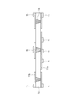
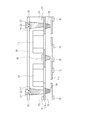
- FIG. 1 is a schematic diagram showing a configuration of a resin multilayer substrate according to Embodiment 1 of the present invention.
- the resin multilayer substrate 1 according to the first embodiment includes a base layer 10, a component built-in layer (first resin layer) 20, and a thin resin layer (second resin layer) 30 stacked in this order. is there.
- the base layer 10 is made of ceramic, glass, epoxy resin or the like, and wiring patterns 11a and 11b are formed on both surfaces.
- An IC element 12 is formed on the surface of the base layer 10 on which the wiring pattern 11a is formed, and a plurality of electronic components 13 are formed on the surface on which the wiring pattern 11b is formed. ).
- the plurality of electronic components 13 are surface-mount components such as a chip capacitor and a resistor.
- the wiring pattern 11 a is electrically connected to the wiring pattern 11 b through a plurality of via conductors 14 formed in the base layer 10. Further, a resist layer 15 is formed at predetermined positions of the wiring patterns 11a and 11b for the purpose of ensuring insulation.
- the component built-in layer 20 is laminated on the surface of the base layer 10 on which the wiring pattern 11b is formed, and incorporates a plurality of mounted electronic components 13 and a part of the wiring pattern 11b.
- the component built-in layer 20 is made of a thermosetting resin such as an epoxy resin, and has a thickness that prevents at least the plurality of electronic components 13 from being exposed to the outside.
- the component built-in layer 20 is formed with a plurality of via conductors (first via conductors) 23 in which a plurality of via holes (first via holes) 21 are filled with a conductive paste 22. One end of the plurality of via conductors 23 reaches one surface of the component built-in layer 20 on which the thin resin layer 30 is laminated, and the other end is electrically connected to the wiring pattern 11b.
- the thin resin layer 30 is sufficiently thinner than the component built-in layer 20 and is laminated on one surface of the component built-in layer 20 so that the component built-in layer 20 is sandwiched between the base layer 10.
- the thin resin layer 30 is made of a thermosetting resin such as an epoxy resin.
- the thin resin layer 30 is formed with a plurality of via conductors (second via conductors) 33 in which a plurality of via holes (second via holes) 31 are filled with the conductive paste 22.
- the plurality of via conductors 33 have a surface electrode 34 formed on the surface of the thin resin layer 30 on the side opposite to the surface laminated on the component built-in layer 20 and a plurality of via conductors 23 on the other end. Are electrically connected to each other.
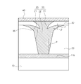
- a part of the thin resin layer 30 in contact with the plurality of via conductors 33 forms a shape 35 protruding into the plurality of via conductors 23 formed in the component built-in layer 20. Therefore, the contact area between a part of the thin resin layer 30 in contact with the plurality of via conductors 33 and the conductive paste 22 is widened. Therefore, the bonding force between the thin resin layer 30 and the plurality of via conductors 33 is increased, and the possibility that the surface electrode 34 is peeled from the thin resin layer 30 together with the conductive paste 22 can be reduced.
- a resist layer 36 is also formed at a predetermined position of the surface electrode 34 for the purpose of ensuring insulation.
- FIG. 2 to 11 are schematic diagrams for explaining a method for manufacturing the resin multilayer substrate 1 according to Embodiment 1 of the present invention.
- 2 shows a state in which the base layer 10 is prepared
- FIG. 3 shows a state in which a plurality of electronic components 13 are mounted on the base layer 10
- FIG. 4 shows a state in which the component built-in layer 20 is laminated on the base layer 10.
- 5 shows a state in which a plurality of via holes 21 are formed in the component built-in layer 20
- FIG. 6 shows a state in which a thin resin layer 30 in which a plurality of via holes 31 are formed is laminated on the component built-in layer 20.
- FIG. 7 shows communication processing performed for the plurality of via holes 21 and 31.
- FIG. 8 shows a state in which the plurality of via holes 21 and 31 are filled with the conductive paste 22
- FIG. 9 shows a state in which the conductive paste 22 protrudes upward from the plurality of via holes 31
- FIG. 11 shows a state in which the metal foil is attached to the thin resin layer 30, and
- FIG. 11 shows a state in which the surface electrode 34 is formed by patterning the metal foil.
- wiring patterns 11a and 11b are formed on both surfaces of the base layer 10, and the base layer 10 has a plurality of wiring patterns 11a and 11b for electrically connecting the wiring patterns 11b.
- a via conductor 14 is formed.
- the wiring patterns 11a and 11b can be formed by patterning a metal layer (for example, Cu layer) formed on each surface of the base layer 10 into a predetermined pattern using photolithography.
- the resist layer 15 formed on the wiring patterns 11a and 11b can also be formed using photolithography in the same manner as the wiring patterns 11a and 11b.
- the base layer 10 may be a resin substrate typified by FR4, or a ceramic substrate such as alumina or LTCC (low temperature sintered ceramic).
- a plurality of electronic components 13 are mounted on the surface of the base layer 10 on which the wiring pattern 11b is formed using a conductive bonding material (not shown) such as solder.
- the component built-in layer 20 is formed on the surface of the base layer 10 on which the plurality of electronic components 13 are mounted so as to incorporate the plurality of electronic components 13 and part of the wiring pattern 11 b.
- the component built-in layer 20 covers the surface on which the plurality of electronic components 13 of the base layer 10 are mounted with an uncured resin sheet, for example, a resin sheet made of epoxy resin, and presses the resin sheet to make it cured. Form.
- the component built-in layer 20 is preferably in a cured state before the thin resin layer 30 is laminated.
- a plurality of bottomed via holes (first via holes) 21 are formed at predetermined positions of the component built-in layer 20.
- the plurality of via holes 21 can be formed by irradiating a predetermined position of the component built-in layer 20 with laser light from the component built-in layer 20 side to the base layer 10 side.
- the cross-sectional shape of the plurality of via holes 21 is a tapered shape in which the diameter decreases as it approaches the base layer 10 because the laser beam is irradiated from the component built-in layer 20 side.
- the plurality of via holes 21 are formed until reaching the wiring pattern 11b.
- a desmear process is performed in which residues in the plurality of via holes 21 are dissolved and removed with concentrated sulfuric acid, chromic acid, or an acid mixed with these. Since the desmear process is a wet process, the resin multilayer substrate 1 after the desmear process is dried.
- the thin resin layer 30 in which the plurality of via holes 31 are formed is laminated on the component built-in layer 20 so that the plurality of via holes 21 and the plurality of via holes 31 are connected.
- the thin resin layer 30 is made of a thermosetting resin such as an epoxy resin, and is in an uncured state when it is laminated on the component built-in layer 20. Therefore, a holding film 38 for holding the shape of a PET film or the like is attached to the thin resin layer 30. With the holding film 38 attached to the thin resin layer 30, a plurality of via holes (second via holes) 31 are formed in the thin resin layer 30 by irradiating laser light from the holding film 38 side.
- a plurality of via holes (third via holes) 39 connected to the plurality of via holes 31 are formed in the holding film 38.
- the cross-sectional shape of the via holes 31 and 39 is a tapered shape whose diameter decreases from the holding film 38 side to the thin resin layer 30 side.
- the thin resin layer 30 to which the holding film 38 is attached is attached to the component built-in layer 20 so that the thin resin layer 30 side is in contact with the component built-in layer 20.
- the diameters of the upper end side and the lower end side of the via hole 31 are formed to be smaller than the diameter of the upper end side of the via hole 21.
- the lower end side of the via hole 31 indicates the side connected to the via hole 21, and the upper end side of the via hole 31 indicates the opposite side of the side connected to the via hole 21. Further, the upper end side of the via hole 21 is a side connected to the via hole 31.
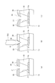
- the thin resin layer 30 in which the via hole 31 is formed is laminated on the component built-in layer 20 so that the via hole 21 formed in the component built-in layer 20 and the via hole 31 are connected, and then the holding film 38 is further formed. It is preferable to perform communication processing (drilling processing) on the via holes 21 and 31 by a method such as laser beam irradiation or pin insertion from the side of the via hole. In a specific communication process (drilling process), the thin resin layer 30 laminated on the component built-in layer 20 is irradiated with laser light having a diameter at least larger than the diameter of the via hole 31 from the holding film 38 side.
- the communication process has a diameter larger than at least the diameter of the via hole 31 in the state of the thin resin layer 30 (FIG. 7A) laminated on the component built-in layer 20, as shown in FIG.
- the pin 300 is inserted from the side of the holding film 38 (FIG. 7B) In the direction of the via hole 21 in a part of the uncured thin resin layer 30 in contact with the via hole 31 by the communication process (drilling process).
- a part of the thin resin layer 30 in contact with the via hole 31 is deformed into a shape protruding in the direction of the via hole 21 (FIG. 7C).
- the via hole 31 may be crushed because the thin resin layer 30 is in an uncured state.
- the connection between the via hole 21 and the via hole 31 can be ensured by performing a communication process (drilling process).
- the conductive paste 22 is filled into the plurality of via holes 21, 31, 39 with the holding film 38 attached to the thin resin layer 30.
- the conductive paste 22 is a paste obtained by mixing a metal powder such as silver, copper, or tin with a solvent or the like.
- the conductive film 22 filled in the via holes 39 formed in the holding film 38 protrudes upward from the plurality of via holes 31 by peeling the holding film 38 from the thin resin layer 30.
- the conductive paste 22 protrudes into the shape. Note that the amount of the conductive paste 22 protruding from the plurality of via holes 31 can be controlled by changing the thickness of the holding film 38.
- a metal foil 40 (for example, copper foil) is attached to the thin resin layer 30.
- the metal foil 40 is attached to the uncured thin resin layer 30, and then the thin resin layer 30 is cured to firmly bond the metal foil 40 and the component built-in layer 20 together. That is, the thin resin layer 30 functions as a bonding layer that bonds the metal foil 40 and the component built-in layer 20 together.
- the conductive paste 22 protruding from the plurality of via holes 31 shown in FIG. 9 is pushed into the plurality of via holes 31.
- the metal foil 40 has a cross-sectional area larger than the cross-sectional area of the plurality of via holes 31 on the side where the conductive paste 22 protrudes (the cross-sectional area on the surface of the via hole 31 in contact with the metal foil 40), the plurality of via holes The conductive paste 22 protruding from 31 can be pushed into the plurality of via holes 31 without leaving.
- a part of the uncured thin resin layer 30 in contact with the plurality of via conductors 33 is directed toward the plurality of via holes 21.
- a force is applied, and a part of the thin resin layer 30 in contact with the plurality of via conductors 33 is deformed into a shape protruding in the direction of the plurality of via holes 21.
- the conductive paste 22 and the thin resin layer 30 are cured to form a shape 35 in which a part of the thin resin layer 30 in contact with the plurality of via conductors 33 protrudes into the plurality of via conductors 23. It will be.
- the conductive paste 22 protruding from the plurality of via holes 31 into the via holes 21 and 31 the density of the conductive paste 22 in the via holes 21 and 31 is increased, and the conductive paste 22 is cured.
- the resistance value of the conductors 23 and 33 is reduced.
- the surface electrode 34 is formed by patterning the metal foil 40 into a predetermined pattern using photolithography. Thereafter, as shown in FIG. 1, a resist layer 36 is formed at a predetermined position of the surface electrode 34 using photolithography, and an IC is formed on the base layer 10 on the wiring pattern 11 a side using a conductive bonding material such as solder. The element 12 is mounted.
- the resin multilayer substrate 1 includes at least the component built-in layer 20 and the thin resin layer 30 laminated on one surface of the component built-in layer 20, and includes a plurality of via conductors.
- a part of the thin resin layer 30 in contact with 33 forms a shape 35 protruding inside the plurality of via conductors 23, that is, in the planar direction and the thickness direction of the component built-in layer 20. Therefore, the contact area between the thin resin layer 30 and the conductive paste 22 is widened, the bonding force between the thin resin layer 30 and the plurality of via conductors 33 is increased, and the thin resin layer 30 and the conductive paste 22 together. The possibility that the surface electrode 34 peels can be reduced.
- the plurality of via holes 31 are stacked. 21 and the plurality of via holes 31 are filled with the conductive paste 22, so that the conductive paste 22 does not enter the interface between the laminated component built-in layer 20 and the thin resin layer 30, and the component built-in layer 20 and the thin resin The insulation performance with the layer 30 is not deteriorated.
- a part of the thin resin layer 30 in contact with the plurality of via conductors 33 is formed inside the plurality of via conductors 23 filled with the conductive paste 22. Since the conductive paste 22 and the thin resin layer 30 are set in a cured state by protruding in the direction, a shape in which a part of the thin resin layer 30 in contact with the via conductor 33 protrudes into the via conductor 23 is formed. Can do. Therefore, a part of the thin resin layer 30 in contact with the via conductor 33 pushes the conductive paste 22 into the plurality of via holes 21 and 31 to increase the density of the conductive paste 22 in the plurality of via holes 21 and 31. The resistance values 23 and 33 can be reduced.
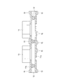
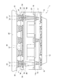
- FIG. 12 is a schematic diagram showing a configuration of the resin multilayer substrate 1 according to the first embodiment of the present invention mounted on the mother substrate.
- the resin multilayer substrate 1 is mounted on the mother substrate 42 by forming solder bumps 41 on the surface electrodes 34 and connecting the solder bumps 41 to the electrodes 43 formed on the mother substrate 42.
- substrate 42 is an electronic circuit board for mounting the some resin multilayer substrate 1 and the electronic component 13, and electrically connecting each.
- the resin multilayer substrate 1 according to the first embodiment is not limited to the one provided with the base layer 10 as shown in FIG. 1, and may be the resin multilayer substrate 1 not provided with the base layer 10.
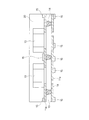
- FIG. 13 is a schematic diagram showing a configuration of the resin multilayer substrate 1 according to Embodiment 1 of the present invention that does not include the base layer 10.
- the resin multilayer substrate 1 has a component built-in layer 20 and a thin resin layer 30 laminated in order, and does not include the base layer 10.
- the component built-in layer 20 includes a wiring pattern 25 on the surface opposite to the surface on which the thin resin layer 30 is laminated, and incorporates a plurality of electronic components 13 mounted on the wiring pattern 25. Since other configurations are the same as those of the resin multilayer substrate 1 shown in FIG. 1, the same components are denoted by the same reference numerals, and detailed description thereof is omitted.
- FIG. 14 shows a state in which the metal foil 40 is attached to the thin resin layer 30 after the conductive vias 22 are filled in the connected via holes 21 and 31, and the metal foil 40 is pressed in the direction of the thin resin layer 30.
- FIG. 15 shows a state after the metal foil 40 is pressed in the direction of the thin resin layer 30.
- the manufacturing method of the resin multilayer substrate 1 according to the second embodiment is shown in FIG. 2 except that the holding film 38 is not attached to the thin resin layer 30 and the thin resin layer 30 alone is laminated on the component built-in layer 20.
- the metal foil 40 is attached to the thin resin layer 30 after the conductive vias 22 are filled in the connected via holes 21 and 31, and in the direction of the arrow 51 (the direction of the thin resin layer 30).
- the metal foil 40 is pressurized.
- the metal foil 40 is pressed in the direction of the arrow 51, the thickness of the uncured thin resin layer 30 is reduced, and the metal foil 40 tends to spread in the direction of the arrow 52.
- the thin resin layer 30 spreading in the direction of the arrow 52 is pushed into the via conductors 23 and 33 as shown in FIG.
- the thin resin layer 30 pushed into the via conductors 23 and 33 is pressurized in the direction of the arrow 51 and protrudes in the direction of the arrow 53 from the via conductor 33 toward the via conductor 23. That is, by pressing the metal foil 40 in the direction of the arrow 51, the thin resin layer 30 is pressed in the direction of the component built-in layer 20, and a part of the thin resin layer 30 in contact with the via conductor 33 becomes part of the via conductor. Thus, a shape 35 protruding into the interior of 23 is formed. Since the subsequent manufacturing method is the same as the manufacturing method shown in FIG. 11, detailed description thereof is omitted.
- the resin multilayer substrate 1 adds the thin resin layer 30 after the conductive paste 22 is filled into the connected via holes 21 and 31 in the direction of the component built-in layer 20.
- a shape 35 in which a part of the thin resin layer 30 in contact with the via conductor 33 protrudes into the via conductor 23 is formed. Therefore, the conductive paste 22 is pushed into the via holes 21 and 31 as much as the thickness of the thin resin layer 30 is reduced by the pressurization, and the density of the conductive paste 22 in the via holes 21 and 31 is increased.
- the resistance value of the via conductors 23 and 33 can be reduced.
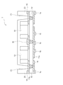
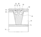
- FIG. 16 is a schematic diagram showing the configuration of the via holes 21 and 31 of the resin multilayer substrate 1 according to Embodiment 3 of the present invention.
- the via conductors 23 and 33 connected to the resin multilayer substrate 1 and the vicinity thereof are illustrated, but other configurations are the same as those of the resin multilayer substrate 1 shown in FIG. Therefore, illustration is abbreviate
- FIG. 16 shows an example in which the taper angle of the via hole 21 changes stepwise for the sake of explanation. In the actual resin multilayer substrate 1, the taper angle of the via hole 21 changes continuously.
- the taper angle refers to an angle formed between a perpendicular to the surface of the base layer 10 on which the wiring pattern 11b is formed and the surface of the component built-in layer 20 on which the via hole 21 is formed.
- the via hole 21 formed in the component built-in layer 20 has an angle ⁇ , an angle ⁇ , an angle ⁇ ( ⁇ ⁇ ) between the vicinity of the wiring pattern 11 b and the vicinity of the thin resin layer 30. ⁇ ) increases in order.
- the taper angle of the via hole 21 is not limited to a case where the taper angle is increased in three stages. If the taper angle of at least the vicinity of the thin resin layer 30 is larger than the taper angle of other parts, the taper angle is not limited to two stages. It may be large or continuously large.
- Making the taper angle of the via hole 21 in the vicinity of the thin resin layer 30 larger than the taper angle of the other part removes the component built-in layer 20 that supports a part of the thin resin layer 30 in contact with the via conductor 33. become.
- a part of the thin resin layer 30 in contact with the via conductor 33 without the supporting component built-in layer 20 is in an uncured state, and therefore bends into the via conductor 23 by its own weight and travels from the via conductor 33 toward the via conductor 23.
- a shape 35 in which a part of the thin resin layer 30 in contact with the via conductor 33 protrudes into the via conductor 23 can be formed only by forming the via hole 21 having a taper angle larger than that of the other portion.
- the plurality of via holes 21 are formed so that the taper angle in the vicinity of the thin resin layer 30 is larger than the taper angle in other parts. . Therefore, a part of the thin resin layer 30 in contact with the via conductor 33 forms a shape 35 protruding into the via conductor 23, so that the contact area between the thin resin layer 30 and the conductive paste 22 is widened. Therefore, the bonding force between the thin resin layer 30 and the via conductor 33 is increased, and the possibility that the surface electrode 34 is peeled from the thin resin layer 30 together with the conductive paste 22 can be reduced.
- all the portions of the thin resin layer 30 in contact with the plurality of via conductors 33 have a shape 35 protruding substantially uniformly into the plurality of via conductors 23.
- the present invention is not limited to the case where it is formed. At least a part of the thin resin layer 30 in contact with the plurality of via conductors 33 may form a shape 35 protruding into the plurality of via conductors 23.
Landscapes
- Engineering & Computer Science (AREA)
- Microelectronics & Electronic Packaging (AREA)
- Manufacturing & Machinery (AREA)
- Production Of Multi-Layered Print Wiring Board (AREA)
- Printing Elements For Providing Electric Connections Between Printed Circuits (AREA)
Abstract
Description
図1は、本発明の実施の形態1に係る樹脂多層基板の構成を示す模式図である。図1に示すように、実施の形態1に係る樹脂多層基板1は、ベース層10、部品内蔵層(第1樹脂層)20、薄層樹脂層(第2樹脂層)30を順に積層してある。ベース層10は、セラミック、ガラス、エポキシ樹脂等で構成され、両面に配線パターン11a、11bが形成してある。ベース層10の、配線パターン11aが形成してある面には、IC素子12が、配線パターン11bが形成してある面には複数の電子部品13がはんだ等の導電性接合材(図示せず)を用いて実装されている。複数の電子部品13は、表面実装型の部品であり、例えばチップコンデンサ、抵抗等である。配線パターン11aは、ベース層10に形成してある複数のビア導体14を介して配線パターン11bと電気的に接続している。また、配線パターン11a、11bの所定位置には、絶縁性を確保する等の理由からレジスト層15が形成してある。
図14及び図15は、本発明の実施の形態2に係る樹脂多層基板1の製造方法を説明するための模式図である。図14は、連接したビアホール21、31に導電性ペースト22を充填した後の薄層樹脂層30に金属箔40を貼り付け、薄層樹脂層30の方向に金属箔40を加圧する状態を、図15は、薄層樹脂層30の方向に金属箔40を加圧した後の状態を、それぞれ示している。本実施の形態2に係る樹脂多層基板1の製造方法は、保持フィルム38を薄層樹脂層30に貼り付けず、薄層樹脂層30単体を部品内蔵層20に積層する以外、図2から図8で示した実施の形態1の製造方法と同じであるため、詳細な説明を省略する。なお、図14及び図15では、樹脂多層基板1に形成した連接するビア導体23、33とその近傍部分について図示しているが、他の構成については図1に示す樹脂多層基板1の構成と同じであるため図示を省略している。
図16は、本発明の実施の形態3に係る樹脂多層基板1のビアホール21、31の構成を示す模式図である。なお、図16では、樹脂多層基板1に形成した連接するビア導体23、33とその近傍部分について図示しているが、他の構成については図1に示す樹脂多層基板1の構成と同じであるため図示を省略している。なお、図16では、説明のためにビアホール21のテーパー角が段階的に変化する例を示しているが、実際の樹脂多層基板1では、ビアホール21のテーパー角は連続的に変化している。なお、テーパー角とは、配線パターン11bが形成されたベース層10の面に対する垂線と、ビアホール21が形成された部品内蔵層20の面とのなす角度をいう。
10 ベース層
20 部品内蔵層
30 薄層樹脂層
11a、11b 配線パターン
12 IC素子
13 電子部品
14、23、33 ビア導体
15、36 レジスト層
21、31 ビアホール
22 導電性ペースト
34 表面電極
35 ビア導体の内部へ突き出した形状
38 保持フィルム
Claims (12)
- 第1樹脂層と、該第1樹脂層の一面に積層してある第2樹脂層とを備える樹脂多層基板において、
前記第2樹脂層の、前記第1樹脂層に積層されている面とは反対側の面に形成してある表面電極と、
前記第1樹脂層に設けてあり、一端が前記第1樹脂層の前記一面に至る第1ビア導体と、
前記第2樹脂層に設けてあり、一端が前記表面電極と、他端が前記第1ビア導体とそれぞれ電気的に接続してある第2ビア導体と
を備え、
前記第2ビア導体と接する前記第2樹脂層の少なくとも一部が、前記第1ビア導体の内部へ突き出した形状を形成していることを特徴とする樹脂多層基板。 - 少なくとも一面に配線パターンを形成してあるベース層を備え、
前記配線パターンが形成してある前記ベース層の一面に、前記第1樹脂層、前記第2樹脂層を順に積層し、前記配線パターンと前記第1ビア導体とを電気的に接続してあることを特徴とする請求項1に記載の樹脂多層基板。 - 前記第1樹脂層の、前記第2樹脂層が積層してある面とは反対側の面に形成してある配線パターンと、
前記第1樹脂層に内蔵し、前記配線パターンに実装してある電子部品とを備えることを特徴とする請求項1に記載の樹脂多層基板。 - 前記ベース層の少なくとも一面に電子部品を実装し、実装してある前記電子部品を前記第1樹脂層に内蔵してあることを特徴とする請求項2に記載の樹脂多層基板。
- 前記表面電極は、マザー基板に形成されている電極と電気的に接続してあることを特徴とする請求項1乃至4のいずれか一項に記載の樹脂多層基板。
- 前記第1ビア導体は、前記第2樹脂層の近傍部分のテーパー角が他の部分のテーパー角よりも大きくなるように形成してあることを特徴とする請求項1乃至5のいずれか一項に記載の樹脂多層基板。
- 第1樹脂層と、該第1樹脂層の一面に積層してある第2樹脂層とを備える樹脂多層基板を製造する方法において、
硬化状態の第1樹脂層に第1ビアホールを形成する第1工程と、
未硬化状態の第2樹脂層に第2ビアホールを形成し、前記第1ビアホールと前記第2ビアホールとが連接するように、前記第1樹脂層の一面に前記第2樹脂層を積層する第2工程と、
前記第1ビアホール及び前記第2ビアホールに導電性ペーストを充填して第1ビア導体及び第2ビア導体を形成する第3工程と、
前記第2ビア導体と接する前記第2樹脂層の少なくとも一部を、前記第1ビア導体の内部へ突き出す第4工程と、
前記導電性ペースト及び前記第2樹脂層を硬化状態にする第5工程と
を含むことを特徴とする樹脂多層基板の製造方法。 - 前記第3工程では、
前記第1ビアホール及び前記第2ビアホールに導電性ペーストを充填した場合、前記第2ビアホールから少なくとも上に凸形状を有するように前記導電性ペーストがはみ出し、
前記第4工程では、
前記第2ビアホールからはみ出した前記導電性ペーストを、前記導電性ペーストがはみ出した側の前記第2ビアホールの断面積よりも大きい断面積を有する物体で、前記第2ビアホール内へ押し込むことで、前記第2ビア導体と接する前記第2樹脂層の少なくとも一部を、前記第1ビア導体の内部へ突き出すことを特徴とする請求項7に記載の樹脂多層基板の製造方法。 - 未硬化状態の前記第2樹脂層の一面に、前記第2樹脂層の形状を保持する保持フィルムが貼り付けられ、貼り付けられた保持フィルムに前記第2樹脂層に形成した前記第2ビアホールと連接する第3ビアホールが形成してあり、
前記第3工程では、前記第1ビアホール、前記第2ビアホール、前記第3ビアホールに導電性ペーストを充填し、
前記第3工程の終了後に、前記保持フィルムを前記第2樹脂層から剥離することで、前記保持フィルムに形成してある前記第3ビアホールに充填されている前記導電性ペーストを、前記第2ビアホールからはみ出した前記導電性ペーストとすることを特徴とする請求項8に記載の樹脂多層基板の製造方法。 - 前記第4工程では、
前記第2樹脂層を前記第1樹脂層の方向に加圧することで、前記第2ビア導体と接する前記第2樹脂層の少なくとも一部を、前記第1ビア導体の内部へ突き出すことを特徴とする請求項7に記載の樹脂多層基板の製造方法。 - 前記第1工程では、
前記第2樹脂層の近傍部分のテーパー角が、他の部分のテーパー角よりも大きくなるように前記第1ビアホールを形成することを特徴とする請求項7に記載の樹脂多層基板の製造方法。 - 前記第2工程では、
前記第1樹脂層の一面に前記第2樹脂層を積層した後、前記第1ビアホール及び前記第2ビアホールに対して連通処理を行うことを特徴とする請求項7に記載の樹脂多層基板の製造方法。
Priority Applications (4)
| Application Number | Priority Date | Filing Date | Title |
|---|---|---|---|
| JP2011528791A JP5206878B2 (ja) | 2009-08-24 | 2010-08-24 | 樹脂多層基板及び該樹脂多層基板の製造方法 |
| CN201080037256.XA CN102484950B (zh) | 2009-08-24 | 2010-08-24 | 树脂多层基板以及该树脂多层基板的制造方法 |
| KR1020127003363A KR101319902B1 (ko) | 2009-08-24 | 2010-08-24 | 수지 다층 기판 및 그 수지 다층 기판의 제조방법 |
| US13/403,042 US8890002B2 (en) | 2009-08-24 | 2012-02-23 | Resin multilayer substrate and method for manufacturing the resin multilayer substrate |
Applications Claiming Priority (4)
| Application Number | Priority Date | Filing Date | Title |
|---|---|---|---|
| JP2009-192688 | 2009-08-24 | ||
| JP2009192688 | 2009-08-24 | ||
| JP2009-249622 | 2009-10-30 | ||
| JP2009249622 | 2009-10-30 |
Related Child Applications (1)
| Application Number | Title | Priority Date | Filing Date |
|---|---|---|---|
| US13/403,042 Continuation US8890002B2 (en) | 2009-08-24 | 2012-02-23 | Resin multilayer substrate and method for manufacturing the resin multilayer substrate |
Publications (1)
| Publication Number | Publication Date |
|---|---|
| WO2011024790A1 true WO2011024790A1 (ja) | 2011-03-03 |
Family
ID=43627895
Family Applications (1)
| Application Number | Title | Priority Date | Filing Date |
|---|---|---|---|
| PCT/JP2010/064253 Ceased WO2011024790A1 (ja) | 2009-08-24 | 2010-08-24 | 樹脂多層基板及び該樹脂多層基板の製造方法 |
Country Status (5)
| Country | Link |
|---|---|
| US (1) | US8890002B2 (ja) |
| JP (1) | JP5206878B2 (ja) |
| KR (1) | KR101319902B1 (ja) |
| CN (1) | CN102484950B (ja) |
| WO (1) | WO2011024790A1 (ja) |
Cited By (5)
| Publication number | Priority date | Publication date | Assignee | Title |
|---|---|---|---|---|
| JP2014131029A (ja) * | 2012-12-31 | 2014-07-10 | Samsung Electro-Mechanics Co Ltd | 回路基板及びその製造方法 |
| JP2015076481A (ja) * | 2013-10-08 | 2015-04-20 | 株式会社村田製作所 | セラミック多層基板 |
| WO2020045528A1 (ja) * | 2018-08-31 | 2020-03-05 | 株式会社村田製作所 | 配線基板およびモジュール |
| JP2024058397A (ja) * | 2022-10-14 | 2024-04-25 | 株式会社村田製作所 | インダクタ部品 |
| JP2024058406A (ja) * | 2022-10-14 | 2024-04-25 | 株式会社村田製作所 | インダクタ部品 |
Families Citing this family (8)
| Publication number | Priority date | Publication date | Assignee | Title |
|---|---|---|---|---|
| US9728563B2 (en) * | 2012-10-26 | 2017-08-08 | Applied Materials, Inc. | Combinatorial masking |
| WO2015068555A1 (ja) * | 2013-11-07 | 2015-05-14 | 株式会社村田製作所 | 多層基板およびその製造方法 |
| US9510454B2 (en) | 2014-02-28 | 2016-11-29 | Qualcomm Incorporated | Integrated interposer with embedded active devices |
| KR101983168B1 (ko) | 2014-04-08 | 2019-05-28 | 삼성전기주식회사 | 전자 소자 모듈 및 그 제조 방법 |
| JP2016004889A (ja) * | 2014-06-17 | 2016-01-12 | イビデン株式会社 | プリント配線板 |
| US9281284B2 (en) * | 2014-06-20 | 2016-03-08 | Freescale Semiconductor Inc. | System-in-packages having vertically-interconnected leaded components and methods for the fabrication thereof |
| CN109673112B (zh) * | 2017-10-13 | 2021-08-20 | 鹏鼎控股(深圳)股份有限公司 | 柔性电路板以及柔性电路板的制作方法 |
| JP6863244B2 (ja) | 2017-11-20 | 2021-04-21 | 株式会社村田製作所 | 電子部品および電子部品の製造方法 |
Citations (3)
| Publication number | Priority date | Publication date | Assignee | Title |
|---|---|---|---|---|
| JP2001244636A (ja) * | 2000-03-01 | 2001-09-07 | Ibiden Co Ltd | プリント配線板 |
| JP2003069228A (ja) * | 2001-08-23 | 2003-03-07 | Ibiden Co Ltd | 樹脂充填用マスクおよび多層プリント配線板の製造方法 |
| WO2009081853A1 (ja) * | 2007-12-25 | 2009-07-02 | Murata Manufacturing Co., Ltd. | 多層配線基板の製造方法 |
Family Cites Families (15)
| Publication number | Priority date | Publication date | Assignee | Title |
|---|---|---|---|---|
| JPH0722223B2 (ja) * | 1985-08-24 | 1995-03-08 | ソニー株式会社 | フレキシブル配線基板の接続装置および接続方法 |
| JPH01302792A (ja) * | 1988-05-30 | 1989-12-06 | Sharp Corp | 両面配線回路基板の両面回路接続方法 |
| JP2002026520A (ja) * | 2000-07-06 | 2002-01-25 | Matsushita Electric Ind Co Ltd | 多層配線基板及びその製造方法 |
| US6855892B2 (en) * | 2001-09-27 | 2005-02-15 | Matsushita Electric Industrial Co., Ltd. | Insulation sheet, multi-layer wiring substrate and production processes thereof |
| JP4009080B2 (ja) * | 2001-10-02 | 2007-11-14 | イビデン株式会社 | 配線板およびその製造方法 |
| JP2003124380A (ja) | 2001-10-15 | 2003-04-25 | Matsushita Electric Ind Co Ltd | 電子部品内蔵モジュールおよびその製造方法 |
| WO2003071843A1 (en) * | 2002-02-22 | 2003-08-28 | Fujikura Ltd. | Multilayer wiring board, base for multilayer wiring board, printed wiring board, and its manufacturing method |
| JP4059085B2 (ja) * | 2003-01-14 | 2008-03-12 | 松下電器産業株式会社 | 高周波積層部品およびその製造方法 |
| US7211289B2 (en) * | 2003-12-18 | 2007-05-01 | Endicott Interconnect Technologies, Inc. | Method of making multilayered printed circuit board with filled conductive holes |
| WO2007069510A1 (ja) * | 2005-12-12 | 2007-06-21 | Matsushita Electric Industrial Co., Ltd. | 回路基板を製造するための中間材とそれを用いた回路基板の製造方法 |
| JP5021216B2 (ja) * | 2006-02-22 | 2012-09-05 | イビデン株式会社 | プリント配線板およびその製造方法 |
| JP5236379B2 (ja) * | 2007-08-24 | 2013-07-17 | 日本特殊陶業株式会社 | Ic検査装置用基板及びその製造方法 |
| JP2009060076A (ja) * | 2007-08-31 | 2009-03-19 | Samsung Electro Mech Co Ltd | 多層プリント基板の製造方法 |
| US8431832B2 (en) * | 2007-11-28 | 2013-04-30 | Kyocera Corporation | Circuit board, mounting structure, and method for manufacturing circuit board |
| US8925192B2 (en) * | 2009-06-09 | 2015-01-06 | Ibiden Co., Ltd. | Printed wiring board and method for manufacturing the same |
-
2010
- 2010-08-24 JP JP2011528791A patent/JP5206878B2/ja not_active Expired - Fee Related
- 2010-08-24 KR KR1020127003363A patent/KR101319902B1/ko not_active Expired - Fee Related
- 2010-08-24 WO PCT/JP2010/064253 patent/WO2011024790A1/ja not_active Ceased
- 2010-08-24 CN CN201080037256.XA patent/CN102484950B/zh not_active Expired - Fee Related
-
2012
- 2012-02-23 US US13/403,042 patent/US8890002B2/en not_active Expired - Fee Related
Patent Citations (3)
| Publication number | Priority date | Publication date | Assignee | Title |
|---|---|---|---|---|
| JP2001244636A (ja) * | 2000-03-01 | 2001-09-07 | Ibiden Co Ltd | プリント配線板 |
| JP2003069228A (ja) * | 2001-08-23 | 2003-03-07 | Ibiden Co Ltd | 樹脂充填用マスクおよび多層プリント配線板の製造方法 |
| WO2009081853A1 (ja) * | 2007-12-25 | 2009-07-02 | Murata Manufacturing Co., Ltd. | 多層配線基板の製造方法 |
Cited By (11)
| Publication number | Priority date | Publication date | Assignee | Title |
|---|---|---|---|---|
| JP2014131029A (ja) * | 2012-12-31 | 2014-07-10 | Samsung Electro-Mechanics Co Ltd | 回路基板及びその製造方法 |
| JP2015076481A (ja) * | 2013-10-08 | 2015-04-20 | 株式会社村田製作所 | セラミック多層基板 |
| US9686872B2 (en) | 2013-10-08 | 2017-06-20 | Murata Manufacturing Co., Ltd. | Ceramic multilayer substrate |
| WO2020045528A1 (ja) * | 2018-08-31 | 2020-03-05 | 株式会社村田製作所 | 配線基板およびモジュール |
| JPWO2020045528A1 (ja) * | 2018-08-31 | 2021-08-10 | 株式会社村田製作所 | 配線基板およびモジュール |
| US11324108B2 (en) | 2018-08-31 | 2022-05-03 | Murata Manufacturing Co., Ltd. | Wiring substrate and module |
| JP7124874B2 (ja) | 2018-08-31 | 2022-08-24 | 株式会社村田製作所 | モジュール |
| JP2024058397A (ja) * | 2022-10-14 | 2024-04-25 | 株式会社村田製作所 | インダクタ部品 |
| JP2024058406A (ja) * | 2022-10-14 | 2024-04-25 | 株式会社村田製作所 | インダクタ部品 |
| JP7652170B2 (ja) | 2022-10-14 | 2025-03-27 | 株式会社村田製作所 | インダクタ部品 |
| JP7771914B2 (ja) | 2022-10-14 | 2025-11-18 | 株式会社村田製作所 | インダクタ部品 |
Also Published As
| Publication number | Publication date |
|---|---|
| US8890002B2 (en) | 2014-11-18 |
| KR101319902B1 (ko) | 2013-10-18 |
| CN102484950B (zh) | 2014-12-31 |
| JPWO2011024790A1 (ja) | 2013-01-31 |
| US20120145445A1 (en) | 2012-06-14 |
| JP5206878B2 (ja) | 2013-06-12 |
| KR20120031307A (ko) | 2012-04-02 |
| CN102484950A (zh) | 2012-05-30 |
Similar Documents
| Publication | Publication Date | Title |
|---|---|---|
| JP5206878B2 (ja) | 樹脂多層基板及び該樹脂多層基板の製造方法 | |
| KR100811034B1 (ko) | 전자소자 내장 인쇄회로기판의 제조방법 | |
| JP5181702B2 (ja) | 配線基板の製造方法 | |
| JP5022392B2 (ja) | ペーストバンプを用いた印刷回路基板の製造方法 | |
| KR101868680B1 (ko) | 회로 기판, 회로 기판의 제조 방법 및 전자 기기 | |
| US7286367B2 (en) | Printed circuit board with a built-in passive device, manufacturing method of the printed circuit board, and elemental board for the printed circuit board | |
| JP6139653B2 (ja) | 部品内蔵樹脂多層基板 | |
| JP5163806B2 (ja) | 部品内蔵モジュールの製造方法及び部品内蔵モジュール | |
| CN107516764B (zh) | 天线结构及其制作方法 | |
| KR20080026028A (ko) | 반도체 장치의 제조방법 | |
| JP2001332866A (ja) | 回路基板及びその製造方法 | |
| JP5223361B2 (ja) | 配線基板の製造方法 | |
| TWI498056B (zh) | 具有內埋元件的電路板、其製作方法及封裝結構 | |
| US20090288293A1 (en) | Metal core package substrate and method for manufacturing the same | |
| KR102914349B1 (ko) | 회로 기판, 회로 기판의 제조 방법, 및 전자 기기 | |
| JP2008300819A (ja) | プリント基板およびその製造方法 | |
| JP2012064600A (ja) | 多層基板およびその製造方法 | |
| JP2005026573A (ja) | 部品内蔵モジュールの製造方法 | |
| CN104637913A (zh) | 电子元件模块及其制造方法 | |
| JP5672675B2 (ja) | 樹脂多層基板 | |
| JP2011044523A (ja) | 樹脂多層基板及び該樹脂多層基板の製造方法 | |
| KR100704922B1 (ko) | 페이스트 범프를 이용한 인쇄회로기판 및 그 제조방법 | |
| JP2011061010A (ja) | 部品内蔵モジュールの製造方法 | |
| JP5323395B2 (ja) | 電子モジュール、電子モジュールの製造方法 | |
| JP5108253B2 (ja) | 部品実装モジュール |
Legal Events
| Date | Code | Title | Description |
|---|---|---|---|
| WWE | Wipo information: entry into national phase |
Ref document number: 201080037256.X Country of ref document: CN |
|
| 121 | Ep: the epo has been informed by wipo that ep was designated in this application |
Ref document number: 10811840 Country of ref document: EP Kind code of ref document: A1 |
|
| WWE | Wipo information: entry into national phase |
Ref document number: 2011528791 Country of ref document: JP |
|
| ENP | Entry into the national phase |
Ref document number: 20127003363 Country of ref document: KR Kind code of ref document: A |
|
| NENP | Non-entry into the national phase |
Ref country code: DE |
|
| 122 | Ep: pct application non-entry in european phase |
Ref document number: 10811840 Country of ref document: EP Kind code of ref document: A1 |