WO2011007874A1 - Ledチップ接合体、ledパッケージ、及びledパッケージの製造方法 - Google Patents
Ledチップ接合体、ledパッケージ、及びledパッケージの製造方法 Download PDFInfo
- Publication number
- WO2011007874A1 WO2011007874A1 PCT/JP2010/062102 JP2010062102W WO2011007874A1 WO 2011007874 A1 WO2011007874 A1 WO 2011007874A1 JP 2010062102 W JP2010062102 W JP 2010062102W WO 2011007874 A1 WO2011007874 A1 WO 2011007874A1
- Authority
- WO
- WIPO (PCT)
- Prior art keywords
- led chip
- led
- composite substrate
- metal
- aluminum
- Prior art date
Links
Images


Classifications
-
- H—ELECTRICITY
- H01—ELECTRIC ELEMENTS
- H01L—SEMICONDUCTOR DEVICES NOT COVERED BY CLASS H10
- H01L33/00—Semiconductor devices with at least one potential-jump barrier or surface barrier specially adapted for light emission; Processes or apparatus specially adapted for the manufacture or treatment thereof or of parts thereof; Details thereof
- H01L33/48—Semiconductor devices with at least one potential-jump barrier or surface barrier specially adapted for light emission; Processes or apparatus specially adapted for the manufacture or treatment thereof or of parts thereof; Details thereof characterised by the semiconductor body packages
- H01L33/64—Heat extraction or cooling elements
- H01L33/641—Heat extraction or cooling elements characterized by the materials
-
- H—ELECTRICITY
- H01—ELECTRIC ELEMENTS
- H01L—SEMICONDUCTOR DEVICES NOT COVERED BY CLASS H10
- H01L2224/00—Indexing scheme for arrangements for connecting or disconnecting semiconductor or solid-state bodies and methods related thereto as covered by H01L24/00
- H01L2224/01—Means for bonding being attached to, or being formed on, the surface to be connected, e.g. chip-to-package, die-attach, "first-level" interconnects; Manufacturing methods related thereto
- H01L2224/26—Layer connectors, e.g. plate connectors, solder or adhesive layers; Manufacturing methods related thereto
- H01L2224/31—Structure, shape, material or disposition of the layer connectors after the connecting process
- H01L2224/32—Structure, shape, material or disposition of the layer connectors after the connecting process of an individual layer connector
- H01L2224/321—Disposition
- H01L2224/32151—Disposition the layer connector connecting between a semiconductor or solid-state body and an item not being a semiconductor or solid-state body, e.g. chip-to-substrate, chip-to-passive
- H01L2224/32221—Disposition the layer connector connecting between a semiconductor or solid-state body and an item not being a semiconductor or solid-state body, e.g. chip-to-substrate, chip-to-passive the body and the item being stacked
- H01L2224/32225—Disposition the layer connector connecting between a semiconductor or solid-state body and an item not being a semiconductor or solid-state body, e.g. chip-to-substrate, chip-to-passive the body and the item being stacked the item being non-metallic, e.g. insulating substrate with or without metallisation
-
- H—ELECTRICITY
- H01—ELECTRIC ELEMENTS
- H01L—SEMICONDUCTOR DEVICES NOT COVERED BY CLASS H10
- H01L2224/00—Indexing scheme for arrangements for connecting or disconnecting semiconductor or solid-state bodies and methods related thereto as covered by H01L24/00
- H01L2224/01—Means for bonding being attached to, or being formed on, the surface to be connected, e.g. chip-to-package, die-attach, "first-level" interconnects; Manufacturing methods related thereto
- H01L2224/42—Wire connectors; Manufacturing methods related thereto
- H01L2224/44—Structure, shape, material or disposition of the wire connectors prior to the connecting process
- H01L2224/45—Structure, shape, material or disposition of the wire connectors prior to the connecting process of an individual wire connector
- H01L2224/45001—Core members of the connector
- H01L2224/45099—Material
- H01L2224/451—Material with a principal constituent of the material being a metal or a metalloid, e.g. boron (B), silicon (Si), germanium (Ge), arsenic (As), antimony (Sb), tellurium (Te) and polonium (Po), and alloys thereof
- H01L2224/45138—Material with a principal constituent of the material being a metal or a metalloid, e.g. boron (B), silicon (Si), germanium (Ge), arsenic (As), antimony (Sb), tellurium (Te) and polonium (Po), and alloys thereof the principal constituent melting at a temperature of greater than or equal to 950°C and less than 1550°C
- H01L2224/45144—Gold (Au) as principal constituent
-
- H—ELECTRICITY
- H01—ELECTRIC ELEMENTS
- H01L—SEMICONDUCTOR DEVICES NOT COVERED BY CLASS H10
- H01L2224/00—Indexing scheme for arrangements for connecting or disconnecting semiconductor or solid-state bodies and methods related thereto as covered by H01L24/00
- H01L2224/01—Means for bonding being attached to, or being formed on, the surface to be connected, e.g. chip-to-package, die-attach, "first-level" interconnects; Manufacturing methods related thereto
- H01L2224/42—Wire connectors; Manufacturing methods related thereto
- H01L2224/47—Structure, shape, material or disposition of the wire connectors after the connecting process
- H01L2224/48—Structure, shape, material or disposition of the wire connectors after the connecting process of an individual wire connector
- H01L2224/4805—Shape
- H01L2224/4809—Loop shape
- H01L2224/48091—Arched
-
- H—ELECTRICITY
- H01—ELECTRIC ELEMENTS
- H01L—SEMICONDUCTOR DEVICES NOT COVERED BY CLASS H10
- H01L2224/00—Indexing scheme for arrangements for connecting or disconnecting semiconductor or solid-state bodies and methods related thereto as covered by H01L24/00
- H01L2224/01—Means for bonding being attached to, or being formed on, the surface to be connected, e.g. chip-to-package, die-attach, "first-level" interconnects; Manufacturing methods related thereto
- H01L2224/42—Wire connectors; Manufacturing methods related thereto
- H01L2224/47—Structure, shape, material or disposition of the wire connectors after the connecting process
- H01L2224/48—Structure, shape, material or disposition of the wire connectors after the connecting process of an individual wire connector
- H01L2224/481—Disposition
- H01L2224/48151—Connecting between a semiconductor or solid-state body and an item not being a semiconductor or solid-state body, e.g. chip-to-substrate, chip-to-passive
- H01L2224/48221—Connecting between a semiconductor or solid-state body and an item not being a semiconductor or solid-state body, e.g. chip-to-substrate, chip-to-passive the body and the item being stacked
- H01L2224/48225—Connecting between a semiconductor or solid-state body and an item not being a semiconductor or solid-state body, e.g. chip-to-substrate, chip-to-passive the body and the item being stacked the item being non-metallic, e.g. insulating substrate with or without metallisation
- H01L2224/48227—Connecting between a semiconductor or solid-state body and an item not being a semiconductor or solid-state body, e.g. chip-to-substrate, chip-to-passive the body and the item being stacked the item being non-metallic, e.g. insulating substrate with or without metallisation connecting the wire to a bond pad of the item
-
- H—ELECTRICITY
- H01—ELECTRIC ELEMENTS
- H01L—SEMICONDUCTOR DEVICES NOT COVERED BY CLASS H10
- H01L2224/00—Indexing scheme for arrangements for connecting or disconnecting semiconductor or solid-state bodies and methods related thereto as covered by H01L24/00
- H01L2224/73—Means for bonding being of different types provided for in two or more of groups H01L2224/10, H01L2224/18, H01L2224/26, H01L2224/34, H01L2224/42, H01L2224/50, H01L2224/63, H01L2224/71
- H01L2224/732—Location after the connecting process
- H01L2224/73251—Location after the connecting process on different surfaces
- H01L2224/73265—Layer and wire connectors
-
- H—ELECTRICITY
- H01—ELECTRIC ELEMENTS
- H01L—SEMICONDUCTOR DEVICES NOT COVERED BY CLASS H10
- H01L23/00—Details of semiconductor or other solid state devices
- H01L23/12—Mountings, e.g. non-detachable insulating substrates
- H01L23/14—Mountings, e.g. non-detachable insulating substrates characterised by the material or its electrical properties
- H01L23/142—Metallic substrates having insulating layers
-
- H—ELECTRICITY
- H01—ELECTRIC ELEMENTS
- H01L—SEMICONDUCTOR DEVICES NOT COVERED BY CLASS H10
- H01L24/00—Arrangements for connecting or disconnecting semiconductor or solid-state bodies; Methods or apparatus related thereto
- H01L24/73—Means for bonding being of different types provided for in two or more of groups H01L24/10, H01L24/18, H01L24/26, H01L24/34, H01L24/42, H01L24/50, H01L24/63, H01L24/71
-
- H—ELECTRICITY
- H01—ELECTRIC ELEMENTS
- H01L—SEMICONDUCTOR DEVICES NOT COVERED BY CLASS H10
- H01L25/00—Assemblies consisting of a plurality of individual semiconductor or other solid state devices ; Multistep manufacturing processes thereof
- H01L25/03—Assemblies consisting of a plurality of individual semiconductor or other solid state devices ; Multistep manufacturing processes thereof all the devices being of a type provided for in the same subgroup of groups H01L27/00 - H01L33/00, or in a single subclass of H10K, H10N, e.g. assemblies of rectifier diodes
- H01L25/04—Assemblies consisting of a plurality of individual semiconductor or other solid state devices ; Multistep manufacturing processes thereof all the devices being of a type provided for in the same subgroup of groups H01L27/00 - H01L33/00, or in a single subclass of H10K, H10N, e.g. assemblies of rectifier diodes the devices not having separate containers
- H01L25/075—Assemblies consisting of a plurality of individual semiconductor or other solid state devices ; Multistep manufacturing processes thereof all the devices being of a type provided for in the same subgroup of groups H01L27/00 - H01L33/00, or in a single subclass of H10K, H10N, e.g. assemblies of rectifier diodes the devices not having separate containers the devices being of a type provided for in group H01L33/00
- H01L25/0753—Assemblies consisting of a plurality of individual semiconductor or other solid state devices ; Multistep manufacturing processes thereof all the devices being of a type provided for in the same subgroup of groups H01L27/00 - H01L33/00, or in a single subclass of H10K, H10N, e.g. assemblies of rectifier diodes the devices not having separate containers the devices being of a type provided for in group H01L33/00 the devices being arranged next to each other
-
- H—ELECTRICITY
- H01—ELECTRIC ELEMENTS
- H01L—SEMICONDUCTOR DEVICES NOT COVERED BY CLASS H10
- H01L2924/00—Indexing scheme for arrangements or methods for connecting or disconnecting semiconductor or solid-state bodies as covered by H01L24/00
- H01L2924/013—Alloys
- H01L2924/0132—Binary Alloys
- H01L2924/01322—Eutectic Alloys, i.e. obtained by a liquid transforming into two solid phases
-
- H—ELECTRICITY
- H01—ELECTRIC ELEMENTS
- H01L—SEMICONDUCTOR DEVICES NOT COVERED BY CLASS H10
- H01L2924/00—Indexing scheme for arrangements or methods for connecting or disconnecting semiconductor or solid-state bodies as covered by H01L24/00
- H01L2924/15—Details of package parts other than the semiconductor or other solid state devices to be connected
- H01L2924/181—Encapsulation
-
- H—ELECTRICITY
- H01—ELECTRIC ELEMENTS
- H01L—SEMICONDUCTOR DEVICES NOT COVERED BY CLASS H10
- H01L33/00—Semiconductor devices with at least one potential-jump barrier or surface barrier specially adapted for light emission; Processes or apparatus specially adapted for the manufacture or treatment thereof or of parts thereof; Details thereof
- H01L33/48—Semiconductor devices with at least one potential-jump barrier or surface barrier specially adapted for light emission; Processes or apparatus specially adapted for the manufacture or treatment thereof or of parts thereof; Details thereof characterised by the semiconductor body packages
- H01L33/64—Heat extraction or cooling elements
- H01L33/647—Heat extraction or cooling elements the elements conducting electric current to or from the semiconductor body
Definitions
- the present invention relates to an LED chip assembly, an LED package, and a method for manufacturing the LED package.
- An LED light emitting element is an element that emits light when a forward current flows through a pn junction of a semiconductor, and is manufactured using a III-V group semiconductor crystal such as GaAs or GaN.
- LED light emitting devices with excellent conversion efficiency have been developed due to advances in semiconductor epitaxial growth technology and light emitting device process technology, and are widely used in various fields.
- the LED chip is composed of a p-type layer and an n-type layer obtained by epitaxially growing a group III-V semiconductor crystal on a growth substrate, and a photoactive layer sandwiched between both.
- a group III-V semiconductor crystal is epitaxially grown on a growth substrate such as single crystal sapphire, and then an electrode or the like is formed to form an LED chip.
- the single crystal sapphire has a thermal conductivity of about 40 W / (m ⁇ K)
- the heat generated in the III-V group semiconductor device cannot be sufficiently dissipated.
- the temperature of the element rises, causing a decrease in light emission efficiency and a decrease in element life.
- Patent Document 1 was not satisfactory. That is, since the metal package substrate (holding substrate) is also conductive, it must have a non-insulating structure for mounting.
- an object of the present invention is to provide a highly reliable LED package with significantly improved heat dissipation, a method for manufacturing the LED package, and an LED chip assembly used for the LED package.
- the present invention is an LED chip joined body in which one or two or more LED chips are directly mounted on a composite substrate with a joining material, and the composite substrate contains aluminum, silicon, or a component thereof in an inorganic molded body.
- the sheet thickness is 0.1-2 mm
- the surface roughness (Ra) is 0.5 ⁇ m or less
- the thermal conductivity at a temperature of 25 ° C. is 100-600 W / (m ⁇ K)
- the temperature is 25 ° C.
- the linear expansion coefficient at ⁇ 150 ° C. is 3 to 12 ⁇ 10 ⁇ 6 / K
- the three-point bending strength is 50 to 500 MPa
- the area of the LED chip mounting surface of the composite substrate is smaller than the contact area with the LED chip.
- An LED chip joined body having a magnification of 2 to 100 times.
- the present invention also relates to an LED chip assembly in which one or two or more LED chips are directly mounted on a composite substrate with a bonding material, and the composite substrate is an inorganic molding having a porosity of 10 to 40% by volume.
- the body is impregnated with an aluminum-silicon alloy having an aluminum content of 80 to 97% by mass, the plate thickness is 0.1 to 1 mm, the surface roughness (Ra) is 0.5 ⁇ m or less, and the heat conduction is 25 ° C.
- LED chip of a composite substrate with a rate of 100 to 300 W / (m ⁇ K), a linear expansion coefficient of 4 to 9 ⁇ 10 ⁇ 6 / K at a temperature of 25 ° C. to 150 ° C., and a three-point bending strength of 50 to 400 MPa.
- the LED chip assembly is characterized in that the area of the mounting surface is 2 to 25 times the contact area with the LED chip.
- the composite substrate has a thickness of 0.5 at least one metal selected from Ni, Co, Pd, Cu, Ag, Au, Pt and Sn on the surface.
- the bonding material made of the bonding material is soldering, brazing, or a high thermal conductive adhesive; and
- the material of the inorganic molded body is silicon carbide. At least one selected from aluminum nitride, silicon nitride, diamond and graphite, and (d) the LED chip has a non-insulating structure with an output of 0.5 W or more. It is preferable to have an aspect.
- the LED chip assembly of the present invention is bonded to a circuit board in which a metal circuit is formed through an insulating layer on the metal substrate, while the LED chip and the circuit board of the LED chip assembly are combined.
- the LED is characterized in that the metal circuit is connected with an electrical connection member, and at least the LED chip assembly and the electrical connection member are sealed with a resin sealing material containing a fluorescent material. It is a package.
- the fluorescent material is selected from ⁇ -type sialon, ⁇ -type sialon, CASIN (Ca ⁇ Al ⁇ Si ⁇ N 3 ), yttrium ⁇ aluminum ⁇ garnet and sulfide. 1 type, and the resin sealing material contains a filler other than the fluorescent material having a relative refractive index of 2.2 or more and an average particle diameter of 1 to 100 nm, and (f) an insulating layer.
- the thermal conductivity is 0.5 to 20 W / (m ⁇ K)
- the thickness is 0.03 to 0.2 mm
- the material of the metal circuit is aluminum or copper
- the thickness is 0.005 to 0.4 mm. It is preferable to have either or both of the embodiments.
- this invention is a manufacturing method of the LED package of this invention characterized by passing through the following processes.
- (I) Using at least one selected from silicon carbide, aluminum nitride, silicon nitride, diamond and graphite, an inorganic molded body made of a sintered body or a powder molded body having a porosity of 10 to 50% by volume is manufactured.
- Step (ii) A step of manufacturing a composite by impregnating the inorganic molded body with aluminum or an aluminum alloy by a molten forging method, or impregnating with silicon or a silicon alloy by a melt impregnation method (iii) Processing the composite
- the plate thickness is 0.1 to 2 mm
- the surface roughness (Ra) is 0.5 ⁇ m or less
- the thermal conductivity at a temperature of 25 ° C. is 100 to 600 W / (m ⁇ K)
- the temperature is 25 to 150 ° C.
- step linear expansion coefficient of the 3 ⁇ 12 ⁇ 10 -6 / K , 3 -point bending strength to produce a pre-composite substrate is 50 ⁇ 400MPa (iv) in the pre-composite substrate, if necessary, Ni, After forming a metal layer of at least one metal selected from o, Pd, Cu, Ag, Au, Pt and Sn, the area is 2 to 100 times the contact area of the LED chip to be mounted.
- a step of mounting one or more LED chips with a bonding material to produce an LED chip assembly (v) The LED chip assembly is placed on a metal substrate via an insulating layer (Vi) After connecting the LED chip of the LED chip assembly and the metal circuit of the circuit board with an electrical connecting member, at least the LED chip assembly and the circuit board A step of manufacturing the LED package by sealing the electrical connection member with a resin sealing material containing a fluorescent material.
- the reliable LED package with which heat dissipation was improved significantly the manufacturing method of an LED package, and the LED chip assembly used for this LED package are provided. Since the LED package of the present invention is configured using the LED chip assembly in which the LED chip is directly mounted on the composite substrate, the lighting temperature of the LED chip can be reduced, and the brightness of the LED can be further increased. Achieved.
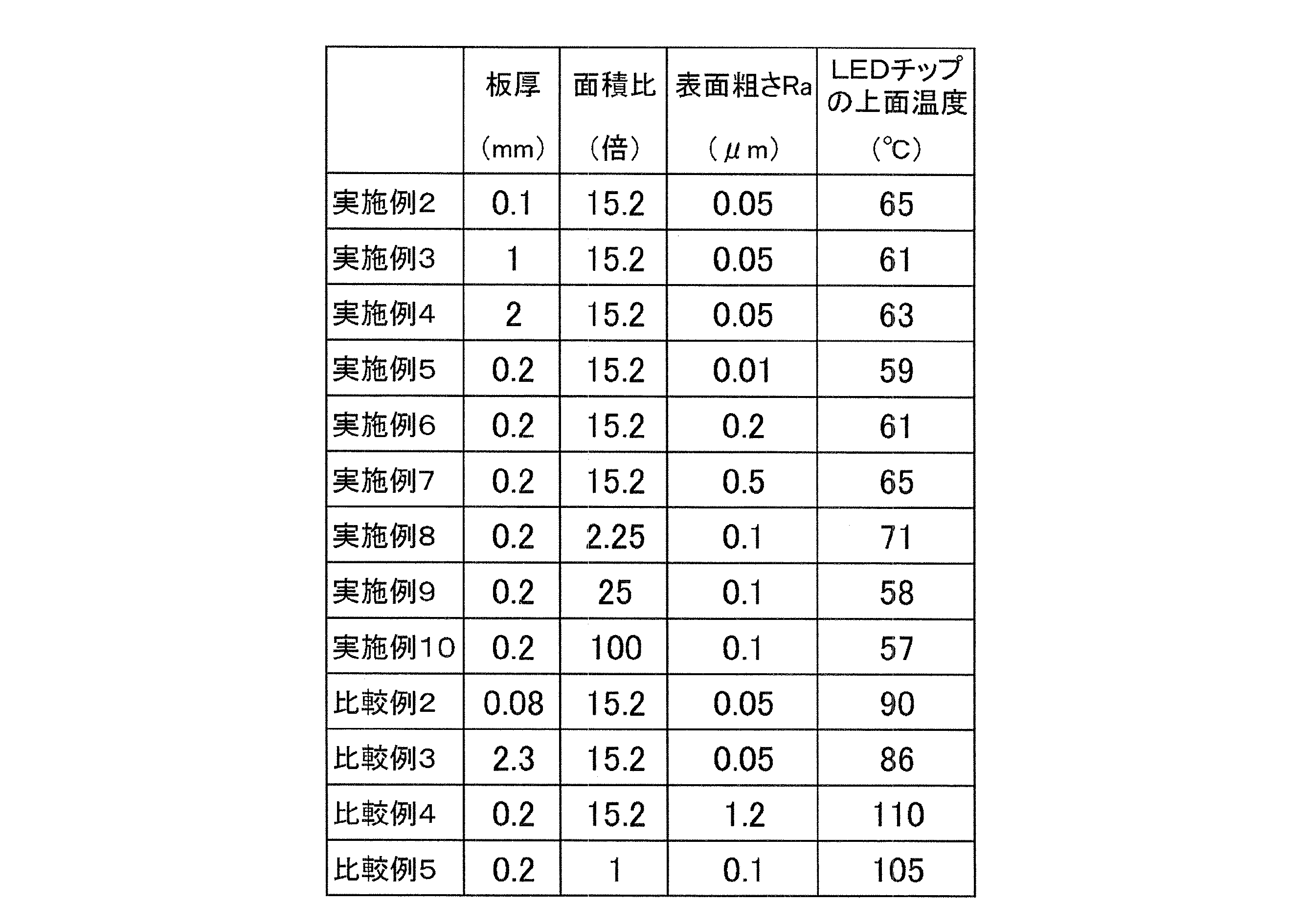
- the LED chip is directly mounted on the composite substrate using a bonding material, and the area of the LED chip mounting surface of the composite substrate is 2 with respect to the contact area with the LED chip. It is up to 100 times, preferably 2 to 25 times. If the area ratio (magnification) is less than twice, the heat from the LED chip cannot be sufficiently spread to the composite substrate, and the lighting temperature of the LED chip becomes high. On the other hand, when the area ratio (magnification) exceeds 100 times, an electrical joining member (for example, Au wire bonding) for energizing the LED chip becomes extremely long, and there is a concern that reliability may be lowered.
- an electrical joining member for example, Au wire bonding
- the “LED chip” refers to a structure composed of an LED element made of a III-V semiconductor crystal and a holding substrate.
- a III-V group semiconductor crystal emitting light in the ultraviolet to blue wavelength region is used, and specifically, InGaN, AlGaAs, AlGaInP, or the like.
- the holding substrate is a growth substrate used for epitaxial growth of a group III-V semiconductor crystal, or after a group III-V semiconductor crystal is epitaxially grown on the growth substrate, a high thermal conductivity substrate is bonded through a metal layer. Thereafter, the high thermal conductivity substrate from which the growth substrate has been removed. Examples thereof are sapphire, silicon carbide, silicon, Cu / W, Cu / Mo, and the like.
- the holding substrate belonging to the latter is used from the viewpoint of thermal conductivity, and the LED chip has a non-insulating structure.
- the advantage of the non-insulating LED chip is that high brightness can be obtained in a small area.
- the LED chip is directly mounted on the composite substrate using a bonding material.
- the joining is performed by, for example, soldering, brazing, a high thermal conductive adhesive, or the like, and preferably soldering or brazing.
- solder cream solder, eutectic solder, lead-free solder or the like can be used.
- a brazing method using a eutectic metal layer on the back surface of the LED chip is preferable, whereby the thickness of the layer made of the bonding material, that is, the bonding layer can be reduced to 1 to 5 ⁇ m.
- the “high thermal conductive adhesive” is an adhesive having a thermal conductivity of 10 W / (m ⁇ K) or more, and examples thereof include an Ag paste, a high thermal conductive silicone adhesive, and an Ag-based conductive adhesive. it can.
- “joining” means that the LED chip and the composite substrate are bonded, and is used in the same concept as mounting.
- the thickness of the bonding layer is preferably 0.1 mm or less, and particularly preferably 0.05 mm or less. When the thickness of the bonding layer exceeds 0.1 mm, the thermal resistance increases.
- the adhesion rate that is, the ratio of the area of the bonding layer to the bottom area of the LED chip is preferably close to 1, but if it is 0.5 or more, preferably 0.8 or more, the heat generated by the LED chip can be comfortably combined. Can be communicated to.
- the surface roughness (Ra) of the composite substrate exceeds 0.5 ⁇ m, there is a risk that problems such as a decrease in the adhesion rate may occur. The smaller the surface roughness (Ra), the better.
- the lower limit is preferably 0.01 ⁇ m.
- Composite substrate refers to an inorganic molded body, preferably an inorganic molded body having a porosity of 10 to 50% by volume, particularly preferably a porosity of 20 to 35% by volume.
- An alloy contained as a component preferably an aluminum-silicon alloy having an aluminum content of 80 to 97% by mass, is impregnated by, for example, the method of Japanese Patent No. 3468358, or silicon or a silicon alloy is obtained by melt impregnation, for example, No.
- thermal conductivity at a temperature of 25 ° C. is 100 to 600 W / (m ⁇ K), preferably 100 to 300 W / (m ⁇ K), temperature is 25 ° C.
- a linear expansion coefficient at ⁇ 150 ° C. is 3 to 12 ⁇ 10 ⁇ 6 / K, preferably 4 to 9 ⁇ 10 ⁇ 6 / K, and a three-point bending strength is 50 to 500 MPa, preferably 50 to 400 MPa.
- the material of the inorganic molded body is preferably at least one selected from silicon carbide, aluminum nitride, silicon nitride, diamond and graphite.
- the proportion of voids (porosity) in the inorganic molded body is preferably 10 to 50% by volume, particularly preferably 20 to 35% by volume. If the porosity exceeds 50% by volume, the linear thermal expansion coefficient of the composite substrate becomes too large, and if it is less than 10% by volume, aluminum, silicon or an alloy containing them as a component cannot be sufficiently impregnated. In addition, the thermal conductivity may be reduced.
- the porosity can be adjusted by adjusting the particle size of inorganic components such as silicon carbide, aluminum nitride, silicon nitride, diamond, graphite, molding pressure, sintering conditions, and the like.
- the composite substrate used in the present invention has a function as a heat spreader that spreads the heat generated in the LED chip in the surface direction, a highly reliable LED package for high-power LEDs can be manufactured.
- the thermal conductivity of the composite substrate at a temperature of 25 ° C. is 100 to 600 W / (m ⁇ K).
- the thermal conductivity is less than 100 W / (m ⁇ K)
- the heat generated by the LED chip cannot be sufficiently dissipated, and particularly in a high-power LED, the temperature of the element rises and the luminous efficiency decreases, and the element lifetime associated therewith. There is a risk of decline.
- the upper limit of the thermal conductivity is set to 600 W / (m ⁇ K) because the composite substrate becomes expensive.
- the thermal conductivity can be increased or decreased depending on the type, blending amount, etc. of the raw material of the inorganic molded body.
- the difference in coefficient of thermal expansion between the III-V semiconductor crystal constituting the LED chip and the holding substrate is small. Further, since the composite substrate to which the LED chip is bonded is bonded to the metal circuit of the circuit board, the composite substrate has a function that can relieve the stress caused by the difference in thermal expansion coefficient between the LED chip and the circuit board. It is preferable. Therefore, the linear thermal expansion coefficient of the composite substrate at a temperature of 25 ° C. to 150 ° C. is 3 to 12 ⁇ 10 ⁇ 6 / K. If the coefficient of thermal expansion is other than this, there is a risk that warping will occur after mounting, the mounting part will peel off, or the LED chip will break in the worst case due to the difference in linear thermal expansion coefficient with the LED chip.
- the linear thermal expansion coefficient of the composite substrate can be increased or decreased depending on the composition ratio of aluminum, silicon or an alloy containing them as a component and the inorganic molded body.
- the composite substrate has a strength that can be sustained when the LED chip is mounted with a bonding material, and (b) the bonding surface is flat with no inclusions such as voids or foreign matters on the bonding surface. That is.
- the three-point bending strength of the composite substrate is set to 50 MPa or more.
- the upper limit is 500 MPa.
- the surface roughness (Ra) of the composite substrate may be 0.5 ⁇ m or less.
- the three-point bending strength can be increased or decreased depending on the material of the inorganic molded body, the particle size of the inorganic component, the porosity, etc., and the surface roughness (Ra) can be increased or decreased depending on the grain size of the abrasive grains used for processing. Can do.
- the thickness of the composite substrate is set to 0.1 to 2 mm from the viewpoint of improving the heat dissipation of the LED chip assembly and the handling property when mounting the LED chip.
- the thickness is preferably 0.1 to 1 mm.
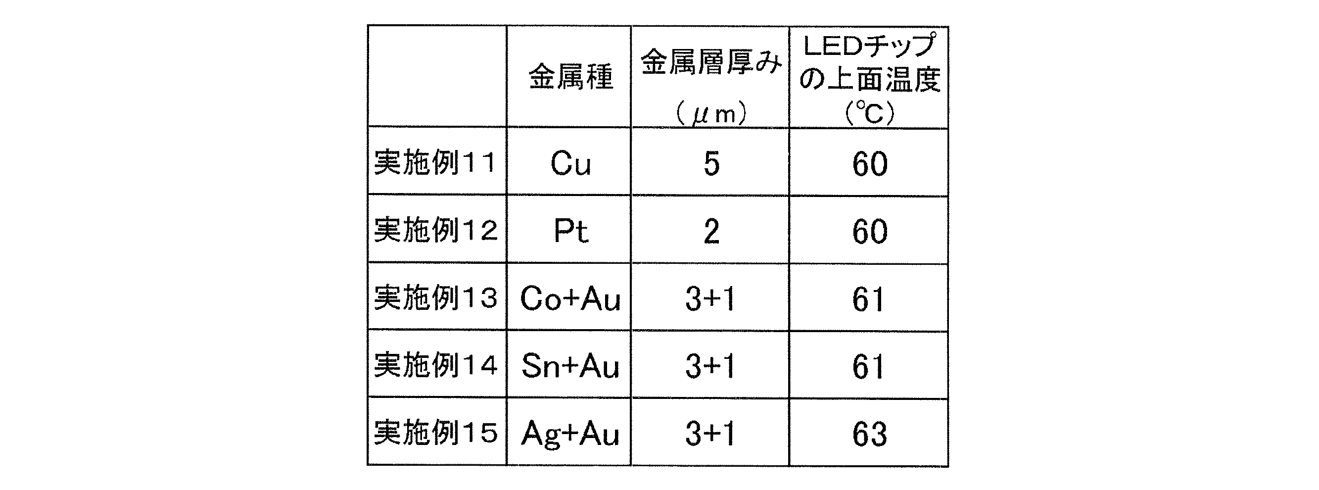
- the composite substrate has a metal layer having a thickness of 0.5 to 20 ⁇ m made of at least one metal selected from Ni, Co, Pd, Cu, Ag, Au, Pt and Sn, particularly preferably Ni or Au, on the surface. It is preferable to have.
- a particularly preferred metal layer thickness is 2 to 10 ⁇ m. This improves the adhesion rate. If the thickness of the metal layer is less than 0.5 ⁇ m, the effect of improving the adhesion rate is small, and if it exceeds 20 ⁇ m, there is a risk of peeling due to the difference in thermal expansion between the metal layer and the heat spreader.
- the metal layer can be formed by washing the composite substrate and then performing electroless plating or electrolytic plating with the above metal species. Besides the plating method, it can also be formed by a metal vapor deposition method or a metal coating method.
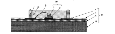
- ⁇ LED package> 1 to 3 are explanatory diagrams showing examples of LED packages.
- the LED package of the present invention has a basic structure in which the LED chip assembly 10 of the present invention is mounted on a circuit board 11, connected by an electrical connection member 9, and sealed by a resin sealing material 8 ( 1 to 3).
- An embodiment example using one LED chip assembly is shown in FIGS. 1 and 2, and an embodiment example using two or more LED chip assemblies is FIG. 3.
- An example using the dam material 7 is shown in FIGS. 1 and 3, and an example not using it is FIG. This will be described in more detail below.
- the LED chip assembly 10 of the present invention is mounted on a circuit board 11.
- the circuit board 11 is composed of a laminate of the metal circuit 3 and the metal substrate 5 with the insulating layer 4 interposed therebetween.
- the metal circuit 3 and the metal substrate 5 aluminum, iron, copper, or an alloy containing these metals as components is preferable.
- the surface of the metal substrate bonded to the insulating layer can be subjected to surface treatment such as sandblasting, etching, various plating treatments, and coupling agent treatment. .
- the thickness of the metal circuit is preferably 0.005 to 0.4 mm. If it is less than 0.005 mm, a sufficient conduction circuit as an LED package cannot be secured, and if it exceeds 0.40 mm, restrictions on circuit formation increase.
- the thickness of the metal substrate is preferably 0.1 to 4 mm. If it is too thin, the handleability is lowered. Even if it is too thick, there is not much practical advantage as an LED package for illumination.
- the insulating layer 4 is a cured product of a curable resin composition containing a heat-resistant resin, a curing agent, and an inorganic filler, and preferably has a thermal conductivity of 0.5 W / (m ⁇ K) or more. If the thermal conductivity is less than 0.5 W / (m ⁇ K), the heat generated by the LED chip cannot be sufficiently spread, so the junction temperature of the LED chip increases, the brightness of the LED chip decreases, and the lifetime There is a risk of lowering. An upper limit of thermal conductivity of 20 W / (m ⁇ K) is sufficient.
- the thickness of the insulating layer is preferably 30 to 200 ⁇ m. If it is less than 30 ⁇ m, the electrical insulation becomes insufficient, and if it exceeds 200 ⁇ m, the heat dissipation may be impaired.
- the heat-resistant resin for example, an epoxy resin, a silicone resin, a phenol resin, an imide resin, or the like can be used.
- the curing agent those described below are used.
- the inorganic filler include oxide ceramics such as aluminum oxide (alumina), silicon oxide, and magnesium oxide, nitride ceramics such as aluminum nitride, silicon nitride, and boron nitride, and carbide ceramics.
- the inorganic filler is preferably a spherical powder having a maximum particle size of 100 ⁇ m or less and a minimum particle size of 0.05 ⁇ m or more. Among them, those containing 50 to 75% by mass of particles having a particle size of 5 to 50 ⁇ m and 25 to 50% by mass of particles having a particle size of 0.2 to 1.5 ⁇ m are more preferable.
- the content of the inorganic filler in the insulating layer is preferably 70 to 95 parts by mass, particularly preferably 80 to 90 parts by mass with respect to 100 parts by mass of the total amount of the heat-resistant resin and the curing agent.
- the ratio of the inorganic filler exceeds 95 parts by mass with respect to 100 parts by mass of the total amount of the heat-resistant resin and the curing agent, the viscosity of the curable resin composition increases and the workability decreases. On the other hand, if it is less than 70 parts by mass, the thermal conductivity of the insulating layer may be lowered.
- a silane coupling agent, a titanate coupling agent, a stabilizer, a curing accelerator, and the like can be used as necessary.
- the storage elastic modulus of the insulating layer is preferably 15000 MPa or less at 300K in order to relieve the stress at the bonded portion.
- Such an insulating layer contains 5 to 50 parts by mass of a curing agent having a polyether skeleton and a primary amino group at the end of the main chain and 70 to 95 parts by mass of the inorganic filler per 100 parts by mass of the epoxy resin. This can be realized by preparing a cured curable resin composition.
- epoxy resin general-purpose epoxy resins such as bisphenol F type epoxy resin and bisphenol A type epoxy resin can be used.
- Epoxy resin having a dicyclopentadiene skeleton, epoxy resin having a naphthalene skeleton, epoxy having a biphenyl skeleton When the resin contains 10% by mass or more of one or more selected from epoxy resins having a novolac skeleton in the epoxy resin, the balance between stress relaxation and moisture resistance is further improved.
- Typical epoxy resins having a novolak skeleton include a phenol novolak type epoxy resin and a cresol novolak type epoxy resin, but an epoxy resin having a dicyclopentadiene skeleton, a naphthalene skeleton, or a biphenyl skeleton and a novolak skeleton can also be used.
- the epoxy resin an epoxy resin having the above skeleton may be used alone.
- a thermosetting resin such as a phenol resin or a polyimide resin, or a high molecular weight resin such as phenoxy resin, acrylic rubber, or acrylonitrile-butadiene may be blended as another resin mainly composed of an epoxy resin.
- the blending amount of the high molecular weight resin is preferably 30% by mass or less with respect to the total amount with the epoxy resin.
- the curing agent has a polyether skeleton, and a curing agent having a primary amino group at the end of the main chain is used to reduce the storage elastic modulus of the resin composition after curing. It can also be used in combination with other curing agents. When an aromatic amine curing agent is used in combination, the balance of stress relaxation, electrical insulation, moisture resistance and the like can be further improved.
- the aromatic amine curing agent diaminodiphenylmethane, diaminodiphenylsulfone, metaphenylenediamine and the like can be used.
- a curing agent such as a phenol novolac resin can be further used in combination.
- a curable resin composition slurry for forming an insulating layer is pattern-printed on a metal substrate 5 (for example, an aluminum substrate) by a method such as screen printing and heated to be in a semi-cured state, and then a metal circuit 3 is formed.
- a metal foil for example, a copper foil
- the insulating layer is processed into a semi-cured sheet in advance, and the metal circuit 3 is formed by a hot press apparatus. And a method of integrating with a metal foil (for example, a copper foil).
- a method for forming a pattern of a metal circuit for example, a method in which a resist layer is applied in advance to a predetermined position on a metal foil and cured, and then etched using an etchant such as cupric chloride, a mixture of hydrogen peroxide and sulfuric acid, or the like is used. It is done.
- an etchant such as cupric chloride, a mixture of hydrogen peroxide and sulfuric acid, or the like
- the LED chip 1 of the LED chip assembly and the metal circuit 3 of the circuit board are connected by an electrical connection member 9.
- the electrical connection member 9 for example, wire bonding using Ag, Au or the like, a bump, a bridge, or the like is used.
- the LED chip joined body 10 is joined to the metal circuit 3, and the above-described soldering, brazing, high thermal conductive adhesive, or the like is used for the joining. Preferably, it is soldering.
- ⁇ LED package-resin sealing material> In the LED package of the present invention, at least the LED chip assembly 10 and the electrical connection member 9 are sealed with a resin sealing material 8 containing a fluorescent material.
- a resin sealing material 8 containing a fluorescent material In resin sealing, as shown in FIGS. 1 and 3, in order to suppress the spread of the resin sealing material, the dam material 7 can be installed so as to surround the outer periphery of the LED chip assembly.
- the dam material can be formed by screen printing, a dispenser, or the like using, for example, a silicone resin or an epoxy resin.
- thermosetting resins such as silicone resin, epoxy resin, polydimethylsiloxane derivative having epoxy group, oxetane resin, acrylic resin, cycloolefin resin, etc. are used, but higher refractive index and heat resistance. From the viewpoint of imparting properties, a silicone resin is preferable.
- the resin sealing material contains a fluorescent substance, and its content is preferably 1 to 50% by mass.
- the fluorescent material is not particularly limited as long as it receives visible light from the LED chip.
- ⁇ -type sialon, ⁇ -type sialon, CASIN (Ca ⁇ Al ⁇ Si ⁇ N 3 ), yttrium ⁇ aluminum ⁇ garnet, sulfide, etc. and at least one of them is used.
- ⁇ -type sialon and ⁇ -type sialon are preferable.
- the ⁇ -type sialon does not need to be a special one, and a commonly available one is used.
- the oxygen content is preferably 1.2% by mass or less.
- a cumulative particle size (D10) with a cumulative value of 10% by volume is 2 to 15 ⁇ m.
- a particle size (D50) having a value of 50% by volume of 5 to 20 ⁇ m and a cumulative value of 90% by volume of a particle size D90) of 6 to 50 ⁇ m are preferred because higher luminance can be achieved.
- the resin sealing material preferably contains a filler having a relative refractive index of 2.2 or more.
- a filler having a relative refractive index of 2.2 or more.
- Illustrative examples include titanium oxide, zirconium oxide, and potassium titanate.
- the average particle diameter of the filler is preferably 100 nm or less. If it exceeds 100 nm, the amount of light scattering loss may increase.
- the resist layer 6 By disposing the resist layer 6 in the LED package of the present invention, the light from the LED chip can be more efficiently irradiated on the front surface.
- the resist layer should not be disposed between the light emitting portion of the LED chip and the electrical connection member so as not to inhibit the light emission of the LED chip.
- the reflectance of the resist layer is preferably 70% or more with respect to light having a wavelength of 400 to 800 nm, more preferably the maximum value of the reflectance in each wavelength range of 450 to 470 nm, 520 to 570 nm, and 620 to 660 nm. , Both are 80% or more, and further 85% or more.
- the resist layer having the above characteristics can be produced by adding a white pigment to a curable resin containing one or both of an ultraviolet curable resin and a thermosetting resin.
- a curable resin an epoxy resin, an acrylic resin, and a mixture thereof are preferably used.
- the white pigment at least one selected from zinc oxide, calcium carbonate, titanium dioxide, alumina, and smectite is used. Of these, rutile type titanium dioxide is preferable because of its weak photocatalytic action.
- the white pigment may have been subjected to a surface treatment with, for example, silicon dioxide, aluminum hydroxide or the like to weaken the photocatalytic action.
- the content of the white pigment is too small, a sufficient reflection effect cannot be obtained. If the content is too large, the fluidity at the time of film formation decreases and a uniform film cannot be formed. It is preferably 30 to 70% by volume, more preferably 30 to 60% by volume.
- the LED package of the present invention can be provided with a reflector (not shown) in order to more efficiently irradiate the front surface with light from the LED chip.
- a reflector not only a separate reflector but also a counterbore having a conical shape, a dome shape or the like can be formed on a metal substrate directly under the LED chip joined body to make the insulating layer itself a reflector.
- a separate reflector for example, a metal such as Ag, Al, Ni, Au, Cu, SiO 2 / ZrO 2 , SiO 2 / TiO, etc., on the inner surface of a cylindrical body having an inclination such as glass, ceramics, metal, or resin A metal oxide film reflecting layer formed of 2 or the like can be used.
- the manufacturing method of the LED package according to the present invention includes the steps (i) to (vi) described above.
- description will be made while avoiding duplication with the above description as much as possible.
- an inorganic molded body to be impregnated with aluminum or aluminum alloy, silicon or silicon alloy is manufactured.
- the inorganic molded body (hereinafter also referred to as “preform”) includes a sintered body having a porosity of 10 to 50% by volume (hereinafter also referred to as “inorganic porous body”) and a porosity of 10 to 50 volume. % Powder compact.
- a part or all of the voids of the preform is impregnated with aluminum or an aluminum alloy, or silicon or a silicon alloy, so that a composite substrate having the above characteristics is obtained.
- the porosity of the preform can be adjusted by adjusting the particle size of the raw material powder, molding pressure, heat treatment conditions, and the like.
- the preform powder molding is molded by using the raw material powder alone or in combination with an inorganic binder such as silica sol or alumina sol.
- an inorganic binder such as silica sol or alumina sol.
- a general ceramic powder forming method such as press forming or cast forming is employed.
- the inorganic porous body of the preform can be produced by, for example, sintering the powder molded body.
- Step> the preform is impregnated with aluminum or an aluminum alloy by a molten metal forging method or impregnated with silicon or a silicon alloy by a melt impregnation method to produce a composite.
- the molten metal forging method aluminum or an aluminum alloy is heated to a melting point or higher, and the preform is pressure impregnated into the preform.
- An example of the specific conditions of the molten metal forging method is described in the above-mentioned patent document, and these can also be adopted in the present invention, and further described as follows. According to the molten metal forging method, a composite substrate having a large thermal conductivity and excellent heat dissipation can be obtained.
- the composition of aluminum or aluminum alloy used in the molten metal forging method preferably contains 70% by mass or more of aluminum.
- the thermal conductivity of the composite substrate may be reduced.
- the aluminum alloy include aluminum-silicon and aluminum-silicon-magnesium.
- an aluminum alloy containing 3 to 20% by mass of silicon having a low melting point so as to sufficiently penetrate into the voids of the preform is preferable.
- an aluminum-silicon-magnesium alloy containing up to 3% by mass of magnesium is more preferable because the bond between the ceramic and the metal portion becomes stronger.
- the metal components other than aluminum, silicon, and magnesium in the aluminum alloy are not particularly limited as long as the characteristics do not change extremely, and for example, copper or the like may be included.
- the preforms are preferably impregnated by connecting a plurality of preforms to form a laminate. It is preferable to sandwich a release plate such as a stainless steel plate or a ceramic plate with a release agent applied to the plurality of connections, and a jig such as an iron or graphite bolt and nut is used to fix the preform. It is preferable to use it.
- a release plate such as a stainless steel plate or a ceramic plate with a release agent applied to the plurality of connections
- a jig such as an iron or graphite bolt and nut is used to fix the preform. It is preferable to use it.
- sprays containing release agent powders such as graphite, boron nitride, and alumina are used.
- the laminate After the laminate is heated at a temperature of about 600 to 800 ° C., one or two or more pieces are placed in the container, and then the molten aluminum or aluminum alloy heated to the melting point or higher is quickly supplied, and 30 MPa or more, In particular, it is preferable to pressurize at a pressure of 50 MPa or more. As a result, aluminum or an aluminum alloy is easily impregnated into the voids of the preform.
- the heating temperature of the laminate exceeds 800 ° C., the raw material powder used for forming the preform may be oxidized, and the thermal conductivity and the like may be reduced. Thereafter, the impregnated product is annealed as necessary to remove distortion during impregnation.
- silicon or a silicon alloy and a preform are placed in a crucible made of, for example, graphite or BN and heat-treated at a temperature equal to or higher than the melting point of silicon or the silicon alloy in a non-oxidizing atmosphere or reduced pressure.
- the preform is impregnated with silicon or a silicon alloy by the pressure impregnation method.
- powder metallurgy can be used for the composite of the preform and silicon or silicon alloy
- the non-pressure impregnation method is preferred from the standpoint of characteristics.
- An example of specific conditions of the melt impregnation method is described in the above-mentioned patent document, and these can be employed in the present invention.
- the melt impregnation method it becomes easy to impregnate a metal having a low viscosity of the molten metal, such as silicon or a silicon alloy.
- the silicon alloy to be impregnated is preferably a silicon alloy containing 70% by mass or more of silicon in order to make the molten metal low in viscosity and easily penetrate into the preform.
- Step> the composite is processed into a pre-composite substrate having a plate thickness of 0.1 to 2 mm and a surface roughness (Ra) of 0.5 ⁇ m or less.
- the thermal expansion coefficient is 10 to 50% by volume of aluminum or aluminum alloy, or silicon or silicon alloy
- the thermal conductivity at 25 ° C. is 100 to 600 W / (m ⁇ K)
- the linear expansion coefficient is 25 to 150 ° C. Is 3 to 12 ⁇ 10 ⁇ 6 / K
- a pre-composite substrate having a three-point bending strength of 50 to 400 MPa is manufactured.
- the content of aluminum or aluminum alloy, or silicon or silicon alloy is adjusted, and the thermal conductivity and linear expansion coefficient are controlled.
- the content of aluminum or aluminum alloy, or silicon or silicon alloy in the pre-composite substrate is preferably 20 to 35% by volume.
- the composite is preferably processed as follows.
- the shape of the composite is a cylinder
- a processing machine such as a double-side grinding machine, a rotary grinding machine, a surface grinding machine, or a lapping machine.
- the thickness is 0.1 to 2 mm and the surface roughness (Ra) is 0 with a processing machine such as a double-sided grinder, rotary grinder, surface grinder, or lapping machine. Process to 5 ⁇ m or less.
- the pre-composite substrate is cut to an area of 2 to 100 times the contact area of the LED chip (that is, the bottom area of the LED chip), and the composite substrate 2 is manufactured. Thereafter, one or two or more LED chips 1 are mounted with a bonding material, and the LED chip bonded body 10 is manufactured. In this step, cutting to an area of 2 to 100 times, and forming a metal layer of at least one metal selected from Ni, Co, Pd, Cu, Ag, Au, Pt and Sn as necessary. Details of what can be done are described above.
- the peripheral processing of the pre-composite substrate can be performed by dicing, laser processing, water jet processing, and electric discharge processing. Dicing is optimal in terms of processing accuracy and processing speed, and laser processing is most excellent in terms of processing speed.
- the number of LED chips to be mounted on the composite substrate is limited as long as the area of the composite substrate is 2 to 100 times the adhesion area of the LED chip, and the layout does not hinder the mounting and heat dissipation of individual LED chips. There is no. For this reason, it can also be set as the LED chip assembly which attached two or more LED chips to one composite substrate.
- An advantage of mounting a plurality of LED chips is that man-hours in the mounting process can be reduced.
- Example 1 ⁇ Pre-composite substrates A and B using an inorganic porous material> Silicon carbide powder A (commercial product: average particle size 200 ⁇ m) 1800 g, silicon carbide powder B (commercial product: average particle size 20 ⁇ m) 900 g, silicon carbide powder C (commercial product: average particle size 2 ⁇ m) 300 g, and molded binder (methylcellulose) 150 g of trade name “Metroze” manufactured by Shin-Etsu Chemical Co., Ltd.) was weighed and mixed with a stirring mixer for 30 minutes.
- a linear expansion coefficient measurement specimen (diameter 3 mm, length 10 mm) and a thermal conductivity measurement specimen (25 mm ⁇ 25 mm ⁇ 1 mm) were cut out by grinding, and a wire having a temperature of 25 ° C. to 150 ° C.
- the coefficient of expansion was measured with a thermal dilatometer (Seiko Denshi Kogyo Co., Ltd .; TMA300), the thermal conductivity at a temperature of 25 ° C. was measured with a laser flash method (manufactured by ULVAC; TC3000), and the three-point bending strength was measured with a bending strength tester.
- the linear expansion coefficient was 5.0 ⁇ 10 ⁇ 6 / K
- the thermal conductivity was 250 W / (m ⁇ K)
- the strength was 350 MPa.
- the composite was processed into a cylindrical shape having a diameter of 50.8 mm and a height of 100 mm using a diamond grinder with a cylindrical grinder, and then a diamond abrasive grain was used with a multi-wire saw, and the cutting speed was 0.2 mm. / Min. And cut into a disk shape having a plate thickness of 0.3 mm, and further ground to a plate thickness of 0.22 mm with a double-side grinding machine using a # 600 diamond grindstone. Thereafter, polishing was performed to a thickness of 0.2 mm using diamond abrasive grains on a lapping machine, and then ultrasonic cleaning was performed in pure water and then in isopropyl alcohol, followed by drying to produce a pre-composite substrate A. . This surface roughness (Ra) was 0.05 ⁇ m.
- the pre-composite substrate A was subjected to electroless Ni—P plating and electro Au plating to form a metal layer (5 ⁇ m thickness) of (Ni—P: 4 ⁇ m + Au: 1 ⁇ m).
- the surface roughness (Ra) was 0.1 ⁇ m.
- a commercially available ultraviolet curable solder resist layer was applied to one side of the pre-composite substrate provided with the metal layer with a screen printer, and then cured with an ultraviolet ray to form a resist layer (15 ⁇ m) (not shown) of 4 mm.
- a pre-composite substrate B was formed at intervals.
- the LED package shown in FIG. 1 was manufactured using the following constituent materials. That is, the insulating layer 4 is laminated on the metal substrate 5 to a thickness of 80 ⁇ m, and then the metal foil is laminated, the metal circuit 3 is formed by chemical etching, and the resist layer 6 is applied to the surface of the circuit board 11. Manufactured. On the other hand, the LED chip 1 was bonded to the composite substrate 2. For the bonding of A and a composite substrates, an Ag paste high thermal conductive adhesive (Kyocera Chemical Co., Ltd .: CT284R) is used. For the composite substrates of B and b, a cream solder adhesive is used for the metal layer between the resist layers. It was. 120 LED chip assemblies 10 were produced for each.
- the LED chip assembly was mounted on the circuit board 11 by wire bonding using cream solder and the electrical connection member 9.
- the area of the LED chip mounting surface of the obtained LED chip assembly was 15.2 times the bottom area of the LED chip.
- the dam material 7 was provided and the resin sealing material 8 was filled, and the LED package of this invention was manufactured.
- LED chip 1 (manufactured by Cree: EZ1000 shape: 1 mm ⁇ 1 mm ⁇ 0.1 mm output: 3 W)
- Composite substrate 2 Composite substrate A, B, a or b manufactured above
- Metal circuit 3 Copper insulating layer having a thickness of 35 ⁇ m 4: Bisphenol A type epoxy resin (manufactured by Japan Epoxy Resin, “EP-828”) and a curing agent phenol novolac (manufactured by Dainippon Ink & Chemicals, “TD-2131”) ))
- an inorganic filler crushed silica powder having an average particle size of 1.2 ⁇ m (manufactured by Tatsumori Co., Ltd., “A-1”): crushed silica powder having an average particle size of 10 ⁇ m (manufactured by Tatsumori Co., Ltd., “5X”)
- Resist layer 6 (Taiyo Ink, “PSR4000LEW1”)
- Dam material 7 Silicone resin (manufactured by Shin-Etsu Chemical Co., Ltd., “KER-2000-DAM”)
- Resin sealing material 8 80% by mass of a silicone resin (Toray Dow Corning, “JCR6125”) and 20% by mass of ⁇ -sialon (D10 is 4.8 ⁇ m, D50 is 9.1 ⁇ m, D90 is 18.9 ⁇ m) blend.
- Electrical connection member 9 gold wire.
- the upper surface temperature of the LED chip of the LED package manufactured using the composite substrate A, the composite substrate B, the composite substrate a, and the composite substrate b is 69 ° C., 60 ° C., 70 ° C., respectively, with an average value of 5 pieces. It was 61 ° C.
- Comparative Example 1 In the LED package of Example 1 using the composite substrate B, the LED chip was mounted directly on the circuit board using cream solder without producing the LED chip assembly, and the upper surface temperature of the LED chip was 105 ° C. there were.
- Example 11-15 The composite substrate B of Example 1 was formed except that a metal layer having the metal species and metal layer thickness shown in Table 2 was formed instead of the plating layer (5 ⁇ m thickness) of (Ni—P: 4 ⁇ m + Au: 1 ⁇ m). An LED package was manufactured in the same manner as used, and the upper surface temperature of the LED chip was measured. The results are shown in Table 2.
- Example 16 ⁇ LED chip assembly and LED package using composite substrates C and D using an inorganic porous body> 1300 g of silicon carbide powder D (commercial product: average particle size 150 ⁇ m), 700 g of silicon carbide powder E (commercial product: average particle size 10 ⁇ m), and 300 g of silica sol (Nissan Chemical Co., Ltd .: Snowtex) were weighed and stirred. After mixing for 30 minutes, it was press-molded into a plate having dimensions of 160 mm ⁇ 160 mm ⁇ 5 mm at a surface pressure of 30 MPa to produce a molded body. The obtained molded body was dried at a temperature of 120 ° C. for 1 hour, and then fired in a nitrogen atmosphere at a temperature of 1400 ° C.
- Ten inorganic porous bodies are formed into a structure (170 mm ⁇ 170 mm ⁇ 40 mm) with a release plate (160 mm ⁇ 160 mm ⁇ 0.8 mm) coated with a graphite release agent on each sheet, and iron plates ( A plate thickness of 12 mm) was arranged and connected with eight bolts to form one laminate.
- a composite 155 mm ⁇ 155 mm ⁇ 3 mm was produced in the same manner as the composite substrate A of Example 1, the thermal expansion coefficient at a temperature of 25 ° C. to 150 ° C., the thermal conductivity at a temperature of 25 ° C., and the three-point bending strength. Were measured to be 7.5 ⁇ 10 ⁇ 6 / K, 200 W / (m ⁇ K), and 400 MPa, respectively.
- the obtained composite was surface-processed into a plate thickness of 0.4 mm using a diamond grindstone with a surface grinder, and then a water jet processing machine (Abstract Jet Cutter NC manufactured by Sugino Machine) was used. Then, using a garnet having a particle size of 100 ⁇ m as abrasive grains under the conditions of a pressure of 250 MPa and a processing speed of 100 mm / min, it was cut into a shape having a diameter of 50.8 mm ⁇ 0.4 mm.
- the upper surface temperature of the LED chip of the LED package manufactured using the composite substrate C and the upper surface temperature of the LED chip of the LED package manufactured using the composite substrate D were measured. And 62 ° C.
- Example 17 ⁇ LED chip assembly and LED package using composite substrates E and F using an inorganic porous body>
- a stainless steel plate using an isotropic graphite molded body manufactured by Tokai Carbon Co., Ltd .: G458, porosity: 13% by volume, dimensions: 100 mm ⁇ 100 mm ⁇ 100 mm) as an inorganic porous body, and a graphite release material applied as a release plate A composite was manufactured according to the manufacture of the composite substrate A, except that (100 mm ⁇ 100 mm ⁇ 0.8 mm) was used.
- a metal layer similar to that of the pre-composite substrate B is applied to the pre-composite substrate E to obtain a pre-composite substrate F, and then the obtained pre-composite substrates E and F are cut at a cutting speed of 0.5 mm using an electric discharge machine.
- the composite substrates E and F were manufactured by cutting into a shape of 3.9 mm ⁇ 3.9 mm at / s.
- the LED chips (CREE: EZ1000 / 1 mm ⁇ 1 mm ⁇ 0.1 mm) with an output of 3 W are joined to the composite substrates E and F with cream solder, the upper surface of the LED chip of the LED package manufactured using the composite substrate E When the temperature and the upper surface temperature of the LED chip of the LED package manufactured using the composite substrate F were measured, they were 72 ° C. and 66 ° C., respectively.
- Example 18 ⁇ LED chip assembly and LED package using composite substrates G and H using an inorganic porous body> A mixed powder of 2880 g of aluminum nitride powder (commercial product: average particle size 2 ⁇ m), 120 g of yttria powder (commercial product: average particle size 1 ⁇ m), 150 g of molding binder (methylcellulose), and 150 g of pure water was press-molded at a surface pressure of 10 MPa. Thereafter, CIP molding was further performed at a molding pressure of 100 MPa to produce a cylindrical body (diameter 55 mm ⁇ 110 mm). This was degreased at a temperature of 600 ° C. for 2 hours in an air atmosphere, then fired at a temperature of 1780 ° C. for 4 hours in a nitrogen atmosphere to produce a sintered body, and then the porosity was 22 using a diamond grindstone at a machining center. % Inorganic porous material (diameter 52 mm ⁇ 100 mm) was produced.
- a pre-composite substrate G (diameter 50.8 mm ⁇ 0.2 mm) was prepared in the same manner as the composite substrate A of Example 1 except that this inorganic porous material was used and that pure aluminum was used instead of the aluminum alloy. Manufactured. The surface roughness (Ra) was 0.06 ⁇ m. Further, a metal layer similar to that of the pre-composite substrate B is applied to the pre-composite substrate G to obtain a pre-composite substrate H, and then the obtained pre-composite substrates G and H are cut with a laser processing machine at a cutting speed of 8 mm / s. Were cut into a shape of 3.9 mm ⁇ 3.9 mm to produce composite substrates G and H.
- LED chips (CREE: EZ700 / 0.7 mm ⁇ 0.7 mm ⁇ 0.1 mm) with an output of 1 W are bonded to the composite substrates G and H with a solder paste adhesive at 2 mm intervals to form an LED chip assembly.
- the obtained LED chip assembly has a structure in which four LED chips are mounted on the upper surface of one composite substrate, and the area of the LED chip mounting surface of the composite substrate is the total of the bottom area of the LED chips. It was 7.8 times. A voltage was applied to the LED chip so that the output was 4 W, and the temperature of the upper surface of the LED chip was measured by infrared thermography. As a result, the upper surface temperature of the LED chip of the LED package manufactured using the composite substrate G was 70, and that manufactured using the composite substrate H was 63 ° C.
- Example 19 ⁇ LED chip assembly and LED package using composite substrates I and J using inorganic porous material> Except for using a mixture of 2790 g of silicon nitride powder (commercial product: average particle size 1 ⁇ m), 150 g of yttria powder (commercial product: average particle size 1 ⁇ m), and 60 g of magnesium oxide powder (commercial product: average particle size 1 ⁇ m), A cylindrical body (diameter 55 mm ⁇ 110 mm) was produced in the same manner as in Example 18. This was fired for 4 hours at a temperature of 1880 ° C.
- Example 20 ⁇ LED chip assembly and LED package using composite substrates c and d using inorganic powder compacts> 7 g of diamond powder A (Diamond Innovations, MBG-600, average particle size: 120 ⁇ m) and 3 g of diamond powder B (Diamond Innovations, MBG-600, average particle size: 15 ⁇ m) in an alumina mortar After mixing for a minute, a graphite jig Y having an outer diameter of 52.4 mm ⁇ 9 mm was inserted into a cylindrical graphite jig X having an outer dimension of 70 mm ⁇ 70 mm ⁇ 20 mm (inner diameter: diameter 52.5 mm ⁇ 20 mm). Thereafter, 10 g of diamond mixed powder was filled, and a graphite jig Y was further inserted on the upper surface of the diamond mixed powder to produce an inorganic powder molded body having a porosity of 35%.
- diamond powder A Diamond Innovations, MBG-600, average particle size: 120 ⁇ m
- This inorganic powder compact was subjected to impregnation treatment with a laminate according to the production of the composite substrate a to produce a composite (70 mm ⁇ 70 mm ⁇ 20 mm) surrounded by a cylindrical graphite jig.
- This was ground into a plate-like body (70 mm ⁇ 70 mm ⁇ 1 mm) from both main surface sides (70 mm ⁇ 70 mm) using a diamond grinder with a surface grinder until the composite was exposed.
- the outer peripheral process was carried out in the disk (diameter 50.8 mm x 1 mm) shape with the water jet processing machine, and the composite substrate c was manufactured.
- This surface roughness (Ra) was 0.4 ⁇ m.
- a composite substrate d was manufactured by applying a plating layer and a resist layer in the same manner as the composite substrate b.
- the thermal conductivity of the composite substrate c at a temperature of 25 ° C. was 500 W / (m ⁇ K).
- the upper surface temperature of the LED chip of the LED package manufactured using the composite substrate c was 66 ° C.
- that manufactured using the composite substrate d was 58 ° C.
- Example 21 ⁇ LED chip assembly and LED package using composite substrates K and L using inorganic porous material>
- An inorganic porous material (outer dimension: diameter 52 mm ⁇ height 100 mm, porosity: 20%) manufactured in the manufacturing process of the composite substrate A of Example 1 was used with a diamond grindstone at a machining center, and the outer dimension was 52 mm ⁇ 20 mm in diameter. Processed into a disk. This disk and lump silicon were put in a graphite crucible coated with BN powder and set in an electric furnace. The furnace was evacuated and held at 1650 ° C. for 8 hours to impregnate the disc with silicon.
- Example 2 After cooling to room temperature, excess silicon was removed with a cylindrical grinder to produce a composite, and in the same manner as in Example 1, the linear expansion coefficient at a temperature of 25 ° C. to 150 ° C. and the thermal conductivity at a temperature of 25 ° C. was measured, the coefficient of linear expansion was 4.3 ⁇ 10 ⁇ 6 / K, and the thermal conductivity was 210 W / (m ⁇ K).
- the same processing as that of the composite substrate A was performed to manufacture the composite substrate K, and the same processing as that of the composite substrate B was performed to manufacture the composite substrate L.
- the surface roughness (Ra) of the composite substrate K was 0.08 ⁇ m.
- the upper surface temperature of the LED chip of the LED package manufactured using the composite substrate K was 69 ° C.
- that manufactured using the composite substrate L was 61 ° C.
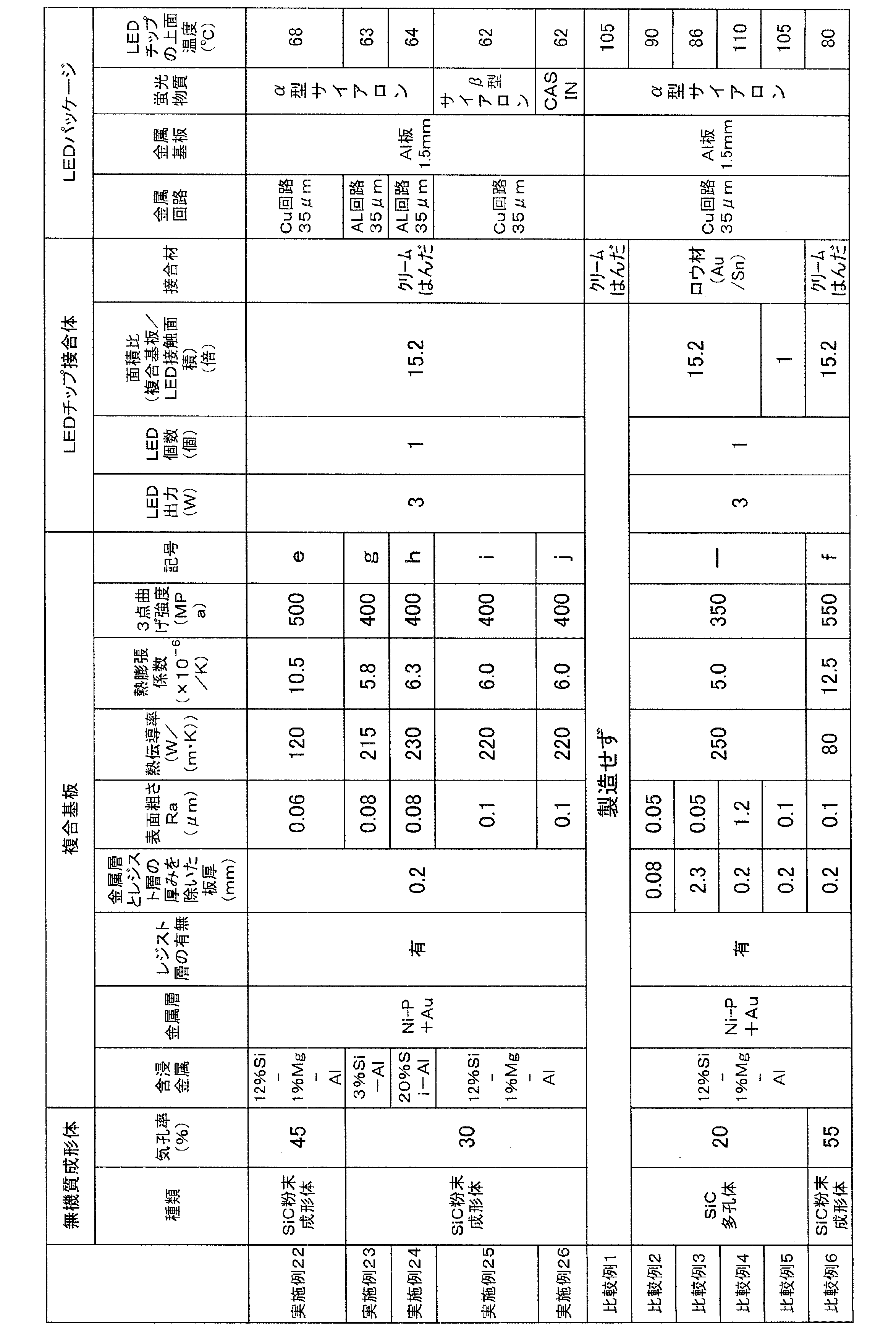
- Example 22 Comparative Example 6 ⁇ LED chip bonded body and LED package using composite substrate e, f using inorganic powder molded body> 461 g (Example 22) of silicon carbide powder E (commercial product: average particle diameter 10 ⁇ m), or 377 g (comparative example 6) of silicon carbide powder F (commercial product: average particle diameter 6 ⁇ m) were transferred to a cylindrical graphite jig ( External dimensions: 70 mm ⁇ 70 mm ⁇ 110 mm, inner dimensions: diameter 55 mm ⁇ height 110 mm), press-molded with a surface pressure of 5 MPa, porosity of 45% (Example 22) or porosity of 55% (comparison) The powder compact of Example 6) (a cylindrical body having a diameter of 55 mm and a height of 110 mm) was produced.
- the composite substrate e (Example 22) and composite substrate f (Comparative Example 6) were manufactured in the same manner as in the case of the composite substrate b of Example 1, and the LED chip assembly was manufactured. The LED package was manufactured and the upper surface temperature of the LED chip was measured. The results are shown in Table 3. Further, in the same manner as in Example 1, when the linear expansion coefficient at a temperature of 25 ° C. to 150 ° C., the thermal conductivity at a temperature of 25 ° C., and the three-point bending strength were measured, the linear expansion coefficient of the composite substrate e was 10.5.
- thermal conductivity 120 W / (m ⁇ K)
- strength 500 MPa
- the linear expansion coefficient of the composite substrate f is 12.5 ⁇ 10 ⁇ 6 / K
- thermal conductivity 80 W / (m ⁇ K). K)
- the strength was 550 MPa.
- Examples 23 and 24 ⁇ LED chip bonded body and LED package using composite substrate g, h using inorganic powder molded body> Instead of an aluminum alloy containing 12% by mass of silicon and 1% by mass of magnesium, an aluminum alloy containing 3% by mass of silicon (Example 23) or an aluminum alloy containing 20% by mass of silicon (Example 24) was used. And the composite substrate g and composite substrate in the same manner as the composite substrate b of Example 1 except that an aluminum (Al) circuit (thickness 35 ⁇ m) was used instead of the copper (Cu) circuit (thickness 35 ⁇ m). The LED package was manufactured via the manufacture of h and the manufacture of the LED chip assembly, and the upper surface temperature of the LED chip was measured. The results are shown in Table 3.
- the linear expansion coefficient at a temperature of 25 ° C. to 150 ° C. and the thermal conductivity at a temperature of 25 ° C. were measured in the same manner as in Example 1, the linear expansion coefficient of the composite substrate g was 5.8 ⁇ 10 ⁇ 6 / K, the thermal conductivity was 215 W / (m ⁇ K), the linear expansion coefficient of the composite substrate h was 6.3 ⁇ 10 ⁇ 6 / K, and the thermal conductivity was 230 W / (m ⁇ K).
- Examples 25 and 26 ⁇ LED chip assembly and LED package with composite substrate i, j using inorganic powder compact>
- the composite substrate i (Example 25) is the same as the composite substrate b of Example 1 except that ⁇ -type sialon powder (Example 25) or CASIN powder (Example 26) is used instead of the ⁇ -type sialon powder.
- the composite substrate j (Example 26) was manufactured, and the LED packages were manufactured via the manufacture of the LED chip assembly. When the upper surface temperature of the LED chip was measured, all of the results were as good as those of the LED package manufactured using the composite substrate b of Example 1.
Abstract
Description
(i)炭化珪素、窒化アルミニウム、窒化珪素、ダイヤモンド及び黒鉛から選ばれた少なくとも1種を用いて、気孔率が10~50体積%の焼結体又は粉末成形体からなる無機質成形体を製造する工程
(ii)上記無機質成形体に、溶湯鍛造法によりアルミニウム又はアルミニウム合金を含浸させるか、又は溶融含浸法によりシリコン又はシリコン合金を含浸させて複合体を製造する工程
(iii)上記複合体を加工して、板厚が0.1~2mm、表面粗さ(Ra)が0.5μm以下で、しかも温度25℃の熱伝導率が100~600W/(m・K)、温度25℃~150℃の線膨張係数が3~12×10-6/K、3点曲げ強度が50~400MPaであるプレ複合基板を製造する工程
(iv)上記プレ複合基板に、必要に応じて、Ni、Co、Pd、Cu、Ag、Au、Pt及びSnから選ばれた少なくとも1種の金属による金属層を形成させてから、実装されるLEDチップの接触面積の2~100倍の面積となるように切断して複合基板を製造した後、接合材によって一個又は二個以上のLEDチップを実装し、LEDチップ接合体を製造する工程
(v)上記LEDチップ接合体を、金属基板に絶縁層を介して金属回路の形成された回路基板に接合する工程
(vi)上記LEDチップ接合体のLEDチップと上記回路基板の金属回路とを電気的接続部材で接続した後、少なくとも上記LEDチップ接合体と上記電気的接続部材とを、蛍光物質を含む樹脂封止材で封止してLEDパッケージを製造する工程。
2 複合基板
3 金属回路
4 絶縁層
5 金属基板
6 レジスト層
7 ダム材
8 樹脂封止材
9 電気的接続部材
10 LEDチップ接合体
11 回路基板
本発明のLEDチップ接合体の構造は、LEDチップが複合基板に接合材を用いて直接実装されており、しかも複合基板のLEDチップ実装面の面積が、LEDチップとの接触面積に対し、2~100倍、好ましくは2~25倍となっている。この面積比(倍率)が2倍未満であると、LEDチップからの熱を複合基板に十分に広げることができないので、LEDチップの点灯温度が高くなる。一方、面積比(倍率)が100倍をこえると、LEDチップに通電するための電気的接合部材(例えば、Auワイヤーボンディング)が極端に長くなり信頼性の低下を招く恐れがある。
図1~3は、LEDパッケージの例を示す説明図である。
本発明のLEDパッケージは、本発明のLEDチップ接合体10が回路基板11に搭載され、電気的接続部材9で接続され、樹脂封止材8で封止されていることを基本構造としている(図1~図3)。一個のLEDチップ接合体を用いた実施態様例が図1、図2であり、二個以上のLEDチップ接合体を用いた実施態様例が図3である。ダム材7を用いた例が図1、図3であり、用いない例が図2である。以下、更に詳しく説明する。
本発明のLEDパッケージは、本発明のLEDチップ接合体10が回路基板11に搭載されている。回路基板11は、金属回路3と金属基板5との絶縁層4を介した積層体から構成されている。金属回路3及び金属基板5としては、アルミニウム、鉄、銅、又はそれらの金属を成分とする合金が好ましい。LEDチップ接合体が搭載される金属回路の面には接合性の向上や表面の酸化防止のために、また絶縁層と接着される金属回路の面には絶縁層との接着性の向上のために、更には絶縁層と接着される金属基板の面には絶縁層との密着性を改良するために、それぞれサンドブラスト、エッチング、各種メッキ処理、カップリング剤処理などの表面処理を施すことができる。
本発明のLEDパッケージは、LEDチップ接合体のLEDチップ1と回路基板の金属回路3とが電気的接続部材9で接続されている。電気的接続部材9としては、例えばAg、Au等を用いたワイヤーボンディング、バンプ、ブリッジなどが用いられる。LEDチップ接合体10は金属回路3に接合されており、その接合には、上記したはんだ付け、ロウ付け、高熱伝導性接着剤などが用いられる。好ましくは、はんだ付けである。
本発明のLEDパッケージは、少なくとも上記LEDチップ接合体10と上記電気的接続部材9とが、蛍光物質を含む樹脂封止材8で封止されている。樹脂封止に際しては、図1、図3に示されるように、樹脂封止材の広がりを抑制するため、LEDチップ接合体の外周を囲むようにダム材7を設置することができる。ダム材は、例えばシリコーン系樹脂やエポキシ系樹脂等を用い、スクリーン印刷、ディスペンサなどによって形成させることができる。
本発明のLEDパッケージには、レジスト層6を配置することによって、LEDチップからの光をより効率よく前面に照射させることができる。レジスト層は、LEDチップの発光を阻害させないよう、LEDチップの発光部と電気的接続部材とには配置しないのがよい。レジスト層の反射率は、400~800nmの波長の光に対して70%以上が好ましく、更に好ましくは450~470nm、520~570nm及び620~660nmのそれぞれの波長の範囲における反射率の最大値が、いずれも80%以上、更には85%以上である。
硬化性樹脂としては、エポキシ樹脂、アクリル樹脂及びこれらの混合物が好適に用いられる。白色顔料としては、酸化亜鉛、炭酸カルシウム、二酸化チタン、アルミナ、スメクタイトから選ばれた少なくとも1種が用いられる。なかでも、ルチル型二酸化チタンは光触媒作用が弱いので好ましい。白色顔料は、例えば二酸化ケイ素、水酸化アルミニウム等で表面処理を施し、光触媒作用を弱めたものであってもよい。白色顔料の含有量は、あまりに少な過ぎると十分な反射効果が得られず、あまりに多過ぎると膜形成時の流動性が低下し均一な膜を形成できなくなるため、レジスト層中の含有率が、30~70体積%が好ましく、より好ましくは30~60体積%である。
本発明のLEDパッケージの製造方法は、上記した(i)~(vi)の工程を経由することからなっている。以下、上記説明との重複をできるだけ避けて説明する。
この工程では、アルミニウム又はアルミニウム合金、シリコン又はシリコン合金を含浸させるための無機質成形体が製造される。無機質成形体(以下、「プリフォーム」ともいう。)には、気孔率が10~50体積%の焼結体(以下、「無機多孔体」ともいう。)と、気孔率が10~50体積%の粉末成形体とがある。プリフォームの空隙の一部又は全部に、アルミニウム又はアルミニウム合金、ないしはシリコン又はシリコン合金が含浸されて、上記特性を有する複合基板となる。プリフォームの気孔率は、原料粉末の粒度調整、成形圧力、熱処理条件などによって調整することができる。
この工程では、プリフォームに、溶湯鍛造法によりアルミニウム又はアルミニウム合金を含浸させるか、又は溶融含浸法によりシリコン又はシリコン合金を含浸させて複合体が製造される。
この工程では、複合体を加工して板厚が0.1~2mm、表面粗さ(Ra)が0.5μm以下のプレ複合基板に加工される。これによって、アルミニウム又はアルミニウム合金、もしくはシリコン又はシリコン合金を10~50体積%含み、温度25℃の熱伝導率が100~600W/(m・K)で、温度25℃~150℃の線膨張係数が3~12×10-6/Kで、3点曲げ強度が50~400MPaのプレ複合基板が製造される。プリフォームの気孔率や含浸条件によって、アルミニウム又はアルミニウム合金、もしくはシリコン又はシリコン合金の含有率が調整され、熱伝導率と線膨張係数が制御される。本発明にあっては、プレ複合基板のアルミニウム又はアルミニウム合金、もしくはシリコン又はシリコン合金の含有率は20~35体積%であることが好ましい。
この工程では、LEDチップの接触面積(すなわちLEDチップの底面積)の2~100倍の面積に上記プレ複合基板が切断されて複合基板2が製造される。その後、接合材によって一個又は二個以上のLEDチップ1を実装し、LEDチップ接合体10が製造される。この工程において、2~100倍の面積に切断すること、必要に応じてNi、Co、Pd、Cu、Ag、Au、Pt及びSnから選ばれた少なくとも1種金属による金属層を形成させることができることの詳細は上記した。
この工程では、LEDチップ接合体10が、金属基板5に絶縁層4を介して金属回路3の形成された回路基板11に接合される。この工程の詳細は上記した。
この工程では、LEDチップ1と金属回路3とが電気的接続部材9で接続され、少なくともこのLEDチップ接合体と電気的接続部材とを、蛍光物質を含む樹脂封止材8で封止されて本発明のLEDパッケージが製造される。この工程の詳細は上記した。
実施例1
<無機多孔体を用いたプレ複合基板A、B>
炭化珪素粉末A(市販品:平均粒子径200μm)1800g、炭化珪素粉末B(市販品:平均粒子径20μm)900g、炭化珪素粉末C(市販品:平均粒子径2μm)300g、及び成形バインダー(メチルセルロース、信越化学工業社製商品名「メトローズ」)150gを秤取し、攪拌混合機で30分間混合した。これを、面圧10MPaでプレス成形し、続いて圧力100MPaでCIP成形をして円柱状成形体(直径55mm×高さ110mm)を製造した後、大気雰囲気中、温度600℃で2時間脱脂処理後、アルゴン雰囲気下、温度2100℃で2時間焼成した。得られた焼結体をマシニングセンターでダイヤモンド製の砥石を用い、外形寸法が直径52mm×高さ100mmに加工して無機多孔体(気孔率20%)を製造した。得られた無機多孔体に窒化硼素の離型剤を塗布してから、筒状黒鉛治具(外寸法:70mm×70mm×100mm、内寸法:直径52.5mm×高さ100mm)に挿入して構造体とした。
炭化珪素粉末Aを352g、炭化珪素粉末Bを176g、炭化珪素粉末Cを59g秤取し、攪拌混合機で30分間混合した。これを、筒状黒鉛治具(外寸法:70mm×70mm×110mm、内寸法:直径55mm×高さ110mm)に充填し、面圧10MPaでプレス成形して粉末成形体(直径55mm×高さ110mmの円柱体、気孔率30%)を製造した。ついで、上記プレ複合基板Aの製造において構造体の4個を組み立てたことのかわりに、ここで製造された筒状黒鉛治具ごと粉末成形体の4個を組み立てたこと以外は、同様にして複合体(温度25℃~150℃の線膨張係数:6.0×10⁻⁶/K、温度25℃での熱伝導率:220W/(m・K))を製造し、それを加工してプレ複合基板aと、プレ複合基板aに金属層とレジスト層(図示せず)を施してプレ複合基板bを製造した。
その後、得られたプレ複合基板A,B,a,bをダイシング装置(ディスコ社製:DAD3350)にて、刃幅0.1mmのレジンボンドタイプのダイヤモンドブレード(R07-SD400)を使用して、送り速度8mm/sで3.9mm×3.9mm×0.2mmの形状に切断加工をし、純水中で超音波洗浄を行い、乾燥して各々120個の複合基板A,B,a,bを製造した。得られた複合基板のLEDチップの装着面の面積は、いずれもLEDチップの底面積の15.2倍であった。
以下の構成材料を用い、図1に示されるLEDパッケージを製造した。すなわち、金属基板5の上に絶縁層4を厚み80μmに積層してから金属箔を積層し、化学エッチングにより金属回路3を形成し、更にその表面にレジスト層6を塗布して回路基板11を製造した。一方、複合基板2にLEDチップ1を接着した。接着には、A、aの複合基板ではAgペースト系の高熱伝導接着剤(京セラケミカル社製:CT284R)を用い、B、bの複合基板ではレジスト層間の金属層にクリームはんだの接着材を用いた。LEDチップ接合体10は各々120個作製した。ついで、LEDチップ接合体をクリームはんだと電気的接続部材9によるワイヤーボンディングにより回路基板11に実装した。得られたLEDチップ接合体のLEDチップの装着面の面積は、いずれもLEDチップの底面積の15.2倍であった。その後、ダム材7を設け樹脂封止材8を充填して本発明のLEDパッケージを製造した。
LEDチップ1:(Cree社製:EZ1000 形状:1mm×1mm×0.1mm 出力:3W)
複合基板2:上記で製造された複合基板A,B,a又はb
金属回路3:厚み35μmの銅
絶縁層4:ビスフェノールA型エポキシ樹脂(ジャパンエポキシレジン社製、「EP-828」)と、硬化剤のフェノールノボラック(大日本インキ化学工業社製、「TD-2131」)と、無機フィラー(平均粒子径が1.2μmの破砕シリカ粉末(龍森社製、「A-1」):平均粒子径10μmの破砕シリカ粉末(龍森社製、「5X」)の質量比が7:3である混合粉末であってその含有率が絶縁層中56体積%)とを含み、熱伝導率が2W/(m・K)であるもの
金属基板5:厚み1.5mmのアルミニウム。
レジスト層6:(太陽インキ社、「PSR4000LEW1」)
ダム材7:シリコーン系樹脂(信越化学社製、「KER-2000-DAM」)
樹脂封止材8:シリコーン系樹脂(東レダウコーニング社、「JCR6125」)80質量%とα型サイアロン(D10が4.8μm、D50が9.1μm、D90が18.9μm)20質量%との混合物。
電気的接続部材9:金ワイヤー。
LEDパッケージ中央部の樹脂封止材を除去してから、市販のシリコーンゴム製の両面粘着の放熱シート(熱伝導率2W/(m・K))を挟んで、アルミニウム製の放熱フィン(熱抵抗:5.2℃/W、50mm×50mm×17mm)に接着した。LEDチップに出力が3Wの電圧を印可し、LEDチップの上面温度を赤外線サーモグラフィーにより測定した。その結果、複合基板A、複合基板B、複合基板a、複合基板bを用いて製造されたLEDパッケージのLEDチップの上面温度は、5個の平均値でそれぞれ69℃、60℃、70℃、61℃であった。
複合基板Bを用いた実施例1のLEDパッケージにおいて、LEDチップ接合体を作製せずにLEDチップを、直接、クリームはんだを用いて回路基板に実装したところ、LEDチップの上面温度は105℃であった。
マルチワイヤソー加工時の切断幅をかえ、板厚の異なる複合基板を製造したこと、LEDチップの接着剤としてクリームはんだをロウ材(Au/Sn=80/20)に変更したこと、及びLEDチップの間隔を表1に示すようにしたこと以外は、実施例1の複合基板Bを用いたのと同様にしてLEDパッケージを製造し、LEDチップの上面温度を測定した。結果を表1に示す。
ラップ盤加工時のダイヤモンドの砥粒の粒度をかえ、表面粗さの異なる複合基板を製造したこと、LEDチップの接着剤としてクリームはんだをロウ材(Au/Sn=80/20)に変更したこと以外は、実施例1の複合基板Bを用いたのと同様にしてLEDパッケージを製造し、LEDチップの上面温度を測定した。結果を表1に示す。
LEDチップの接着剤としてクリームはんだをロウ材(Au/Sn=80/20)に変更したこと、及びダイシング装置での切断加工時の間隔をかえ、LEDチップの底面積に対する複合基板の面積比が異なる複合基板を製造したこと以外は、実施例1の複合基板Bを用いたのと同様にしてLEDパッケージを製造し、LEDチップの上面温度を測定した。結果を表1に示す。
(Ni-P:4μm+Au:1μm)のめっき層(5μm厚)のかわりに、表2に示す金属種と金属層厚みを有する金属層を形成させたこと以外は、実施例1の複合基板Bを用いたのと同様にしてLEDパッケージを製造し、LEDチップの上面温度を測定した。結果を表2に示す。
<無機多孔体を用いた複合基板C、DによるLEDチップ接合体、LEDパッケージ>
炭化珪素粉末D(市販品:平均粒子径150μm)1300g、炭化珪素粉末E(市販品:平均粒子径10μm)700g、シリカゾル(日産化学社製:スノーテックス)300gを秤取し、攪拌混合機で30分間混合した後、160mm×160mm×5mmの寸法の板状に面圧30MPaでプレス成形して成形体を作製した。得られた成形体を、温度120℃で1時間乾燥後、窒素雰囲気下、温度1400℃で2時間焼成して、気孔率が35%の焼結体を製造し、マシニングセンターでダイヤモンド砥石を用いて、外形寸法が、155mm×155mm×3mmの形状に加工して無機多孔体を製造した。
<無機多孔体を用いた複合基板E、FによるLEDチップ接合体、LEDパッケージ>
無機多孔体として等方性黒鉛成形体(東海カーボン社製:G458、気孔率:13体積%、寸法:100mm×100mm×100mm)を用い、また離型板として黒鉛離型材の塗布されたステンレス板(100mm×100mm×0.8mm)を用いたこと以外は、複合基板Aの製造に準じて複合体を製造した。
<無機多孔体を用いた複合基板G、HによるLEDチップ接合体、LEDパッケージ>
窒化アルミニウム粉末(市販品:平均粒子径2μm)2880g、イットリア粉末(市販品:平均粒子径1μm)120g、成形バインダー(メチルセルロース)150g、及び純水150gの混合粉末を、面圧10MPaでプレス成形した後、更に成形圧力100MPaでCIP成形して円柱体(直径55mm×110mm)を製造した。これを、大気雰囲気中、温度600℃で2時間脱脂処理後、窒素雰囲気下、温度1780℃で4時間焼成して焼結体を製造した後、マシニングセンターでダイヤモンド砥石を用いて、気孔率が22%の無機多孔体(直径52mm×100mm)を製造した。
<無機多孔体を用いた複合基板I、JによるLEDチップ接合体、LEDパッケージ>
窒化珪素粉末(市販品:平均粒子径1μm)2790g、イットリア粉末(市販品:平均粒子径1μm)150g、及び酸化マグネシウム粉末(市販品:平均粒子径1μm)60gの混合物を用いたこと以外は、実施例18と同様にして円柱体(直径55mm×110mm)を製造した。これを、0.9MPaの窒素加圧雰囲気下、温度1880℃で4時間焼成して焼結体を製造した後、マシニングセンターでダイヤモンド砥石を用いて、気孔率が13%の無機多孔体(直径52mm×100mm)を製造した。以下、複合基板Gと同様な処理を行って複合基板Iを、また複合基板Hと同様な処理を行って複合基板Jを製造した。その結果、複合基板Iの表面粗さ(Ra)は0.05μmであった。また、複合基板Iを用いて製造されたLEDパッケージのLEDチップの上面温度は72℃であり、複合基板Jを用いて製造されたそれは66℃であった。
<無機粉末成形体を用いた複合基板c、dによるLEDチップ接合体、LEDパッケージ>
ダイヤモンド粉末A(Diamond Innovations社製、MBG-600、平均粒子径:120μm)7gと、ダイヤモンド粉末B(Diamond Innovations社製、MBG-600、平均粒子径:15μm)3gを、アルミナ製の乳鉢で10分間混合した後、外形寸法70mm×70mm×20mm(内径寸法:直径52.5mm×20mm)の筒状の黒鉛治具Xに、外形寸法が直径52.4mm×9mmの黒鉛治具Yを挿入した後、ダイヤモンドの混合粉末10gを充填し、更にダイヤモンドの混合粉末の上面に黒鉛治具Yを挿入して、気孔率が35%の無機粉末成形体を製造した。
<無機多孔体を用いた複合基板K、LによるLEDチップ接合体、LEDパッケージ>
実施例1の複合基板Aの製造過程で製造された無機多孔体(外形寸法:直径52mm×高さ100mm 気孔率:20%)を、マシニングセンターでダイヤモンド砥石を用い、外形寸法が直径52mm×20mmの円盤に加工した。この円盤と塊状のシリコンを、BN粉を塗布した黒鉛坩堝に入れ、電気炉内にセットした。炉内を真空引きし、1650℃で8時間保持して円盤にシリコンを含浸させた。室温まで冷却した後、円筒研削盤で余分なシリコンを除去して複合体を製造し、実施例1と同様にして、温度25℃~150℃の線膨張係数と温度25℃での熱伝導率を測定したところ、線膨張係数は4.3×10⁻⁶/K、熱伝導率は210W/(m・K)であった。
<無機粉末成形体を用いた複合基板e、fによるLEDチップ接合体、LEDパッケージ>
炭化珪素粉末E(市販品:平均粒子径10μm)の461g(実施例22)、又は炭化珪素粉末F(市販品:平均粒子径6μm)の377g(比較例6)を、筒状黒鉛治具(外寸法:70mm×70mm×110mm、内寸法:直径55mm×高さ110mm)に充填し、面圧5MPaでプレス成形して、気孔率が45%(実施例22)又は気孔率が55%(比較例6)の粉末成形体(直径55mm×高さ110mmの円柱体)を製造した。それらを用いたこと以外は、実施例1の複合基板bの場合と同様にして複合基板e(実施例22)、複合基板f(比較例6)の製造、LEDチップ接合体の製造を経由してLEDパッケージを製造し、LEDチップの上面温度を測定した。それらの結果を表3に示す。また、実施例1と同様にして、温度25℃~150℃の線膨張係数と温度25℃での熱伝導率、3点曲げ強度を測定したところ、複合基板eの線膨張係数は10.5×10⁻⁶/K、熱伝導率は120W/(m・K)、強度は500MPa、複合基板fの線膨張係数は12.5×10-6/K、熱伝導率は80W/(m・K)、強度は550MPaであった。
<無機粉末成形体を用いた複合基板g、hによるLEDチップ接合体、LEDパッケージ>
シリコンを12質量%及びマグネシウムを1質量%含有するアルミニウム合金のかわりに、シリコンを3質量%含むアルミニウム合金(実施例23)、又はシリコンを20質量%含むアルミニウム合金(実施例24)を用いたこと、及び銅(Cu)回路(厚み35μm)のかわりにアルミニウム(Al)回路(厚み35μm)を用いたこと以外は、実施例1の複合基板bの場合と同様にして複合基板g、複合基板hの製造、LEDチップ接合体の製造を経由してLEDパッケージを製造し、LEDチップの上面温度を測定した。それらの結果を表3に示す。また、実施例1と同様にして、温度25℃~150℃の線膨張係数と温度25℃での熱伝導率を測定したところ、複合基板gの線膨張係数は5.8×10⁻⁶/K、熱伝導率は215W/(m・K)、複合基板hの線膨張係数は6.3×10-6/K、熱伝導率は230W/(m・K)であった。

<無機粉末成形体を用いた複合基板i、jによるLEDチップ接合体、LEDパッケージ>
α型サイアロン粉末のかわりにβ型サイアロン粉末(実施例25)又はCASIN粉末(実施例26)を用いたこと以外は、実施例1の複合基板bと同様にして複合基板i(実施例25)、複合基板j(実施例26)を製造し、LEDチップ接合体の製造を経由してそれらのLEDパッケージを製造した。LEDチップの上面温度を測定したところ、いずれも実施例1の複合基板bを用いて製造されたLEDパッケージとほぼ同等の好結果であった。


Claims (10)
- 複合基板(2)に一個又は二個以上のLEDチップ(1)が接合材(図示せず)により直接実装されてなるLEDチップ接合体(10)であって、上記複合基板が、無機質成形体にアルミニウム、シリコン又はそれらを成分として含有する合金を含浸させてなる、板厚が0.1~2mm、表面粗さ(Ra)が0.5μm以下、温度25℃の熱伝導率が100~600W/(m・K)、温度25℃~150℃の線膨張係数が3~12×10-6/K、3点曲げ強度が50~500MPaであり、しかも複合基板のLEDチップ実装面の面積が、LEDチップとの接触面積に対し、2~100倍であることを特徴とするLEDチップ接合体。
- 複合基板(2)に一個又は二個以上のLEDチップ(1)が接合材(図示せず)により直接実装されてなるLEDチップ接合体(10)であって、上記複合基板が、気孔率が10~40体積%の無機質成形体に、アルミニウム含有率が80~97質量%のアルミニウム-シリコン合金を含浸させてなる、板厚が0.1~1mm、表面粗さ(Ra)が0.05~0.5μm、温度25℃の熱伝導率が100~300W/(m・K)、温度25℃~150℃の線膨張係数が4~9×10-6/K、3点曲げ強度が50~400MPaであり、しかも複合基板のLEDチップ実装面の面積が、LEDチップとの接触面積に対し、2~25倍であることを特徴とするLEDチップ接合体。
- 複合基板が、表面にNi、Co、Pd、Cu、Ag、Au、Pt及びSnから選ばれた少なくとも1種の金属による厚み0.5~20μmの金属層を有していることを特徴とする請求項1又は2記載のLEDチップ接合体。
- 接合材による接合が、はんだ付け、ロウ付け、又は高熱伝導性接着剤で接着してなることを特徴とする請求項1~3のいずれかに記載のLEDチップ接合体。
- 無機質成形体の材質が、炭化珪素、窒化アルミニウム、窒化珪素、ダイヤモンド及び黒鉛から選ばれた少なくとも1種であることを特徴とする請求項1~4のいずれかに記載のLEDチップ接合体。
- LEDチップが、出力0.5W以上の非絶縁構造であることを特徴とする請求項1~5のいずれかに記載のLEDチップ接合体。
- 請求項1~6のいずれかに記載のLEDチップ接合体(10)が、金属基板(5)に絶縁層(4)を介して金属回路(3)が形成されてなる回路基板(11)に接合される一方、上記LEDチップ接合体のLEDチップ(1)と上記回路基板の金属回路(3)とが電気的接続部材(9)で接続されており、少なくとも上記LEDチップ接合体と上記電気的接続部材とが、蛍光物質を含む樹脂封止材(8)で封止されていることを特徴とするLEDパッケージ。
- 蛍光物質が、α型サイアロン、β型サイアロン、CASIN(Ca・Al・Si・N3)、イットリウム・アルミニウム・ガーネット及び硫化物から選ばれた少なくとも1種であり、しかも樹脂封止材が、比屈折率が2.2以上、平均粒子径が1~100nmの上記蛍光物質以外のフィラーを含有しているものであることを特徴とする請求項7記載のLEDパッケージ。
- 絶縁層(4)が、熱伝導率が0.5~20W/(m・K)、厚みが0.03~0.2mmであり、金属回路(3)の材質がアルミニウム又は銅でありその厚みが0.005~0.4mmであることを特徴とする請求項7又は8記載のLEDパッケージ。
- 以下の工程を経由することを特徴とする請求項7~9のいずれかに記載のLEDパッケージの製造方法。
(i)炭化珪素、窒化アルミニウム、窒化珪素、ダイヤモンド及び黒鉛から選ばれた少なくとも1種を用いて、気孔率が10~50体積%の焼結体又は粉末成形体からなる無機質成形体を製造する工程
(ii)上記無機質成形体に、溶湯鍛造法により、圧力30MPa以上でアルミニウム又はアルミニウム合金を含浸させるか、又は溶融含浸法によりシリコン又はシリコン合金を含浸させて複合体を製造する工程
(iii)上記複合体を加工して、板厚が0.1~2mm、表面粗さ(Ra)が0.5μm以下で、しかも温度25℃の熱伝導率が100~600W/(m・K)、温度25℃~150℃の線膨張係数が3~12×10-6/K、3点曲げ強度が50~400MPaであるプレ複合基板を製造する工程
(iv)上記プレ複合基板に、必要に応じて、Ni、Co、Pd、Cu、Ag、Au、Pt及びSnから選ばれた少なくとも1種の金属による金属層を形成させてから、実装されるLEDチップの接触面積の2~100倍の面積となるように切断して複合基板(2)を製造した後、接合材によって一個又は二個以上のLEDチップ(1)を実装し、LEDチップ接合体(10)を製造する工程
(v)上記LEDチップ接合体(10)を、金属基板(5)に絶縁層(4)を介して金属回路(3)の形成された回路基板(11)に接合する工程
(vi)上記LEDチップ接合体のLEDチップ(1)と上記回路基板の金属回路(3)とを電気的接続部材(9)で接続した後、少なくとも上記LEDチップ接合体と上記電気的接続部材とを、蛍光物質を含む樹脂封止材(8)で封止してLEDパッケージを製造する工程。
Priority Applications (4)
| Application Number | Priority Date | Filing Date | Title |
|---|---|---|---|
| EP10799932.8A EP2455991B1 (en) | 2009-07-17 | 2010-07-16 | Led chip assembly, led package, and manufacturing method of led package |
| JP2011522872A JPWO2011007874A1 (ja) | 2009-07-17 | 2010-07-16 | Ledチップ接合体、ledパッケージ、及びledパッケージの製造方法 |
| US13/384,479 US8546842B2 (en) | 2009-07-17 | 2010-07-16 | LED chip assembly, LED package, and manufacturing method of LED package |
| CN201080033749.6A CN102473829B (zh) | 2009-07-17 | 2010-07-16 | Led芯片接合体、led封装体、及led封装体的制造方法 |
Applications Claiming Priority (2)
| Application Number | Priority Date | Filing Date | Title |
|---|---|---|---|
| JP2009-168957 | 2009-07-17 | ||
| JP2009168957 | 2009-07-17 |
Publications (1)
| Publication Number | Publication Date |
|---|---|
| WO2011007874A1 true WO2011007874A1 (ja) | 2011-01-20 |
Family
ID=43449484
Family Applications (1)
| Application Number | Title | Priority Date | Filing Date |
|---|---|---|---|
| PCT/JP2010/062102 WO2011007874A1 (ja) | 2009-07-17 | 2010-07-16 | Ledチップ接合体、ledパッケージ、及びledパッケージの製造方法 |
Country Status (7)
| Country | Link |
|---|---|
| US (1) | US8546842B2 (ja) |
| EP (1) | EP2455991B1 (ja) |
| JP (1) | JPWO2011007874A1 (ja) |
| KR (1) | KR20120068831A (ja) |
| CN (1) | CN102473829B (ja) |
| TW (1) | TWI501432B (ja) |
| WO (1) | WO2011007874A1 (ja) |
Cited By (16)
| Publication number | Priority date | Publication date | Assignee | Title |
|---|---|---|---|---|
| CN102299213A (zh) * | 2011-06-13 | 2011-12-28 | 协鑫光电科技(张家港)有限公司 | Led多晶封装基板及其制作方法 |
| JP2012004474A (ja) * | 2010-06-21 | 2012-01-05 | Konica Minolta Opto Inc | 反りを抑えた基板、それを用いた発光装置及びそれらの製造方法 |
| US20120098006A1 (en) * | 2010-10-22 | 2012-04-26 | Taiwan Semiconductor Manufacturing Company, Ltd. | Light emitting diode package with photoresist reflector and method of manufacturing |
| US20120147625A1 (en) * | 2010-12-08 | 2012-06-14 | Chan-Shung Yang | Light source module and backlight module |
| WO2013051208A1 (ja) * | 2011-10-06 | 2013-04-11 | パナソニック株式会社 | ランプおよび照明器具 |
| JP2013065621A (ja) * | 2011-09-15 | 2013-04-11 | Shinko Electric Ind Co Ltd | 発光装置用の配線基板、発光装置及び発光装置用配線基板の製造方法 |
| JP2013118285A (ja) * | 2011-12-02 | 2013-06-13 | Hitachi Appliances Inc | 発光ダイオードモジュール及びそれを利用した照明器具 |
| EP2620980A1 (en) * | 2012-01-25 | 2013-07-31 | Shinko Electric Industries Co., Ltd. | Wiring substrate, light emitting device, and manufacturing method of wiring substrate |
| JP2013207230A (ja) * | 2012-03-29 | 2013-10-07 | Stanley Electric Co Ltd | 発光ダイオード発光装置の製造方法 |
| CN103367602A (zh) * | 2012-03-27 | 2013-10-23 | 信越化学工业株式会社 | 光学半导体装置用基板及其制造方法、以及光学半导体装置及其制造方法 |
| JP2014082284A (ja) * | 2012-10-15 | 2014-05-08 | Dow Corning Toray Co Ltd | 凸状硬化物及び基材を備える一体化物の製造方法 |
| WO2015056555A1 (ja) * | 2013-10-17 | 2015-04-23 | 住友ベークライト株式会社 | 金属基板、金属ベース回路基板、電子装置および金属ベース回路基板の製造方法 |
| US9029891B2 (en) | 2012-01-25 | 2015-05-12 | Shinko Electric Industries Co., Ltd. | Wiring substrate, light emitting device, and manufacturing method of wiring substrate |
| US9084372B2 (en) | 2012-01-25 | 2015-07-14 | Shinko Electric Industries Co., Ltd. | Wiring substrate, light emitting device, and manufacturing method of wiring substrate |
| JP2017112295A (ja) * | 2015-12-18 | 2017-06-22 | 豊田合成株式会社 | 発光装置およびその製造方法 |
| JP2018206886A (ja) * | 2017-06-01 | 2018-12-27 | パナソニックIpマネジメント株式会社 | 発光装置、及び、照明装置 |
Families Citing this family (40)
| Publication number | Priority date | Publication date | Assignee | Title |
|---|---|---|---|---|
| US8373183B2 (en) * | 2011-02-22 | 2013-02-12 | Hong Kong Applied Science and Technology Research Institute Company Limited | LED package for uniform color emission |
| DE102011012262A1 (de) * | 2011-02-24 | 2012-08-30 | Osram Opto Semiconductors Gmbh | Optoelektronisches Halbleiterbauelement und Verfahren zur Herstellung eines optoelektronischen Halbleiterbauelements |
| CN102956761B (zh) * | 2011-08-25 | 2015-03-11 | 展晶科技(深圳)有限公司 | 发光二极管的封装方法 |
| CN104145331B (zh) | 2012-01-31 | 2017-09-29 | 三菱电机株式会社 | 半导体装置和其制造方法 |
| AT14124U1 (de) * | 2012-02-13 | 2015-04-15 | Tridonic Jennersdorf Gmbh | LED-Modul mit Flächenverguß |
| JPWO2013125474A1 (ja) * | 2012-02-24 | 2015-07-30 | 三菱電機株式会社 | 半導体装置とその製造方法 |
| TW201349577A (zh) * | 2012-05-22 | 2013-12-01 | Hugetemp Energy Ltd | 照明裝置 |
| KR101237483B1 (ko) * | 2012-09-20 | 2013-03-11 | 주식회사 조양이에스 | 인쇄회로기판 제조 방법 |
| WO2014073038A1 (ja) | 2012-11-06 | 2014-05-15 | 日本碍子株式会社 | 発光ダイオード用基板 |
| US9312193B2 (en) | 2012-11-09 | 2016-04-12 | Taiwan Semiconductor Manufacturing Company, Ltd. | Stress relief structures in package assemblies |
| DE102013201809B4 (de) * | 2013-02-05 | 2023-09-07 | Richard Wolf Gmbh | Medizinisches Instrument |
| CN104103747A (zh) * | 2013-04-03 | 2014-10-15 | 光宝电子(广州)有限公司 | 发光二极管封装结构 |
| KR102087864B1 (ko) * | 2013-06-28 | 2020-03-12 | 엘지이노텍 주식회사 | 발광소자 모듈 |
| USRE48955E1 (en) | 2013-08-20 | 2022-03-01 | Lutron Technology Company Llc | Interference-resistant compensation for illumination devices having multiple emitter modules |
| US9578724B1 (en) | 2013-08-20 | 2017-02-21 | Ketra, Inc. | Illumination device and method for avoiding flicker |
| US9360174B2 (en) * | 2013-12-05 | 2016-06-07 | Ketra, Inc. | Linear LED illumination device with improved color mixing |
| USRE48956E1 (en) | 2013-08-20 | 2022-03-01 | Lutron Technology Company Llc | Interference-resistant compensation for illumination devices using multiple series of measurement intervals |
| KR102080778B1 (ko) * | 2013-09-11 | 2020-04-14 | 엘지이노텍 주식회사 | 발광 소자 패키지 |
| JP6276557B2 (ja) * | 2013-10-25 | 2018-02-07 | シチズン電子株式会社 | Led発光装置 |
| CN103872033B (zh) * | 2014-02-26 | 2017-08-25 | 深圳市瑞丰光电子股份有限公司 | 一种led灯丝及照明器 |
| CN103872217B (zh) * | 2014-03-14 | 2016-06-15 | 苏州晶品光电科技有限公司 | 大功率led光源封装体 |
| KR101585773B1 (ko) * | 2014-06-12 | 2016-01-15 | 주식회사 효성 | 희토류 금속 산화물 입자를 포함하는 led 봉지재 |
| US9557214B2 (en) | 2014-06-25 | 2017-01-31 | Ketra, Inc. | Illumination device and method for calibrating an illumination device over changes in temperature, drive current, and time |
| US9392660B2 (en) | 2014-08-28 | 2016-07-12 | Ketra, Inc. | LED illumination device and calibration method for accurately characterizing the emission LEDs and photodetector(s) included within the LED illumination device |
| US9510416B2 (en) | 2014-08-28 | 2016-11-29 | Ketra, Inc. | LED illumination device and method for accurately controlling the intensity and color point of the illumination device over time |
| JP6339212B2 (ja) * | 2014-09-24 | 2018-06-06 | 京セラ株式会社 | 電子モジュール |
| KR102276647B1 (ko) * | 2015-01-13 | 2021-07-13 | 엘지이노텍 주식회사 | 발광소자 패키지용 회로기판 |
| DE102015109788A1 (de) * | 2015-06-18 | 2016-12-22 | Osram Opto Semiconductors Gmbh | Anordnung |
| JP6638282B2 (ja) * | 2015-09-25 | 2020-01-29 | 三菱マテリアル株式会社 | 冷却器付き発光モジュールおよび冷却器付き発光モジュールの製造方法 |
| US9653411B1 (en) * | 2015-12-18 | 2017-05-16 | Intel Corporation | Electronic package that includes fine powder coating |
| JP6152409B1 (ja) * | 2015-12-21 | 2017-06-21 | レノボ・シンガポール・プライベート・リミテッド | 粘着部材および電子機器 |
| JP6089144B1 (ja) * | 2016-03-30 | 2017-03-01 | 日本タングステン株式会社 | 銅張積層板およびその製造方法 |
| WO2018003391A1 (ja) * | 2016-06-29 | 2018-01-04 | 株式会社村田製作所 | 部品内蔵基板及びその製造方法、並びに高周波モジュール |
| KR102052900B1 (ko) * | 2016-10-04 | 2019-12-06 | 삼성전자주식회사 | 팬-아웃 반도체 패키지 |
| CN106972096A (zh) * | 2016-10-26 | 2017-07-21 | 湾城公司 | 一种散热构造体及应用 |
| CN110366777B (zh) * | 2017-03-29 | 2024-04-26 | 三菱综合材料株式会社 | 带散热片的绝缘电路基板的制造方法 |
| US11272599B1 (en) | 2018-06-22 | 2022-03-08 | Lutron Technology Company Llc | Calibration procedure for a light-emitting diode light source |
| TWI684293B (zh) * | 2018-06-29 | 2020-02-01 | 同泰電子科技股份有限公司 | 高反射背光電路板結構及其製作方法 |
| US20230023047A1 (en) * | 2021-07-09 | 2023-01-26 | Seoul Semiconductor Co., Ltd. | Light emitting device and light emitting module including the same |
| KR102580872B1 (ko) * | 2023-03-16 | 2023-09-20 | (주)솔라루체 | 광효율이 향상된 led 모듈 |
Citations (9)
| Publication number | Priority date | Publication date | Assignee | Title |
|---|---|---|---|---|
| JPH0532485A (ja) | 1990-09-21 | 1993-02-09 | Anelva Corp | 薄膜作成方法 |
| JP3468358B2 (ja) | 1998-11-12 | 2003-11-17 | 電気化学工業株式会社 | 炭化珪素質複合体及びその製造方法とそれを用いた放熱部品 |
| JP2006128710A (ja) | 2004-10-28 | 2006-05-18 | Lumileds Lighting Us Llc | パッケージ統合された薄膜led |
| JP2007042749A (ja) * | 2005-08-01 | 2007-02-15 | Matsushita Electric Ind Co Ltd | 発光装置とこれを用いた表示装置及び照明装置、並びに発光装置の製造方法 |
| JP2007165840A (ja) * | 2005-09-09 | 2007-06-28 | Matsushita Electric Works Ltd | 発光装置 |
| WO2008018482A1 (fr) * | 2006-08-11 | 2008-02-14 | Sanyo Electric Co., Ltd. | Élément semi-conducteur et son procédé de fabrication |
| JP2008091831A (ja) * | 2006-10-05 | 2008-04-17 | Toshiba Corp | Led用サブマウント基板およびそれを用いた発光装置並びにled用サブマウント基板の製造方法 |
| JP2008544488A (ja) | 2005-06-10 | 2008-12-04 | クリー インコーポレイテッド | Ledパッケージ |
| JP2009123829A (ja) * | 2007-11-13 | 2009-06-04 | Denki Kagaku Kogyo Kk | 発光装置 |
Family Cites Families (11)
| Publication number | Priority date | Publication date | Assignee | Title |
|---|---|---|---|---|
| JP2001339022A (ja) * | 1999-12-24 | 2001-12-07 | Ngk Insulators Ltd | ヒートシンク材及びその製造方法 |
| DE10165107B3 (de) * | 2000-09-20 | 2015-06-18 | Hitachi Metals, Ltd. | Substrat mit Siliciumnitrid-Sinterkörper und Leiterplatte |
| JP2007142479A (ja) * | 2003-03-14 | 2007-06-07 | Sumitomo Electric Ind Ltd | 半導体装置 |
| JP2007005709A (ja) * | 2005-06-27 | 2007-01-11 | Asahi Glass Co Ltd | Led照明装置用の低熱抵抗配線基板およびled照明装置 |
| JP2007250979A (ja) * | 2006-03-17 | 2007-09-27 | Zeniya Sangyo Kk | 半導体パッケージ |
| CN101427367B (zh) * | 2006-04-26 | 2010-06-02 | 电气化学工业株式会社 | 铝-碳化硅复合体和使用该复合体的散热零件 |
| US7655957B2 (en) * | 2006-04-27 | 2010-02-02 | Cree, Inc. | Submounts for semiconductor light emitting device packages and semiconductor light emitting device packages including the same |
| JP2008172113A (ja) * | 2007-01-15 | 2008-07-24 | Ngk Spark Plug Co Ltd | 配線基板 |
| JP2009054892A (ja) * | 2007-08-28 | 2009-03-12 | Panasonic Electric Works Co Ltd | Ledチップの実装方法 |
| EP2398081B1 (en) * | 2009-02-13 | 2018-05-09 | Denka Company Limited | Composite substrate for led light emitting element, method of production of same, and led light emitting element |
| CN102333823A (zh) * | 2009-02-25 | 2012-01-25 | 松下电器产业株式会社 | 热传导性组合物和使用它的散热板、散热基板、电路模块、热传导性组合物的制造方法 |
-
2010
- 2010-07-16 KR KR1020127004099A patent/KR20120068831A/ko not_active Application Discontinuation
- 2010-07-16 US US13/384,479 patent/US8546842B2/en active Active
- 2010-07-16 WO PCT/JP2010/062102 patent/WO2011007874A1/ja active Application Filing
- 2010-07-16 TW TW099123602A patent/TWI501432B/zh active
- 2010-07-16 JP JP2011522872A patent/JPWO2011007874A1/ja active Pending
- 2010-07-16 EP EP10799932.8A patent/EP2455991B1/en active Active
- 2010-07-16 CN CN201080033749.6A patent/CN102473829B/zh active Active
Patent Citations (9)
| Publication number | Priority date | Publication date | Assignee | Title |
|---|---|---|---|---|
| JPH0532485A (ja) | 1990-09-21 | 1993-02-09 | Anelva Corp | 薄膜作成方法 |
| JP3468358B2 (ja) | 1998-11-12 | 2003-11-17 | 電気化学工業株式会社 | 炭化珪素質複合体及びその製造方法とそれを用いた放熱部品 |
| JP2006128710A (ja) | 2004-10-28 | 2006-05-18 | Lumileds Lighting Us Llc | パッケージ統合された薄膜led |
| JP2008544488A (ja) | 2005-06-10 | 2008-12-04 | クリー インコーポレイテッド | Ledパッケージ |
| JP2007042749A (ja) * | 2005-08-01 | 2007-02-15 | Matsushita Electric Ind Co Ltd | 発光装置とこれを用いた表示装置及び照明装置、並びに発光装置の製造方法 |
| JP2007165840A (ja) * | 2005-09-09 | 2007-06-28 | Matsushita Electric Works Ltd | 発光装置 |
| WO2008018482A1 (fr) * | 2006-08-11 | 2008-02-14 | Sanyo Electric Co., Ltd. | Élément semi-conducteur et son procédé de fabrication |
| JP2008091831A (ja) * | 2006-10-05 | 2008-04-17 | Toshiba Corp | Led用サブマウント基板およびそれを用いた発光装置並びにled用サブマウント基板の製造方法 |
| JP2009123829A (ja) * | 2007-11-13 | 2009-06-04 | Denki Kagaku Kogyo Kk | 発光装置 |
Non-Patent Citations (1)
| Title |
|---|
| See also references of EP2455991A4 |
Cited By (21)
| Publication number | Priority date | Publication date | Assignee | Title |
|---|---|---|---|---|
| JP2012004474A (ja) * | 2010-06-21 | 2012-01-05 | Konica Minolta Opto Inc | 反りを抑えた基板、それを用いた発光装置及びそれらの製造方法 |
| US20120098006A1 (en) * | 2010-10-22 | 2012-04-26 | Taiwan Semiconductor Manufacturing Company, Ltd. | Light emitting diode package with photoresist reflector and method of manufacturing |
| US8432089B2 (en) * | 2010-12-08 | 2013-04-30 | Au Optronics Corp. | Light source module and backlight module |
| US20120147625A1 (en) * | 2010-12-08 | 2012-06-14 | Chan-Shung Yang | Light source module and backlight module |
| CN102299213A (zh) * | 2011-06-13 | 2011-12-28 | 协鑫光电科技(张家港)有限公司 | Led多晶封装基板及其制作方法 |
| JP2013065621A (ja) * | 2011-09-15 | 2013-04-11 | Shinko Electric Ind Co Ltd | 発光装置用の配線基板、発光装置及び発光装置用配線基板の製造方法 |
| WO2013051208A1 (ja) * | 2011-10-06 | 2013-04-11 | パナソニック株式会社 | ランプおよび照明器具 |
| JP5319855B1 (ja) * | 2011-10-06 | 2013-10-16 | パナソニック株式会社 | ランプおよび照明器具 |
| JP2013118285A (ja) * | 2011-12-02 | 2013-06-13 | Hitachi Appliances Inc | 発光ダイオードモジュール及びそれを利用した照明器具 |
| US9029891B2 (en) | 2012-01-25 | 2015-05-12 | Shinko Electric Industries Co., Ltd. | Wiring substrate, light emitting device, and manufacturing method of wiring substrate |
| EP2620980A1 (en) * | 2012-01-25 | 2013-07-31 | Shinko Electric Industries Co., Ltd. | Wiring substrate, light emitting device, and manufacturing method of wiring substrate |
| JP2013153067A (ja) * | 2012-01-25 | 2013-08-08 | Shinko Electric Ind Co Ltd | 配線基板、発光装置及び配線基板の製造方法 |
| US9084372B2 (en) | 2012-01-25 | 2015-07-14 | Shinko Electric Industries Co., Ltd. | Wiring substrate, light emitting device, and manufacturing method of wiring substrate |
| US9000474B2 (en) | 2012-01-25 | 2015-04-07 | Shinko Electric Industries Co. Ltd. | Wiring substrate, light emitting device, and manufacturing method of wiring substrate |
| CN103367602A (zh) * | 2012-03-27 | 2013-10-23 | 信越化学工业株式会社 | 光学半导体装置用基板及其制造方法、以及光学半导体装置及其制造方法 |
| JP2013207230A (ja) * | 2012-03-29 | 2013-10-07 | Stanley Electric Co Ltd | 発光ダイオード発光装置の製造方法 |
| CN104685000A (zh) * | 2012-10-15 | 2015-06-03 | 道康宁东丽株式会社 | 包含凸状固化产品和基板的集成件的制造方法 |
| JP2014082284A (ja) * | 2012-10-15 | 2014-05-08 | Dow Corning Toray Co Ltd | 凸状硬化物及び基材を備える一体化物の製造方法 |
| WO2015056555A1 (ja) * | 2013-10-17 | 2015-04-23 | 住友ベークライト株式会社 | 金属基板、金属ベース回路基板、電子装置および金属ベース回路基板の製造方法 |
| JP2017112295A (ja) * | 2015-12-18 | 2017-06-22 | 豊田合成株式会社 | 発光装置およびその製造方法 |
| JP2018206886A (ja) * | 2017-06-01 | 2018-12-27 | パナソニックIpマネジメント株式会社 | 発光装置、及び、照明装置 |
Also Published As
| Publication number | Publication date |
|---|---|
| EP2455991B1 (en) | 2017-05-10 |
| EP2455991A4 (en) | 2013-12-25 |
| CN102473829B (zh) | 2014-12-10 |
| US20120112236A1 (en) | 2012-05-10 |
| JPWO2011007874A1 (ja) | 2012-12-27 |
| TW201115796A (en) | 2011-05-01 |
| CN102473829A (zh) | 2012-05-23 |
| EP2455991A1 (en) | 2012-05-23 |
| KR20120068831A (ko) | 2012-06-27 |
| TWI501432B (zh) | 2015-09-21 |
| US8546842B2 (en) | 2013-10-01 |
Similar Documents
| Publication | Publication Date | Title |
|---|---|---|
| WO2011007874A1 (ja) | Ledチップ接合体、ledパッケージ、及びledパッケージの製造方法 | |
| TWI464114B (zh) | 由鋁-石墨複合物所構成之基板之製法、使用基板之散熱組件及led發光構件 | |
| US8684562B2 (en) | Semiconductor light emitting apparatus and light source apparatus using the same | |
| WO2010092972A1 (ja) | Led発光素子用複合材料基板、その製造方法及びled発光素子 | |
| JP5789512B2 (ja) | Led搭載用ウエハとその製造方法、及びそのウエハを用いたled搭載構造体 | |
| JP5330889B2 (ja) | 照明用ledモジュール | |
| KR20220087490A (ko) | 형광체 플레이트, 발광 장치 및 형광체 플레이트의 제조 방법 | |
| JP2006032804A (ja) | 発光装置およびその製造方法 | |
| JP5400290B2 (ja) | 発光装置 | |
| TWI486486B (zh) | 鋁-石墨複合物、使用它之散熱組件及led發光構件 | |
| JP5646473B2 (ja) | アルミニウム−黒鉛質複合体、それを用いた放熱部品及びled発光部材 | |
| JP5681035B2 (ja) | Led光源パッケージ | |
| JP5759376B2 (ja) | Ledチップ接合体の製造方法 | |
| JP5400289B2 (ja) | 発光装置 | |
| JP5881280B2 (ja) | Led発光素子用保持基板の製造方法及びled発光素子の製造方法 | |
| CN114026201A (zh) | 荧光体板和使用该荧光体板的发光装置 |
Legal Events
| Date | Code | Title | Description |
|---|---|---|---|
| WWE | Wipo information: entry into national phase |
Ref document number: 201080033749.6 Country of ref document: CN |
|
| 121 | Ep: the epo has been informed by wipo that ep was designated in this application |
Ref document number: 10799932 Country of ref document: EP Kind code of ref document: A1 |
|
| WWE | Wipo information: entry into national phase |
Ref document number: 2011522872 Country of ref document: JP |
|
| NENP | Non-entry into the national phase |
Ref country code: DE |
|
| WWE | Wipo information: entry into national phase |
Ref document number: 13384479 Country of ref document: US |
|
| REEP | Request for entry into the european phase |
Ref document number: 2010799932 Country of ref document: EP |
|
| WWE | Wipo information: entry into national phase |
Ref document number: 2010799932 Country of ref document: EP |
|
| ENP | Entry into the national phase |
Ref document number: 20127004099 Country of ref document: KR Kind code of ref document: A |