WO2010103934A1 - アンダーフィル材、及び、電子部品の実装方法 - Google Patents
アンダーフィル材、及び、電子部品の実装方法 Download PDFInfo
- Publication number
- WO2010103934A1 WO2010103934A1 PCT/JP2010/052991 JP2010052991W WO2010103934A1 WO 2010103934 A1 WO2010103934 A1 WO 2010103934A1 JP 2010052991 W JP2010052991 W JP 2010052991W WO 2010103934 A1 WO2010103934 A1 WO 2010103934A1
- Authority
- WO
- WIPO (PCT)
- Prior art keywords
- electronic component
- underfill material
- substrate
- filler
- mounting
- Prior art date
- Legal status (The legal status is an assumption and is not a legal conclusion. Google has not performed a legal analysis and makes no representation as to the accuracy of the status listed.)
- Ceased
Links
Images




Classifications
-
- C—CHEMISTRY; METALLURGY
- C08—ORGANIC MACROMOLECULAR COMPOUNDS; THEIR PREPARATION OR CHEMICAL WORKING-UP; COMPOSITIONS BASED THEREON
- C08G—MACROMOLECULAR COMPOUNDS OBTAINED OTHERWISE THAN BY REACTIONS ONLY INVOLVING UNSATURATED CARBON-TO-CARBON BONDS
- C08G59/00—Polycondensates containing more than one epoxy group per molecule; Macromolecules obtained by polymerising compounds containing more than one epoxy group per molecule using curing agents or catalysts which react with the epoxy groups
- C08G59/18—Macromolecules obtained by polymerising compounds containing more than one epoxy group per molecule using curing agents or catalysts which react with the epoxy groups ; e.g. general methods of curing
- C08G59/40—Macromolecules obtained by polymerising compounds containing more than one epoxy group per molecule using curing agents or catalysts which react with the epoxy groups ; e.g. general methods of curing characterised by the curing agents used
- C08G59/42—Polycarboxylic acids; Anhydrides, halides or low molecular weight esters thereof
-
- H—ELECTRICITY
- H10—SEMICONDUCTOR DEVICES; ELECTRIC SOLID-STATE DEVICES NOT OTHERWISE PROVIDED FOR
- H10W—GENERIC PACKAGES, INTERCONNECTIONS, CONNECTORS OR OTHER CONSTRUCTIONAL DETAILS OF DEVICES COVERED BY CLASS H10
- H10W99/00—Subject matter not provided for in other groups of this subclass
-
- C—CHEMISTRY; METALLURGY
- C08—ORGANIC MACROMOLECULAR COMPOUNDS; THEIR PREPARATION OR CHEMICAL WORKING-UP; COMPOSITIONS BASED THEREON
- C08G—MACROMOLECULAR COMPOUNDS OBTAINED OTHERWISE THAN BY REACTIONS ONLY INVOLVING UNSATURATED CARBON-TO-CARBON BONDS
- C08G59/00—Polycondensates containing more than one epoxy group per molecule; Macromolecules obtained by polymerising compounds containing more than one epoxy group per molecule using curing agents or catalysts which react with the epoxy groups
- C08G59/18—Macromolecules obtained by polymerising compounds containing more than one epoxy group per molecule using curing agents or catalysts which react with the epoxy groups ; e.g. general methods of curing
- C08G59/40—Macromolecules obtained by polymerising compounds containing more than one epoxy group per molecule using curing agents or catalysts which react with the epoxy groups ; e.g. general methods of curing characterised by the curing agents used
- C08G59/50—Amines
-
- C—CHEMISTRY; METALLURGY
- C08—ORGANIC MACROMOLECULAR COMPOUNDS; THEIR PREPARATION OR CHEMICAL WORKING-UP; COMPOSITIONS BASED THEREON
- C08G—MACROMOLECULAR COMPOUNDS OBTAINED OTHERWISE THAN BY REACTIONS ONLY INVOLVING UNSATURATED CARBON-TO-CARBON BONDS
- C08G59/00—Polycondensates containing more than one epoxy group per molecule; Macromolecules obtained by polymerising compounds containing more than one epoxy group per molecule using curing agents or catalysts which react with the epoxy groups
- C08G59/18—Macromolecules obtained by polymerising compounds containing more than one epoxy group per molecule using curing agents or catalysts which react with the epoxy groups ; e.g. general methods of curing
- C08G59/68—Macromolecules obtained by polymerising compounds containing more than one epoxy group per molecule using curing agents or catalysts which react with the epoxy groups ; e.g. general methods of curing characterised by the catalysts used
-
- C—CHEMISTRY; METALLURGY
- C08—ORGANIC MACROMOLECULAR COMPOUNDS; THEIR PREPARATION OR CHEMICAL WORKING-UP; COMPOSITIONS BASED THEREON
- C08L—COMPOSITIONS OF MACROMOLECULAR COMPOUNDS
- C08L63/00—Compositions of epoxy resins; Compositions of derivatives of epoxy resins
-
- H—ELECTRICITY
- H10—SEMICONDUCTOR DEVICES; ELECTRIC SOLID-STATE DEVICES NOT OTHERWISE PROVIDED FOR
- H10W—GENERIC PACKAGES, INTERCONNECTIONS, CONNECTORS OR OTHER CONSTRUCTIONAL DETAILS OF DEVICES COVERED BY CLASS H10
- H10W70/00—Package substrates; Interposers; Redistribution layers [RDL]
- H10W70/60—Insulating or insulated package substrates; Interposers; Redistribution layers
- H10W70/67—Insulating or insulated package substrates; Interposers; Redistribution layers characterised by their insulating layers or insulating parts
- H10W70/68—Shapes or dispositions thereof
- H10W70/685—Shapes or dispositions thereof comprising multiple insulating layers
- H10W70/687—Shapes or dispositions thereof comprising multiple insulating layers characterized by the outer layers being for protection, e.g. solder masks, or for protection against chemical or mechanical damage
-
- H—ELECTRICITY
- H10—SEMICONDUCTOR DEVICES; ELECTRIC SOLID-STATE DEVICES NOT OTHERWISE PROVIDED FOR
- H10W—GENERIC PACKAGES, INTERCONNECTIONS, CONNECTORS OR OTHER CONSTRUCTIONAL DETAILS OF DEVICES COVERED BY CLASS H10
- H10W74/00—Encapsulations, e.g. protective coatings
- H10W74/01—Manufacture or treatment
- H10W74/012—Manufacture or treatment of encapsulations on active surfaces of flip-chip devices, e.g. forming underfills
-
- H—ELECTRICITY
- H10—SEMICONDUCTOR DEVICES; ELECTRIC SOLID-STATE DEVICES NOT OTHERWISE PROVIDED FOR
- H10W—GENERIC PACKAGES, INTERCONNECTIONS, CONNECTORS OR OTHER CONSTRUCTIONAL DETAILS OF DEVICES COVERED BY CLASS H10
- H10W74/00—Encapsulations, e.g. protective coatings
- H10W74/01—Manufacture or treatment
- H10W74/019—Manufacture or treatment using temporary auxiliary substrates
-
- H—ELECTRICITY
- H10—SEMICONDUCTOR DEVICES; ELECTRIC SOLID-STATE DEVICES NOT OTHERWISE PROVIDED FOR
- H10W—GENERIC PACKAGES, INTERCONNECTIONS, CONNECTORS OR OTHER CONSTRUCTIONAL DETAILS OF DEVICES COVERED BY CLASS H10
- H10W74/00—Encapsulations, e.g. protective coatings
- H10W74/10—Encapsulations, e.g. protective coatings characterised by their shape or disposition
- H10W74/15—Encapsulations, e.g. protective coatings characterised by their shape or disposition on active surfaces of flip-chip devices, e.g. underfills
-
- H—ELECTRICITY
- H10—SEMICONDUCTOR DEVICES; ELECTRIC SOLID-STATE DEVICES NOT OTHERWISE PROVIDED FOR
- H10W—GENERIC PACKAGES, INTERCONNECTIONS, CONNECTORS OR OTHER CONSTRUCTIONAL DETAILS OF DEVICES COVERED BY CLASS H10
- H10W90/00—Package configurations
- H10W90/701—Package configurations characterised by the relative positions of pads or connectors relative to package parts
-
- C—CHEMISTRY; METALLURGY
- C08—ORGANIC MACROMOLECULAR COMPOUNDS; THEIR PREPARATION OR CHEMICAL WORKING-UP; COMPOSITIONS BASED THEREON
- C08K—Use of inorganic or non-macromolecular organic substances as compounding ingredients
- C08K3/00—Use of inorganic substances as compounding ingredients
- C08K3/34—Silicon-containing compounds
- C08K3/36—Silica
-
- H—ELECTRICITY
- H10—SEMICONDUCTOR DEVICES; ELECTRIC SOLID-STATE DEVICES NOT OTHERWISE PROVIDED FOR
- H10W—GENERIC PACKAGES, INTERCONNECTIONS, CONNECTORS OR OTHER CONSTRUCTIONAL DETAILS OF DEVICES COVERED BY CLASS H10
- H10W72/00—Interconnections or connectors in packages
- H10W72/071—Connecting or disconnecting
- H10W72/072—Connecting or disconnecting of bump connectors
-
- H—ELECTRICITY
- H10—SEMICONDUCTOR DEVICES; ELECTRIC SOLID-STATE DEVICES NOT OTHERWISE PROVIDED FOR
- H10W—GENERIC PACKAGES, INTERCONNECTIONS, CONNECTORS OR OTHER CONSTRUCTIONAL DETAILS OF DEVICES COVERED BY CLASS H10
- H10W72/00—Interconnections or connectors in packages
- H10W72/071—Connecting or disconnecting
- H10W72/072—Connecting or disconnecting of bump connectors
- H10W72/07221—Aligning
- H10W72/07227—Aligning involving guiding structures, e.g. spacers or supporting members
-
- H—ELECTRICITY
- H10—SEMICONDUCTOR DEVICES; ELECTRIC SOLID-STATE DEVICES NOT OTHERWISE PROVIDED FOR
- H10W—GENERIC PACKAGES, INTERCONNECTIONS, CONNECTORS OR OTHER CONSTRUCTIONAL DETAILS OF DEVICES COVERED BY CLASS H10
- H10W72/00—Interconnections or connectors in packages
- H10W72/071—Connecting or disconnecting
- H10W72/072—Connecting or disconnecting of bump connectors
- H10W72/07231—Techniques
-
- H—ELECTRICITY
- H10—SEMICONDUCTOR DEVICES; ELECTRIC SOLID-STATE DEVICES NOT OTHERWISE PROVIDED FOR
- H10W—GENERIC PACKAGES, INTERCONNECTIONS, CONNECTORS OR OTHER CONSTRUCTIONAL DETAILS OF DEVICES COVERED BY CLASS H10
- H10W72/00—Interconnections or connectors in packages
- H10W72/071—Connecting or disconnecting
- H10W72/072—Connecting or disconnecting of bump connectors
- H10W72/07231—Techniques
- H10W72/07236—Soldering or alloying
-
- H—ELECTRICITY
- H10—SEMICONDUCTOR DEVICES; ELECTRIC SOLID-STATE DEVICES NOT OTHERWISE PROVIDED FOR
- H10W—GENERIC PACKAGES, INTERCONNECTIONS, CONNECTORS OR OTHER CONSTRUCTIONAL DETAILS OF DEVICES COVERED BY CLASS H10
- H10W72/00—Interconnections or connectors in packages
- H10W72/20—Bump connectors, e.g. solder bumps or copper pillars; Dummy bumps; Thermal bumps
- H10W72/221—Structures or relative sizes
- H10W72/222—Multilayered bumps, e.g. a coating on top and side surfaces of a bump core
-
- H—ELECTRICITY
- H10—SEMICONDUCTOR DEVICES; ELECTRIC SOLID-STATE DEVICES NOT OTHERWISE PROVIDED FOR
- H10W—GENERIC PACKAGES, INTERCONNECTIONS, CONNECTORS OR OTHER CONSTRUCTIONAL DETAILS OF DEVICES COVERED BY CLASS H10
- H10W72/00—Interconnections or connectors in packages
- H10W72/20—Bump connectors, e.g. solder bumps or copper pillars; Dummy bumps; Thermal bumps
- H10W72/221—Structures or relative sizes
- H10W72/222—Multilayered bumps, e.g. a coating on top and side surfaces of a bump core
- H10W72/223—Multilayered bumps, e.g. a coating on top and side surfaces of a bump core characterised by the structure of the outermost layers, e.g. multilayered coatings
-
- H—ELECTRICITY
- H10—SEMICONDUCTOR DEVICES; ELECTRIC SOLID-STATE DEVICES NOT OTHERWISE PROVIDED FOR
- H10W—GENERIC PACKAGES, INTERCONNECTIONS, CONNECTORS OR OTHER CONSTRUCTIONAL DETAILS OF DEVICES COVERED BY CLASS H10
- H10W72/00—Interconnections or connectors in packages
- H10W72/20—Bump connectors, e.g. solder bumps or copper pillars; Dummy bumps; Thermal bumps
- H10W72/241—Dispositions, e.g. layouts
-
- H—ELECTRICITY
- H10—SEMICONDUCTOR DEVICES; ELECTRIC SOLID-STATE DEVICES NOT OTHERWISE PROVIDED FOR
- H10W—GENERIC PACKAGES, INTERCONNECTIONS, CONNECTORS OR OTHER CONSTRUCTIONAL DETAILS OF DEVICES COVERED BY CLASS H10
- H10W72/00—Interconnections or connectors in packages
- H10W72/20—Bump connectors, e.g. solder bumps or copper pillars; Dummy bumps; Thermal bumps
- H10W72/241—Dispositions, e.g. layouts
- H10W72/242—Dispositions, e.g. layouts relative to the surface, e.g. recessed, protruding
-
- H—ELECTRICITY
- H10—SEMICONDUCTOR DEVICES; ELECTRIC SOLID-STATE DEVICES NOT OTHERWISE PROVIDED FOR
- H10W—GENERIC PACKAGES, INTERCONNECTIONS, CONNECTORS OR OTHER CONSTRUCTIONAL DETAILS OF DEVICES COVERED BY CLASS H10
- H10W72/00—Interconnections or connectors in packages
- H10W72/20—Bump connectors, e.g. solder bumps or copper pillars; Dummy bumps; Thermal bumps
- H10W72/241—Dispositions, e.g. layouts
- H10W72/245—Dispositions, e.g. layouts of outermost layers of multilayered bumps, e.g. bump coating being only on a part of a bump core
-
- H—ELECTRICITY
- H10—SEMICONDUCTOR DEVICES; ELECTRIC SOLID-STATE DEVICES NOT OTHERWISE PROVIDED FOR
- H10W—GENERIC PACKAGES, INTERCONNECTIONS, CONNECTORS OR OTHER CONSTRUCTIONAL DETAILS OF DEVICES COVERED BY CLASS H10
- H10W72/00—Interconnections or connectors in packages
- H10W72/20—Bump connectors, e.g. solder bumps or copper pillars; Dummy bumps; Thermal bumps
- H10W72/251—Materials
- H10W72/252—Materials comprising solid metals or solid metalloids, e.g. PbSn, Ag or Cu
-
- H—ELECTRICITY
- H10—SEMICONDUCTOR DEVICES; ELECTRIC SOLID-STATE DEVICES NOT OTHERWISE PROVIDED FOR
- H10W—GENERIC PACKAGES, INTERCONNECTIONS, CONNECTORS OR OTHER CONSTRUCTIONAL DETAILS OF DEVICES COVERED BY CLASS H10
- H10W72/00—Interconnections or connectors in packages
- H10W72/20—Bump connectors, e.g. solder bumps or copper pillars; Dummy bumps; Thermal bumps
- H10W72/251—Materials
- H10W72/255—Materials of outermost layers of multilayered bumps, e.g. material of a coating
-
- H—ELECTRICITY
- H10—SEMICONDUCTOR DEVICES; ELECTRIC SOLID-STATE DEVICES NOT OTHERWISE PROVIDED FOR
- H10W—GENERIC PACKAGES, INTERCONNECTIONS, CONNECTORS OR OTHER CONSTRUCTIONAL DETAILS OF DEVICES COVERED BY CLASS H10
- H10W72/00—Interconnections or connectors in packages
- H10W72/851—Dispositions of multiple connectors or interconnections
- H10W72/853—On the same surface
- H10W72/856—Bump connectors and die-attach connectors
-
- H—ELECTRICITY
- H10—SEMICONDUCTOR DEVICES; ELECTRIC SOLID-STATE DEVICES NOT OTHERWISE PROVIDED FOR
- H10W—GENERIC PACKAGES, INTERCONNECTIONS, CONNECTORS OR OTHER CONSTRUCTIONAL DETAILS OF DEVICES COVERED BY CLASS H10
- H10W90/00—Package configurations
- H10W90/701—Package configurations characterised by the relative positions of pads or connectors relative to package parts
- H10W90/721—Package configurations characterised by the relative positions of pads or connectors relative to package parts of bump connectors
- H10W90/724—Package configurations characterised by the relative positions of pads or connectors relative to package parts of bump connectors between a chip and a stacked insulating package substrate, interposer or RDL
Definitions
- the present invention relates to an underfill material used when an electronic component is mounted on a substrate, and a method for mounting the electronic component.
- Flip chip mounting is one of high-density mounting techniques, and is a mounting method in which a protruding electrode is formed on the surface of the chip and the chip surface is directed downward to directly connect to the substrate. Since flip chip mounting is a mounting method in which a semiconductor chip and a substrate are directly connected, if the stress generated due to the difference in the linear expansion coefficient between the silicon chip and the substrate cannot be absorbed, there is a risk that cracks will occur in the connection part, and connection reliability Cause sexual defects. As a countermeasure, a technique of filling a sealing resin called an underfill material between a semiconductor chip and a wiring board is used.
- Patent Document 1 discloses an underfill material composed of an epoxy resin, a polyfunctional aliphatic epoxy, a basic curing agent, and an inorganic filler.
- phenolic, acid anhydride, or amine curing agents are known as curing agents for epoxy resins.
- amine-based curing agents have excellent controllability of glass transition temperature.
- An underfill material mixed with a basic curing agent such as is often used.
- the linear expansion coefficient of the silicon chip is 4 pm / ° C.
- the linear expansion coefficient of a substrate for example, a glass epoxy substrate, is 20 ppm / ° C.
- the filler is mixed to absorb the difference in linear expansion coefficient.
- a powder made of silica, alumina, boron nitride, or aluminum nitride is usually used.
- copper pillar bumps have recently been used particularly in high-density flip chip mounting. Compared with conventional solder bumps, copper pillar bumps can reduce the pitch of the bumps, reduce the amount of lead used, have little impact on the environment, and have high thermal conductivity, so they have excellent heat dissipation characteristics. There is an advantage that the parasitic resistance can be reduced because the degree is high.
- FIG. 7A to 7E are cross-sectional views in order of steps of a conventional electronic component mounting method using flip-chip mounting using copper pillar bumps and underfill.
- FIG. 7A is a cross-sectional view of the wiring board 101 having the electrode terminals 102 formed on the surface thereof.
- a resist pattern 103 is formed so as to fill the space between the electrode terminals 102 (FIG. 7B).
- solder bumps 104 are formed on the electrode terminals 102 (FIG. 7C).
- SnPb is generally used as the material of the solder 103, but SnAgCu not containing Pb may be used as a countermeasure for environmental problems.
- the bare chip 106 with the copper pillar 105 formed on the surface is placed on the wiring substrate 101, aligned, heated at the soldering temperature, and the copper pillar 105 and the electrode terminal 104 are electrically connected via the solder 104. (Fig. 7 (d)).
- the underfill material is heated to about 80 ° C. to be liquid, and poured between the bare chip 106 and the wiring substrate 101. Further, the underfill material is cured by heating to about 150 ° C. (FIG. 7 (e)).
- flip chip mounting using a copper pillar is performed by the mounting method as shown in FIG.
- the present invention (1) includes a step of coating at least the surface of the metal pillar with a solder in a mounting method in which an electronic component including a metal pillar is connected to a plurality of electrode terminals disposed on a substrate surface via solder bumps; A method of mounting an electronic component comprising a step of injecting an underfill material containing a filler between the electronic component and the substrate and heat curing.
- the present invention (2) relates to a mounting method in which an electronic component having a metal pillar is connected to a plurality of electrode terminals arranged on a substrate surface via solder bumps, and at least a resist pattern thicker than the solder bumps is connected to the electrode terminals.
- An electronic component mounting method comprising: a step of forming between adjacent electrode terminals; and a step of injecting an underfill material containing a filler between the electronic component and the substrate, followed by heat curing.
- the present invention (3) includes at least a filler between the electronic component and the substrate in a mounting method in which an electronic component including a metal pillar is connected to a plurality of electrode terminals arranged on the substrate surface via solder bumps.
- An electronic component mounting method comprising a step of injecting an underfill material and a step of heat-curing the underfill material after the underfill material is gradually slowed.
- the present invention (4) includes a filler between at least the electronic component and the substrate in a mounting method in which an electronic component having a metal pillar is connected to a plurality of electrode terminals disposed on the substrate surface via solder bumps.
- An electronic component mounting method comprising a step of injecting an underfill material and a step of heat-curing the underfill material while applying a DC electric field to the underfill material.
- at least a filler is included between the electronic component and the substrate.
- An electronic component mounting method comprising a step of injecting an underfill material and a step of heat-curing the underfill material while applying an alternating electric field to the underfill material.
- the present invention (6) includes a filler between at least the electronic component and the substrate in a mounting method in which an electronic component having a metal pillar is connected to a plurality of electrode terminals disposed on the substrate surface via solder bumps.
- An electronic component mounting method comprising a step of injecting an underfill material and a step of heat-curing the underfill material, wherein the heat-curing time is 30 seconds to 1 hour.
- the present invention (7) is the electronic component mounting method according to any one of the inventions (1) to (6), wherein the metal pillar is a pillar made of copper or gold.
- the underfill material is an underfill material made of an epoxy resin, and includes an amine-based curing agent and a filler.
- the surface of the metal pillar is coated with solder in a mounting board in which an electronic component having a metal pillar is connected to a plurality of electrode terminals arranged on the substrate surface via solder bumps.
- the surface of the solder bumps is covered with a resist. This is a featured mounting board.
- the mounting substrate is a mounting substrate in which an underfill material containing a filler is injected between the electronic component and the substrate, and is heat-cured.
- the surface of the metal pillar is the underfill material.
- the mounting substrate is a mounting substrate in which an underfill material including a filler is injected between the electronic component and the substrate and is heat-cured, and a surface of the solder bump is formed on the underfill material.
- the mounting substrate according to the invention (10) wherein the mounting substrate is covered with a resist so as not to contact.
- the present invention (13) is the mounting substrate according to the invention (9) or the invention (12), wherein the metal pillar is a pillar made of copper or gold.
- the underfill material is an underfill material made of an epoxy resin, and includes an amine curing agent and a filler. It is a mounting board.
- the separation of the filler in the underfill is controlled, and the underfill is uniformly dispersed or aggregated in a necessary region.
- the fill can be cured. It is effective in improving the connection reliability of flip chip mounting.
- FIG. 4A to 4C are cross-sectional views of the underfill in which the filler and the resin are separated, as read from the SEM photograph.
- underfills 33 and 34 are filled between the wiring substrate 31 and the chip substrate 35 of the electronic component.
- the wiring substrate 31 and the chip substrate 35 are electrically connected via a copper pillar 38, solder 37, and electrode terminals 36.
- a resist pattern 32 is formed between the electrode terminal 36 and the adjacent electrode terminal.
- Amine-based curing agents have a lower curing acceleration and a longer curing time than phenol-based and acid-based curing agents. For example, when a phenolic curing agent is used, heating at 150 ° C. for 30 minutes is required for curing, whereas when an amine curing agent is used, heating at 150 ° C. for 1 hour to 2 hours is required. That is, it was found that separation occurs when the heating time is long.
- FIG. 5 (a) is a diagram for explaining an experimental method for investigating the influence of charging on the separation of the filler and the resin.
- a substrate having a comb-shaped electrode printed on the surface was prepared and applied so that underfill (UF) was placed on the comb-shaped electrode.
- a DC voltage (20 V) was applied to the electrode to charge the underfill, and in this state, the underfill was heated and cured.
- FIG. 5B is a cross-sectional view of the test piece when a voltage is applied.
- FIG.5 (c) is sectional drawing of the test piece when a voltage is not applied. It can be seen that there is no significant difference in filler distribution in the vicinity of either of the two adjacent electrodes. As a result of this experiment, it was confirmed that the charged filler dispersed in the underfill is likely to be repelled and separated by the local battery.
- FIG. 6A is a diagram illustrating an experimental method for investigating the influence of the local battery on the separation of the filler and the resin.
- a sample in which a solder bump (Pb / Sn) was placed on a substrate and a silicon chip was placed thereon was prepared.
- Samples were prepared using three types of substrates: FR4 (glass epoxy substrate), copper, and gold.
- FR4 glass epoxy substrate
- copper copper
- gold gold
- the inventors of the present application examined means for solving the problem based on the knowledge obtained regarding the problem of filler separation. As a result, when a plurality of solving means were found and evaluated, it was confirmed that these means were actually effective in solving the problem.
- the first solution of the present invention is a method of plating the surface of the copper pillar with solder so that the copper does not contact the underfill.
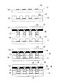
- FIG. 1A to FIG. 1F are cross-sectional views in order of steps showing a first specific example of the electronic component mounting method of the present invention.
- a wiring board 1 having electrode terminals 2 formed on the surface is prepared (FIG. 1 (a)).
- the material of the wiring board is, for example, FR4 (glass epoxy board).
- a resist pattern 3 is formed on the exposed surface of the wiring board 1 other than the electrode terminals 2 (FIG. 1B).
- bumps 4 made of solder are formed on the electrode terminals 2 (FIG. 1 (c)).
- an electronic component having a pillar formed on the surface for example, a semiconductor chip is positioned so that the surface on which the pillar is formed faces the solder bump 4 on the wiring substrate 1 (FIG. 1 (d)).
- the semiconductor chip has an electrode terminal 7 on a chip substrate 5 and is connected to the electrode terminal 7 to form a copper pillar 8.
- the surface of the copper pillar 8 is solder-plated and covered with a solder coating 9.
- the copper pillar 9 and the solder bump 4 are joined (FIG. 1 (e)).
- the underfill material is heated to be liquid and then injected into the space formed between the semiconductor chip and the wiring board. Further, the underfill material is cured by heating to the curing temperature of the resin (FIG. 1 (f)). Since the only metal in contact with the underfill material 10 is solder, no local battery is formed, and no filler separation occurs.
- the underfill material is prepared by mixing a resin, a curing agent, and a filler. Further, it may be prepared by mixing a diluent and a curing accelerator. Further, the mounting method of the present invention is not limited to the materials shown below, and an effect excellent in preventing filler separation can be obtained even when a material other than the materials shown below is used.
- an epoxy resin is preferably used as the resin constituting the underfill material.
- the epoxy resin is not particularly limited as long as it is an epoxy compound that has two or more epoxy groups in one molecule and is cured to form a resin.
- the epoxy resin is bisphenol A type epoxy resin, brominated bisphenol A type epoxy resin, bisphenol F type epoxy resin, biphenyl type epoxy resin, novolac type epoxy resin, alicyclic epoxy resin, naphthalene type epoxy resin, Examples include ether-based or polyether-based epoxy resins, oxirane ring-containing polybutadiene, silicone epoxy copolymer resins, and the like.
- a diluent When a diluent is used, either a non-reactive diluent or a reactive diluent can be used, but it is more preferable to use a reactive diluent.
- a reactive diluent is a compound having one or two or more epoxy groups in one molecule and having a relatively low viscosity at room temperature.
- epoxy group other polymerizable functional groups, For example, you may have alkenyl groups, such as vinyl and allyl, or unsaturated carboxylic acid residues, such as acryloyl and methacryloyl.
- Such reactive diluents include n-butyl glycidyl ether, 2-ethylhexyl glycidyl ether, phenyl glycidyl ether, cresyl glycidyl ether, ps-butylphenyl glycidyl ether, styrene oxide, ⁇ -pinene oxide, and the like.
- Monoepoxide compounds allyl glycidyl ether, glycidyl methacrylate, monoepoxide compounds having functional groups such as 1-vinyl-3,4-epoxycyclohexane, (poly) ethylene glycol diglycidyl ether, (poly) propylene glycol diglycidyl ether Diepoxide compounds such as butanediol glycidyl ether, neopentyl glycol glycidyl ether, trimethylolpropane triglycidyl ether, glycerin triglycidyl ether And triepoxide compounds such as [Curing agent] When an epoxy resin is used as the resin material for the underfill material, a phenol resin, an acid anhydride, or an amine compound can be used as the curing agent.
- a phenol resin, an acid anhydride, or an amine compound can be used as the curing agent.
- phenol resin examples include phenol novolac resin, cresol novolac resin, naphthol modified phenol resin, dicyclopentadiene modified phenol resin, p-xylene modified phenol resin, dicyclopentadiene modified phenol resin, p-xylene modified phenol resin and the like. However, it is not limited to these, What is necessary is just to be normally used for the resin composition for underfills.
- the OH equivalent in the phenol resin is preferably 0.3 to 1.5 equivalent, more preferably 0.5 to 1.2 equivalent, per equivalent of epoxy group in the epoxy resin.
- Examples of acid anhydrides include methyl tetrahydrophthalic anhydride, methyl hexahydrophthalic anhydride, alkylated tetrahydrophthalic anhydride, hexahedrophthalic anhydride, methyl hymic anhydride, dodecenyl succinic anhydride, methyl nadic anhydride Etc. are exemplified.
- the blending ratio of the epoxy resin and the acid anhydride is preferably such that the equivalent of the acid anhydride is 0.6 to 1.0 equivalent per equivalent of the epoxy group in the epoxy resin.
- amine compounds include, but are not limited to, aliphatic polyamines, aromatic amines, and modified polyamines such as polyaminoamides, polyaminoimides, polyamino esters, and polyaminoureas. Further, tertiary amine, imidazole, hydrazide, dicyandiamide, and melamine compounds can be used.
- the blending ratio of the epoxy resin and the amine compound is preferably such that the equivalent of the amine compound is 0.6 to 1.0 equivalent per equivalent of epoxy group in the epoxy resin.
- These curing agents may be used alone or in combination of two or more.
- a curing accelerator can be used for the underfill material as necessary.
- Examples of the curing accelerator include imidazole series, tertiary amine series, and phosphorus compound series. Examples include 2-methylimidazole, 2-undecylimidazole, 2-heptadecylimidazole, 2-ethyl-4-methylimidazole, 2-phenylimidazole, 2-phenyl-4-methylimidazole, etc. It is not limited to.
- the blending amount of the curing accelerator is preferably set to a ratio of 0.05 to 30% by weight of the entire resin composition. Further, these curing accelerators may be used alone or in combination of two or more. [Filler] Examples of the filler blended in the underfill material include fused silica, aluminum nitride, and fused alumina.
- the shape is preferably spherical, and the average particle size is preferably in the range of 0.2 ⁇ m to 20 ⁇ m, and is preferably set as appropriate according to the semiconductor design, sealing method, and the like. You may mix and use the filler of a different material and particle diameter. In addition to the filler, a silane coupling agent, a surfactant, an elastomer, and the like may be appropriately blended with the underfill material.
- the second specific example of the mounting method of the present invention is a modification of the first specific example, and differs from the first specific example in that solder bumps are formed not on the wiring board side but on the semiconductor chip side.
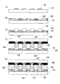
- 2A to 2E are cross-sectional views in order of steps showing a second specific example of the electronic component mounting method of the present invention.
- a wiring board 51 having electrode terminals 52 formed on the surface is prepared (FIG. 2A).
- a resist pattern 53 is formed on the exposed surface of the wiring board 51 other than the electrode terminals 52 (FIG. 2B).
- an electronic component having pillars and solder bumps formed on its surface for example, a semiconductor chip is positioned by placing the surface on which the pillars and solder bumps are formed facing the electrode terminals 52 on the wiring board 51 ( FIG. 2 (c)).
- the semiconductor chip has an electrode terminal 57 on a chip substrate 55, a copper pillar 58 is formed by being connected to the electrode terminal 57, and a solder bump 54 is formed by being connected to the copper pillar 58.
- the surface of the copper pillar 58 is solder-plated and covered with a solder coating 59.
- the solder bump 54 and the electrode terminal 52 are joined (FIG. 2D).
- the underfill material is heated to be liquid and then injected into the space formed between the semiconductor chip and the wiring board. Furthermore, the underfill material is cured by heating to the curing temperature of the resin (FIG. 2 (e)). Since the only metal in contact with the underfill material 60 is solder, a local battery is not formed, and filler separation does not occur.
- the second solution of the present invention is to prevent the filler from separating by forming a thick resist for preventing a short circuit of the solder to prevent contact between the solder and the underfill.
- 3A to 3E are cross-sectional views in order of steps showing a third specific example of the electronic component mounting method of the present invention.
- the wiring substrate 11 having the electrode terminals 12 formed on the surface is prepared (FIG. 3A).
- a resist pattern 13 is formed on the exposed surface of the wiring board 11 other than the electrode terminals 12 (FIG. 3B).
- an electronic component having pillars and solder bumps formed on its surface for example, a semiconductor chip is positioned by placing the surface on which the pillars and solder bumps are formed facing the electrode terminals 12 on the wiring board 11 ( FIG. 3 (c)).
- the semiconductor chip has an electrode terminal 15 on a chip substrate 14, a copper pillar 17 is formed by connecting to the electrode terminal 15, and a solder bump 18 is formed by connecting to the copper pillar 17.
- the solder bump 18 and the electrode terminal 12 are joined (FIG. 3 (d)).
- the thickness of the resist pattern is thicker than the thickness of the solder bump compressed in the process shown in FIG. To form.
- the underfill material is heated to be liquid and then injected into the space formed between the semiconductor chip and the wiring board. Further, the underfill material is cured by heating to the curing temperature of the resin (FIG. 3 (e)). Since the only metal in contact with the underfill material 19 is copper, a local battery is not formed, and filler separation does not occur. According to the second solving means of the present invention, there is no need for a step of performing solder plating on the surface of the copper pillar, so that there is an effect that the manufacturing cost can be reduced.
- filler separation is prevented by applying a voltage of 0.1 to several volts by setting the copper side to a negative voltage and the solder side to a positive voltage. it can.
- AC voltage application It turned out that filler isolation
- the applied voltage and frequency are appropriately set in consideration of the underfill material, metal material, curing conditions, and the like.
- Reduction of curing time It was found that filler separation can be prevented by shortening the curing time.
- the curing time is preferably 30 seconds to 1 hour. Specific methods for shortening the curing time include raising the curing temperature and adding a curing accelerator.
- the problem-solving means according to the present invention for preventing the filler separation listed above is the case where the pillar is not copper or gold, or the bump is not solder, and the curing agent contained in the underfill is amine-based. Even if it is not a curing agent, it goes without saying that an excellent effect can be obtained by adopting it as a method for preventing filler separation in any flip chip mounting in which a dissimilar metal comes into contact with the underfill material.
- the filler does not collect at a place where the filler, such as the electrode connection portion, is desired to be aggregated.
- the problem-solving means according to the present invention it is possible to uniformly disperse the filler in the resin, control the distribution of the filler, for example, increase the filler density at the place where the filler is to be aggregated, It is also possible to enhance the reinforcement of the bump.
- the separation of the filler in the underfill is controlled, and the filler is uniformly dispersed or aggregated in a necessary region to be cured. As a result, the connection reliability of flip chip mounting can be improved.
Landscapes
- Chemical & Material Sciences (AREA)
- Health & Medical Sciences (AREA)
- Chemical Kinetics & Catalysis (AREA)
- Medicinal Chemistry (AREA)
- Polymers & Plastics (AREA)
- Organic Chemistry (AREA)
- Wire Bonding (AREA)
- Encapsulation Of And Coatings For Semiconductor Or Solid State Devices (AREA)
- Structures Or Materials For Encapsulating Or Coating Semiconductor Devices Or Solid State Devices (AREA)
- Non-Metallic Protective Coatings For Printed Circuits (AREA)
Abstract
Description
特許文献1には、エポキシ樹脂と、多官能脂肪族エポキシと、塩基性硬化剤と、無機フィラーとからなるアンダーフィル材が開示されている。エポキシ樹脂用の硬化剤としては、一般的に、フェノール系、酸無水系、又は、アミン系の硬化剤が知られているが、近年、ガラス転移温度の制御性に優れていることからアミン系など塩基性の硬化剤を混合したアンダーフィル材が多く使用される。
シリコンチップの線膨張係数は4pm/℃であり、基板、例えば、ガラスエポキシ基板の線膨張率は20ppm/℃である。フィラーはこの線膨張率の差を吸収するために混合するもので、例えば、シリカ、アルミナ、窒化ホウ素、窒化アルミニウムからなる粉末が通常用いられる。
一方、近年、特に高密度のフリップチップ実装において、銅ピラーバンプが用いられるようになった。銅ピラーバンプは、従来のはんだバンプと比較して、バンプのピッチを小さくできる、鉛の使用量を低減できるので環境に与える影響が小さい、熱伝導性が高いので放熱特性に優れている、電気伝導度が高いので寄生抵抗を低減できるなどの利点がある。
しかし、図7に示すような実装方法で、銅ピラーを用いたフリップチップ実装を行うと、アンダーフィル中のフィラーが加熱硬化中に樹脂から分離する(樹脂中で凝集する)という現象が発生することがわかった。このため、アンダーフィル樹脂中にフィラーが存在しない領域が形成されることとなり、シリコンチップと基板の線膨張率の差を吸収できず、バンプにクラックが発生するなどの問題が発生した。
本発明(2)は、金属ピラーを備えた電子部品をはんだバンプを介して基板表面に配置した複数の電極端子に接続する実装方法において、少なくとも、前記はんだバンプより厚いレジストパターンを前記電極端子と隣り合う前記電極端子の間に形成する工程と、前記電子部品と前記基板の間にフィラーを含むアンダーフィル材を注入し、加熱硬化する工程とからなる電子部品の実装方法である。
本発明(3)は、金属ピラーを備えた電子部品をはんだバンプを介して基板表面に配置した複数の電極端子に接続する実装方法において、少なくとも、前記電子部品と前記基板の間にフィラーを含むアンダーフィル材を注入する工程と、前記アンダーフィル材の徐電を行った後に前記アンダーフィル材を加熱硬化する工程とからなる電子部品の実装方法である。
本発明(4)は、金属ピラーを備えた電子部品をはんだバンプを介して基板表面に配置した複数の電極端子に接続する実装方法において、少なくとも、前記電子部品と前記基板の間にフィラーを含むアンダーフィル材を注入する工程と、前記アンダーフィル材に直流電界を印加しながら、前記アンダーフィル材を加熱硬化する工程とからなる電子部品の実装方法である。
本発明(5)は、金属ピラーを備えた電子部品をはんだバンプを介して基板表面に配置した複数の電極端子に接続する実装方法において、少なくとも、前記電子部品と前記基板の間にフィラーを含むアンダーフィル材を注入する工程と、前記アンダーフィル材に交流電界を印加しながら、前記アンダーフィル材を加熱硬化する工程とからなる電子部品の実装方法である。
本発明(6)は、金属ピラーを備えた電子部品をはんだバンプを介して基板表面に配置した複数の電極端子に接続する実装方法において、少なくとも、前記電子部品と前記基板の間にフィラーを含むアンダーフィル材を注入する工程と、前記アンダーフィル材を加熱硬化する工程とからなり、前記加熱硬化の時間が30秒以上1時間以下であることを特徴とする電子部品の実装方法である。
本発明(7)は、前記金属ピラーが、銅又は金からなるピラーであることを特徴とする前記発明(1)乃至前記発明(6)の電子部品の実装方法である。
本発明(8)は、前記アンダーフィル材が、エポキシ系樹脂からなるアンダーフィル材であり、アミン系硬化剤とフィラーとを含むことを特徴とする前記発明(1)乃至前記発明(7)の電子部品の実装方法である。
本発明(9)は、金属ピラーを備えた電子部品をはんだバンプを介して基板表面に配置した複数の電極端子に接続した実装基板において、前記金属ピラーの表面がはんだで被膜されていることを特徴とする実装基板である。
本発明(10)は、金属ピラーを備えた電子部品をはんだバンプを介して基板表面に配置した複数の電極端子に接続した実装基板において、前記はんだバンプの表面がレジストで覆われていることを特徴とする実装基板である。
本発明(11)は、前記実装基板が、前記電子部品と前記基板の間にフィラーを含むアンダーフィル材を注入し、加熱硬化した実装基板であり、前記金属ピラーの表面が前記アンダーフィル材に接触しないように、はんだで被膜されていることを特徴とする前記発明(9)の実装基板である。
本発明(12)は、前記実装基板が、前記電子部品と前記基板の間にフィラーを含むアンダーフィル材を注入し、加熱硬化した実装基板であり、前記はんだバンプの表面が前記アンダーフィル材に接触しないように、レジストで覆われていることを特徴とする前記発明(10)の実装基板である。
本発明(13)は、前記金属ピラーが、銅又は金からなるピラーであることを特徴とする前記発明(9)又は前記発明(12)の実装基板である。
本発明(14)は、前記アンダーフィル材が、エポキシ系樹脂からなるアンダーフィル材であり、アミン系硬化剤とフィラーとを含むことを特徴とする前記発明(11)乃至前記発明(13)の実装基板である。
2、12、52、102 電極端子
3、13、53、103 レジストパターン
4、18、54、104 はんだ
5、14、55、106 チップ基板
6、16、56、108 パッシベーション
7、15、57、107 電極端子
8、17、58、105 銅ピラー
9、59 はんだめっき
10、19、60、109 アンダーフィル
31 配線基板
32 レジストパターン
33、43、48 ファラーが集積した領域
42、47 はんだめっき被膜
34、44、49 フィラーがほとんど存在しない領域
35 チップ基板
36 電極端子
37、40、46 はんだ
38、41、45 銅ピラー
39 クラック
(フィラーとアンダーフィル樹脂の分離)
本願発明者等は、銅ピラーバンプを用いた電子部品と実装基板の間にアンダーフィルを注入してから、加熱してアンダーフィルを硬化させた後に、アンダーフィルの断面を観察したところ、加熱前はアンダーフィル中に均一に分散していたフィラーが樹脂中で凝集して、銅ピラーの近傍にはフィラーが存在しなくなる現象を見出した。従来のはんだバンプ実装の場合でも、アンダーフィル中に分散した一部のフィラー粒子が加熱硬化中に重力によって沈降することはあったが、銅ピラーの場合は、高い再現性でほとんどすべてのフィラー粒子が銅ピラー近傍から分離することがわかった。先に述べたように、フィラーがアンダーフィル樹脂中に均一に分散していないと、電子部品と基板の線膨張率の差を適切に吸収できないという問題が発生する。
このフィラーの分離は、フェノール系や無水酸系の硬化剤を用いる場合は、あまり観察されなかった。また、はんだやレジストなどの耐熱性など、実装プロセスの制限から、アンダーフィルの加熱温度を170℃以上にすることができない場合に、フィラーの分離が高い頻度で発生することがわかった。アミン系硬化剤は、フェノール系や無水酸系の硬化剤と比較して硬化促進性が低く硬化時間が長い。例えば、フェノール系硬化剤を用いた場合に150℃30分の加熱を硬化に要していたのに対し、アミン系硬化剤を用いた場合は、150℃1時間から2時間の加熱を要する。すなわち、加熱時間が長い場合に、分離が発生することがわかった。
本願発明者等は、フィラーの分離の原因が、異種金属の接触による局所電池の形成ではないかと推定して、原因の調査実験を行った。図5(a)は、フィラーと樹脂の分離に対する帯電の影響を調査する実験方法を説明する図である。まず、表面にくし型電極を印刷した基板を用意し、アンダーフィル(UF)がくし型電極上にかかるように塗布した。次に、電極に直流電圧(20V)を印加してアンダーフィルを帯電し、その状態で、アンダーフィルを加熱して硬化させた。図5(b)は、電圧を印加した場合の試験片の断面図である。左側が負電圧印加電極、右側が正電圧印加電極である。正電圧印加電極の近傍にはフィラーが存在していないことがわかる。図5(c)は、電圧を印加しない場合の試験片の断面図である。隣接する二つの電極のどちらの近傍においても、フィラーの分布に顕著な差が生じていないことがわかる。この実験の結果、アンダーフィル中に分散した帯電したフィラーが局部電池により反発して分離している可能性が高いことが確認できた。
フィラーの分離が、異種金属の接触による局部電池であることを確認するため、さらに調査実験を行った。図6(a)は、フィラーと樹脂の分離に対する局部電池の影響を調査する実験方法を説明する図である。まず、基板上にはんだバンプ(Pb/Sn)を乗せ、その上にシリコンチップを乗せた試料を用意した。基板材料として、FR4(ガラスエポキシ基板)、銅、金の3種類の基板を用いた試料を用意した。次に、シリコンチップと基板の間にアンダーフィルを注入し、加熱して硬化させ、SEMにより断面観察を行った。図6(b)乃至(d)は、実験結果を示すSEM写真である。基板がFR4の場合は、フィラーの分離は観察されなかった。一方、基板が銅又は金の場合は、銅や金から離れ、はんだに近づくようにフィラーの分離が発生することがわかった。この結果から、異種金属の接触による局部電池によりフィラーの分離が発生していることが確認できた。また、銅ピラーバンプだけでなく、金からなるピラーを用いた場合や、金線を用いて接続する場合、さらに、銅、金だけでなく、異なる2種以上の金属をアンダーフィルに接触させた場合にも、フィラーの分離が発生すると予測できる。
本願発明者等は、フィラー分離の問題に関して得られた知見を基に、問題解決の手段を検討した。その結果、複数の解決手段を見出し、評価を行ったところそれらの手段が実際に問題の解決に有効であることが確認できた。
本発明の第一の解決手段は、銅ピラーの表面をはんだでめっきして、銅がアンダーフィルに接触しないようにする方法である。図1(a)乃至(f)は、本発明の電子部品の実装方法の第一の具体例を示す工程順断面図である。最初に、電極端子2が表面に形成された配線基板1を用意する(図1(a))。配線基板の材料は、例えば、FR4(ガラスエポキシ基板)である。次に、配線基板1の電極端子2以外の露出した表面にレジストパターン3を形成する(図1(b))。次に、電極端子2の上にはんだからなるバンプ4を形成する(図1(c))。次に、表面にピラーが形成された電子部品、例えば、半導体チップをピラーが形成された面を配線基板1上のはんだバンプ4と向かい合うように置いて位置合わせを行う(図1(d))。半導体チップは、チップ基板5上に電極端子7があり、電極端子7に接続して銅ピラー8が形成されている。銅ピラー8の表面ははんだめっきを行い、はんだ被膜9により覆われている。次に、銅ピラー9とはんだバンプ4を接合する(図1(e))。最後に、アンダーフィル材を加熱して液状にしてから、半導体チップと配線基板の間に形成された空間に注入する。さらに、アンダーフィル材を樹脂の硬化温度まで加熱して硬化する(図1(f))。アンダーフィル材10と接触する金属は、はんだだけであるので、局部電池は形成されず、フィラーの分離は発生しない。
本発明の実装方法を適用してフィラーの分離に有効なアンダーフィル材料は、例えば、以下の材料が挙げられる。アンダーフィル材は、樹脂、硬化剤、フィラーを混合して調製される。さらに、希釈剤、硬化促進剤を混合して調製する場合もある。また、本発明の実装方法は、以下に示す材料に限定されるものではなく、以下に示す材料以外の材料を用いた場合でもフィラー分離の防止に優れた効果が得られる。
[樹脂]
アンダーフィル材を構成する樹脂は、例えば、エポキシ樹脂を用いるのが好ましい。エポキシ樹脂は、1分子中に2個以上のエポキシ基を有し、硬化して樹脂状になるエポキシ化合物であれば、特に、限定されない。エポキシ樹脂は、具体的には、ビスフェノールA型エポキシ樹脂、臭素化ビスフェノールA型エポキシ樹脂、ビスフェノールF型エポキシ樹脂、ビフェニル型エポキシ樹脂、ノボラック型エポキシ樹脂、脂環式エポキシ樹脂、ナフタレン型エポキシ樹脂、エーテル系又はポリエーテル系エポキシ樹脂、オキシラン環含有ポリブタジエン、シリコーンエポキシコポリマー樹脂等が例示される。
[希釈剤]
希釈剤を用いる場合、非反応性希釈剤及び反応性希釈剤のいずれをも使用することができるが、反応性希釈剤を用いるのがより好ましい。反応性希釈剤は、1分子中に1個又は2個以上のエポキシ基を有する、常温で比較的低粘度の化合物であり、目的に応じて、エポキシ基以外に、他の重合性官能基、例えば、ビニル、アリル等のアルケニル基、又は、アクリロイル、メタクリロイル等の不飽和カルボン酸残基を有していてもよい。このような反応性希釈剤としては、n―ブチルグリシジルエーテル、2―エチルヘキシルグリシジルエーテル、フェニルグリシジルエーテル、クレジルグリシジルエーテル、p-s―ブチルフェニルグリシジルエーテル、スチレンオキシド、α―ピネンオキシドのようなモノエポキシド化合物、アリルグリシジルエーテル、メタクリル酸グリシジル、1―ビニル―3, 4―エポキシシクロヘキサンのような官能基を有するモノエポキシド化合物、(ポリ)エチレングリコールジグリシジルエーテル、(ポリ)プロピレングリコールジグルシジルエーテル、ブタンジオールグリシジルエーテル、ネオペンチルグリコールグリシジルエーテルのようなジエポキシド化合物、トリメチロールプロパントリグリシジルエーテル、グリセリントリグリシジルエーテルのようなトリエポキシド化合物等が例示される。
[硬化剤]
アンダーフィル材の樹脂材料として、エポキシ樹脂を用いる場合は、硬化剤は、フェノール樹脂、酸無水物、又は、アミン系化合物を用いることができる。
フェノール樹脂としては、フェノールノボラック樹脂、クレゾールノボラック樹脂、ナフトール変性フェノール樹脂、ジシクロペンタジエン変性フェノール樹脂、p―キシレン変性フェノール樹脂、ジシクロペンタジエン変性フェノール樹脂、p―キシレン変性フェノール樹脂等が例示されるが、これらに限定されるものではなく、アンダーフィル用樹脂組成物に通常用いられるものであればよい。
エポキシ樹脂中のエポキシ基1当量あたり、フェノール樹脂中のOH当量が、0.3~1.5当量となることが好ましく、0.5~1.2当量となることがより好ましい。
酸無水物としては、メチルテトラヒドロフタル酸無水物、メチルヘキサヒドロフタル酸無水物、アルキル化テトラヒドロフタル酸無水物、ヘキサヘドロフタル酸無水物、無水メチルハイミック酸、無水ドデセニルコハク酸、無水メチルナジック酸等が例示される。
エポキシ樹脂と酸無水化物の配合割合は、エポキシ樹脂中のエポキシ基1当量あたり、酸無水化物の当量が0.6~1.0当量となることが好ましい。
アミン系化合物としては、脂肪族ポリアミン、芳香族アミン、及び、ポリアミノアミド、ポリアミノイミド、ポリアミノエステル、ポリアミノ尿素等の変性ポリアミンが例示されるが、これらに限定されるものではない。また、第三級アミン系、イミダゾール系、ヒドラジド系、ジシアンジアミド系、メラミン系の化合物を用いることができる。
エポキシ樹脂とアミン系化合物の配合割合は、エポキシ樹脂中のエポキシ基1当量あたり、アミン系化合物の当量が0.6~1.0当量となることが好ましい。
また、これらの硬化剤は、単独で用いてもよく、2種以上併用してもよい。
[硬化促進剤]
アンダーフィル材には、必要に応じて、硬化促進剤を用いることができる。硬化促進剤としては、イミダゾール系、第三級アミン系、リン化合物系等が挙げられ。例えば、2―メチルイミダゾール、2―ウンデシルイミダゾール、2―ヘプタデシルイミダゾール、2―エチル―4―メチルイミダゾール、2―フェニルイミダゾール、2―フェニル―4―メチルイミダゾール等が例示されるが、特にこれらに限定されるものではない。硬化促進剤の配合量は、樹脂組成物全体の0.05~30重量%の割合に設定することが好ましい。また、これらの硬化促進剤は、単独で用いてもよく、2種以上併用してもよい。
[フィラー]
アンダーフィル材に配合するフィラーとしては、溶融シリカ、窒化アルミ、溶融アルミナ等が例示される。形状としては、球状が好ましく、平均粒子径は、0.2μmから20μmの範囲とするのが好ましく、半導体のデザインや封止方法等に応じて適宜設定するのが好ましい。異なる材料、粒子径のフィラーを混合して使用してもよい。
アンダーフィル材には、フィラー以外にも、シランカップリング剤、界面活性剤、エラストマー等を適宜配合してもよい。
本発明の実装方法の第二の具体例、第一の具体例の変形例であり、はんだバンプが配線基板側ではなく、半導体チップ側に形成される点で、第一の具体例と異なる。
図2(a)乃至(e)は、本発明の電子部品の実装方法の第二の具体例を示す工程順断面図である。最初に、電極端子52が表面に形成された配線基板51を用意する(図2(a))。次に、配線基板51の電極端子52以外の露出した表面にレジストパターン53を形成する(図2(b))。次に、表面にピラー及びはんだバンプが形成された電子部品、例えば、半導体チップをピラー及びはんだバンプが形成された面を配線基板51上の電極端子52と向かい合うように置いて位置合わせを行う(図2(c))。半導体チップは、チップ基板55上に電極端子57があり、電極端子57に接続して銅ピラー58が形成され、銅ピラー58に接続してはんだバンプ54が形成されている。銅ピラー58の表面ははんだめっきを行い、はんだ被膜59により覆われている。次に、はんだバンプ54と電極端子52を接合する(図2(d))。最後に、アンダーフィル材を加熱して液状にしてから、半導体チップと配線基板の間に形成された空間に注入する。さらに、アンダーフィル材を樹脂の硬化温度まで加熱して硬化する(図2(e))。アンダーフィル材60と接触する金属は、はんだだけであるので、局部電池は形成されず、フィラーの分離は発生しない。
本発明の第二の解決手段は、はんだの短絡を防止するためのレジストを厚く形成することにより、はんだとアンダーフィルの接触を防止ことにより、フィラーの分離を防止するものである。図3(a)乃至(e)は、本発明の電子部品の実装方法の第三の具体例を示す工程順断面図である。最初に、電極端子12が表面に形成された配線基板11を用意する(図3(a))。次に、配線基板11の電極端子12以外の露出した表面にレジストパターン13を形成する(図3(b))。次に、表面にピラー及びはんだバンプが形成された電子部品、例えば、半導体チップをピラー及びはんだバンプが形成された面を配線基板11上の電極端子12と向かい合うように置いて位置合わせを行う(図3(c))。半導体チップは、チップ基板14上に電極端子15あり、電極端子15に接続して銅ピラー17が形成され、銅ピラー17に接続してはんだバンプ18が形成されている。次に、はんだバンプ18と電極端子12を接合する(図3(d))。図3(b)に示すレジストパターンの形成工程において、レジストパターンの厚さは、図3(d)に示す工程において圧縮されたはんだバンプの厚さより厚くなり、はんだバンプを完全に覆う程度の厚さに形成する。最後に、アンダーフィル材を加熱して液状にしてから、半導体チップと配線基板の間に形成された空間に注入する。さらに、アンダーフィル材を樹脂の硬化温度まで加熱して硬化する(図3(e))。アンダーフィル材19と接触する金属は、銅だけであるので、局部電池は形成されず、フィラーの分離は発生しない。
本発明の第二の解決手段によれば、銅ピラーの表面にはんだめっきを行う工程が不要であるため、製造コストを低減できる効果がある。
本願発明者等は、見出したフィラー分離の原理に基づいて、以上挙げた具体例以外にも、さまざまな問題解決手段を考案し、効果の確認実験を行い、いずれの方法も顕著な効果が得られることを確認した。また、実装方法の改善以外に、アンダーフィル材料の改善を行っても、フィラー分離の防止に効果があることがわかった。以下に、上記した以外の本発明の実装方法及びアンダーフィル材の具体例について述べる。
(1)除電
アンダーフィル材を調製する段階、又は、アンダーフィル材を電子部品と配線基板の間に注入してから樹脂を硬化させるまでの間に、アンダーフィル材に対し徐電を行い、フィラーに発生した静電気を除去することで、フィラー分離の防止が可能であることがわかった。徐電の具体的手段としては、例えば、コロナ放電、紫外線照射が例示される。
(2)直流電圧印加
異種金属の接触により発生する局部電池の電圧を打ち消すように電極端子間に直流電圧を印加した状態でアンダーフィルの硬化を行うことで、フィラー分離の防止が可能であることがわかった。例えば、銅ピラーとはんだバンプがアンダーフィル材に接触している場合は、銅側を負電圧としはんだ側を正電圧とし、0.1~数ボルトの電圧を印加することにより、フィラー分離が防止できる。
(3)交流電圧印加
電極端子に、交流電圧を印加した状態でアンダーフィルの硬化を行うことで、フィラー分離の防止が可能であることがわかった。印加する電圧、周波数は、アンダーフィル材料、金属材料、硬化条件等を考慮して適宜設定する。
(4)硬化時間の短縮
硬化時間を短縮することで、フィラー分離の防止が可能であることがわかった。硬化時間は、30秒以上1時間以下とするのが好ましい。硬化時間を短縮する具体的な方法としては、硬化温度を上げる、硬化促進剤を入れるなどが例示される。
(5)フィラーが動きにくいものを入れる
アンダーフィル材に、フィラーが電界の印加により移動しにくい添加剤を入れることで、フィラー分離の防止が可能であることがわかった。
上記列挙したフィラー分離を防止する本発明に係る課題解決手段は、ピラーが銅や金ではない場合でも、或いは、バンプがはんだではない場合でも、また、アンダーフィルに含まれる硬化剤がアミン系の硬化剤ではない場合でも、異種金属がアンダーフィル材に接触するあらゆるフリップチップ実装において、フィラー分離を防止する方法として採用することにより優れた効果が得られることは言うまでもない。
また、フィラーの分離自体が問題となるというより、従来は、フィラーの分離を制御できなかったことが問題であった。そのため、電極の接続部などのフィラーが凝集して欲しい場所にフィラーが集まらず、そのため接続不良が発生していた。本発明に係る課題解決手段を用いることにより、フィラーを樹脂中で均一に分散されることも可能であるし、フィラーの分布を制御し、例えば、フィラーを凝集させたい場所のフィラー密度を高め、バンプの補強性を高めることも可能である。
Claims (14)
- 金属ピラーを備えた電子部品をはんだバンプを介して基板表面に配置した複数の電極端子に接続する実装方法において、少なくとも、前記金属ピラーの表面をはんだで被膜する工程と、前記電子部品と前記基板の間にフィラーを含むアンダーフィル材を注入し、加熱硬化する工程とからなる電子部品の実装方法。
- 金属ピラーを備えた電子部品をはんだバンプを介して基板表面に配置した複数の電極端子に接続する実装方法において、少なくとも、前記はんだバンプより厚いレジストパターンを前記電極端子と隣り合う前記電極端子の間に形成する工程と、前記電子部品と前記基板の間にフィラーを含むアンダーフィル材を注入し、加熱硬化する工程とからなる電子部品の実装方法。
- 金属ピラーを備えた電子部品をはんだバンプを介して基板表面に配置した複数の電極端子に接続する実装方法において、少なくとも、前記電子部品と前記基板の間にフィラーを含むアンダーフィル材を注入する工程と、前記アンダーフィル材の徐電を行った後に前記アンダーフィル材を加熱硬化する工程とからなる電子部品の実装方法。
- 金属ピラーを備えた電子部品をはんだバンプを介して基板表面に配置した複数の電極端子に接続する実装方法において、少なくとも、前記電子部品と前記基板の間にフィラーを含むアンダーフィル材を注入する工程と、前記アンダーフィル材に直流電界を印加しながら、前記アンダーフィル材を加熱硬化する工程とからなる電子部品の実装方法。
- 金属ピラーを備えた電子部品をはんだバンプを介して基板表面に配置した複数の電極端子に接続する実装方法において、少なくとも、前記電子部品と前記基板の間にフィラーを含むアンダーフィル材を注入する工程と、前記アンダーフィル材に交流電界を印加しながら、前記アンダーフィル材を加熱硬化する工程とからなる電子部品の実装方法。
- 金属ピラーを備えた電子部品をはんだバンプを介して基板表面に配置した複数の電極端子に接続する実装方法において、少なくとも、前記電子部品と前記基板の間にフィラーを含むアンダーフィル材を注入する工程と、前記アンダーフィル材を加熱硬化する工程とからなり、前記加熱硬化の時間が30秒以上1時間以下であることを特徴とする電子部品の実装方法。
- 前記金属ピラーが、銅又は金からなるピラーであることを特徴とする請求項1乃至6記載のいずれか1項の電子部品の実装方法。
- 前記アンダーフィル材が、エポキシ系樹脂からなるアンダーフィル材であり、アミン系硬化剤とフィラーとを含むことを特徴とする請求項1乃至7のいずれか1項記載の電子部品の実装方法。
- 金属ピラーを備えた電子部品をはんだバンプを介して基板表面に配置した複数の電極端子に接続した実装基板において、前記金属ピラーの表面がはんだで被膜されていることを特徴とする実装基板。
- 金属ピラーを備えた電子部品をはんだバンプを介して基板表面に配置した複数の電極端子に接続した実装基板において、前記はんだバンプの表面がレジストで覆われていることを特徴とする実装基板。
- 前記実装基板が、前記電子部品と前記基板の間にフィラーを含むアンダーフィル材を注入し、加熱硬化した実装基板であり、前記金属ピラーの表面が前記アンダーフィル材に接触しないように、はんだで被膜されていることを特徴とする請求項9記載の実装基板。
- 前記実装基板が、前記電子部品と前記基板の間にフィラーを含むアンダーフィル材を注入し、加熱硬化した実装基板であり、前記はんだバンプの表面が前記アンダーフィル材に接触しないように、レジストで覆われていることを特徴とする請求項10記載の実装基板。
- 前記金属ピラーが、銅又は金からなるピラーであることを特徴とする請求項9又は12のいずれか1項記載の実装基板。
- 前記アンダーフィル材が、エポキシ系樹脂からなるアンダーフィル材であり、アミン系硬化剤とフィラーとを含むことを特徴とする請求項11乃至13のいずれか1項記載の実装基板。
Priority Applications (3)
| Application Number | Priority Date | Filing Date | Title |
|---|---|---|---|
| JP2011503764A JP5707316B2 (ja) | 2009-03-12 | 2010-02-25 | 電子部品の実装方法 |
| US13/138,582 US8586467B2 (en) | 2009-03-12 | 2010-02-25 | Method of mounting electronic component and mounting substrate |
| CN201080011333.4A CN102349141B (zh) | 2009-03-12 | 2010-02-25 | 电子元件的安装方法及安装基板 |
Applications Claiming Priority (2)
| Application Number | Priority Date | Filing Date | Title |
|---|---|---|---|
| JP2009-059618 | 2009-03-12 | ||
| JP2009059618 | 2009-03-12 |
Publications (1)
| Publication Number | Publication Date |
|---|---|
| WO2010103934A1 true WO2010103934A1 (ja) | 2010-09-16 |
Family
ID=42728224
Family Applications (1)
| Application Number | Title | Priority Date | Filing Date |
|---|---|---|---|
| PCT/JP2010/052991 Ceased WO2010103934A1 (ja) | 2009-03-12 | 2010-02-25 | アンダーフィル材、及び、電子部品の実装方法 |
Country Status (7)
| Country | Link |
|---|---|
| US (1) | US8586467B2 (ja) |
| JP (1) | JP5707316B2 (ja) |
| KR (1) | KR101609015B1 (ja) |
| CN (1) | CN102349141B (ja) |
| MY (1) | MY152729A (ja) |
| TW (1) | TWI509751B (ja) |
| WO (1) | WO2010103934A1 (ja) |
Cited By (7)
| Publication number | Priority date | Publication date | Assignee | Title |
|---|---|---|---|---|
| WO2012111439A1 (ja) * | 2011-02-15 | 2012-08-23 | 東レエンジニアリング株式会社 | 実装方法および実装装置 |
| JP2014521935A (ja) * | 2011-07-22 | 2014-08-28 | アレグロ・マイクロシステムズ・エルエルシー | 磁界変換器を有する電流センサの強化絶縁 |
| JP2016519420A (ja) * | 2013-03-13 | 2016-06-30 | 日本テキサス・インスツルメンツ株式会社 | 銅ピラー取り付け基板 |
| KR20160091887A (ko) | 2013-11-29 | 2016-08-03 | 나믹스 가부시끼가이샤 | 에폭시 수지 조성물, 반도체 봉지제 및 반도체 장치 |
| US10345343B2 (en) | 2013-03-15 | 2019-07-09 | Allegro Microsystems, Llc | Current sensor isolation |
| CN115458485A (zh) * | 2021-06-09 | 2022-12-09 | 矽品精密工业股份有限公司 | 电子封装件及其制法 |
| US11768230B1 (en) | 2022-03-30 | 2023-09-26 | Allegro Microsystems, Llc | Current sensor integrated circuit with a dual gauge lead frame |
Families Citing this family (13)
| Publication number | Priority date | Publication date | Assignee | Title |
|---|---|---|---|---|
| KR101849117B1 (ko) * | 2011-10-19 | 2018-04-18 | 에스케이하이닉스 주식회사 | 연결 범프를 포함하는 전자 소자의 패키지, 전자 시스템 및 제조 방법 |
| US8970034B2 (en) * | 2012-05-09 | 2015-03-03 | Micron Technology, Inc. | Semiconductor assemblies and structures |
| JP5594324B2 (ja) * | 2012-06-22 | 2014-09-24 | 株式会社村田製作所 | 電子部品モジュールの製造方法 |
| US8932909B2 (en) * | 2012-11-14 | 2015-01-13 | International Business Machines Corporation | Thermocompression for semiconductor chip assembly |
| US20150001736A1 (en) * | 2013-06-29 | 2015-01-01 | Hualiang Shi | Die connections using different underfill types for different regions |
| CN104347547B (zh) * | 2013-07-26 | 2018-03-02 | 日月光半导体制造股份有限公司 | 半导体封装件及其的制造方法 |
| CN104517928B (zh) * | 2013-09-30 | 2018-08-24 | 联华电子股份有限公司 | 具微细导电柱的半导体元件及其制造方法 |
| US10153180B2 (en) * | 2013-10-02 | 2018-12-11 | Taiwan Semiconductor Manufacturing Company, Ltd. | Semiconductor bonding structures and methods |
| US20160322342A1 (en) * | 2014-01-15 | 2016-11-03 | Panasonic Intellectual Property Management Co. Lt | Semiconductor device |
| US9595482B2 (en) * | 2015-03-16 | 2017-03-14 | Taiwan Semiconductor Manufacturing Company, Ltd. | Structure for die probing |
| CN111063667B (zh) * | 2019-11-12 | 2021-07-13 | 通富微电子股份有限公司 | 一种集成电路封装体及其制备方法 |
| US11644485B2 (en) | 2021-10-07 | 2023-05-09 | Allegro Microsystems, Llc | Current sensor integrated circuits |
| US20230238345A1 (en) * | 2022-01-27 | 2023-07-27 | nD-HI Technologies Lab, Inc. | High-yielding and ultrafine pitch packages for large-scale ic or advanced ic |
Citations (5)
| Publication number | Priority date | Publication date | Assignee | Title |
|---|---|---|---|---|
| JPH11135671A (ja) * | 1997-10-29 | 1999-05-21 | Toshiba Corp | 導電性バンプの形成方法、半導体装置および実装回路装置 |
| JP2000100862A (ja) * | 1998-09-25 | 2000-04-07 | Seiko Instruments Inc | ベアチップ実装方法 |
| JP2002203874A (ja) * | 2000-12-28 | 2002-07-19 | Toray Eng Co Ltd | チップの実装方法 |
| JP2002334906A (ja) * | 2001-05-09 | 2002-11-22 | Matsushita Electric Ind Co Ltd | フリップチップの実装方法 |
| JP2006165303A (ja) * | 2004-12-08 | 2006-06-22 | Shinko Electric Ind Co Ltd | 半導体チップのフリップチップ接続方法およびフリップチップ接続構造およびそのフリップチップ接続構造を備えた半導体装置 |
Family Cites Families (9)
| Publication number | Priority date | Publication date | Assignee | Title |
|---|---|---|---|---|
| JPS6154636A (ja) * | 1984-08-24 | 1986-03-18 | Matsushita Electric Works Ltd | 半導体樹脂封止用金型 |
| US5121190A (en) * | 1990-03-14 | 1992-06-09 | International Business Machines Corp. | Solder interconnection structure on organic substrates |
| JP2869907B2 (ja) * | 1991-11-28 | 1999-03-10 | カシオ計算機株式会社 | 半導体装置の接続構造 |
| JP3378334B2 (ja) * | 1994-01-26 | 2003-02-17 | 株式会社東芝 | 半導体装置実装構造体 |
| JP3017485B2 (ja) * | 1998-01-23 | 2000-03-06 | アピックヤマダ株式会社 | 半導体装置の樹脂封止方法及び樹脂封止装置 |
| JP3664140B2 (ja) * | 2001-03-26 | 2005-06-22 | 株式会社デンソー | 電子部品の実装方法 |
| TWI245402B (en) * | 2002-01-07 | 2005-12-11 | Megic Corp | Rod soldering structure and manufacturing process thereof |
| JP4596875B2 (ja) * | 2004-10-06 | 2010-12-15 | 関西電力株式会社 | 樹脂で被覆した高耐電圧半導体装置及びその製造方法 |
| JP2007056070A (ja) | 2005-08-22 | 2007-03-08 | Fujitsu Ltd | フリップチップ型半導体装置用アンダーフィル材、並びにそれを用いたフリップチップ型半導体装置及びその製造方法 |
-
2010
- 2010-02-25 MY MYPI2011004176 patent/MY152729A/en unknown
- 2010-02-25 US US13/138,582 patent/US8586467B2/en active Active
- 2010-02-25 KR KR1020117020697A patent/KR101609015B1/ko active Active
- 2010-02-25 CN CN201080011333.4A patent/CN102349141B/zh active Active
- 2010-02-25 JP JP2011503764A patent/JP5707316B2/ja active Active
- 2010-02-25 WO PCT/JP2010/052991 patent/WO2010103934A1/ja not_active Ceased
- 2010-03-01 TW TW099105782A patent/TWI509751B/zh active
Patent Citations (5)
| Publication number | Priority date | Publication date | Assignee | Title |
|---|---|---|---|---|
| JPH11135671A (ja) * | 1997-10-29 | 1999-05-21 | Toshiba Corp | 導電性バンプの形成方法、半導体装置および実装回路装置 |
| JP2000100862A (ja) * | 1998-09-25 | 2000-04-07 | Seiko Instruments Inc | ベアチップ実装方法 |
| JP2002203874A (ja) * | 2000-12-28 | 2002-07-19 | Toray Eng Co Ltd | チップの実装方法 |
| JP2002334906A (ja) * | 2001-05-09 | 2002-11-22 | Matsushita Electric Ind Co Ltd | フリップチップの実装方法 |
| JP2006165303A (ja) * | 2004-12-08 | 2006-06-22 | Shinko Electric Ind Co Ltd | 半導体チップのフリップチップ接続方法およびフリップチップ接続構造およびそのフリップチップ接続構造を備えた半導体装置 |
Cited By (11)
| Publication number | Priority date | Publication date | Assignee | Title |
|---|---|---|---|---|
| WO2012111439A1 (ja) * | 2011-02-15 | 2012-08-23 | 東レエンジニアリング株式会社 | 実装方法および実装装置 |
| JP2012169495A (ja) * | 2011-02-15 | 2012-09-06 | Toray Eng Co Ltd | 実装方法および実装装置 |
| JP2014521935A (ja) * | 2011-07-22 | 2014-08-28 | アレグロ・マイクロシステムズ・エルエルシー | 磁界変換器を有する電流センサの強化絶縁 |
| JP2017049264A (ja) * | 2011-07-22 | 2017-03-09 | アレグロ・マイクロシステムズ・エルエルシー | 磁界変換器を有する電流センサの強化絶縁 |
| JP2016519420A (ja) * | 2013-03-13 | 2016-06-30 | 日本テキサス・インスツルメンツ株式会社 | 銅ピラー取り付け基板 |
| US10345343B2 (en) | 2013-03-15 | 2019-07-09 | Allegro Microsystems, Llc | Current sensor isolation |
| US10753963B2 (en) | 2013-03-15 | 2020-08-25 | Allegro Microsystems, Llc | Current sensor isolation |
| KR20160091887A (ko) | 2013-11-29 | 2016-08-03 | 나믹스 가부시끼가이샤 | 에폭시 수지 조성물, 반도체 봉지제 및 반도체 장치 |
| US10196513B2 (en) | 2013-11-29 | 2019-02-05 | Namics Corporation | Epoxy resin composition, semiconductor sealing agent, and semiconductor device |
| CN115458485A (zh) * | 2021-06-09 | 2022-12-09 | 矽品精密工业股份有限公司 | 电子封装件及其制法 |
| US11768230B1 (en) | 2022-03-30 | 2023-09-26 | Allegro Microsystems, Llc | Current sensor integrated circuit with a dual gauge lead frame |
Also Published As
| Publication number | Publication date |
|---|---|
| JPWO2010103934A1 (ja) | 2012-09-13 |
| TWI509751B (zh) | 2015-11-21 |
| CN102349141A (zh) | 2012-02-08 |
| MY152729A (en) | 2014-11-28 |
| US8586467B2 (en) | 2013-11-19 |
| JP5707316B2 (ja) | 2015-04-30 |
| KR101609015B1 (ko) | 2016-04-20 |
| US20110316149A1 (en) | 2011-12-29 |
| KR20120024534A (ko) | 2012-03-14 |
| CN102349141B (zh) | 2015-07-01 |
| TW201041094A (en) | 2010-11-16 |
Similar Documents
| Publication | Publication Date | Title |
|---|---|---|
| JP5707316B2 (ja) | 電子部品の実装方法 | |
| KR20100129694A (ko) | 다층 반도체 장치용 언더필재의 댐재 조성물 및 상기 댐재 조성물을 이용한 다층 반도체 장치의 제조 방법 | |
| CN106914710B (zh) | 树脂助焊剂焊膏和安装结构体 | |
| KR102582323B1 (ko) | 언더필용 수지 조성물, 전자 부품 장치 및 전자 부품 장치의 제조 방법 | |
| CN105658727A (zh) | 环氧树脂组合物、半导体密封剂及半导体装置 | |
| JP2019026715A (ja) | 一括封止用エポキシ樹脂組成物、電子装置およびその製造方法 | |
| JP3716237B2 (ja) | 封止剤樹脂組成物 | |
| JP2016135888A (ja) | 液状エポキシ樹脂組成物及び電子部品装置 | |
| JP5506170B2 (ja) | 実装構造体および電子機器 | |
| JP5862176B2 (ja) | 液状エポキシ樹脂組成物の選択方法及び製造方法、並びに電子部品装置の製造方法 | |
| JP3818267B2 (ja) | アンダーフィル用樹脂組成物及び半導体装置 | |
| JP2009057575A (ja) | 液状エポキシ樹脂組成物及び電子部品装置 | |
| JP6388228B2 (ja) | 半導体封止用液状エポキシ樹脂組成物とそれを用いた半導体装置 | |
| JP2000269387A (ja) | 半導体封止用樹脂及びこれを用いた半導体装置 | |
| JP7149099B2 (ja) | 半導体装置の製造方法 | |
| JP4700438B2 (ja) | 半導体装置の製造方法 | |
| JP5909318B2 (ja) | 電子部品実装体、および電子部品の実装方法 | |
| JP5929977B2 (ja) | 液状エポキシ樹脂組成物及び電子部品装置 | |
| JP2013100526A (ja) | 液状エポキシ樹脂組成物及び電子部品装置 | |
| KR20240027774A (ko) | 도전성 수지 조성물, 고열전도성 재료 및 반도체 장치 | |
| WO2005080502A1 (ja) | アンダーフィル用液状エポキシ樹脂組成物および同組成物を用いて封止した半導体装置 | |
| JP6332488B2 (ja) | 液状エポキシ樹脂組成物の選択方法及び製造方法、並びに電子部品装置及びその製造方法 | |
| JP2015232146A (ja) | 液状エポキシ樹脂組成物の選択方法及び製造方法、並びに電子部品装置及びその製造方法 | |
| KR20170089850A (ko) | 구리 범프용 액상 봉지재 및 그것에 사용하는 수지 조성물 | |
| JP2016040393A (ja) | 液状エポキシ樹脂組成物及び電子部品装置 |
Legal Events
| Date | Code | Title | Description |
|---|---|---|---|
| WWE | Wipo information: entry into national phase |
Ref document number: 201080011333.4 Country of ref document: CN |
|
| 121 | Ep: the epo has been informed by wipo that ep was designated in this application |
Ref document number: 10750688 Country of ref document: EP Kind code of ref document: A1 |
|
| WWE | Wipo information: entry into national phase |
Ref document number: 2011503764 Country of ref document: JP |
|
| ENP | Entry into the national phase |
Ref document number: 20117020697 Country of ref document: KR Kind code of ref document: A |
|
| WWE | Wipo information: entry into national phase |
Ref document number: 13138582 Country of ref document: US |
|
| WWE | Wipo information: entry into national phase |
Ref document number: 12011501798 Country of ref document: PH |
|
| NENP | Non-entry into the national phase |
Ref country code: DE |
|
| 122 | Ep: pct application non-entry in european phase |
Ref document number: 10750688 Country of ref document: EP Kind code of ref document: A1 |