WO2010087526A1 - 樹脂組成物 - Google Patents
樹脂組成物 Download PDFInfo
- Publication number
- WO2010087526A1 WO2010087526A1 PCT/JP2010/051664 JP2010051664W WO2010087526A1 WO 2010087526 A1 WO2010087526 A1 WO 2010087526A1 JP 2010051664 W JP2010051664 W JP 2010051664W WO 2010087526 A1 WO2010087526 A1 WO 2010087526A1
- Authority
- WO
- WIPO (PCT)
- Prior art keywords
- resin composition
- resin
- mass
- component
- manufactured
- Prior art date
- Legal status (The legal status is an assumption and is not a legal conclusion. Google has not performed a legal analysis and makes no representation as to the accuracy of the status listed.)
- Ceased
Links
Classifications
-
- C—CHEMISTRY; METALLURGY
- C08—ORGANIC MACROMOLECULAR COMPOUNDS; THEIR PREPARATION OR CHEMICAL WORKING-UP; COMPOSITIONS BASED THEREON
- C08G—MACROMOLECULAR COMPOUNDS OBTAINED OTHERWISE THAN BY REACTIONS ONLY INVOLVING UNSATURATED CARBON-TO-CARBON BONDS
- C08G59/00—Polycondensates containing more than one epoxy group per molecule; Macromolecules obtained by polymerising compounds containing more than one epoxy group per molecule using curing agents or catalysts which react with the epoxy groups
- C08G59/18—Macromolecules obtained by polymerising compounds containing more than one epoxy group per molecule using curing agents or catalysts which react with the epoxy groups ; e.g. general methods of curing
- C08G59/40—Macromolecules obtained by polymerising compounds containing more than one epoxy group per molecule using curing agents or catalysts which react with the epoxy groups ; e.g. general methods of curing characterised by the curing agents used
- C08G59/62—Alcohols or phenols
-
- C—CHEMISTRY; METALLURGY
- C08—ORGANIC MACROMOLECULAR COMPOUNDS; THEIR PREPARATION OR CHEMICAL WORKING-UP; COMPOSITIONS BASED THEREON
- C08G—MACROMOLECULAR COMPOUNDS OBTAINED OTHERWISE THAN BY REACTIONS ONLY INVOLVING UNSATURATED CARBON-TO-CARBON BONDS
- C08G59/00—Polycondensates containing more than one epoxy group per molecule; Macromolecules obtained by polymerising compounds containing more than one epoxy group per molecule using curing agents or catalysts which react with the epoxy groups
- C08G59/18—Macromolecules obtained by polymerising compounds containing more than one epoxy group per molecule using curing agents or catalysts which react with the epoxy groups ; e.g. general methods of curing
- C08G59/68—Macromolecules obtained by polymerising compounds containing more than one epoxy group per molecule using curing agents or catalysts which react with the epoxy groups ; e.g. general methods of curing characterised by the catalysts used
- C08G59/688—Macromolecules obtained by polymerising compounds containing more than one epoxy group per molecule using curing agents or catalysts which react with the epoxy groups ; e.g. general methods of curing characterised by the catalysts used containing phosphorus
-
- C—CHEMISTRY; METALLURGY
- C08—ORGANIC MACROMOLECULAR COMPOUNDS; THEIR PREPARATION OR CHEMICAL WORKING-UP; COMPOSITIONS BASED THEREON
- C08G—MACROMOLECULAR COMPOUNDS OBTAINED OTHERWISE THAN BY REACTIONS ONLY INVOLVING UNSATURATED CARBON-TO-CARBON BONDS
- C08G59/00—Polycondensates containing more than one epoxy group per molecule; Macromolecules obtained by polymerising compounds containing more than one epoxy group per molecule using curing agents or catalysts which react with the epoxy groups
- C08G59/18—Macromolecules obtained by polymerising compounds containing more than one epoxy group per molecule using curing agents or catalysts which react with the epoxy groups ; e.g. general methods of curing
- C08G59/40—Macromolecules obtained by polymerising compounds containing more than one epoxy group per molecule using curing agents or catalysts which react with the epoxy groups ; e.g. general methods of curing characterised by the curing agents used
- C08G59/50—Amines
- C08G59/56—Amines together with other curing agents
- C08G59/58—Amines together with other curing agents with polycarboxylic acids or with anhydrides, halides, or low-molecular-weight esters thereof
-
- C—CHEMISTRY; METALLURGY
- C08—ORGANIC MACROMOLECULAR COMPOUNDS; THEIR PREPARATION OR CHEMICAL WORKING-UP; COMPOSITIONS BASED THEREON
- C08J—WORKING-UP; GENERAL PROCESSES OF COMPOUNDING; AFTER-TREATMENT NOT COVERED BY SUBCLASSES C08B, C08C, C08F, C08G or C08H
- C08J5/00—Manufacture of articles or shaped materials containing macromolecular substances
- C08J5/24—Impregnating materials with prepolymers which can be polymerised in situ, e.g. manufacture of prepregs
-
- C—CHEMISTRY; METALLURGY
- C08—ORGANIC MACROMOLECULAR COMPOUNDS; THEIR PREPARATION OR CHEMICAL WORKING-UP; COMPOSITIONS BASED THEREON
- C08L—COMPOSITIONS OF MACROMOLECULAR COMPOUNDS
- C08L71/00—Compositions of polyethers obtained by reactions forming an ether link in the main chain; Compositions of derivatives of such polymers
-
- H—ELECTRICITY
- H05—ELECTRIC TECHNIQUES NOT OTHERWISE PROVIDED FOR
- H05K—PRINTED CIRCUITS; CASINGS OR CONSTRUCTIONAL DETAILS OF ELECTRIC APPARATUS; MANUFACTURE OF ASSEMBLAGES OF ELECTRICAL COMPONENTS
- H05K1/00—Printed circuits
- H05K1/02—Details
- H05K1/03—Use of materials for the substrate
- H05K1/0313—Organic insulating material
- H05K1/0353—Organic insulating material consisting of two or more materials, e.g. two or more polymers, polymer + filler, + reinforcement
-
- H—ELECTRICITY
- H05—ELECTRIC TECHNIQUES NOT OTHERWISE PROVIDED FOR
- H05K—PRINTED CIRCUITS; CASINGS OR CONSTRUCTIONAL DETAILS OF ELECTRIC APPARATUS; MANUFACTURE OF ASSEMBLAGES OF ELECTRICAL COMPONENTS
- H05K3/00—Apparatus or processes for manufacturing printed circuits
- H05K3/38—Improvement of the adhesion between the insulating substrate and the metal
- H05K3/386—Improvement of the adhesion between the insulating substrate and the metal by the use of an organic polymeric bonding layer, e.g. adhesive
-
- C—CHEMISTRY; METALLURGY
- C08—ORGANIC MACROMOLECULAR COMPOUNDS; THEIR PREPARATION OR CHEMICAL WORKING-UP; COMPOSITIONS BASED THEREON
- C08G—MACROMOLECULAR COMPOUNDS OBTAINED OTHERWISE THAN BY REACTIONS ONLY INVOLVING UNSATURATED CARBON-TO-CARBON BONDS
- C08G2650/00—Macromolecular compounds obtained by reactions forming an ether link in the main chain of the macromolecule
- C08G2650/28—Macromolecular compounds obtained by reactions forming an ether link in the main chain of the macromolecule characterised by the polymer type
- C08G2650/56—Polyhydroxyethers, e.g. phenoxy resins
-
- C—CHEMISTRY; METALLURGY
- C08—ORGANIC MACROMOLECULAR COMPOUNDS; THEIR PREPARATION OR CHEMICAL WORKING-UP; COMPOSITIONS BASED THEREON
- C08L—COMPOSITIONS OF MACROMOLECULAR COMPOUNDS
- C08L63/00—Compositions of epoxy resins; Compositions of derivatives of epoxy resins
-
- H—ELECTRICITY
- H05—ELECTRIC TECHNIQUES NOT OTHERWISE PROVIDED FOR
- H05K—PRINTED CIRCUITS; CASINGS OR CONSTRUCTIONAL DETAILS OF ELECTRIC APPARATUS; MANUFACTURE OF ASSEMBLAGES OF ELECTRICAL COMPONENTS
- H05K2201/00—Indexing scheme relating to printed circuits covered by H05K1/00
- H05K2201/01—Dielectrics
- H05K2201/0104—Properties and characteristics in general
- H05K2201/0129—Thermoplastic polymer, e.g. auto-adhesive layer; Shaping of thermoplastic polymer
-
- H—ELECTRICITY
- H05—ELECTRIC TECHNIQUES NOT OTHERWISE PROVIDED FOR
- H05K—PRINTED CIRCUITS; CASINGS OR CONSTRUCTIONAL DETAILS OF ELECTRIC APPARATUS; MANUFACTURE OF ASSEMBLAGES OF ELECTRICAL COMPONENTS
- H05K2201/00—Indexing scheme relating to printed circuits covered by H05K1/00
- H05K2201/02—Fillers; Particles; Fibers; Reinforcement materials
- H05K2201/0203—Fillers and particles
- H05K2201/0206—Materials
- H05K2201/0209—Inorganic, non-metallic particles
Definitions
- the present invention provides a resin composition suitable for forming an insulating layer of a circuit board such as a multilayer printed wiring board, an insulating film obtained from the resin composition, an insulating resin sheet such as a prepreg, and a cured product of the resin composition.
- the present invention relates to a circuit board on which an insulating layer is formed.
- a conductor layer having high peel strength can be formed even if the roughness of the surface of the insulating layer obtained by curing the resin composition is low. It aims at providing a resin composition.
- the present inventors paid attention to the influence of the curing accelerator in the resin composition. Then, the present inventors use a combination of a specific curing agent and a specific phosphorus curing agent in a resin composition containing a polyfunctional epoxy resin, a thermoplastic resin, and an inorganic filler.
- the present invention has been completed by finding that the formed conductor layer has a high peel strength even when the surface of the insulating layer has low roughness. That is, the present invention includes the following contents.
- A polyfunctional epoxy resin
- B phenolic curing agent and / or active ester curing agent
- C thermoplastic resin
- D inorganic filler
- E tetrabutylphosphonium decanoate
- (4-methylphenyl) triphenylphosphonium thiocyanate tetraphenylphosphonium thiocyanate
- a resin composition containing one or more quaternary phosphonium-based curing accelerators selected from butyltriphenylphosphonium thiocyanate.
- the resin composition of the present invention is suitable for forming an insulating layer on a circuit board, and the insulating layer obtained by curing the resin composition is a conductor layer having a high peel strength even if the surface roughness is low. It can be formed, which is advantageous for the fine wiring of the circuit board.
- the present invention includes (A) a polyfunctional epoxy resin, (B) a phenolic curing agent and / or an active ester curing agent, (C) a thermoplastic resin, (D) an inorganic filler, and (E) a specific curing accelerator. It is a resin composition characterized by containing.
- the component (A) polyfunctional epoxy resin in the present invention is not particularly limited as long as the effects of the present invention are achieved.
- An epoxy resin, a cyclohexane dimethanol type epoxy resin, a trimethylol type epoxy resin, a halogenated epoxy resin, etc. are mentioned.
- Two or more epoxy resins may be used in combination, but it is preferable to contain an epoxy resin having two or more epoxy groups in one molecule.
- the nonvolatile component in the resin composition is 100% by mass, at least 50% by mass is preferably an epoxy resin having two or more epoxy groups in one molecule.
- the aspect which contains a shape-like aromatic epoxy resin is preferable.
- the aromatic epoxy resin as used in the field of this invention means the epoxy resin which has an aromatic ring structure in the molecule
- the blending ratio (liquid: solid) is preferably in the range of 1: 0.1 to 1: 2. If the proportion of the liquid epoxy resin is too large beyond this range, the tackiness of the resin composition increases, and when used in the form of an adhesive film, the deaeration during vacuum lamination is reduced and voids are likely to occur. There is a tendency. Moreover, there exists a tendency for the peelability of a protective film and a support film to fall at the time of vacuum lamination, and the heat resistance after hardening to fall. Moreover, it exists in the tendency for sufficient breaking strength to be hard to be obtained in the hardened
- the content of the epoxy resin is preferably 10 to 50% by mass, more preferably 20 to 45% by mass. Particularly preferred is 25 to 42% by mass.
- the content of the epoxy resin (A) is out of this range, the curability of the resin composition tends to decrease.
- the phenol-based curing agent and / or active ester-based curing agent of component (B) in the present invention is not particularly limited as long as the effects of the present invention are exhibited, but each may be used alone or in combination. .
- a phenolic curing agent is preferable.
- the phenolic curing agent is a compound containing a phenol skeleton or a naphthol skeleton, and has a curing action for an epoxy resin.
- a phenolic curing agent having a novolak structure or a naphthol curing agent having a novolak structure is preferable from the viewpoint of heat resistance and water resistance.
- Examples of commercially available products include MEH-7700, MEH-7810, MEH-7785 (Maywa Kasei Co., Ltd.), NHN, CBN, GPH (Nippon Kayaku Co., Ltd.), SN170, SN180, SN190, SN475, SN485, SN495, SN375, SN395 (manufactured by Tohto Kasei Co., Ltd.), LA7052, LA7054 (manufactured by Dainippon Ink & Chemicals, Inc.), and the like.
- the active ester curing agent has an ester group with high reaction activity, such as phenol ester, thiophenol ester, N-hydroxyamine ester, ester of heterocyclic hydroxy compound, and has a curing action of epoxy resin.
- Examples of the active ester curing agent include EXB-9460 (manufactured by Dainippon Ink & Chemicals, Inc.), DC808, and YLH1030 (manufactured by Japan Epoxy Resin Co., Ltd.).
- the content of the phenolic curing agent and / or active ester curing agent in the resin composition is the total number of epoxy groups of the epoxy resin and the total number of reactive groups of the curing agent present in the resin composition.
- the ratio is preferably from 1: 0.3 to 1: 2, and more preferably from 1: 0.4 to 1: 1.5.
- the total number of epoxy groups of the epoxy resin present in the resin composition is a value obtained by dividing the solid content mass of each epoxy resin by the epoxy equivalent for all epoxy resins, and the reactive group of the curing agent.
- the total number of (active hydroxyl group, active ester group) is a value obtained by totaling the values obtained by dividing the solid content mass of each curing agent by the reactive group equivalent for all curing agents.
- thermoplastic resin in the present invention is not particularly limited as long as the effects of the present invention are achieved.
- Phenoxy resin and polyvinyl acetal resin are preferable, and phenoxy resin is particularly preferable.
- Two or more thermoplastic resins may be mixed and used.
- the content of the thermoplastic resin is preferably in the range of 1 to 20% by mass and more preferably in the range of 5 to 15% by mass with respect to 100% by mass of the nonvolatile content in the resin composition.
- the weight average molecular weight of the thermoplastic resin is preferably in the range of 8000 to 70000, more preferably 10,000 to 60000, and still more preferably 20000 to 60000. If the molecular weight is too small, the peel strength of the conductor layer tends to decrease. If the molecular weight is too large, the roughness tends to increase and the thermal expansion coefficient tends to increase.
- the weight average molecular weight is measured by gel permeation chromatography (GPC) method (polystyrene conversion).
- the weight average molecular weight by the GPC method is LC-9A / RID-6A manufactured by Shimadzu Corporation as a measuring device, and Shodex K-800P / K-804L / K manufactured by Showa Denko KK as a column. -804L is measured at a column temperature of 40 ° C. using chloroform or the like as a mobile phase, and can be calculated using a standard polystyrene calibration curve.
- phenoxy resin examples include bisphenol A skeleton, bisphenol F skeleton, bisphenol S skeleton, bisphenol acetophenone skeleton, novolac skeleton, biphenyl skeleton, fluorene skeleton, dicyclopentadiene skeleton, norbornene skeleton, naphthalene skeleton, anthracene skeleton, adamantane skeleton, terpene skeleton, Examples thereof include those having one or more skeletons selected from a trimethylcyclohexane skeleton. Two or more phenoxy resins may be mixed and used.
- the terminal of the phenoxy resin may be any functional group such as a phenolic hydroxyl group or an epoxy group.
- Examples of commercially available products include 1256, 4250 (bisphenol A skeleton-containing phenoxy resin) manufactured by Japan Epoxy Resin Co., Ltd., YX8100 (bisphenol S skeleton-containing phenoxy resin) manufactured by Japan Epoxy Resin, YX6954 (containing bisphenolacetophenone skeleton) manufactured by Japan Epoxy Resin. Phenoxy resin), FX280, FX293 manufactured by Toto Kasei Co., Ltd., YL7553, YL6794, YL7213, YL7290, YL7482 manufactured by Japan Epoxy Resin Co., Ltd. and the like.
- polyvinyl acetal resin examples include those manufactured by Denki Kagaku Kogyo Co., Ltd., electrified butyral 4000-2, 5000-A, 6000-C, 6000-EP, Sekisui Chemical Co., Ltd., ESREC BH series, BX series, and KS. Series, BL series, BM series and the like.
- polyimide resin examples include polyimide “Rika Coat SN20” and “Rika Coat PN20” manufactured by Shin Nippon Rika Co., Ltd.
- a linear polyimide obtained by reacting a bifunctional hydroxyl group-terminated polybutadiene, a diisocyanate compound and a tetrabasic acid anhydride (as described in JP 2006-37083 A), a polysiloxane skeleton-containing polyimide (JP 2002-2002).
- modified polyimides such as those described in JP-A No. 12667 and JP-A No. 2000-319386.
- Specific examples of the polyamideimide resin include polyamideimides “Bilomax HR11NN” and “Bilomax HR16NN” manufactured by Toyobo Co., Ltd.
- modified polyamideimides such as polysiloxane skeleton-containing polyamideimides “KS9100” and “KS9300” manufactured by Hitachi Chemical Co., Ltd. may be mentioned.
- polyethersulfone resin include polyethersulfone “PES5003P” manufactured by Sumitomo Chemical Co., Ltd.
- polysulfone resin include polysulfone “P1700” and “P3500” manufactured by Solven Advanced Polymers Co., Ltd. These various thermoplastic resins may be used in combination of two or more.
- the component (D) inorganic filler in the present invention is not particularly limited as long as the effects of the present invention are achieved.
- silica such as amorphous silica, fused silica, crystalline silica, and synthetic silica is particularly suitable.
- the silica is preferably spherical. Two or more inorganic fillers may be used in combination.
- the average particle size of the inorganic filler is preferably 1 ⁇ m or less, more preferably 0.8 ⁇ m or less, and particularly preferably 0.7 ⁇ m or less. When the average particle diameter exceeds 1 ⁇ m, the peel strength of the conductor layer formed by plating tends to decrease. If the average particle size of the inorganic filler is too small, when the resin composition is a resin varnish, the viscosity of the varnish tends to increase and the handleability tends to decrease, so the average particle size is 0.05 ⁇ m. The above is preferable.
- the average particle diameter of the inorganic filler can be measured by a laser diffraction / scattering method based on Mie scattering theory.
- the particle size distribution of the inorganic filler can be created on a volume basis with a laser diffraction particle size distribution measuring device, and the median diameter can be measured as the average particle diameter.
- a laser diffraction type particle size distribution measuring apparatus LA-500 manufactured by Horiba, Ltd. can be used.
- Inorganic fillers include aminopropylmethoxysilane, aminopropyltriethoxysilane, ureidopropyltriethoxysilane, N-phenylaminopropyltrimethoxysilane, and N-2 (aminoethyl) amino to improve moisture resistance, dispersibility, and the like.
- Aminosilane coupling agents such as provirtrimethoxysilane, glycidoxypropyltrimethoxysilane, glycidoxypropyltriethoxysilane, glycidoxypropylmethyldiethoxysilane, glycidylbutyltrimethoxysilane, (3,4-epoxy (Cyclohexyl) Epoxysilane coupling agents such as ethyltrimethoxysilane, mercaptosilane coupling agents such as mercatopropyltrimethoxysilane and mercatopropyltriethoxysilane, methyltrimethoxysilane Silane coupling agents such as octadecyltrimethoxysilane, phenyltrimethoxysilane, methacroxypropyltrimethoxysilane, imidazolesilane, triazinesilane, hexamethyldisilazane,
- the average particle diameter of the inorganic filler can be measured by a laser diffraction / scattering method based on the Mie scattering theory. Specifically, the particle size distribution of the inorganic filler can be created on a volume basis with a laser diffraction particle size distribution measuring device, and the median diameter can be measured as the average particle diameter.
- an inorganic filler dispersed in water by ultrasonic waves can be preferably used.
- LA-500 manufactured by Horiba Ltd. can be used as a laser diffraction type particle size distribution measuring apparatus.
- the content of the inorganic filler is preferably in the range of 10 to 70% by mass, more preferably in the range of 15 to 65% by mass with respect to 100% by mass of the nonvolatile content in the resin composition. More preferably, it is ⁇ 60% by mass. If the content of the inorganic filler is too small, the coefficient of thermal expansion tends to increase. If the content is too large, the flexibility of the insulating resin sheet tends to decrease.
- the component (E) quaternary phosphonium-based curing accelerator in the present invention is not particularly limited as long as the effects of the present invention are exhibited.
- the quaternary is a functional group selected from an alkyl group, an aralkyl group, and an aryl group. Indicates. Specific examples include quaternary phosphonium thiocyanate and quaternary phosphonium long chain fatty acid salts.
- tetrabutylphosphonium decanoate (4-methylphenyl) triphenylphosphonium thiocyanate, tetraphenylphosphonium thiocyanate, and butyltriphenylphosphonium thiocyanate are preferable.
- the lower limit of the content (% by mass) of the component (E) with respect to the total mass of the non-volatile components of the component (A) and the component (B) is preferably 0.05, more preferably 0.07, and further 0.09
- 0.11 is even more preferred
- 0.13 is even more preferred
- 0.15 is particularly preferred.
- the upper limit of the content (% by mass) of the component (E) relative to the total mass of the non-volatile components of the component (A) and the component (B) is preferably 2, more preferably 1, still more preferably 0.8, and 7 is still more preferred, 0.6 is particularly preferred, and 0.5 is particularly preferred. If the ratio of the component (E) is less than 0.05, the desired low roughness effect tends not to be obtained, and if it exceeds 2, the peel strength tends to decrease.
- the resin composition of the present invention comprises (A) component, (B) component, (C) component, (D) component, and (E) component, and the surface roughness of the insulating layer obtained by curing the resin composition. Even if it is low, the resin composition which can form the conductor layer which has high peel strength can be provided.
- the peel strength of the cured product of the resin composition containing the (A) component, (B) component, (C) component, (D) component, and (E) component of the present invention will be described later.
- Strength (peel strength) measurement and evaluation> can be grasped by the measurement method described in>.
- the upper limit of the peel strength (kgf / cm) of the cured product of the resin composition of the present invention is preferably 0.8, more preferably 0.9, still more preferably 1.0, and even more preferably 1.1. 1.2 is particularly preferred and 2 is particularly preferred.
- the lower limit of the peel strength (kgf / cm) of the cured product of the resin composition of the present invention is preferably 0.4, more preferably 0.5, and still more preferably 0.6.
- the surface roughness of the cured product of the resin composition containing the component (A), the component (B), the component (C), the component (D), and the component (E) of the present invention is described below.
- Roughness (Ra value) measurement and evaluation> It can be grasped by the measurement method described in>.
- the upper limit of the surface roughness (nm) of the cured product of the resin composition of the present invention is preferably 700, more preferably 500, still more preferably 400, still more preferably 300, even more preferably 200, and particularly preferably 170.
- the lower limit of the surface roughness (nm) of the cured product of the resin composition of the present invention is preferably 150, more preferably 120, still more preferably 90, still more preferably 70, even more preferably 50, and particularly preferably 30. .
- the resin composition of the present invention can contain solid rubber particles for the purpose of increasing the mechanical strength of the cured product and for reducing the stress.
- the rubber particles are not dissolved in the organic solvent when preparing the resin composition, are not compatible with components in the resin composition such as an epoxy resin, and exist in a dispersed state in the varnish of the resin composition. preferable.
- Such rubber particles are generally prepared by increasing the molecular weight of the rubber component to a level at which it does not dissolve in an organic solvent or resin and making it into particles.
- the rubber particles include core-shell type rubber particles, cross-linked acrylonitrile butadiene rubber particles, cross-linked styrene butadiene rubber particles, and acrylic rubber particles.
- the core-shell type rubber particles are rubber particles having a core layer and a shell layer.
- the outer shell layer is a glassy polymer and the inner core layer is a rubbery polymer.
- Examples include a three-layer structure in which the shell layer is a glassy polymer, the intermediate layer is a rubbery polymer, and the core layer is a glassy polymer.
- the glass layer is made of, for example, a polymer of methyl methacrylate
- the rubbery polymer layer is made of, for example, a butyl acrylate polymer (butyl rubber).
- Specific examples of the core-shell type rubber particles include Staphyloid AC3832, AC3816N, (Ganz Kasei Co., Ltd.
- NBR acrylonitrile butadiene rubber
- SBR styrene butadiene rubber
- acrylic rubber particles include Methbrene W300A (average particle size 0.1 ⁇ m), W450A (average particle size 0.5 ⁇ m) (manufactured by Mitsubishi Rayon Co., Ltd.).
- the average particle size of the rubber particles to be blended is preferably in the range of 0.005 to 1 ⁇ m, more preferably in the range of 0.2 to 0.6 ⁇ m.
- the average particle diameter of the rubber particles in the present invention can be measured using a dynamic light scattering method. For example, rubber particles are uniformly dispersed in an appropriate organic solvent by ultrasonic waves, etc., and the particle size distribution of the rubber particles is created on a mass basis using FPRA-1000 (manufactured by Otsuka Electronics Co., Ltd.). The average particle size can be measured.
- the content is preferably in the range of 1 to 10% by mass, more preferably in the range of 2 to 5% by mass with respect to 100% by mass of the nonvolatile content in the resin composition. .
- thermosetting resins The resin composition of the present invention is blended with other thermosetting resins such as a maleimide compound, a bisallyl nadiimide compound, a vinyl benzyl resin, and a vinyl benzyl ether resin within a range in which the effects of the present invention are exhibited as necessary. You can also.
- thermosetting resins may be used in combination of two or more.
- BMI1000, BMI2000, BMI3000, BMI4000, BMI5100 (manufactured by Daiwa Kasei Kogyo Co., Ltd.), BMI, BMI-70, BMI-80 (manufactured by KEI Kasei Co., Ltd.), ANILIX-MI (Mitsui Chemical Fine) BANI-M, BANI-X (manufactured by Maruzen Petrochemical Co., Ltd.) as a vinyl benzyl resin, V5000 (manufactured by Showa Polymer Co., Ltd.), vinyl benzyl ether resin V1000X, V1100X (manufactured by Showa Polymer Co., Ltd.).
- the resin composition of the present invention may contain a flame retardant as long as the effects of the present invention are exhibited. Two or more flame retardants may be mixed and used.
- the flame retardant include an organic phosphorus flame retardant, an organic nitrogen-containing phosphorus compound, a nitrogen compound, a silicone flame retardant, and a metal hydroxide.
- organophosphorus flame retardants include phosphine compounds such as HCA, HCA-HQ, and HCA-NQ manufactured by Sanko Co., Ltd., phosphorus-containing benzoxazine compounds such as HFB-2006M manufactured by Showa Polymer Co., Ltd., and Ajinomoto Fine Techno.
- organic nitrogen-containing phosphorus compound examples include phosphate ester compounds such as SP670 and SP703 manufactured by Shikoku Kasei Kogyo Co., and phosphazene compounds such as SPB100 and SPE100 manufactured by Otsuka Chemical Co., Ltd.
- metal hydroxide magnesium hydroxide such as UD65, UD650, UD653 manufactured by Ube Materials Co., Ltd., B-30, B-325, B-315, B-308 manufactured by Sakai Kogyo Co., Ltd.
- aluminum hydroxide such as B-303 and UFH-20.
- the resin composition of the present invention may optionally contain various resin additives other than those described above as long as the effects of the present invention are exhibited.
- the resin additive include organic fillers such as silicon powder, nylon powder and fluorine powder, thickeners such as olben and benton, silicone-based, fluorine-based and polymer-based antifoaming agents or leveling agents, and silane coupling.
- Agents, adhesion imparting agents such as triazole compounds, thiazole compounds, triazine compounds and porphyrin compounds, and colorants such as phthalocyanine / blue, phthalocyanine / green, iodin / green, disazo yellow and carbon black.
- imidazole compounds such as Curezol 2MZ, 2E4MZ, C11Z, C11Z-CN, C11Z-CNS, C11Z-A, 2MZ-OK, 2MA-OK, 2PHZ (trade names of Shikoku Kasei Kogyo Co., Ltd.); Amine adduct compounds such as Fujicure (Fuji Kasei Kogyo Co., Ltd.); 1,8-diazabicyclo (5,4,0) undecene-7 (hereinafter abbreviated as DBU) tetraphenylborate salt And tertiary amine compounds such as amine-based curing accelerators.
- DBU 1,8-diazabicyclo
- the method for preparing the resin composition of the present invention is not particularly limited, and examples thereof include a method in which the components are added with a solvent or the like as necessary and mixed using a rotary mixer or the like.
- the use of the resin composition of the present invention is not particularly limited, but includes insulating resin sheets such as adhesive films and prepregs, circuit boards, solder resists, underfill materials, die bonding materials, semiconductor encapsulants, hole filling resins, and component embeddings. It can be used in a wide range of applications where a resin composition is required, such as a resin. Especially, it is preferable to apply
- the resin composition of the present invention can be applied to a circuit board in a varnish state to form an insulating layer, but industrially, in general, the insulating layer is formed in the form of a sheet-like laminated material such as an adhesive film or a prepreg. It is preferably used.
- the adhesive film of the present invention is prepared by a method known to those skilled in the art, for example, by preparing a resin varnish in which a resin composition is dissolved in an organic solvent, applying the resin varnish on a support, and further heating or blowing hot air. It can manufacture by drying an organic solvent by etc. and forming a resin composition layer.
- organic solvent examples include ketones such as acetone, methyl ethyl ketone and cyclohexanone, acetates such as ethyl acetate, butyl acetate, cellosolve acetate, propylene glycol monomethyl ether acetate and carbitol acetate, and carbitols such as cellosolve and butyl carbitol.
- aromatic hydrocarbons such as toluene and xylene, amide solvents such as dimethylformamide, dimethylacetamide, and N-methylpyrrolidone.
- One organic solvent may be used, or two or more organic solvents may be used in combination.
- Drying conditions are not particularly limited, but the organic solvent content in the resin composition layer is preferably 10% by mass or less, and more preferably 5% by mass or less.
- suitable drying conditions can be appropriately set by simple experiments.
- a varnish containing 30 to 60% by mass of an organic solvent can be dried at 50 to 150 ° C. for about 3 to 10 minutes.
- the thickness of the resin composition layer formed in the adhesive film is preferably equal to or greater than the thickness of the conductor layer. Since the thickness of the conductor layer of the circuit board is usually in the range of 5 to 70 ⁇ m, the thickness of the resin composition layer is preferably 10 to 100 ⁇ m.
- the resin composition layer may be protected by a protective film described later. By protecting with a protective film, it is possible to prevent dust and the like from being attached to the surface of the resin composition layer and scratches.
- the support in the present invention examples include polyolefins such as polyethylene, polypropylene and polyvinyl chloride, polyethylene terephthalate (hereinafter sometimes referred to as “PET”), polyesters such as polyethylene naphthalate, plastic films such as polycarbonate and polyimide. Can be mentioned.
- PET polyethylene terephthalate
- PET polyesters
- polyethylene naphthalate plastic films
- PET is particularly preferable.
- a metal foil such as a copper foil or an aluminum foil can be used as a support, and an adhesive film with a metal foil can be obtained.
- the protective film is preferably a similar plastic film.
- the support and the protective film may be subjected to release treatment in addition to mat treatment and corona treatment.
- the release treatment may be performed with a release agent such as a silicone resin release agent, an alkyd resin release agent, or a fluororesin release agent.
- the thickness of the support is not particularly limited, but is preferably in the range of 10 to 150 ⁇ m, and more preferably in the range of 25 to 50 ⁇ m.
- the thickness of the protective film is not particularly limited, but is preferably in the range of 1 to 40 ⁇ m, and more preferably in the range of 10 to 30 ⁇ m.
- the support in the present invention is peeled off after laminating on an inner layer circuit board or the like, or after forming an insulating layer by heat curing. If the support is peeled after the adhesive film is heat-cured, adhesion of dust and the like in the curing step can be prevented, and the surface smoothness of the insulating layer after curing can be improved.
- the support is preferably subjected to a release treatment in advance.
- the adhesive film can be wound up in a roll shape and stored and stored.
- the inner layer circuit board in the present invention is mainly a conductor layer (circuit) patterned on one or both sides of a substrate such as a glass epoxy, metal substrate, polyester substrate, polyimide substrate, BT resin substrate, thermosetting polyphenylene ether substrate, etc. The one formed by.
- a substrate such as a glass epoxy, metal substrate, polyester substrate, polyimide substrate, BT resin substrate, thermosetting polyphenylene ether substrate, etc.
- a substrate such as a glass epoxy, metal substrate, polyester substrate, polyimide substrate, BT resin substrate, thermosetting polyphenylene ether substrate, etc.
- the intermediate product to be included is also included in the inner layer circuit board in the present invention.
- the surface of the conductor circuit layer is preferably roughened by a blackening process or the like from the viewpoint of adhesion of the insulating layer to the inner layer circuit board.
- the lamination conditions are such that the pressure bonding temperature (laminating temperature) is preferably 70 to 140 ° C., and the pressure bonding pressure is preferably 1 to 11 kgf / cm 2 (9.8 ⁇ 10 4 to 107.9 ⁇ 10 4 N / m 2 ). Lamination is preferably performed under a reduced pressure of 20 mmHg (26.7 hPa) or less.
- Vacuum lamination can be performed using a commercially available vacuum laminator.
- Commercially available vacuum laminators include, for example, a vacuum applicator manufactured by Nichigo Morton Co., Ltd., a vacuum pressure laminator manufactured by Meiki Seisakusho Co., Ltd., a roll dry coater manufactured by Hitachi Industries, Ltd., and Hitachi AIC Co., Ltd. ) Made vacuum laminator and the like.
- the lamination process which heats and pressurizes under reduced pressure can also be performed using a general vacuum hot press machine.
- a general vacuum hot press machine For example, it can be performed by pressing a metal plate such as a heated SUS plate from the support layer side.
- the degree of reduced pressure is preferably 1 ⁇ 10 ⁇ 2 MPa or less, and more preferably 1 ⁇ 10 ⁇ 3 MPa or less.
- heating and pressurization can be carried out in one stage, it is preferable to carry out the conditions separately in two or more stages from the viewpoint of controlling the oozing of the resin.
- the first stage press has a temperature of 70 to 150 ° C. and the pressure is in a range of 1 to 15 kgf / cm 2
- the second stage press has a temperature of 150 to 200 ° C. and a pressure in a range of 1 to 40 kgf / cm 2 It is preferred to do so.
- the time for each stage is preferably 30 to 120 minutes.
- Examples of commercially available vacuum hot press machines include MNPC-V-750-5-200 (manufactured by Meiki Seisakusho), VH1-1603 (manufactured by Kitagawa Seiki Co., Ltd.), and the like.
- the support After laminating the adhesive film on the inner layer circuit board in this way, the support can be peeled off and the resin composition can be thermally cured to form an insulating layer on the inner layer circuit board.
- the heat curing conditions are selected from 150 ° C. to 220 ° C. for 20 minutes to 180 minutes, and more preferably 160 ° C. to 200 ° C. for 30 to 120 minutes.
- Drilling can be performed by a known method such as drilling, laser, or plasma, or a combination of these methods if necessary. However, drilling by a laser such as a carbon dioxide laser or YAG laser is the most common method. .
- the roughening treatment in the present invention is preferably performed by a wet roughening method using an oxidizing agent.
- the oxidizing agent include permanganate (potassium permanganate, sodium permanganate, etc.), dichromate, ozone, hydrogen peroxide / sulfuric acid, nitric acid and the like.
- an alkaline permanganate solution eg, potassium permanganate, sodium hydroxide solution of sodium permanganate
- the roughness of the roughened surface obtained by roughening the surface of the insulating layer is preferably 0.05 to 0.5 ⁇ m in terms of Ra value when forming fine wiring.
- the Ra value is a kind of numerical value representing the surface roughness, and is called arithmetic average roughness.
- the absolute value of the height changing in the measurement region is determined from the surface that is the average line. Measured and arithmetically averaged. For example, by using WYKO NT3300 manufactured by Becoin Instruments Co., Ltd., it can be obtained from a numerical value obtained by setting the measurement range to 121 ⁇ m ⁇ 92 ⁇ m with a VSI contact mode and a 50 ⁇ lens.
- a conductor layer is formed on the surface of the resin composition layer on which uneven anchors are formed by the roughening treatment by a method combining electroless plating and electrolytic plating.
- a plating resist having a pattern opposite to that of the conductor layer can be formed, and the conductor layer can be formed only by electroless plating.
- the peel strength of the conductor layer can be further improved and stabilized by annealing at 150 to 200 ° C. for 20 to 90 minutes.
- the peel strength of the conductor layer is preferably 0.6 kgf / cm or more.
- a method of patterning the conductor layer to form a circuit for example, a subtractive method or a semi-additive method known to those skilled in the art can be used.
- the prepreg of the present invention can be produced by impregnating the resin composition of the present invention into a sheet-like fiber substrate made of fibers by a hot melt method or a solvent method and semi-curing by heating. That is, it can be set as the prepreg which will be in the state which the resin composition of this invention impregnated the sheet-like fiber base material which consists of fibers.
- the sheet-like fiber substrate made of fibers, for example, glass cloth and aramid fiber, which are commonly used as prepreg fibers, can be used.
- the solvent method is a method in which a sheet-like fiber base material is immersed in a resin varnish obtained by dissolving a resin in an organic solvent, the resin varnish is impregnated into the sheet-like fiber base material, and then dried.
- part means “part by mass”.
- Example 1 35 parts of liquid bisphenol A type epoxy resin (epoxy equivalent 180, “jER828EL” manufactured by Japan Epoxy Resin Co., Ltd.), 35 parts biphenyl type epoxy resin (epoxy equivalent 269, “NC3000H” manufactured by Nippon Kayaku Co., Ltd.), phenoxy MEK 10 parts, cyclohexanone 40 parts of resin (weight average molecular weight 38000, "YX6954” manufactured by Japan Epoxy Resins Co., Ltd., 30 parts by mass of methyl ethyl ketone (hereinafter abbreviated as "MEK”) and cyclohexanone 1: 1) The mixture was dissolved in 3 parts with stirring.
- MEK methyl ethyl ketone
- a phenol novolac-based curing agent (“LA-7054” manufactured by DIC Corporation, MEK solution having a nonvolatile content of 60% by mass, phenolic hydroxyl group equivalent 124) 45 parts, a quaternary phosphonium-based curing accelerator (4-methyl Phenyl) triphenylphosphonium thiocyanate (manufactured by Hokuko Chemical Co., Ltd., “TPTP-SCN” dimethylformamide (hereinafter abbreviated as “DMF”) solution having a nonvolatile content of 10% by mass), spherical silica (average particle size 0)
- the resin varnish was prepared by uniformly dispersing 70 parts with 5 ⁇ m, “SOC2” (manufactured by Admatechs Co., Ltd.) and a high-speed rotary mixer.
- the resin varnish was applied onto polyethylene terephthalate (thickness 38 ⁇ m, hereinafter abbreviated as “PET”) with a die coater so that the resin thickness after drying was 40 ⁇ m, and the temperature was 80 to 120 ° C. (average (100 ° C.) for 6 minutes (residual solvent amount: about 2% by mass). Subsequently, it wound up in roll shape, bonding a 15-micrometer-thick polypropylene film on the surface of a resin composition. The roll-like adhesive film was slit to a width of 507 mm, and a sheet-like adhesive film having a size of 507 ⁇ 336 mm was obtained therefrom.
- PET polyethylene terephthalate
- Example 2 2 parts of (4-methylphenyl) triphenylphosphonium thiocyanate (manufactured by Hokuko Chemical Co., Ltd., “TPTP-SCN” in a DMF solution having a nonvolatile content of 10% by mass), which is a quaternary phosphonium-based curing accelerator of Example 1, Adhering in exactly the same way except changing to 4 parts tetraphenylphosphonium thiocyanate (manufactured by Hokuko Chemical Co., Ltd., “TPP-SCN” DMF solution with a nonvolatile content of 5% by mass), which is also a quaternary phosphonium-based curing accelerator. A film was obtained. Next, using this resin varnish, an adhesive film was obtained in the same manner as in Example 1.
- Example 3 18 parts of liquid bisphenol A type epoxy resin (epoxy equivalent 180, “jER828EL” manufactured by Japan Epoxy Resin Co., Ltd.), 20 parts biphenyl type epoxy resin (epoxy equivalent 269, “NC3000L” manufactured by Nippon Kayaku Co., Ltd.), naphthalene 6 parts of type 4 functional epoxy resin (epoxy equivalent 162, “HP-4700” manufactured by DIC Corporation), phenoxy resin (weight average molecular weight 38000, “YL7553” manufactured by Japan Epoxy Resins Co., Ltd.) MEK having a nonvolatile content of 30% by mass and 12 parts of a cyclohexanone (1: 1 solution) was dissolved in 8 parts of MEK and 8 parts of cyclohexanone with heating while stirring.
- liquid bisphenol A type epoxy resin epoxy equivalent 180, “jER828EL” manufactured by Japan Epoxy Resin Co., Ltd.
- 20 parts biphenyl type epoxy resin epoxy equivalent 269, “NC
- Example 4 25 parts of liquid bisphenol A type epoxy resin (epoxy equivalent 180, “jER828EL” manufactured by Japan Epoxy Resin Co., Ltd.), 25 parts biphenyl type epoxy resin (epoxy equivalent 269, “NC3000L” manufactured by Nippon Kayaku Co., Ltd.), naphthalene 6 parts of type 4 functional epoxy resin (epoxy equivalent 162, “HP-4700” manufactured by DIC Corporation), phenoxy resin (weight average molecular weight 38000, “YL7553” manufactured by Japan Epoxy Resins Co., Ltd.) MEK having a nonvolatile content of 30% by mass and 12 parts of a 1: 1 solution of cyclohexanone) was dissolved in 5 parts of MEK and 5 parts of cyclohexanone with heating while stirring.
- phenol novolac-based curing agent (“LA-7054” manufactured by DIC Corporation, MEK solution having a nonvolatile content of 60% by mass, phenolic hydroxyl group equivalent 124), butyltriphenylphosphonium which is a quaternary phosphonium-based curing accelerator.
- the inner layer circuit board on which the insulating layer is formed is immersed in a swelling dip seculigand P containing diethylene glycol monobutyl ether of Atotech Japan Co., Ltd. for 5 minutes at 60 ° C., and then roughened.
- a chemical solution it is immersed in an Atotech Japan Co., Ltd. Concentrate Compact P (KMnO4: 60 g / L, NaOH: 40 g / L aqueous solution) at 80 ° C. for 20 minutes, and finally as a neutralizing solution, Atotech Japan Co., Ltd.
- the inner layer circuit board was immersed in an electroless plating solution containing PdCl 2 and then immersed in an electroless copper plating solution. After annealing at 150 ° C. for 30 minutes, an etching resist was formed, and after pattern formation by etching, copper sulfate electrolytic plating was performed to form a conductor layer with a thickness of 30 ⁇ 5 ⁇ m. Next, annealing was performed at 180 ° C. for 60 minutes. The peel strength of the plated conductor layer was measured for this circuit board.
- Ra value surface roughness after roughening> Using a non-contact type surface roughness meter (BYCO Instruments WYKO NT3300), a numerical value obtained with a measurement range of 121 ⁇ m ⁇ 92 ⁇ m was measured with a VSI contact mode and a 50 ⁇ lens. The Ra value was determined by obtaining the average surface roughness of 10 points.
- the case where the Ra value is 500 nm or more is “XX”, the case where it is less than 500 nm and 420 nm or more is “X”, the case where it is less than 420 nm and 380 nm or more is “ ⁇ ”, and the case where it is less than 380 nm and 300 nm or more is “ ⁇ ”, The case of less than 300 nm and 200 nm or more was evaluated as “ ⁇ ”, and the case of less than 200 nm was evaluated as “ ⁇ ”.
- an adhesive film, a prepreg, and a multilayer printed wiring board capable of forming a conductor layer having high peel strength even when the surface roughness of the insulating layer obtained by curing the resin composition is low. became. Furthermore, electric products such as computers, mobile phones, digital cameras, and televisions, and vehicles such as motorcycles, automobiles, trains, ships, and airplanes equipped with these can be provided.
Landscapes
- Chemical & Material Sciences (AREA)
- Medicinal Chemistry (AREA)
- Health & Medical Sciences (AREA)
- Chemical Kinetics & Catalysis (AREA)
- Polymers & Plastics (AREA)
- Organic Chemistry (AREA)
- Engineering & Computer Science (AREA)
- Microelectronics & Electronic Packaging (AREA)
- Manufacturing & Machinery (AREA)
- Materials Engineering (AREA)
- Compositions Of Macromolecular Compounds (AREA)
- Laminated Bodies (AREA)
- Epoxy Resins (AREA)
- Reinforced Plastic Materials (AREA)
Abstract
Description
例えば、エポキシ樹脂と、特定のフェノール系硬化剤、ポリビニルアセタールを配合したエポキシ樹脂組成物が、多層プリント配線板の絶縁層に使用した場合に、得られる粗化面は粗度が比較的小さくてもめっき導体と高い密着力で密着し得ること(特許文献1)が開示されている。
[2] 成分(A)と成分(B)の不揮発分の合計質量に対する成分(E)の質量の比率が100:0.05~100:2となる範囲で成分(E)を含む、上記[1]記載の樹脂組成物。
[3] 樹脂組成物中に存在するエポキシ基と成分(B)の硬化剤の反応基の比率がモル比で1:0.3~1:1となる範囲で成分(B)を含む、上記[1]又は[2]記載の樹脂組成物。
[4] 樹脂組成物の不揮発分を100質量%とした場合、成分(C)の含有量が1~20質量%である、上記[1]~[3]のいずれかに記載の樹脂組成物。
[5] 樹脂組成物の不揮発分を100質量%とした場合、成分(D)の含有量が10~70質量%である上記[1]~[4]のいずれかに記載の樹脂組成物。
[6]
ピール強度が0.4kgf/cm~2kgf/cmであり、表面粗さが30nm~400nmであることを特徴とする、上記[1]~[5]のいずれかに記載の樹脂組成物。
[7] [1]~[6]のいずれかに記載の樹脂組成物が支持体上に層形成されている接着フィルム。
[8] [1]~[6]のいずれかに記載の樹脂組成物がシート状繊維基材中に含浸されているプリプレグ。
[9] [1]~[6]のいずれかに記載の樹脂組成物の硬化物により絶縁層が形成されている回路基板。
本発明における成分(A)多官能エポキシ樹脂は、本発明の効果を奏すれば特に限定さないが、例えば、ビスフェノールA型エポキシ樹脂、ビスフェノールF型エポキシ樹脂、フェノールノボラック型エポキシ樹脂、tert−ブチル−カテコール型エポキシ樹脂、ナフタレン型エポキシ樹脂、グリシジルアミン型エポキシ樹脂、クレゾールノボラック型エポキシ樹脂、ビフェニル型エポキシ樹脂、線状脂肪族エポキシ樹脂、脂環式エポキシ樹脂、複素環式エポキシ樹脂、スピロ環含有エポキシ樹脂、シクロヘキサンジメタノール型エポキシ樹脂、トリメチロール型エポキシ樹脂、ハロゲン化エポキシ樹脂等が挙げられる。
本発明における成分(B)のフェノール系硬化剤及び/又は活性エステル系硬化剤は、本発明の効果を奏すれば特に限定されないが、各々単独で用いてもよく、混合して用いてもよい。特に硬化物の機械特性の観点から、フェノール系硬化剤が好ましい。
本発明における成分(C)熱可塑性樹脂は、本発明の効果を奏すれば特に限定されないが、例えば、フェノキシ樹脂、ポリビニルアセタール樹脂、ポリイミド樹脂、ポリアミドイミド樹脂、ポリエーテルスルホン樹脂、ポリスルホン樹脂等が挙げられ、フェノキシ樹脂、ポリビニルアセタール樹脂が好ましく、特にフェノキシ樹脂が好ましい。熱可塑性樹脂は2種以上を混合して用いてもよい。熱可塑性樹脂の含有量は、樹脂組成物中の不揮発分100質量%に対し、1~20質量%の範囲であるのが好ましく、5~15質量%の範囲であるのがより好ましい。含有量が少なすぎると、硬化物の可撓性が低下する傾向にあり、含有量が多すぎると、樹脂組成物の粘度が高くなりすぎて、ラミネート性が低下し、回路上の配線パターンへの埋め込みなどが困難になる傾向にある。熱可塑性樹脂の重量平均分子量は8000~70000の範囲であるのが好ましく、さらに好ましくは10000~60000、さらに好ましくは20000~60000である。分子量が小さすぎると導体層のピール強度が低下する傾向にあり、分子量が大きすぎると、粗度が大きくなりやすい、熱膨張率が大きくなりやすいなどの傾向となる。重量平均分子量は、ゲルパーミエーションクロマトグラフィー(GPC)法(ポリスチレンン換算)で測定される。GPC法による重量平均分子量は、具体的には、測定装置として(株)島津製作所製LC−9A/RID−6Aを、カラムとして昭和電工(株)社製Shodex K−800P/K−804L/K−804Lを、移動相としてクロロホルム等を用いて、カラム温度40℃にて測定し、標準ポリスチレンの検量線を用いて算出することができる。
本発明における成分(D)無機充填材は、本発明の効果を奏すれば特に限定されないが、例えば、シリカ、アルミナ、硫酸バリウム、タルク、クレー、雲母粉、水酸化アルミニウム、水酸化マグネシウム、炭酸カルシウム、炭酸マグネシウム、酸化マグネシウム、窒化ホウ素、ホウ酸アルミニウム、チタン酸バリウム、チタン酸ストロンチウム、チタン酸カルシウム、チタン酸マグネシウム、チタン酸ビスマス、酸化チタン、ジルコン酸バリウム、ジルコン酸カルシウムなどが挙げられ、これらの中でも無定形シリカ、溶融シリカ、結晶シリカ、合成シリカ等のシリカが特に好適である。シリカとしては球状のものが好ましい。無機充填材は2種以上を組み合わせて使用してもよい。
本発明における成分(E)4級ホスホニウム系硬化促進剤は、本発明の効果を奏すれば特に限定されないが、ここで、4級とは、アルキル基、アラルキル基、アリール基から選ばれる官能基を示す。具体的には、4級ホスホニウムチオシアネート、4級ホスホニウム長鎖脂肪酸塩が挙げられる。特に、テトラブチルホスホニウムデカン酸塩、(4−メチルフェニル)トリフェニルホスホニウムチオシアネート、テトラフェニルホスホニウムチオシアネート、ブチルトリフェニルホスホニウムチオシアネートが好ましい。成分(A)と成分(B)の不揮発分の合計質量に対する成分(E)の含有量(質量%)の下限値は、0.05が好ましく、0.07がより好ましく、0.09が更に好ましく、0.11が更に一層好ましく、0.13が殊更好ましく、0.15が特に好ましい。成分(A)と成分(B)の不揮発分の合計質量に対する成分(E)の含有量(質量%)の上限値は、2が好ましく、1がより好ましく、0.8が更に好ましく、0.7が更に一層好ましく、0.6が殊更好ましく、0.5が特に好ましい。成分(E)の比率が0.05未満では、目的とする低粗度の効果が得られ難い傾向となり、2を超えるとピール強度が低下する傾向となる。
本発明の樹脂組成物は、硬化物の機械強度を高める、応力緩和効果等の目的で固体状のゴム粒子を含有することができる。ゴム粒子は、樹脂組成物を調製する際の有機溶媒にも溶解せず、エポキシ樹脂等の樹脂組成物中の成分とも相溶せず、樹脂組成物のワニス中では分散状態で存在するものが好ましい。このようなゴム粒子は、一般には、ゴム成分の分子量を有機溶剤や樹脂に溶解しないレベルまで大きくし、粒子状とすることで調製される。ゴム粒子としては、例えば、コアシェル型ゴム粒子、架橋アクリルニトリルブタジエンゴム粒子、架橋スチレンブタジエンゴム粒子、アクリルゴム粒子などが挙げられる。コアシェル型ゴム粒子は、粒子がコア層とシェル層を有するゴム粒子であり、例えば、外層のシェル層がガラス状ポリマー、内層のコア層がゴム状ポリマーで構成される2層構造、または外層のシェル層がガラス状ポリマー、中間層がゴム状ポリマー、コア層がガラス状ポリマーで構成される3層構造のものなどが挙げられる。ガラス層は例えば、メタクリル酸メチルの重合物などで構成され、ゴム状ポリマー層は例えば、ブチルアクリレート重合物(ブチルゴム)などで構成される。コアシェル型ゴム粒子の具体例としては、スタフィロイドAC3832、AC3816N、(ガンツ化成(株)商品名)、メタブレンKW−4426(三菱レイヨン(株)商品名)が挙げられる。アクリロニトリルブタジエンゴム(NBR)粒子の具体例としては、XER−91(平均粒径0.5μm、JSR(株)製)などが挙げられる。スチレンブタジエンゴム(SBR)粒子の具体例としては、XSK−500(平均粒径0.5μm、JSR(株)製)などが挙げられる。アクリルゴム粒子の具体例としては、メタブレンW300A(平均粒径0.1μm)、W450A(平均粒径0.5μm)(三菱レイヨン(株)製)を挙げることができる。
本発明の樹脂組成物は、必要に応じて本発明の効果が発揮される範囲でマレイミド化合物、ビスアリルナジイミド化合物、ビニルベンジル樹脂、ビニルベンジルエーテル樹脂などのその他の熱硬化性樹脂を配合することもできる。このような熱硬化性樹脂は2種以上を混合して用いてもよい。マレイミド樹脂としてはBMI1000、BMI2000、BMI3000、BMI4000、BMI5100(大和化成工業(株)製)、BMI、BMI−70、BMI−80(ケイ・アイ化成(株)製)、ANILIX−MI(三井化学ファイン(株)製)、ビスアリルナジイミド化合物としてはBANI−M、BANI−X(丸善石油化学工業(株)製)ビニルベンジル樹脂としてはV5000(昭和高分子(株)製)、ビニルベンジルエーテル樹脂としてはV1000X、V1100X(昭和高分子(株)製)が挙げられる。
本発明の樹脂組成物は、本発明の効果が発揮される範囲で難燃剤を含有しても良い。難燃剤は2種以上を混合して用いてもよい。難燃剤としては、例えば、有機リン系難燃剤、有機系窒素含有リン化合物、窒素化合物、シリコーン系難燃剤、金属水酸化物等が挙げられる。有機リン系難燃剤としては、三光(株)製のHCA、HCA−HQ、HCA−NQ等のホスフィン化合物、昭和高分子(株)製のHFB−2006M等のリン含有ベンゾオキサジン化合物、味の素ファインテクノ(株)製のレオフォス30、50、65、90、110、TPP、RPD、BAPP、CPD、TCP、TXP、TBP、TOP、KP140、TIBP、北興化学工業(株)製のPPQ、クラリアント(株)製のOP930、大八化学(株)製のPX200等のリン酸エステル化合物、東都化成(株)製のFX289、FX310等のリン含有エポキシ樹脂、東都化成(株)製のERF001等のリン含有フェノキシ樹脂等が挙げられる。有機系窒素含有リン化合物としては、四国化成工業(株)製のSP670、SP703等のリン酸エステルミド化合物、大塚化学(株)社製のSPB100、SPE100等のホスファゼン化合物等が挙げられる。金属水酸化物としては、宇部マテリアルズ(株)製のUD65、UD650、UD653等の水酸化マグネシウム、巴工業(株)社製のB−30、B−325、B−315、B−308、B−303、UFH−20等の水酸化アルミニウム等が挙げられる。
本発明の樹脂組成物は、本発明の効果が発揮される範囲で、上述した以外の他の各種樹脂添加剤を任意で含有しても良い。樹脂添加剤としては、例えばシリコンパウダー、ナイロンパウダー、フッ素パウダー等の有機充填剤、オルベン、ベントン等の増粘剤、シリコーン系、フッ素系、高分子系の消泡剤又はレベリング剤、シランカップリング剤、トリアゾール化合物、チアゾール化合物、トリアジン化合物、ポルフィリン化合物等の密着性付与剤、フタロシアニン・ブルー、フタロシアニン・グリーン、アイオジン・グリーン、ジスアゾイエロー、カーボンブラック等の着色剤等を挙げることができる。また、キュアゾール2MZ、2E4MZ、C11Z、C11Z−CN、C11Z−CNS、C11Z−A、2MZ−OK、2MA−OK、2PHZ(四国化成工業(株)商品名)等のイミダゾール化合物;ノバキュア(旭化成工業(株)商品名)、フジキュア(富士化成工業(株)商品名)等のアミンアダクト化合物;1、8−ジアザビシクロ(5、4、0)ウンデセン−7(以下DBUと略称する)系テトラフェニルボレート塩等の3級アミン化合物;等のアミン系硬化促進剤などが挙げられる。
本発明の接着フィルムは、当業者に公知の方法、例えば、有機溶剤に樹脂組成物を溶解した樹脂ワニスを調製し、支持体上に、この樹脂ワニスを塗布し、更に加熱、あるいは熱風吹きつけ等により有機溶剤を乾燥させて樹脂組成物層を形成させることによ
り製造することができる。
次に、本発明の接着フィルムを用いて本発明の多層プリント配線板等の回路基板を製造する方法について説明する。樹脂組成物層が保護フィルムで保護されている場合はこれらを剥離した後、樹脂組成物層を内層回路基板に直接接するように、内層回路基板の片面又は両面にラミネートする。本発明の接着フィルムにおいては真空ラミネート法により減圧下で内層回路基板にラミネートする方法が好適に用いられる。ラミネートの方法はバッチ式であってもロールでの連続式であってもよい。またラミネートを行う前に接着フィルム及び内層回路基板を必要により加熱(プレヒート)しておいてもよい。
本発明のプリプレグは、本発明の樹脂組成物を繊維からなるシート状繊維基材にホットメルト法又はソルベント法により含浸させ、加熱により半硬化させることにより製造することができる。すなわち、本発明の樹脂組成物が繊維からなるシート状繊維基材に含浸した状態となるプリプレグとすることができる。
次に本発明のプリプレグを用いて本発明の多層プリント配線板等の回路基板を製造する方法について説明する。内層回路基板に本発明のプリプレグを1枚あるいは必要により数枚重ね、離型フィルムを介して金属プレートを挟み加圧・加熱条件下でプレス積層する。圧力は好ましくは5~40kgf/cm2(49×104~392×104N/m2)、温度は好ましくは120~200℃で20~100分の範囲で成型するのが好ましい。また接着フィルムと同様に真空ラミネート法により内層回路基板にラミネートした後、加熱硬化することによっても製造可能である。その後、前述の方法と同様、酸化剤により硬化したプリプレグ表面を粗化した後、導体層をメッキにより形成することで、多層プリント配線板等の回路基板を製造することができる。
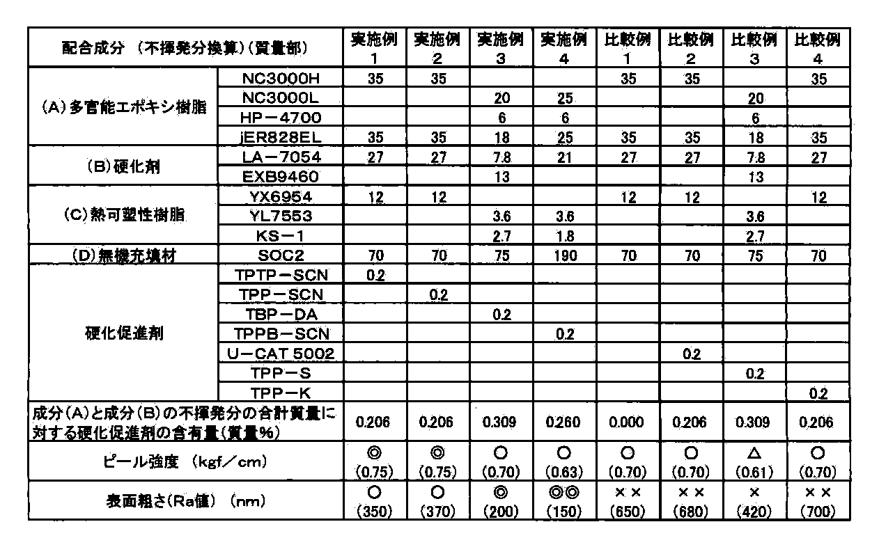
液状ビスフェノールA型エポキシ樹脂(エポキシ当量180、ジャパンエポキシレジン(株)製「jER828EL」)35部と、ビフェニル型エポキシ樹脂(エポキシ当量269、日本化薬(株)製「NC3000H」)35部、フェノキシ樹脂(重量平均分子量38000、ジャパンエポキシレジン(株)製「YX6954」不揮発分30質量%のメチルエチルケトン(以下「MEK」と略称する。)とシクロヘキサノンの1:1溶液)40部とをMEK10部、シクロヘキサノン3部に撹拌しながら加熱溶解させた。そこへ、フェノールノボラック系硬化剤(DIC(株)製「LA−7054」不揮発分60質量%のMEK溶液、フェノール性水酸基当量124)45部、4級ホスホニウム系硬化促進剤である(4−メチルフェニル)トリフェニルホスホニウムチオシアネート(北興化学工業(株)製、「TPTP−SCN」不揮発分10質量%のジメチルホルムアミド(以下「DMF」と略称する。)溶液)2部、球形シリカ(平均粒径0.5μm、アミノシラン処理付「SOC2」アドマテックス社製)70部、高速回転ミキサーで均一に分散して、樹脂ワニスを作製した。次に、かかる樹脂ワニスをポリエチレンテレフタレート(厚さ38μm、以下「PET」と略称する。)上に、乾燥後の樹脂厚みが40μmとなるようにダイコーターにて塗布し、80~120℃(平均100℃)で6分間乾燥した(残留溶媒量約2質量%)。次いで樹脂組成物の表面に厚さ15μmのポリプロピレンフィルムを貼り合わせながらロール状に巻き取った。ロール状の接着フィルムを幅507mmにスリット(slit)し、これより507×336mmサイズのシート状の接着フィルムを得た。
実施例1の4級ホスホニウム系硬化促進剤である(4−メチルフェニル)トリフェニルホスホニウムチオシアネート(北興化学工業(株)製、「TPTP−SCN」不揮発分10質量%のDMF溶液)2部を、同じく4級ホスホニウム系硬化促進剤であるテトラフェニルホスホニウムチオシアネート(北興化学工業(株)製、「TPP−SCN」不揮発分5質量%のDMF溶液)4部に変更する以外は、全く同様にして接着フィルムを得た。次に、かかる樹脂ワニスを使用し、実施例1と全く同様にして接着フィルムを得た。
液状ビスフェノールA型エポキシ樹脂(エポキシ当量180、ジャパンエポキシレジン(株)製「jER828EL」)18部と、ビフェニル型エポキシ樹脂(エポキシ当量269、日本化薬(株)製「NC3000L」)20部、ナフタレン型4官能エポキシ樹脂(エポキシ当量162、DIC(株)製「HP−4700」)6部、フェノキシ樹脂(重量平均分子量38000、ジャパンエポキシレジン(株)製「YL7553」不揮発分30質量%のMEKとシクロヘキサノンの1:1溶液)12部とをMEK8部、シクロヘキサノン8部に撹拌しながら加熱溶解させた。そこへ、フェノールノボラック系硬化剤(DIC(株)製「LA−7054」不揮発分60質量%のMEK溶液、フェノール性水酸基当量124)13部、活性エステル系硬化剤(DIC(株)製「EXB−9460」不揮発分65質量%のトルエン溶液、活性エステル当量223)20部、4級ホスホニウム系硬化促進剤であるテトラブチルホスホニウムデカン酸塩(北興化学工業(株)製、「TBP−DA」)0.2部、球形シリカ(平均粒径0.5μm、アミノシラン処理付「SOC2」アドマテックス社製)75部、ポリビニルブチラール樹脂溶液(ガラス転移温度105℃、積水化学工業(株)製「KS−1」不揮発分15質量%のエタノールとトルエンの1:1溶液)18部を混合し、高速回転ミキサーで均一に分散して、樹脂ワニスを作製した。次に、かかる樹脂ワニスを使用し、実施例1と全く同様にして接着フィルムを得た。
液状ビスフェノールA型エポキシ樹脂(エポキシ当量180、ジャパンエポキシレジン(株)製「jER828EL」)25部と、ビフェニル型エポキシ樹脂(エポキシ当量269、日本化薬(株)製「NC3000L」)25部、ナフタレン型4官能エポキシ樹脂(エポキシ当量162、DIC(株)製「HP−4700」)6部、フェノキシ樹脂(重量平均分子量38000、ジャパンエポキシレジン(株)製「YL7553」不揮発分30質量%のMEKとシクロヘキサノンの1:1溶液)12部とをMEK5部、シクロヘキサノン5部に撹拌しながら加熱溶解させた。そこへ、フェノールノボラック系硬化剤(DIC(株)製「LA−7054」不揮発分60質量%のMEK溶液、フェノール性水酸基当量124)36部、4級ホスホニウム系硬化促進剤であるブチルトリフェニルホスホニウムチオシアネート(北興化学工業(株)製、「TPPB−SCN」不揮発分10質量%のDMF溶液)2部、球形シリカ(平均粒径0.5μm、アミノシラン処理付「SOC2」アドマテックス社製)190部、ポリビニルブチラール樹脂溶液(ガラス転移温度105℃、積水化学工業(株)製「KS−1」不揮発分15質量%のエタノールとトルエンの1:1溶液)12部を混合し、高速回転ミキサーで均一に分散して、樹脂ワニスを作製した。次に、かかる樹脂ワニスを使用し、実施例1と全く同様にして接着フィルムを得た。
実施例1の4級ホスホニウム系硬化促進剤を加えないこと以外は、全く同様にして接着フィルムを得た。次に、かかる樹脂ワニスを使用し、実施例1と全く同様にして接着フィルムを得た。
実施例1の4級ホスホニウム系硬化促進剤である(4−メチルフェニル)トリフェニルホスホニウムチオシアネート(北興化学工業(株)製、「TPTP−SCN」不揮発分10質量%のDMF溶液)2部を、同じく4級ホスホニウム系硬化促進剤であるDBU系テトラフェニルボレート塩(サンアプロ株式会社製、「U−CAT 5002」不揮発分10質量%のMEK溶液)2部に変更する以外は、全く同様にして接着フィルムを得た。次に、かかる樹脂ワニスを使用し、実施例1と全く同様にして接着フィルムを得た。
実施例3の4級ホスホニウム系硬化促進剤であるテトラブチルホスホニウムデカン酸塩(北興化学工業(株)製、「TBP−DA」)0.2部を、同じく4級ホスホニウム系硬化促進剤であるトリフェニルホスフィントリフェニルボラン(北興化学工業(株)製、「TPP−S」不揮発分10質量%のDMF溶液)2部に変更する以外は、全く同様にして接着フィルムを得た。次に、かかる樹脂ワニスを使用し、実施例1と全く同様にして接着フィルムを得た。
実施例1の4級ホスホニウム系硬化促進剤である(4−メチルフェニル)トリフェニルホスホニウムチオシアネート(北興化学工業(株)製、「TPTP−SCN」不揮発分10質量%のDMF溶液)2部を、同じく4級ホスホニウム系硬化促進剤であるテトラフェニルホスホニウムテトラフェニルボレート(北興化学工業(株)製、「TPP−K」)0.2部に変更する以外は、全く同様にして接着フィルムを得た。次に、かかる樹脂ワニスを使用し、実施例1と全く同様にして接着フィルムを得た。
(1)内層回路基板の下地処理
内層回路を形成したガラス布基材エポキシ樹脂両面銅張積層板[銅箔の厚さ18μm、基板厚み0.3mm、松下電工(株)製R5715ES]の両面をメック(株)製CZ8100に浸漬して銅表面の粗化処理をおこなった。
実施例及び比較例で作成した接着フィルムを、バッチ式真空加圧ラミネーターMVLP−500(名機(株)製商品名)を用いて、内層回路基板の両面にラミネートした。ラミネートは、30秒間減圧して気圧を13hPa以下とし、その後30秒間、100℃、圧力0.74MPaでプレスすることにより行った。
ラミネートされた接着フィルムからPETフィルムを剥離し、180℃、30分の硬化条件で樹脂組成物を硬化し絶縁層を形成した。
絶縁層を形成した内層回路基板を、膨潤液である、アトテックジャパン(株)のジエチレングリコールモノブチルエーテル含有のスエリングディップ・セキュリガンドPに60℃で5分間浸漬し、次に粗化液として、アトテックジャパン(株)のコンセントレート・コンパクトP(KMnO4:60g/L、NaOH:40g/Lの水溶液)に80℃で20分間浸漬、最後に中和液として、アトテックジャパン(株)のリダクションショリューシン・セキュリガントPに40℃で5分間浸漬した。この基板を用いて粗化処理後の絶縁層表面の表面粗さ(Ra値)の測定を行った。
絶縁層表面に回路を形成するために、内層回路基板を、PdCl2を含む無電解メッキ用溶液に浸漬し、次に無電解銅メッキ液に浸漬した。150℃にて30分間加熱してアニール処理を行った後に、エッチングレジストを形成し、エッチングによるパターン形成の後に、硫酸銅電解メッキを行い、30±5μmの厚さで導体層を形成した。次に、アニール処理を180℃にて60分間行った。この回路基板についてメッキ導体層のピール強度の測定を行った。
回路基板の導体層に、幅10mm、長さ100mmの切込みをカッターを用いていれ、この一端を剥がしてつかみ具(株式会社ティー・エス・イー、オートコム型試験機 AC−50C−SL)で掴み、室温中にて、50mm/分の速度で垂直方向に35mmを引き剥がした時の荷重を測定した。荷重が0.75kgf/cm以上の場合を「◎」とし、0.75kgf/cm未満0.62kgf/cm以上の場合を「○」とし、0.62kgf/cm未満0.40kgf/cm以上の場合を「△」とし、0.40kgf/cm未満の場合を「×」として評価した。
非接触型表面粗さ計(ビーコインスツルメンツ社製WYKO NT3300)を用いて、VSIコンタクトモード、50倍レンズにより測定範囲を121μm×92μmとして得られる数値を測定した。そして10点の平均の表面粗さを求めることによりRa値とした。Ra値が500nm以上の場合を「××」とし、500nm未満420nm以上の場合を「×」とし、420nm未満380nm以上の場合を「△」とし、380nm未満300nm以上の場合を「○」とし、300nm未満200nm以上の場合を「◎」とし、200nm未満の場合を「◎◎」として評価した。
Claims (9)
- (A)多官能エポキシ樹脂、(B)フェノール系硬化剤及び/又は活性エステル系硬化剤、(C)熱可塑性樹脂、(D)無機充填材、(E)テトラブチルホスホニウムデカン酸塩、(4−メチルフェニル)トリフェニルホスホニウムチオシアネート、テトラフェニルホスホニウムチオシアネート、ブチルトリフェニルホスホニウムチオシアネートから選ばれる1種以上の4級ホスホニウム系硬化促進剤を含有する樹脂組成物。
- 成分(A)と成分(B)の不揮発分の合計質量に対する成分(E)の質量の比率が100:0.05~100:2となる範囲で成分(E)を含む、請求項1記載の樹脂組成物。
- 樹脂組成物中に存在するエポキシ基と成分(B)の硬化剤の反応基の比率がモル比で1:0.3~1:1となる範囲で成分(B)を含む、請求項1又は2記載の樹脂組成物。
- 樹脂組成物の不揮発分を100質量%とした場合、成分(C)の含有量が1~20質量%である、請求項1~3のいずれか1項に記載の樹脂組成物。
- 樹脂組成物の不揮発分を100質量%とした場合、成分(D)の含有量が10~70質量%である請求項1~4のいずれか1項に記載の樹脂組成物。
- ピール強度が0.4kgf/cm~2kgf/cmであり、表面粗さが30nm~400nmであることを特徴とする、請求項1~5のいずれか1項に記載の樹脂組成物。
- 請求項1~6のいずれか1項に記載の樹脂組成物が支持体上に層形成されている接着フィルム。
- 請求項1~6のいずれか1項に記載の樹脂組成物がシート状繊維基材中に含浸されているプリプレグ。
- 請求項1~6のいずれか1項に記載の樹脂組成物の硬化物により絶縁層が形成されている回路基板。
Priority Applications (3)
| Application Number | Priority Date | Filing Date | Title |
|---|---|---|---|
| JP2010548592A JP6027304B2 (ja) | 2009-01-30 | 2010-01-29 | 樹脂組成物 |
| CN201080006427.2A CN102300901B (zh) | 2009-01-30 | 2010-01-29 | 树脂组合物 |
| KR1020117009896A KR101690095B1 (ko) | 2009-01-30 | 2010-01-29 | 수지 조성물 |
Applications Claiming Priority (2)
| Application Number | Priority Date | Filing Date | Title |
|---|---|---|---|
| JP2009019069 | 2009-01-30 | ||
| JP2009-019069 | 2009-01-30 |
Publications (1)
| Publication Number | Publication Date |
|---|---|
| WO2010087526A1 true WO2010087526A1 (ja) | 2010-08-05 |
Family
ID=42395766
Family Applications (1)
| Application Number | Title | Priority Date | Filing Date |
|---|---|---|---|
| PCT/JP2010/051664 Ceased WO2010087526A1 (ja) | 2009-01-30 | 2010-01-29 | 樹脂組成物 |
Country Status (5)
| Country | Link |
|---|---|
| JP (2) | JP6027304B2 (ja) |
| KR (1) | KR101690095B1 (ja) |
| CN (1) | CN102300901B (ja) |
| TW (1) | TWI494364B (ja) |
| WO (1) | WO2010087526A1 (ja) |
Cited By (12)
| Publication number | Priority date | Publication date | Assignee | Title |
|---|---|---|---|---|
| JP2012036339A (ja) * | 2010-08-10 | 2012-02-23 | Hitachi Chem Co Ltd | 樹脂組成物、樹脂硬化物、配線板及び配線板の製造方法 |
| WO2012020713A3 (ja) * | 2010-08-10 | 2012-04-12 | 日立化成工業株式会社 | 樹脂組成物、樹脂硬化物、配線板及び配線板の製造方法 |
| JP2014028880A (ja) * | 2012-07-31 | 2014-02-13 | Ajinomoto Co Inc | 樹脂組成物 |
| KR20160002401A (ko) | 2014-06-30 | 2016-01-07 | 신닛테츠 수미킨 가가쿠 가부시키가이샤 | 방향족 폴리에스테르 함유 경화성 수지 조성물, 경화물, 전기·전자 부품 및 회로 기판 |
| JP2017048400A (ja) * | 2016-11-29 | 2017-03-09 | 味の素株式会社 | 樹脂組成物 |
| JP2017110104A (ja) * | 2015-12-16 | 2017-06-22 | 味の素株式会社 | プリプレグ |
| WO2018043035A1 (ja) * | 2016-08-30 | 2018-03-08 | リンテック株式会社 | 樹脂組成物、樹脂シート、及び半導体装置 |
| WO2018168718A1 (ja) * | 2017-03-14 | 2018-09-20 | 三井金属鉱業株式会社 | 樹脂組成物、樹脂付銅箔、誘電体層、銅張積層板、キャパシタ素子及びキャパシタ内蔵プリント配線板 |
| JP2019011481A (ja) * | 2018-10-30 | 2019-01-24 | 味の素株式会社 | 樹脂組成物 |
| KR20190038859A (ko) | 2016-07-29 | 2019-04-09 | 혹꼬우 가가꾸 고오교오 가부시끼가이샤 | 신규 포스포늄 화합물 |
| KR20190084890A (ko) * | 2018-01-09 | 2019-07-17 | 아지노모토 가부시키가이샤 | 수지 조성물 |
| JP2020139164A (ja) * | 2015-12-16 | 2020-09-03 | 味の素株式会社 | プリプレグ |
Families Citing this family (21)
| Publication number | Priority date | Publication date | Assignee | Title |
|---|---|---|---|---|
| KR101897955B1 (ko) * | 2012-01-23 | 2018-09-12 | 아지노모토 가부시키가이샤 | 수지 조성물 |
| CN102746798B (zh) * | 2012-07-10 | 2014-07-16 | 广东汕头超声电子股份有限公司覆铜板厂 | 一种高导热半固化胶膜及其制备方法 |
| CN102746622A (zh) * | 2012-07-26 | 2012-10-24 | 哈尔滨玻璃钢研究院 | 一种中温固化环氧树脂为基体材料的预浸料及其制备方法 |
| KR101350997B1 (ko) * | 2012-08-21 | 2014-01-14 | 주식회사 신아티앤씨 | 전기적 특성이 우수한 에폭시 화합물 및 그 제조방법 |
| JP6205692B2 (ja) * | 2012-09-03 | 2017-10-04 | 味の素株式会社 | 熱硬化性エポキシ樹脂組成物、絶縁層形成用接着フィルム及び多層プリント配線板 |
| KR101849833B1 (ko) * | 2012-09-14 | 2018-04-17 | 셍기 테크놀로지 코. 엘티디. | 에폭시 수지 조성물 및 상기 조성물을 사용하여 제작된 프리프레그 및 동박적층판 |
| EP2896654B1 (en) * | 2012-09-14 | 2017-07-12 | Shengyi Technology Co. Ltd. | Epoxy resin compound, and, prepreg and copper-clad laminate manufactured using the compound |
| TWI633011B (zh) * | 2012-10-15 | 2018-08-21 | Ajinomoto Co., Inc. | Resin composition |
| JP6308344B2 (ja) * | 2013-04-08 | 2018-04-11 | 味の素株式会社 | 硬化性樹脂組成物 |
| CN103333466B (zh) * | 2013-06-20 | 2015-08-26 | 天津凯华绝缘材料股份有限公司 | 一种具有互穿网络结构的高柔性环氧树脂及其合成方法 |
| CN103589383B (zh) * | 2013-11-03 | 2015-03-25 | 江苏金瀚电子科技发展有限公司 | 软排线用聚酯树脂组合物 |
| KR101577686B1 (ko) * | 2014-12-22 | 2015-12-29 | 주식회사 이녹스 | 다이싱 다이본딩 필름용 접착수지, 이를 포함하는 다이싱 다이본딩 필름용 접착필름 및 다이싱 다이본딩 필름 |
| KR101772871B1 (ko) * | 2016-07-11 | 2017-08-30 | 주식회사 두산 | 안테나 모듈 형성용 복합기판 및 이의 제조방법 |
| KR102649094B1 (ko) | 2016-09-29 | 2024-03-20 | 세키스이가가쿠 고교가부시키가이샤 | 층간 절연 재료 및 다층 프린트 배선판 |
| KR102402868B1 (ko) | 2016-09-29 | 2022-05-27 | 세키스이가가쿠 고교가부시키가이샤 | 경화체 및 다층 기판 |
| JP6915256B2 (ja) * | 2016-10-18 | 2021-08-04 | 昭和電工マテリアルズ株式会社 | 封止用樹脂組成物、並びに、それを用いた再配置ウエハ、半導体パッケージ及び半導体パッケージの製造方法 |
| JP6878859B2 (ja) * | 2016-12-02 | 2021-06-02 | 味の素株式会社 | 樹脂組成物 |
| CN108727942A (zh) * | 2017-04-24 | 2018-11-02 | 味之素株式会社 | 树脂组合物 |
| KR101958322B1 (ko) * | 2017-05-29 | 2019-03-18 | 주식회사 에스씨플러스 | 금속 접착제 조성물 |
| KR102160528B1 (ko) * | 2018-12-27 | 2020-09-28 | 한화글로벌에셋 주식회사 | 저유전 커버레이 필름 및 이를 위한 커버레이 필름용 조성물 |
| JP7472839B2 (ja) * | 2021-03-26 | 2024-04-23 | 味の素株式会社 | 樹脂組成物 |
Citations (6)
| Publication number | Priority date | Publication date | Assignee | Title |
|---|---|---|---|---|
| JP2001098049A (ja) * | 1999-09-29 | 2001-04-10 | Shin Etsu Chem Co Ltd | 半導体封止用液状エポキシ樹脂組成物 |
| JP2001181375A (ja) * | 1999-10-13 | 2001-07-03 | Ajinomoto Co Inc | エポキシ樹脂組成物並びに該組成物を用いた接着フィルム及びプリプレグ、及びこれらを用いた多層プリント配線板及びその製造法 |
| JP2007254710A (ja) * | 2005-11-29 | 2007-10-04 | Ajinomoto Co Inc | 多層プリント配線板の層間絶縁層用樹脂組成物 |
| JP2009062447A (ja) * | 2007-09-06 | 2009-03-26 | Hokko Chem Ind Co Ltd | 液状エポキシ樹脂系組成物 |
| JP2009227962A (ja) * | 2008-02-26 | 2009-10-08 | Panasonic Electric Works Co Ltd | 封止用エポキシ樹脂組成物および半導体装置 |
| JP2009298960A (ja) * | 2008-06-16 | 2009-12-24 | Hokko Chem Ind Co Ltd | 新規なホスホニウムチオシアネート化合物およびエポキシ樹脂用硬化促進剤 |
Family Cites Families (11)
| Publication number | Priority date | Publication date | Assignee | Title |
|---|---|---|---|---|
| JPS6381187A (ja) * | 1986-09-25 | 1988-04-12 | Ibiden Co Ltd | 熱硬化性接着シ−ト |
| JP3290295B2 (ja) * | 1994-05-13 | 2002-06-10 | 太陽インキ製造株式会社 | 硬化性樹脂組成物並びに該組成物を用いた多層プリント配線板及びその製造方法 |
| JPH0832243A (ja) * | 1994-07-18 | 1996-02-02 | Sumitomo Bakelite Co Ltd | 多層プリント配線板の製造方法 |
| JPH10275983A (ja) * | 1997-03-31 | 1998-10-13 | Ibiden Co Ltd | 多層プリント配線板 |
| JP2002161150A (ja) * | 2000-11-28 | 2002-06-04 | Japan Gore Tex Inc | プリプレグおよびこれを用いた積層板およびプリント配線基板 |
| JP4240976B2 (ja) * | 2002-09-27 | 2009-03-18 | 住友ベークライト株式会社 | 硬化促進剤、硬化促進剤の製造方法、エポキシ樹脂組成物および半導体装置 |
| JP4341254B2 (ja) * | 2003-02-06 | 2009-10-07 | 住友ベークライト株式会社 | エポキシ樹脂組成物用硬化促進剤、エポキシ樹脂組成物および半導体装置 |
| JP2006213797A (ja) * | 2005-02-02 | 2006-08-17 | Nippon Paint Co Ltd | 熱硬化性誘電体樹脂組成物及び熱硬化性誘電体樹脂フィルム |
| JP4983228B2 (ja) * | 2005-11-29 | 2012-07-25 | 味の素株式会社 | 多層プリント配線板の絶縁層用樹脂組成物 |
| JP5089560B2 (ja) * | 2008-11-28 | 2012-12-05 | リンテック株式会社 | 半導体チップ積層体および半導体チップ積層用接着剤組成物 |
| JP5195454B2 (ja) * | 2009-01-22 | 2013-05-08 | 味の素株式会社 | 樹脂組成物 |
-
2010
- 2010-01-28 TW TW099102449A patent/TWI494364B/zh active
- 2010-01-29 WO PCT/JP2010/051664 patent/WO2010087526A1/ja not_active Ceased
- 2010-01-29 KR KR1020117009896A patent/KR101690095B1/ko active Active
- 2010-01-29 CN CN201080006427.2A patent/CN102300901B/zh active Active
- 2010-01-29 JP JP2010548592A patent/JP6027304B2/ja active Active
-
2015
- 2015-03-02 JP JP2015040262A patent/JP6267140B2/ja active Active
Patent Citations (6)
| Publication number | Priority date | Publication date | Assignee | Title |
|---|---|---|---|---|
| JP2001098049A (ja) * | 1999-09-29 | 2001-04-10 | Shin Etsu Chem Co Ltd | 半導体封止用液状エポキシ樹脂組成物 |
| JP2001181375A (ja) * | 1999-10-13 | 2001-07-03 | Ajinomoto Co Inc | エポキシ樹脂組成物並びに該組成物を用いた接着フィルム及びプリプレグ、及びこれらを用いた多層プリント配線板及びその製造法 |
| JP2007254710A (ja) * | 2005-11-29 | 2007-10-04 | Ajinomoto Co Inc | 多層プリント配線板の層間絶縁層用樹脂組成物 |
| JP2009062447A (ja) * | 2007-09-06 | 2009-03-26 | Hokko Chem Ind Co Ltd | 液状エポキシ樹脂系組成物 |
| JP2009227962A (ja) * | 2008-02-26 | 2009-10-08 | Panasonic Electric Works Co Ltd | 封止用エポキシ樹脂組成物および半導体装置 |
| JP2009298960A (ja) * | 2008-06-16 | 2009-12-24 | Hokko Chem Ind Co Ltd | 新規なホスホニウムチオシアネート化合物およびエポキシ樹脂用硬化促進剤 |
Cited By (21)
| Publication number | Priority date | Publication date | Assignee | Title |
|---|---|---|---|---|
| WO2012020713A3 (ja) * | 2010-08-10 | 2012-04-12 | 日立化成工業株式会社 | 樹脂組成物、樹脂硬化物、配線板及び配線板の製造方法 |
| CN103140537A (zh) * | 2010-08-10 | 2013-06-05 | 日立化成株式会社 | 树脂组合物、树脂固化物、配线板及配线板的制造方法 |
| CN103140537B (zh) * | 2010-08-10 | 2016-10-12 | 日立化成株式会社 | 树脂组合物、树脂固化物、配线板及配线板的制造方法 |
| JP2012036339A (ja) * | 2010-08-10 | 2012-02-23 | Hitachi Chem Co Ltd | 樹脂組成物、樹脂硬化物、配線板及び配線板の製造方法 |
| JP2014028880A (ja) * | 2012-07-31 | 2014-02-13 | Ajinomoto Co Inc | 樹脂組成物 |
| KR20160002401A (ko) | 2014-06-30 | 2016-01-07 | 신닛테츠 수미킨 가가쿠 가부시키가이샤 | 방향족 폴리에스테르 함유 경화성 수지 조성물, 경화물, 전기·전자 부품 및 회로 기판 |
| JP2017110104A (ja) * | 2015-12-16 | 2017-06-22 | 味の素株式会社 | プリプレグ |
| JP2020139164A (ja) * | 2015-12-16 | 2020-09-03 | 味の素株式会社 | プリプレグ |
| KR20190038859A (ko) | 2016-07-29 | 2019-04-09 | 혹꼬우 가가꾸 고오교오 가부시끼가이샤 | 신규 포스포늄 화합물 |
| JPWO2018043035A1 (ja) * | 2016-08-30 | 2019-06-24 | リンテック株式会社 | 樹脂組成物、樹脂シート、及び半導体装置 |
| WO2018043035A1 (ja) * | 2016-08-30 | 2018-03-08 | リンテック株式会社 | 樹脂組成物、樹脂シート、及び半導体装置 |
| JP2017048400A (ja) * | 2016-11-29 | 2017-03-09 | 味の素株式会社 | 樹脂組成物 |
| JPWO2018168718A1 (ja) * | 2017-03-14 | 2020-01-16 | 三井金属鉱業株式会社 | 樹脂組成物、樹脂付銅箔、誘電体層、銅張積層板、キャパシタ素子及びキャパシタ内蔵プリント配線板 |
| WO2018168718A1 (ja) * | 2017-03-14 | 2018-09-20 | 三井金属鉱業株式会社 | 樹脂組成物、樹脂付銅箔、誘電体層、銅張積層板、キャパシタ素子及びキャパシタ内蔵プリント配線板 |
| JP7013444B2 (ja) | 2017-03-14 | 2022-01-31 | 三井金属鉱業株式会社 | 樹脂組成物、樹脂付銅箔、誘電体層、銅張積層板、キャパシタ素子及びキャパシタ内蔵プリント配線板 |
| US11310910B2 (en) | 2017-03-14 | 2022-04-19 | Mitsui Mining & Smelting Co., Ltd. | Resin composition, copper foil with resin, dielectric layer, copper clad laminate sheet, capacitor element and printed wiring board with built-in capacitor |
| KR20190084890A (ko) * | 2018-01-09 | 2019-07-17 | 아지노모토 가부시키가이샤 | 수지 조성물 |
| JP2019119819A (ja) * | 2018-01-09 | 2019-07-22 | 味の素株式会社 | 樹脂組成物 |
| JP7296191B2 (ja) | 2018-01-09 | 2023-06-22 | 味の素株式会社 | 硬化性樹脂組成物、樹脂シート、プリント配線板及び半導体装置 |
| KR102752113B1 (ko) | 2018-01-09 | 2025-01-10 | 아지노모토 가부시키가이샤 | 수지 조성물 |
| JP2019011481A (ja) * | 2018-10-30 | 2019-01-24 | 味の素株式会社 | 樹脂組成物 |
Also Published As
| Publication number | Publication date |
|---|---|
| JP2015145498A (ja) | 2015-08-13 |
| JP6027304B2 (ja) | 2016-11-16 |
| KR20110124198A (ko) | 2011-11-16 |
| KR101690095B1 (ko) | 2016-12-27 |
| JPWO2010087526A1 (ja) | 2012-08-09 |
| TWI494364B (zh) | 2015-08-01 |
| TW201031707A (en) | 2010-09-01 |
| CN102300901B (zh) | 2014-07-30 |
| JP6267140B2 (ja) | 2018-01-24 |
| CN102300901A (zh) | 2011-12-28 |
Similar Documents
| Publication | Publication Date | Title |
|---|---|---|
| JP6267140B2 (ja) | 樹脂組成物 | |
| JP6024783B2 (ja) | 樹脂組成物 | |
| JP4983228B2 (ja) | 多層プリント配線板の絶縁層用樹脂組成物 | |
| JP5505435B2 (ja) | 多層プリント配線板の絶縁層用樹脂組成物 | |
| JP5573869B2 (ja) | 多層プリント配線板の層間絶縁層用樹脂組成物 | |
| JP4992396B2 (ja) | 多層プリント配線板の層間絶縁層用樹脂組成物 | |
| JP5195454B2 (ja) | 樹脂組成物 | |
| JP5651941B2 (ja) | エポキシ樹脂組成物 | |
| JP6123169B2 (ja) | 樹脂組成物 | |
| JP5396805B2 (ja) | エポキシ樹脂組成物 | |
| JP5249903B2 (ja) | 樹脂組成物 | |
| JP5408046B2 (ja) | 樹脂組成物 | |
| JP5446866B2 (ja) | エポキシ樹脂組成物 | |
| JP2013234328A (ja) | エポキシ樹脂組成物 | |
| JP6007663B2 (ja) | 樹脂組成物 | |
| WO2007097209A1 (ja) | エポキシ樹脂組成物 | |
| JP5904256B2 (ja) | 樹脂組成物 | |
| JP6534986B2 (ja) | 樹脂組成物 | |
| JP6269401B2 (ja) | 表面処理無機充填材、該無機充填材の製造方法、および該無機充填材を含有する樹脂組成物 | |
| JP5644823B2 (ja) | 樹脂組成物 | |
| JP2011246406A (ja) | 有機けい素化合物 | |
| JP6337917B2 (ja) | 樹脂組成物 |
Legal Events
| Date | Code | Title | Description |
|---|---|---|---|
| WWE | Wipo information: entry into national phase |
Ref document number: 201080006427.2 Country of ref document: CN |
|
| 121 | Ep: the epo has been informed by wipo that ep was designated in this application |
Ref document number: 10735975 Country of ref document: EP Kind code of ref document: A1 |
|
| ENP | Entry into the national phase |
Ref document number: 20117009896 Country of ref document: KR Kind code of ref document: A |
|
| WWE | Wipo information: entry into national phase |
Ref document number: 2010548592 Country of ref document: JP |
|
| NENP | Non-entry into the national phase |
Ref country code: DE |
|
| 122 | Ep: pct application non-entry in european phase |
Ref document number: 10735975 Country of ref document: EP Kind code of ref document: A1 |