WO2010079804A1 - 電子部品 - Google Patents
電子部品 Download PDFInfo
- Publication number
- WO2010079804A1 WO2010079804A1 PCT/JP2010/050098 JP2010050098W WO2010079804A1 WO 2010079804 A1 WO2010079804 A1 WO 2010079804A1 JP 2010050098 W JP2010050098 W JP 2010050098W WO 2010079804 A1 WO2010079804 A1 WO 2010079804A1
- Authority
- WO
- WIPO (PCT)
- Prior art keywords
- coil
- electronic component
- point
- conductors
- conductor
- Prior art date
- Legal status (The legal status is an assumption and is not a legal conclusion. Google has not performed a legal analysis and makes no representation as to the accuracy of the status listed.)
- Ceased
Links
Images



Classifications
-
- H—ELECTRICITY
- H01—ELECTRIC ELEMENTS
- H01F—MAGNETS; INDUCTANCES; TRANSFORMERS; SELECTION OF MATERIALS FOR THEIR MAGNETIC PROPERTIES
- H01F17/00—Fixed inductances of the signal type
-
- H—ELECTRICITY
- H01—ELECTRIC ELEMENTS
- H01F—MAGNETS; INDUCTANCES; TRANSFORMERS; SELECTION OF MATERIALS FOR THEIR MAGNETIC PROPERTIES
- H01F17/00—Fixed inductances of the signal type
- H01F17/0006—Printed inductances
- H01F17/0013—Printed inductances with stacked layers
-
- H—ELECTRICITY
- H01—ELECTRIC ELEMENTS
- H01F—MAGNETS; INDUCTANCES; TRANSFORMERS; SELECTION OF MATERIALS FOR THEIR MAGNETIC PROPERTIES
- H01F27/00—Details of transformers or inductances, in general
- H01F27/28—Coils; Windings; Conductive connections
-
- H—ELECTRICITY
- H01—ELECTRIC ELEMENTS
- H01F—MAGNETS; INDUCTANCES; TRANSFORMERS; SELECTION OF MATERIALS FOR THEIR MAGNETIC PROPERTIES
- H01F17/00—Fixed inductances of the signal type
- H01F17/0006—Printed inductances
- H01F17/0013—Printed inductances with stacked layers
- H01F2017/002—Details of via holes for interconnecting the layers
-
- H—ELECTRICITY
- H01—ELECTRIC ELEMENTS
- H01F—MAGNETS; INDUCTANCES; TRANSFORMERS; SELECTION OF MATERIALS FOR THEIR MAGNETIC PROPERTIES
- H01F17/00—Fixed inductances of the signal type
- H01F17/0006—Printed inductances
- H01F2017/0073—Printed inductances with a special conductive pattern, e.g. flat spiral
-
- H—ELECTRICITY
- H01—ELECTRIC ELEMENTS
- H01F—MAGNETS; INDUCTANCES; TRANSFORMERS; SELECTION OF MATERIALS FOR THEIR MAGNETIC PROPERTIES
- H01F27/00—Details of transformers or inductances, in general
- H01F27/28—Coils; Windings; Conductive connections
- H01F27/29—Terminals; Tapping arrangements for signal inductances
- H01F27/292—Surface mounted devices
Definitions
- the present invention relates to an electronic component, and more particularly to an electronic component having a built-in coil.
- FIG. 8 is a plan view of ceramic green sheets 202a and 202b used in the multilayer electronic component.
- ceramic green sheets 202a shown in FIG. 8 (a) and ceramic green sheets 202b shown in FIG. 8 (b) are alternately laminated.
- the ceramic green sheets 202a and 202b are provided with coil conductors 204a and 204b, respectively.
- the coil conductors 204a and 204b have a length of one turn and have ends 206a, 208a, 206b, and 208b.
- the ceramic green sheets 202a and 202b are alternately stacked.
- the end portion 206a is connected to the end portion 206b of the coil conductor 204b provided on the upper side in the stacking direction via a via-hole conductor.
- the end 208a is connected to the end 208b of the coil conductor 204b provided on the lower side in the stacking direction via a via-hole conductor.
- the coil which consists of several coil conductors 204a and 204b is comprised.
- the multilayer electronic component described in Patent Document 1 has a problem that it is difficult to obtain a large inductance value. More specifically, in the multilayer electronic component, each of the coil conductors 204a and 204b has a length of one turn. Therefore, in order to connect the coil conductors 204a and 204b without short-circuiting, the end portions 208a and 208b need to be positioned in a rectangular region E1 surrounded by the coil conductors 204a and 204b.
- the end 208b is moved in the direction of arrow a in FIG. Thereby, since the area of the area
- the end 208b is moved in the direction of the arrow a, a short circuit may occur in the coil conductor 204b as will be described below. More specifically, the coil conductor 204b in the vicinity of the end portion 208b and the coil conductor 204b in the vicinity of the end portion 206b extend in parallel in a close state. For this reason, when bleeding occurs during screen printing of the coil conductor 204b, the coil conductor 204b near the end 208b and the coil conductor 204b near the end 206b may be short-circuited. Therefore, it is difficult to largely move the end portion 208b in the direction of the arrow a.
- an object of the present invention is to increase an inductance value while suppressing occurrence of a short circuit in a coil conductor in an electronic component incorporating a coil made of a coil conductor having a length of one turn.
- the electronic component includes a laminated body in which a plurality of insulator layers are laminated, and a coil built in the laminated body, and the coil has a rectangular shape.
- a coil portion having a structure in which one side is cut off at one corner of the annular linear electrode, and a first point located at one end of the coil portion and the first point
- a connecting portion connecting a second point located in a direction making an obtuse angle with respect to the one side inside the region surrounded by the coil portion, and a length of one turn
- a plurality of via-hole conductors connecting the plurality of coil conductors, and the center line of the connection portion includes the first point and the second point. Is a rectangle whose diagonal is a straight line connecting the two, and by a side parallel to the linear electrode It than rectangle made passes through the inner region, characterized by.
- an inductance value can be increased while suppressing occurrence of a short circuit in the coil conductor.
- FIG. 1 is an external perspective view of an electronic component according to an embodiment of the present invention. It is a disassembled perspective view of the laminated body of the electronic component of FIG.
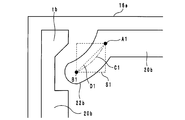
- FIG. 3 is an enlarged view of the connecting portion.
- FIG. 4A is a schematic diagram of a magnetic layer of the electronic component according to the embodiment, and FIGS. 4B and 4C illustrate the electrons according to the first comparative example and the second comparative example.
- It is a schematic diagram of the magnetic body layer of components (equivalent to the conventional electronic component). It is the graph which showed the result of computer simulation. It is the figure which showed the magnetic body layer of the electronic component which concerns on a 1st modification. It is the figure which showed the magnetic body layer of the electronic component which concerns on a 2nd modification. It is the figure which planarly viewed the ceramic green sheet used for the multilayer electronic component described in Patent Document 1.
- FIG. 1 is an external perspective view of an electronic component 10 according to an embodiment.
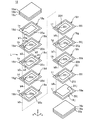
- FIG. 2 is an exploded perspective view of the multilayer body 12 of the electronic component 10 according to the embodiment.
- the stacking direction of the electronic component 10 is defined as the z-axis direction
- the direction along the long side of the electronic component 10 is defined as the x-axis direction
- the direction along the short side of the electronic component 10 is defined as the y-axis direction.
- the x axis, the y axis, and the z axis are orthogonal to each other.
- the electronic component 10 includes a laminate 12, external electrodes 14a and 14b, and a coil L as shown in FIG.
- the laminated body 12 has a rectangular parallelepiped shape and incorporates a coil L.
- the external electrodes 14a and 14b are provided so as to cover side surfaces located on the negative direction side and the positive direction side in the x-axis direction, respectively.
- the laminated body 12 is configured by laminating magnetic layers 16a to 16p so that they are arranged in this order in the z-axis direction.
- alphabets are appended to the reference numerals, and when these are collectively referred to, the alphabets after the reference numerals are omitted.
- the magnetic layer 16 is a rectangular insulator layer made of ferromagnetic ferrite.
- the magnetic layer 16 is made of Ni—Cu—Zn ferrite.
- the coil L is a spiral coil that advances in the z-axis direction while rotating as shown in FIG. As shown in FIG. 2, the coil L includes coil conductors 18a to 18j and via-hole conductors b1 to b9.
- the individual coil conductors 18 alphabets are appended to the reference numerals, and when these are collectively referred to, the alphabets after the reference numerals are omitted.
- the coil conductors 18a to 18j are electrically connected by via-hole conductors b1 to b9 in the multilayer body 12 to constitute a coil L.
- the coil conductors 18b to 18i include coil portions 20b to 20i and connection portions 22b to 22i, respectively, and circulate on the magnetic layers 16e to 16l with a length of one turn.
- the coil conductors 18b to 18i will be described in more detail.
- the coil conductors 18b, 18d, 18f, and 18h have the same structure, and the coil conductors 18c, 18e, 18g, and 18i have the same structure. Therefore, hereinafter, the coil conductor 18b and the coil conductor 18c will be described as examples, and description of the other coil conductors 18 is omitted.
- the coil portion 20b is an annular linear electrode having a rectangular shape as shown in FIG.
- the coil portion 20b has a structure in which one side of two sides constituting the corner is cut out at one corner of the rectangle.
- a notch is provided by configuring one long side s1 to be shorter than the other long side s2.
- the connection portion 22b is a linear electrode connected to one end portion (clockwise upstream end portion) of the coil portion 20b, and extends toward a rectangular region surrounded by the coil portion 20b. is doing.
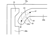
- the connecting portion 22b will be described in more detail with reference to FIG. 3A is an enlarged view of the connection portion 22b, and FIG. 3B is an enlarged view of the connection portion 22c.
- the connecting portion 22b connects the points A1 and B1 located at one end of the coil portion 20b.
- Point B1 is a point located in a direction that forms an obtuse angle ⁇ 1 with respect to long side s1 inside the region surrounded by coil portion 20b when viewed from point A1.
- the center line C1 of the connecting portion 22b is a rectangle S1 having a diagonal line D1 as a straight line connecting the point A1 and the point B1, and includes a side parallel to the linear electrode constituting the coil portion 20b. It passes through an area inside the rectangle S1.
- the center line C1 of the connecting portion 22b connects the point A1 and the point B1 with a straight line and overlaps the diagonal line D1.
- the coil portion 20c is an annular linear electrode having a rectangular shape as shown in FIG.
- the coil portion 20c has a structure in which one side of two sides constituting the corner is cut out at one corner of the rectangle.
- a notch is provided by configuring one short side s3 to be shorter than the other short side s4.
- the connection portion 22c is a linear electrode connected to one end portion (the end portion on the downstream side in the clockwise direction) of the coil portion 20c, and extends toward a rectangular region surrounded by the coil portion 20c. is doing.
- the connecting portion 22c will be described in more detail with reference to FIG.
- the connecting portion 22c connects the point A2 and the point B2 located at one end of the coil portion 20c.
- Point B2 is a point located in a direction forming an obtuse angle ⁇ 2 with respect to the short side s3 inside the region surrounded by the coil portion 20c when viewed from the point A2.
- the center line C2 of the connection part 22c is the rectangle S2 which makes the diagonal line D2 the straight line which connects the point A2 and the point B2, Comprising: It is comprised by the side parallel to the linear electrode which comprises the coil part 20c. It passes through a region inside the rectangle S2.
- the center line C2 of the connecting portion 22c connects the point A2 and the point B2 with a straight line and overlaps the diagonal line D2.
- the end portion tc of the coil portion 20c overlaps the end portion tb of the coil portion 20b when viewed in plan from the z-axis direction.
- the connection part 22c has overlapped with the connection part 22b when planarly viewed from the z-axis direction.
- the coil conductor 18a includes a coil portion 20a and a lead portion 24a, and is provided on the magnetic layer 16d by a conductive material made of Ag.
- the coil portion 20a circulates with a length of 3/4 turns.
- the lead portion 24a is provided at one end of the coil portion 20a, and as shown in FIG. 2, is drawn to the side on the negative direction side in the x-axis direction of the magnetic layer 16d. Further, the end portion ta of the coil portion overlaps the end portion tb of the coil portion 20b when viewed in plan from the z-axis direction.
- the coil conductor 18j includes a coil portion 20j and a lead portion 24j, and is provided on the magnetic layer 16m by a conductive material made of Ag.
- the coil portion 20j circulates with a length of 3/4 turns.
- the lead portion 24j is provided at one end of the coil portion 20j, and is drawn to the side on the positive side in the x-axis direction of the magnetic layer 16m as shown in FIG. Further, the end tj of the coil part overlaps with the end ti of the coil part 20i when viewed in plan from the z-axis direction.
- the via-hole conductors b1 to b9 constitute a part of the spiral coil L by electrically connecting the coil conductors 18a to 18j. More specifically, as shown in FIG. 2, the via-hole conductor b1 penetrates through the magnetic layer 16d to connect the end portion ta and the end portion tb adjacent in the z-axis direction. The via-hole conductor b2 passes through the magnetic layer 16e, thereby connecting the connection part 22b and the connection part 22c adjacent in the z-axis direction. The via-hole conductor b3 passes through the magnetic layer 16f and connects the end tc and the end td adjacent in the z-axis direction.
- the via-hole conductor b4 passes through the magnetic layer 16g to connect the connection portion 22d and the connection portion 22e that are adjacent in the z-axis direction.
- the via-hole conductor b5 connects the end portion te and the end portion tf adjacent in the z-axis direction by penetrating the magnetic layer 16h.
- the via-hole conductor b6 passes through the magnetic layer 16i to connect the connection portion 22f and the connection portion 22g adjacent in the z-axis direction.
- the via-hole conductor b7 penetrates the magnetic layer 16j and connects the end tg and the end th adjacent to each other in the z-axis direction.
- the via-hole conductor b8 penetrates the magnetic layer 16k, thereby connecting the connection part 22h and the connection part 22i adjacent in the z-axis direction.
- the via-hole conductor b9 passes through the magnetic layer 16l and connects the end ti and the end tj that are adjacent in the z-axis direction.
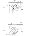
- FIG. 4A is a schematic view of the magnetic layer 16e of the electronic component 10
- FIGS. 4B and 4C illustrate the electronic component (the first comparative example and the second comparative example)
- FIG. 4A the structure of the coil conductor 18b is simplified for easy understanding.
- connection portion 122b extends in a direction perpendicular to the coil portion 120b as in the electronic component according to the first comparative example
- the region E4 surrounded by the connection portion 122 and the coil portion 120 is As shown in 4 (b), it becomes a rectangle.
- the presence of the region E4 prevents the inductance value of the electronic component from being increased. Therefore, it is desirable to make the region E4 as small as possible.
- the connection portion 222b is provided near the coil portion 220b.
- the region E5 becomes smaller than the region E4.
- the inductance value of the electronic component according to the second comparative example is larger than the inductance value of the electronic component according to the first comparative example.
- the electronic component according to the second comparative example has a problem that a short circuit is likely to occur between the coil portion 220b and the connection portion 222b. More specifically, the coil conductor 218b is formed by applying a conductive paste by screen printing. Therefore, at the time of screen printing, the outer edge of the coil conductor 218b may be blurred. And when the space
- the connecting portion 22b is connected to the coil portion 20b when viewed from the point A1 and the point A1 located at one end of the coil portion 20b.
- a point B1 located in a direction that forms an obtuse angle ⁇ 1 with respect to the long side s1 inside the enclosed region is connected.
- the center line C1 of the connection part 22b has connected the point A1 and the point B1 linearly.
- the inductance value of the electronic component 10 is larger than the inductance value of the electronic component according to the first comparative example.
- the electronic component 10 is close to the coil portion 20b only at the tip of the connection portion 22b. Therefore, the distance between the connection part 22b and the coil part 20b in the electronic component 10 is the distance between the connection part 222b and the coil part 220b in the electronic component according to the second comparative example. Smaller than. As a result, in the electronic component 10, the possibility that the connecting portion 22b and the coil portion 20b are short-circuited due to bleeding during screen printing is lower than in the electronic component according to the second comparative example. As described above, in the electronic component 10, it is possible to achieve both an increase in inductance and prevention of a short circuit between the coil portion 20 and the connection portion 22.
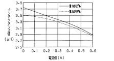
- FIG. 5 is a graph showing the results of computer simulation.
- the vertical axis represents the inductance value
- the horizontal axis represents the current value.
- FIG. 5 shows that the inductance value of the first model is always larger than that of the second model. Therefore, it can be seen that the electronic component 10 can obtain a larger inductance value than the electronic component according to the first comparative example.
- FIG. 6 is a diagram illustrating the magnetic layer 16e of the electronic component 10 according to the first modification.
- FIG. 7 is a diagram illustrating the magnetic layer 16e of the electronic component 10 according to the second modification.
- the center line C1 of the connecting portion 22b does not connect the point A1 and the point B1 linearly but connects the point A1 and the point B1 in a curved state. More specifically, in FIG. 6, the center line C1 of the connection portion 22b is curved so as to swell in the opposite direction to the center direction of the coil portion 20b, and in FIG. 7, the center line C1 of the connection portion 22b is It is curved so as to swell in the central direction of the coil portion 20b. Even in the electronic component 10 having the structure shown in FIGS. 6 and 7, it is possible to achieve both an increase in inductance and prevention of a short circuit between the coil portion 20 and the connection portion 22. However, the center line C1 of the connection part 22b needs to be located inside the rectangle S1.
- the area of the quantity region surrounded by the coil portion and the connection portion 22 is smaller than that of the electronic component 10 shown in FIG. Therefore, the electronic component 10 shown in FIG. 6 can obtain a larger inductance value.
- the average distance between the coil portion 20b and the connection portion 22b is larger than that of the electronic component 10 shown in FIG. Therefore, in the electronic component 10 shown in FIG. 7, a short circuit between the coil portion 20b and the connection portion 22b can be effectively prevented.
- the area of the region surrounded by the coil portion 20b and the connection portion 22b is larger than that of the electronic component 10 shown in FIG. Therefore, in the electronic component 10 shown in FIG. 7, the end tb can be enlarged, and the via-hole conductor b1 and the end tb of the coil portion 20b can be more reliably connected.
- a ceramic green sheet to be the magnetic layer 16 is produced by the following process.
- Ferric oxide (Fe 2 O 3 ), zinc oxide (ZnO), nickel oxide (NiO), and copper oxide (CuO) are weighed at a predetermined ratio, and each material is put into a ball mill as a raw material. Mix. The obtained mixture is dried and pulverized, and the obtained powder is calcined at 750 ° C. for 1 hour. The obtained calcined powder is wet pulverized by a ball mill, dried and then crushed to obtain a ferromagnetic ferrite ceramic powder.
- via-hole conductors b1 to b9 are formed in the ceramic green sheets to be the magnetic layers 16d to 16l, respectively. Specifically, via holes are formed by irradiating the ceramic green sheets to be the magnetic layers 16d to 16l with a laser beam. Next, the via hole is filled with a conductive paste such as Ag, Pd, Cu, Au or an alloy thereof by a method such as printing.
- a conductive paste such as Ag, Pd, Cu, Au or an alloy thereof by a method such as printing.
- a conductive paste mainly composed of Ag, Pd, Cu, Au, or an alloy thereof is applied on the ceramic green sheets to be the magnetic layers 16d to 16m by a screen printing method, whereby the coil conductor 18a. ⁇ 18j are formed.
- the via-hole conductor may be filled with a conductive paste simultaneously with the formation of the coil conductors 18a to 18j.
- these ceramic green sheets are laminated so that the magnetic layers 16a to 16p are arranged in this order from the positive side in the z-axis direction. More specifically, a ceramic green sheet to be the magnetic layer 16p is disposed. Next, the ceramic green sheet to be the magnetic layer 16o is placed and temporarily pressed onto the ceramic green sheet to be the magnetic layer 16p. Thereafter, the ceramic green sheets to be the magnetic layers 16n, 16m, 16l, 16k, 16j, 16i, 16h, 16g, 16f, 16e, 16d, 16c, 16b, and 16a are similarly laminated and temporarily pressed in this order. To obtain a mother laminate. Further, the mother laminate is subjected to main pressure bonding by a hydrostatic pressure press or the like.
- the mother laminated body is cut into a laminated body 12 having a predetermined size by pressing and the unfired laminated body 12 is obtained.
- the unfired laminate 12 is subjected to binder removal processing and firing.
- the binder removal treatment is performed, for example, in a low oxygen atmosphere at 260 ° C. for 3 hours. Firing is performed, for example, at 900 ° C. for 2.5 hours.
- the fired laminated body 12 is obtained through the above steps.
- the laminated body 12 is chamfered by barrel processing.
- a silver electrode to be the external electrodes 14a and 14b is formed on the surface of the laminate 12 by applying and baking an electrode paste whose main component is silver by a method such as an immersion method.
- the silver electrode is dried at 120 ° C. for 15 minutes, and the silver electrode is baked at 700 ° C. for 1 hour.
- the external electrodes 14a and 14b are formed by performing Ni plating / Sn plating on the surface of the silver electrode.
- the present invention is useful for an electronic component, and in particular, in an electronic component incorporating a coil made of a coil conductor having a length of one turn, an inductance value is increased while suppressing occurrence of a short circuit in the coil conductor. It is excellent in that it can be made.
Landscapes
- Engineering & Computer Science (AREA)
- Power Engineering (AREA)
- Microelectronics & Electronic Packaging (AREA)
- Coils Or Transformers For Communication (AREA)
Abstract
Description
以下に、本発明の一実施形態に係る電子部品10について図面を参照しながら説明する。図1は、一実施形態に係る電子部品10の外観斜視図である。図2は、一実施形態に係る電子部品10の積層体12の分解斜視図である。以下、電子部品10の積層方向をz軸方向と定義し、電子部品10の長辺に沿った方向をx軸方向と定義し、電子部品10の短辺に沿った方向をy軸方向と定義する。x軸、y軸及びz軸は互いに直交している。
以上のような電子部品10によれば、以下に説明するように、コイル導体18内において短絡が発生することを抑制しつつ、インダクタンス値を増加させることができる。以下に、図面を参照しながら説明する。図4(a)は、電子部品10の磁性体層16eの模式図であり、図4(b)及び図4(c)は、第1の比較例及び第2の比較例に係る電子部品(従来の電子部品に相当)の磁性体層116e,216eの模式図である。図4(a)では、理解の容易のために、コイル導体18bの構造を簡素化して記載した。
本発明に係る電子部品は、前記電子部品10に示したものに限らず、その要旨の範囲内において、変更可能である。以下に、変形例に係る電子部品10について図面を参照しながら説明する。図6は、第1の変形例に係る電子部品10の磁性体層16eを示した図である。図7は、第2の変形例に係る電子部品10の磁性体層16eを示した図である。
以下に、電子部品10の製造方法について図1及び図2を参照しながら説明する。
C1,C2 中心線
L コイル
S1,S2 長方形
b1~b9 ビアホール導体
s1,s2 長辺
s3,s4 短辺
ta~tj 端部
10 電子部品
12 積層体
14a,14b 外部電極
16a~16p 磁性体層
18a~18j コイル導体
20a~20j コイル部
22b~22i 接続部
24a,24j 引き出し部
Claims (3)
- 複数の絶縁体層が積層されてなる積層体と、
前記積層体に内蔵されているコイルと、
を備えており、
前記コイルは、
長方形状を有する環状の線状電極の一つの角において一方の辺が切り欠かれた構造を有するコイル部、及び、該コイル部の一方の端部に位置する第1の点と該第1の点から見て該コイル部に囲まれた領域の内側において該一方の辺に対して鈍角をなす方向に位置している第2の点とを接続している接続部を有し、かつ、1ターンの長さを有している複数のコイル導体と、
前記複数のコイル導体を接続する複数のビアホール導体と、
を含んでおり、
前記接続部の中心線は、前記第1の点と前記第2の点とを接続する直線を対角線とする長方形であって、前記線状電極に平行な辺により構成される長方形よりも内側の領域を通過していること、
を特徴とする電子部品。 - 前記接続部の中心線は、前記第1の点と前記第2の点とを直線で繋いでいること、
を特徴とする請求項1に記載の電子部品。 - 前記ビアホール導体は、
積層方向に隣り合っている前記コイル部の他方の端部同士を接続している第1のビアホール導体と、
積層方向に隣り合っている前記接続部同士を接続している第2のビアホール導体と、
からなっていること、
を特徴とする請求項1又は請求項2のいずれかに記載の電子部品。
Priority Applications (4)
| Application Number | Priority Date | Filing Date | Title |
|---|---|---|---|
| CN2010800042358A CN102272867A (zh) | 2009-01-08 | 2010-01-07 | 电子元器件 |
| KR1020117013103A KR101296694B1 (ko) | 2009-01-08 | 2010-01-07 | 전자 부품 |
| JP2010545778A JP5573680B2 (ja) | 2009-01-08 | 2010-01-07 | 電子部品 |
| US13/168,692 US8362865B2 (en) | 2009-01-08 | 2011-06-24 | Electronic component |
Applications Claiming Priority (2)
| Application Number | Priority Date | Filing Date | Title |
|---|---|---|---|
| JP2009002159 | 2009-01-08 | ||
| JP2009-002159 | 2009-01-08 |
Related Child Applications (1)
| Application Number | Title | Priority Date | Filing Date |
|---|---|---|---|
| US13/168,692 Continuation US8362865B2 (en) | 2009-01-08 | 2011-06-24 | Electronic component |
Publications (1)
| Publication Number | Publication Date |
|---|---|
| WO2010079804A1 true WO2010079804A1 (ja) | 2010-07-15 |
Family
ID=42316569
Family Applications (1)
| Application Number | Title | Priority Date | Filing Date |
|---|---|---|---|
| PCT/JP2010/050098 Ceased WO2010079804A1 (ja) | 2009-01-08 | 2010-01-07 | 電子部品 |
Country Status (5)
| Country | Link |
|---|---|
| US (1) | US8362865B2 (ja) |
| JP (1) | JP5573680B2 (ja) |
| KR (1) | KR101296694B1 (ja) |
| CN (1) | CN102272867A (ja) |
| WO (1) | WO2010079804A1 (ja) |
Cited By (2)
| Publication number | Priority date | Publication date | Assignee | Title |
|---|---|---|---|---|
| JP2019114768A (ja) * | 2017-12-20 | 2019-07-11 | サムソン エレクトロ−メカニックス カンパニーリミテッド. | コイル電子部品 |
| JP2020047894A (ja) * | 2018-09-21 | 2020-03-26 | Tdk株式会社 | 積層コイル部品 |
Families Citing this family (10)
| Publication number | Priority date | Publication date | Assignee | Title |
|---|---|---|---|---|
| JP5585453B2 (ja) * | 2009-02-02 | 2014-09-10 | 株式会社村田製作所 | 積層インダクタ |
| WO2013128702A1 (ja) * | 2012-02-29 | 2013-09-06 | 株式会社村田製作所 | 積層型インダクタおよび電源回路モジュール |
| KR101532148B1 (ko) * | 2013-11-14 | 2015-06-26 | 삼성전기주식회사 | 적층형 인덕터 |
| CN104733153B (zh) * | 2015-03-30 | 2017-01-18 | 昆山龙腾光电有限公司 | 叠层片式磁珠 |
| KR101883043B1 (ko) * | 2016-02-19 | 2018-07-27 | 삼성전기주식회사 | 코일 부품 |
| US10923259B2 (en) * | 2016-07-07 | 2021-02-16 | Samsung Electro-Mechanics Co., Ltd. | Coil component |
| KR102632344B1 (ko) * | 2016-08-09 | 2024-02-02 | 삼성전기주식회사 | 코일 부품 |
| JP6780589B2 (ja) * | 2017-06-02 | 2020-11-04 | 株式会社村田製作所 | 電子部品 |
| JP6955376B2 (ja) * | 2017-06-16 | 2021-10-27 | 太陽誘電株式会社 | コイル部品及びコイル部品の製造方法 |
| JP7015650B2 (ja) | 2017-07-03 | 2022-02-03 | 太陽誘電株式会社 | コイル部品 |
Citations (6)
| Publication number | Priority date | Publication date | Assignee | Title |
|---|---|---|---|---|
| JPH10321436A (ja) * | 1997-05-23 | 1998-12-04 | Murata Mfg Co Ltd | 積層型コイル及びその製造方法 |
| JPH10335143A (ja) * | 1997-06-04 | 1998-12-18 | Murata Mfg Co Ltd | 積層型インダクタ |
| JP2002015925A (ja) * | 2000-06-27 | 2002-01-18 | Fdk Corp | 積層インダクタンス素子 |
| WO2008018203A1 (en) * | 2006-08-07 | 2008-02-14 | Murata Manufacturing Co., Ltd. | Multilayer coil component and method for manufacturing the same |
| WO2010007858A1 (ja) * | 2008-07-15 | 2010-01-21 | 株式会社村田製作所 | 電子部品 |
| WO2010016345A1 (ja) * | 2008-08-07 | 2010-02-11 | 株式会社村田製作所 | 積層インダクタ |
Family Cites Families (10)
| Publication number | Priority date | Publication date | Assignee | Title |
|---|---|---|---|---|
| JP3114323B2 (ja) * | 1992-01-10 | 2000-12-04 | 株式会社村田製作所 | 積層チップコモンモードチョークコイル |
| JP2001044035A (ja) * | 1999-07-30 | 2001-02-16 | Murata Mfg Co Ltd | 積層インダクタ |
| JP2001230119A (ja) * | 2000-02-14 | 2001-08-24 | Murata Mfg Co Ltd | 積層インダクタ |
| JP2003283204A (ja) | 2002-03-20 | 2003-10-03 | Koa Corp | 積層フィルタ素子 |
| JP2003332131A (ja) | 2002-05-16 | 2003-11-21 | Fdk Corp | 積層インダクタ |
| JP2006066829A (ja) | 2004-08-30 | 2006-03-09 | Tdk Corp | 積層型電子部品及びその製造方法 |
| TWI238515B (en) * | 2004-10-08 | 2005-08-21 | Winbond Electronics Corp | Integrated transformer with stack structure |
| US7489220B2 (en) | 2005-06-20 | 2009-02-10 | Infineon Technologies Ag | Integrated circuits with inductors in multiple conductive layers |
| US7495525B2 (en) * | 2005-08-23 | 2009-02-24 | Synergy Microwave Corporation | Multilayer planar balun transformer, mixers and amplifiers |
| JP4895193B2 (ja) * | 2006-11-24 | 2012-03-14 | Fdk株式会社 | 積層インダクタ |
-
2010
- 2010-01-07 WO PCT/JP2010/050098 patent/WO2010079804A1/ja not_active Ceased
- 2010-01-07 CN CN2010800042358A patent/CN102272867A/zh active Pending
- 2010-01-07 KR KR1020117013103A patent/KR101296694B1/ko active Active
- 2010-01-07 JP JP2010545778A patent/JP5573680B2/ja active Active
-
2011
- 2011-06-24 US US13/168,692 patent/US8362865B2/en active Active
Patent Citations (6)
| Publication number | Priority date | Publication date | Assignee | Title |
|---|---|---|---|---|
| JPH10321436A (ja) * | 1997-05-23 | 1998-12-04 | Murata Mfg Co Ltd | 積層型コイル及びその製造方法 |
| JPH10335143A (ja) * | 1997-06-04 | 1998-12-18 | Murata Mfg Co Ltd | 積層型インダクタ |
| JP2002015925A (ja) * | 2000-06-27 | 2002-01-18 | Fdk Corp | 積層インダクタンス素子 |
| WO2008018203A1 (en) * | 2006-08-07 | 2008-02-14 | Murata Manufacturing Co., Ltd. | Multilayer coil component and method for manufacturing the same |
| WO2010007858A1 (ja) * | 2008-07-15 | 2010-01-21 | 株式会社村田製作所 | 電子部品 |
| WO2010016345A1 (ja) * | 2008-08-07 | 2010-02-11 | 株式会社村田製作所 | 積層インダクタ |
Cited By (4)
| Publication number | Priority date | Publication date | Assignee | Title |
|---|---|---|---|---|
| JP2019114768A (ja) * | 2017-12-20 | 2019-07-11 | サムソン エレクトロ−メカニックス カンパニーリミテッド. | コイル電子部品 |
| JP2020047894A (ja) * | 2018-09-21 | 2020-03-26 | Tdk株式会社 | 積層コイル部品 |
| US11527350B2 (en) | 2018-09-21 | 2022-12-13 | Tdk Corporation | Multilayer coil component |
| JP7234552B2 (ja) | 2018-09-21 | 2023-03-08 | Tdk株式会社 | 積層コイル部品 |
Also Published As
| Publication number | Publication date |
|---|---|
| US8362865B2 (en) | 2013-01-29 |
| US20110254650A1 (en) | 2011-10-20 |
| CN102272867A (zh) | 2011-12-07 |
| JPWO2010079804A1 (ja) | 2012-06-28 |
| KR20110082083A (ko) | 2011-07-15 |
| JP5573680B2 (ja) | 2014-08-20 |
| KR101296694B1 (ko) | 2013-08-19 |
Similar Documents
| Publication | Publication Date | Title |
|---|---|---|
| JP5573680B2 (ja) | 電子部品 | |
| JP5533673B2 (ja) | 電子部品 | |
| JP5900373B2 (ja) | 電子部品 | |
| CN102804292B (zh) | 电子元器件及其制造方法 | |
| JP5459400B2 (ja) | 電子部品 | |
| JP5598452B2 (ja) | 電子部品及びその製造方法 | |
| JPWO2009125656A1 (ja) | 電子部品 | |
| KR101156986B1 (ko) | 적층 인덕터 | |
| JP2010062502A (ja) | 電子部品及びこれを備えた電子装置 | |
| WO2010084794A1 (ja) | 電子部品及びその製造方法 | |
| JP2011228326A (ja) | 電子部品 | |
| JP4780232B2 (ja) | 積層型電子部品 | |
| WO2011145517A1 (ja) | 電子部品 | |
| JP5327231B2 (ja) | 電子部品 | |
| JP2011192737A (ja) | 電子部品及びその製造方法 | |
| WO2010092861A1 (ja) | 電子部品 | |
| JP5262813B2 (ja) | 電子部品及びその製造方法 | |
| WO2010010799A1 (ja) | 電子部品及びその製造方法 | |
| JP5553550B2 (ja) | 電子部品 | |
| JP2009176829A (ja) | 電子部品 | |
| JP5402077B2 (ja) | 電子部品 | |
| WO2009147899A1 (ja) | 電子部品及びその製造方法 | |
| JP2011091221A (ja) | 電子部品 | |
| JP2010147416A (ja) | 電子部品 | |
| JP2011023405A (ja) | 電子部品及びその製造方法 |
Legal Events
| Date | Code | Title | Description |
|---|---|---|---|
| WWE | Wipo information: entry into national phase |
Ref document number: 201080004235.8 Country of ref document: CN |
|
| 121 | Ep: the epo has been informed by wipo that ep was designated in this application |
Ref document number: 10729224 Country of ref document: EP Kind code of ref document: A1 |
|
| ENP | Entry into the national phase |
Ref document number: 2010545778 Country of ref document: JP Kind code of ref document: A |
|
| ENP | Entry into the national phase |
Ref document number: 20117013103 Country of ref document: KR Kind code of ref document: A |
|
| NENP | Non-entry into the national phase |
Ref country code: DE |
|
| 122 | Ep: pct application non-entry in european phase |
Ref document number: 10729224 Country of ref document: EP Kind code of ref document: A1 |