WO2010061619A1 - 半導体基板の製造方法、半導体基板、電子デバイスの製造方法、および反応装置 - Google Patents
半導体基板の製造方法、半導体基板、電子デバイスの製造方法、および反応装置 Download PDFInfo
- Publication number
- WO2010061619A1 WO2010061619A1 PCT/JP2009/006411 JP2009006411W WO2010061619A1 WO 2010061619 A1 WO2010061619 A1 WO 2010061619A1 JP 2009006411 W JP2009006411 W JP 2009006411W WO 2010061619 A1 WO2010061619 A1 WO 2010061619A1
- Authority
- WO
- WIPO (PCT)
- Prior art keywords
- crystal
- base substrate
- electromagnetic wave
- heat
- layer
- Prior art date
- Legal status (The legal status is an assumption and is not a legal conclusion. Google has not performed a legal analysis and makes no representation as to the accuracy of the status listed.)
- Ceased
Links
Images








Classifications
-
- H—ELECTRICITY
- H10—SEMICONDUCTOR DEVICES; ELECTRIC SOLID-STATE DEVICES NOT OTHERWISE PROVIDED FOR
- H10P—GENERIC PROCESSES OR APPARATUS FOR THE MANUFACTURE OR TREATMENT OF DEVICES COVERED BY CLASS H10
- H10P14/00—Formation of materials, e.g. in the shape of layers or pillars
- H10P14/20—Formation of materials, e.g. in the shape of layers or pillars of semiconductor materials
- H10P14/34—Deposited materials, e.g. layers
- H10P14/3402—Deposited materials, e.g. layers characterised by the chemical composition
- H10P14/3404—Deposited materials, e.g. layers characterised by the chemical composition being Group IVA materials
- H10P14/3411—Silicon, silicon germanium or germanium
-
- H—ELECTRICITY
- H10—SEMICONDUCTOR DEVICES; ELECTRIC SOLID-STATE DEVICES NOT OTHERWISE PROVIDED FOR
- H10P—GENERIC PROCESSES OR APPARATUS FOR THE MANUFACTURE OR TREATMENT OF DEVICES COVERED BY CLASS H10
- H10P34/00—Irradiation with electromagnetic or particle radiation of wafers, substrates or parts of devices
-
- H—ELECTRICITY
- H10—SEMICONDUCTOR DEVICES; ELECTRIC SOLID-STATE DEVICES NOT OTHERWISE PROVIDED FOR
- H10P—GENERIC PROCESSES OR APPARATUS FOR THE MANUFACTURE OR TREATMENT OF DEVICES COVERED BY CLASS H10
- H10P14/00—Formation of materials, e.g. in the shape of layers or pillars
- H10P14/20—Formation of materials, e.g. in the shape of layers or pillars of semiconductor materials
-
- H—ELECTRICITY
- H10—SEMICONDUCTOR DEVICES; ELECTRIC SOLID-STATE DEVICES NOT OTHERWISE PROVIDED FOR
- H10P—GENERIC PROCESSES OR APPARATUS FOR THE MANUFACTURE OR TREATMENT OF DEVICES COVERED BY CLASS H10
- H10P14/00—Formation of materials, e.g. in the shape of layers or pillars
- H10P14/20—Formation of materials, e.g. in the shape of layers or pillars of semiconductor materials
- H10P14/38—Formation of materials, e.g. in the shape of layers or pillars of semiconductor materials characterised by treatments done after the formation of the materials
- H10P14/3802—Crystallisation or recrystallisation of non-monocrystalline semiconductor materials, e.g. regrowth
-
- H—ELECTRICITY
- H10—SEMICONDUCTOR DEVICES; ELECTRIC SOLID-STATE DEVICES NOT OTHERWISE PROVIDED FOR
- H10P—GENERIC PROCESSES OR APPARATUS FOR THE MANUFACTURE OR TREATMENT OF DEVICES COVERED BY CLASS H10
- H10P34/00—Irradiation with electromagnetic or particle radiation of wafers, substrates or parts of devices
- H10P34/40—Irradiation with electromagnetic or particle radiation of wafers, substrates or parts of devices with high-energy radiation
- H10P34/42—Irradiation with electromagnetic or particle radiation of wafers, substrates or parts of devices with high-energy radiation with electromagnetic radiation, e.g. laser annealing
- H10P34/422—Irradiation with electromagnetic or particle radiation of wafers, substrates or parts of devices with high-energy radiation with electromagnetic radiation, e.g. laser annealing using incoherent radiation
-
- H—ELECTRICITY
- H10—SEMICONDUCTOR DEVICES; ELECTRIC SOLID-STATE DEVICES NOT OTHERWISE PROVIDED FOR
- H10P—GENERIC PROCESSES OR APPARATUS FOR THE MANUFACTURE OR TREATMENT OF DEVICES COVERED BY CLASS H10
- H10P72/00—Handling or holding of wafers, substrates or devices during manufacture or treatment thereof
- H10P72/04—Apparatus for manufacture or treatment
- H10P72/0431—Apparatus for thermal treatment
- H10P72/0436—Apparatus for thermal treatment mainly by radiation
-
- H—ELECTRICITY
- H10—SEMICONDUCTOR DEVICES; ELECTRIC SOLID-STATE DEVICES NOT OTHERWISE PROVIDED FOR
- H10P—GENERIC PROCESSES OR APPARATUS FOR THE MANUFACTURE OR TREATMENT OF DEVICES COVERED BY CLASS H10
- H10P95/00—Generic processes or apparatus for manufacture or treatments not covered by the other groups of this subclass
- H10P95/90—Thermal treatments, e.g. annealing or sintering
-
- H—ELECTRICITY
- H10—SEMICONDUCTOR DEVICES; ELECTRIC SOLID-STATE DEVICES NOT OTHERWISE PROVIDED FOR
- H10D—INORGANIC ELECTRIC SEMICONDUCTOR DEVICES
- H10D30/00—Field-effect transistors [FET]
- H10D30/60—Insulated-gate field-effect transistors [IGFET]
Definitions
- the present invention relates to a semiconductor substrate manufacturing method, a semiconductor substrate, an electronic device manufacturing method, and a reaction apparatus.
- Patent Document 1 discloses a compound semiconductor epitaxial wafer and a compound semiconductor device in which a GaAs substrate, an AlGaAs buffer layer, a GaAs channel layer, and a GaAs contact layer are arranged in this order.
- the compound semiconductor crystal thin film is formed by vapor phase epitaxial growth.
- Non-Patent Document 1 discloses that the crystallinity of a crystalline thin film is improved by subjecting a Ge crystalline thin film epitaxially grown on a Si substrate (base substrate) to cyclic thermal annealing. For example, by performing thermal annealing at 800 to 900 ° C., a Ge crystal thin film having an average dislocation density of 2.3 ⁇ 10 6 cm ⁇ 2 can be obtained.
- the average dislocation density is an example of lattice defect density.
- the crystallinity of the channel layer can be improved by crystal growth of a GaAs compound semiconductor on a GaAs substrate or Ge substrate.
- GaAs substrates and Ge substrates are more expensive than Si substrates, the manufacture of electronic devices is possible. Cost increases.
- these substrates do not have sufficient heat dissipation characteristics, the device formation density is limited, or the device operating temperature is limited. Therefore, there is a demand for a semiconductor substrate and an electronic device provided with a high-quality compound semiconductor crystal thin film using an inexpensive substrate such as a Si substrate and excellent in heat dissipation characteristics.
- the crystallinity of the Ge thin film can be improved by annealing the Ge thin film formed on the Si substrate at 800 to 900 ° C.
- annealing cannot be performed at 800 to 900 ° C. That is, when the method is used for manufacturing an electronic device, the manufacturing process of the electronic device is greatly limited. In addition, the thermal design of the electronic device becomes very complicated.
- a method of manufacturing a semiconductor substrate by heat-treating a base substrate provided with a heat-treated portion to be heat-treated, which absorbs electromagnetic waves and generates heat which absorbs electromagnetic waves and generates heat.
- the step of providing a heated portion on the base substrate for selectively heating the heat treated portion, the step of irradiating the base substrate with electromagnetic waves, and the heat generated by the heated portion absorbing the electromagnetic waves There is provided a method for manufacturing a semiconductor substrate comprising a step of reducing a lattice defect density of a heat-treated portion.
- the base substrate is an SOI substrate or a Si substrate, and the absorption coefficient of the heat-treated portion with respect to the electromagnetic wave is larger than the absorption coefficient with respect to the electromagnetic wave of Si contained in the base substrate.
- the ratio of the calorific value with respect to the amount of energy of the irradiated electromagnetic wave is larger than the ratio of the calorific value with respect to the amount of electromagnetic wave energy when the heat-treated part is irradiated with the electromagnetic wave.
- the to-be-heated part which has the absorption layer provided above the to-be-heated part is provided.
- the lattice defect density of the heat-treated portion is reduced by heat generated by the absorption layer absorbing electromagnetic waves.
- the manufacturing method reduces the lattice defect density of the Si x Ge 1-x crystal (0 ⁇ x ⁇ 1) to, for example, 10 5 cm ⁇ 2 or less in the stage of reducing the lattice defect density.
- the method for manufacturing a semiconductor substrate may further include a step of forming an electronic element on the base substrate.
- the ratio of the calorific value with respect to the electromagnetic wave energy amount in the absorption layer is larger than the ratio of the calorific value with respect to the electromagnetic wave energy amount when at least a part of the electronic element is irradiated with the electromagnetic wave.
- the absorption coefficient of the absorption layer with respect to electromagnetic waves may be larger than the absorption coefficient in at least a part of the electronic element.
- the manufacturing method may further include a step of forming a protective layer for protecting the electronic device from electromagnetic waves above the electronic device.
- the base substrate In the stage of irradiating the base substrate with electromagnetic waves, the base substrate is irradiated with electromagnetic waves whose absorption coefficient in the heat-treated portion is larger than the absorption coefficient in regions other than the heat-treated portion on the electronic device manufactured by dicing the base substrate. May be.
- the method for manufacturing a semiconductor substrate may further include a step of growing a precursor of a Si x Ge 1-x crystal (0 ⁇ x ⁇ 1) as a heat-treated portion into a crystal on the base substrate.
- a group 3-5 compound semiconductor that is lattice-matched or pseudo-lattice-matched to a Si x Ge 1-x crystal (0 ⁇ x ⁇ 1) is grown after the step of reducing the lattice defect density.
- a stage may be further provided.
- the method of manufacturing a semiconductor substrate may include a step of reducing a lattice defect density without exposing the base substrate to the atmosphere after the step of growing the precursor of the Si x Ge 1-x crystal into the crystal. .
- the step of growing a precursor of Si x Ge 1-x crystal into a crystal and the step of reducing lattice defect density may be performed in the same reaction vessel.
- the base substrate is again irradiated with electromagnetic waves using a light source that has been irradiated with electromagnetic waves in the stage of reducing the lattice defect density.
- the entire base substrate may be irradiated with electromagnetic waves uniformly at the stage of reducing the lattice defect density.
- the base substrate may be irradiated with an electromagnetic wave a plurality of times in a pulsed manner in the step of reducing the lattice defect density.
- electromagnetic waves may be irradiated from the main surface side of the base substrate while heating from the back surface side of the main surface of the base substrate provided with the heat-treated portion.
- a method of manufacturing a semiconductor substrate includes a step of forming an inhibition layer on the base substrate that inhibits the precursor of the heat-treated portion from growing into a crystal above the electronic element and an opening that penetrates to the base substrate. Forming a layer, providing a seed crystal as a heat-treated portion in the opening, forming an absorption layer for heating the seed crystal, and annealing the seed crystal by irradiating electromagnetic waves.
- the inhibition layer may protect the electronic device from electromagnetic waves.
- the manufacturing method may further include a step of crystal growth of a compound semiconductor that is lattice-matched or pseudo-lattice-matched to the seed crystal after the annealing step.
- the seed crystal is, for example, a Si x Ge 1-x crystal (0 ⁇ x ⁇ 1), and the compound semiconductor is a group 3-5 compound semiconductor. At least a part of the inhibition layer may be disposed between the absorption layer and the seed crystal.
- the base substrate, the Si x Ge 1-x crystal (0 ⁇ x ⁇ 1) provided on the base substrate, and the electromagnetic wave irradiated to the base substrate are generated.
- the semiconductor substrate is an electronic device formed on the base substrate, and an inhibitor formed on the electronic device, which inhibits the Si x Ge 1-x crystal precursor from growing into a crystal and protects the electronic device from electromagnetic waves.
- a Si x Ge 1-x crystal may be provided in the opening that penetrates the inhibition layer to the base substrate.
- a method of manufacturing an electronic device comprising a first electronic element and a second electronic element, the step of forming the first electronic element on a base substrate, and the base substrate
- a method of manufacturing an electronic device comprising: growing a crystal of the second electronic element; and forming a second electronic element electrically coupled to the first electronic element on the compound semiconductor.
- the ratio of the calorific value with respect to the energy amount of the irradiated electromagnetic wave is the calorific value with respect to the electromagnetic wave energy amount when the Si x Ge 1-x crystal is irradiated with the electromagnetic wave.
- An absorption layer larger than this ratio is formed above the Si x Ge 1-x crystal.
- the ratio of the calorific value with respect to the amount of energy of the irradiated electromagnetic wave is higher than the ratio of the calorific value with respect to the energy amount of the electromagnetic wave when the first electronic element is irradiated with the electromagnetic wave.
- a large absorption layer may be formed above the Si x Ge 1-x crystal.
- a method of manufacturing an electronic device comprising a first electronic element and a second electronic element, wherein the first electronic element is formed on a base substrate selected from an SOI substrate or an Si substrate.
- the precursor of the Si x Ge 1-x crystal is prevented from growing into the crystal, and at least the first electronic element is covered with an inhibition layer that protects the first electronic block from electromagnetic waves.
- the first electronic element includes a driving circuit for the second electronic element, a correction circuit for improving linearity in input / output characteristics of the second electronic element, and a protection circuit for the input stage of the second electronic element.
- the second electronic element is an electronic element included in at least one of an analog electronic device, a light emitting device, and a light receiving device.
- a reaction vessel holding a base substrate including a heated portion that selectively heats the heat treated portion to be heat treated, and a main surface of the base substrate on which the heated portion is formed
- Irradiation unit that emits electromagnetic waves from the side
- heating unit that heats the base substrate as a whole from the back side of the main surface
- heating temperature measurement unit that measures the temperature of the base substrate
- temperature measurement unit measures the temperature of the heated part
- a reaction device including a measurement unit and a control unit that controls the irradiation unit and the heating unit based on the measurement results of the heating temperature measurement unit and the temperature measurement unit.
- the temperature measuring unit measures the temperature of the heated part based on, for example, radiant heat from the heated part.
- the control unit determines an irradiation period in which the irradiation unit irradiates electromagnetic waves and a non-irradiation period in which the irradiation unit does not irradiate electromagnetic waves.
- the reaction apparatus may further include a filter between the base substrate and the irradiating unit that blocks an electromagnetic wave wavelength component having an absorption coefficient of the base substrate larger than the absorption coefficient of the heated portion.
- the reaction apparatus may further include a gas supply unit that supplies a source gas to the inside of the reaction vessel, and the compound semiconductor may be grown on the heated portion by reacting the source gas inside the reaction vessel.
- the temperature of the source gas and the temperature of the carrier gas supplied together with the source gas are lower than the temperature of the base substrate, and the source gas cools the base substrate while the compound semiconductor is crystal-grown.
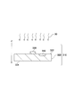
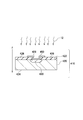
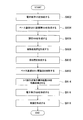
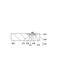
- An example of the section of semiconductor substrate 110 is shown roughly. An example of the section of semiconductor substrate 110 is shown roughly. An example of the section of semiconductor substrate 210 is shown roughly. An example of a section of semiconductor substrate 310 is shown roughly. An example of a section of semiconductor substrate 410 is shown roughly. An example of the section of electronic device 500 is shown roughly. 5 is a flowchart illustrating an example of a method for manufacturing the electronic device 500.
- An example of the section in the manufacture process of semiconductor substrate 510 is shown roughly.
- An example of the section in the manufacture process of semiconductor substrate 510 is shown roughly.
- An example of the semiconductor substrate 910 in the manufacture process of the semiconductor substrate 510 is shown schematically.
- An example of the semiconductor substrate 910 in the manufacture process of the semiconductor substrate 510 is shown schematically.
- An example of the section of semiconductor substrate 510 is shown roughly.
- An example of the section of heat treatment equipment 1200 is shown roughly.
- An example of a section of semiconductor substrate 1310 is shown roughly.
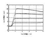
- An example of the semiconductor substrate 910 in the manufacture process of the semiconductor substrate 510 is shown schematically. It is a cross-sectional TEM photograph of the semiconductor substrate 910 taken out from the reaction container. 4 is a cross-sectional TEM photograph of a semiconductor substrate 910 having a Si x Ge 1-x crystal 2000 that has not been heat-treated. The collector current with respect to the collector voltage of HBT is shown.
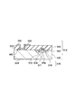
- FIG. 1A schematically shows an example of a cross section of the semiconductor substrate 110.
- the semiconductor substrate 110 is manufactured by heat-treating the base substrate 120.
- the base substrate 120 is provided with a heat-treated portion 130 that is heat-treated by irradiation with the electromagnetic wave 10.
- the base substrate 120 is provided with a heated portion 160 that selectively heats the heated portion 130.
- the heated part 160 may include a heated part 130.
- the heated part 160 of this example includes a heat-treated part 130 and an absorption layer 150.
- the selective heating means that a specific region on the base substrate 120 is given more heat than other regions.
- the heated part 160 absorbs the electromagnetic wave 10 and generates heat.
- the heat-treated portion 130 By selectively heating the heat-treated portion 130 with heat generated by the heated portion 160, only the heat-treated portion 130 is selectively annealed, and the semiconductor substrate 110 in which the average dislocation density in the heat-treated portion 130 is reduced is manufactured. it can.
- the base substrate 120 has a first main surface 122 and a second main surface 124.
- the base substrate 120 is, for example, any one of an Si substrate, an SOI (silicon-on-insulator) substrate, a Ge substrate, a GOI (germanium-on-insulator) substrate, and a GaAs substrate.
- the Si substrate may be a single crystal Si substrate.
- the base substrate 120 may be a resin substrate such as a sapphire substrate, a glass substrate, or a PET film.
- the heat-treated portion 130 is, for example, a semiconductor crystal.
- the heat-treated portion 130 is, for example, a chemical vapor deposition method (sometimes referred to as a CVD method), a metal organic chemical vapor deposition method (sometimes referred to as an MOCVD method), or a molecular beam epitaxy method (referred to as an MBE method). Or an atomic layer growth method (sometimes referred to as an ALD method).
- the heat-treated portion 130 includes, for example, a Si x Ge 1-x crystal formed in contact with the first main surface 122 of the base substrate 120.
- x represents a real number that satisfies 0 ⁇ x ⁇ 1.
- defects such as lattice defects are generated.
- the defect is moved to the inside of the Si x Ge 1-x crystal, the Si x Ge 1-x interface or surface of the crystal or, , And captured by an internal gettering sink or the like of the Si x Ge 1-x crystal.
- a high-quality Si x Ge 1-x crystal having a region in which the density of defects represented by threading dislocations reaching the surface of the Si x Ge 1-x crystal is reduced can be obtained.
- an atmosphere for annealing a mixed atmosphere of hydrogen and an inert gas is preferable.
- pits (holes) may be formed on the surface of the Si x Ge 1-x crystal.
- the annealing atmosphere is a mixed atmosphere of hydrogen and an inert gas
- the hydrogen concentration is preferably 90% or more of the mixed atmosphere, and more preferably 95% or more.
- the pressure for annealing a pressure of about 20 kPa or less can be used.
- the absorption layer 150 is provided on the heat-treated portion 130.
- the absorption layer 150 absorbs the electromagnetic wave 10 and generates heat.
- the absorption layer 150 reduces the average dislocation density of the heat-treated portion 130 by heating the heat-treated portion 130 with the generated heat.
- the absorption layer 150 includes, for example, amorphous silicon, a Group 3-5 compound semiconductor, or a Si x Ge 1-x crystal (0 ⁇ x ⁇ 1).
- the absorbing layer 150 generates heat more efficiently than the heat-treated portion 130 when irradiated with electromagnetic waves. That is, the ratio of the heat generation amount of the absorption layer 150 to the energy amount of the electromagnetic wave 10 to be irradiated is larger than the ratio of the heat generation amount to the energy amount of the electromagnetic wave 10 when the heat treatment part 130 is irradiated with the electromagnetic wave 10.
- the energy of the electromagnetic wave 10 is efficiently converted into heat and the heat-treated portion 130 is heated compared to the case where the heated portion 160 does not have the absorbing layer 150. can do.
- positioned in the vicinity of the absorption layer 150 can be selectively heated, without raising the temperature of the base substrate 120 whole. That is, the heat-treated portion 130 can be selectively heated as compared with the region where the absorption layer 150 of the base substrate 120 is not disposed.
- the absorbing layer 150 is preferably arranged in the order of the absorbing layer 150, the heat-treated portion 130, and the base substrate 120 with respect to the transmission direction Z of the electromagnetic wave 10. Thereby, the energy of the irradiated electromagnetic wave 10 is efficiently used. Further, the heat-treated portion 130, the absorption layer 150, and the base substrate 120 may be arranged in this order with respect to the transmission direction Z of the electromagnetic wave 10. Further, the heat-treated portion 130 and the absorption layer 150 may be disposed adjacent to each other on the first main surface 122. Moreover, the absorption layer 150 may be arrange
- the heat-treated portion 130 may be a part of the base substrate 120.
- the heat-treated portion 130 is at least a part of a Si x Ge 1-x crystal layer (0 ⁇ x ⁇ 1) included in the Ge substrate or the GOI substrate. It is.
- the base substrate 120 may have a heat retaining portion that surrounds at least a part of the heat-treated portion 130.
- the material of the heat retaining part is preferably a material having a low thermal conductivity. Thereby, the energy of the electromagnetic wave 10 irradiated to the to-be-heated part 130 is utilized efficiently.
- the Si x Ge 1-x crystal may be amorphous, and may be polycrystalline or single crystal.
- the heat-treated portion 130 may be a group 3-5 compound semiconductor, Si crystal, or amorphous silicon.
- the heat-treated portion 130 may be a region that becomes an impurity region of a semiconductor device.
- the heat-treated portion 130 is an impurity implantation region into which impurities are introduced by, for example, ion implantation.
- impurities are introduced into at least a part of a region to be an impurity implantation region by ion implantation or the like. Thereafter, the region is heated and annealed, whereby the crystallinity of the region is recovered, and an impurity-implanted region in which impurities are activated is formed.
- the heat-treated portion 130 may be an impurity diffusion region where impurities are diffused by heat treatment.
- an impurity diffusion source is formed in at least a part of a region to be the impurity diffusion region by a coating method, a CVD method, or the like. Thereafter, the region is heated and annealed to form an impurity diffusion region.
- the impurity region is, for example, a well, a source region, or a drain region of a MISFET (metal-insulator-semiconductor field-effect transistor).
- the MISFET may be a MOSFET (metal-oxide-semiconductor field-effect transistor).
- the electromagnetic wave 10 passes through the semiconductor substrate 110 in a direction substantially perpendicular to the first main surface 122 from the first main surface 122 of the semiconductor substrate 110 toward the second main surface 124.
- the transmission direction of the electromagnetic wave 10 is not limited to this.
- the “substantially vertical direction” includes not only a strictly vertical direction but also a direction slightly inclined from the vertical in consideration of manufacturing errors of the substrate and each member.
- the term “transmission direction Z” uses the term “transmission” for the purpose of expressing the direction, and does not actually require that the electromagnetic wave 10 is transmitted.
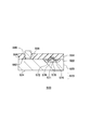
- FIG. 1B schematically shows another example of a cross section of the semiconductor substrate 110.
- the heated portion 160 of this example is different from the configuration of the heated portion 160 shown in FIG. 1A in that the absorbing layer 150 is not included.
- the heat-treated portion 130 and the heated portion 160 indicate the same region.
- the heat-treated part 130 also functions as the absorption layer 150 shown in FIG. 1A.
- the heat-treated portion 130 as the heated portion 160 absorbs the electromagnetic wave 10 and generates heat.
- the heat-treated portion 130 is selectively annealed, and the semiconductor substrate 110 with a reduced average dislocation density can be manufactured.
- the electromagnetic wave 10 has a wavelength at which the absorption coefficient of the heat-treated portion 130 with respect to the electromagnetic wave 10 is larger than the absorption coefficient with respect to the electromagnetic wave 10 of Si contained in the base substrate 120. It is preferable.
- the electromagnetic wave 10 may have a wavelength such that an absorption coefficient in the heat-treated portion 130 is larger than an absorption coefficient in a region other than the heat-treated portion 130 on an electronic device manufactured by dicing the base substrate 120. For example, in the above case, even if the heated portion 160 does not include the absorption layer 150, the heated portion 130 can be selectively heated.
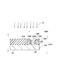
- FIG. 2 schematically shows an example of a cross section of the semiconductor substrate 210.
- the semiconductor substrate 210 includes a base substrate 120, a heat-treated portion 130, and an absorption layer 250.
- the absorption layer 250 is formed in contact with the first major surface 122 of the base substrate 120.
- the heat-treated portion 130 is disposed so that a part of the heat-treated portion 130 is surrounded by the absorption layer 250.
- the absorption layer 250 functions as an inhibition layer that inhibits crystal growth.
- the absorption layer 250 inhibits the precursor of the heat-treated portion 130 from growing into a crystal.
- the absorption layer 250 prevents the compound semiconductor crystal from being epitaxially grown on the surface of the absorption layer 250.
- the absorption layer 250 is, for example, a silicon oxide layer, an aluminum oxide layer, a silicon nitride layer, a silicon oxynitride layer, a tantalum nitride layer or a titanium nitride layer, or a layer in which these are stacked.
- the thickness of the absorption layer 250 is, for example, 0.05 to 5 ⁇ m.
- the absorption layer may be an amorphous silicon layer or a germanium layer.
- the absorption layer 250 can be formed by, for example, a CVD method.
- the opening 256 penetrates the absorption layer 250 to the first main surface 122 in a direction substantially perpendicular to the first main surface 122.
- the opening 256 exposes the first major surface 122.
- the opening 256 is formed by, for example, a photolithography method such as etching.
- a heat-treated portion 130 is formed inside the opening 256.
- a semiconductor such as Si Y Ge 1-Y crystal (0 ⁇ Y ⁇ 1) is formed as the heat-treated portion 130 by the epitaxial growth method, the growth is inhibited on the surface of the absorption layer 250. As a result, the heat-treated portion 130 is selectively grown inside the opening 256.
- the opening 256 has an aspect ratio of, for example, ( ⁇ 3) / 3 or more.
- a crystal having a certain thickness is formed inside the opening 256 having an aspect ratio of ( ⁇ 3) / 3 or more, defects such as lattice defects included in the crystal are terminated on the wall surface of the opening 256. .
- the surface of the crystal exposed in the opening 256 has excellent crystallinity when the crystal is formed.
- the area of the opening 256 may be 1 mm 2 or less, and preferably less than 0.25 mm 2 .
- aspect ratio of opening means a value obtained by dividing “depth of opening” by “width of opening”.
- the aspect ratio is described as (etching depth / pattern width).
- the term of aspect ratio is used with the same meaning.
- the “opening depth” refers to the depth in the stacking direction when a thin film is stacked on the substrate
- the “opening width” refers to the width in the direction perpendicular to the stacking direction.
- the minimum width is used in calculating the aspect ratio of the opening. For example, when the shape of the opening viewed from the stacking direction is a rectangle, the length of the short side of the rectangle is used for calculating the aspect ratio.
- the base substrate 120 is irradiated with the electromagnetic wave 10 in the same manner as when the semiconductor substrate 110 is manufactured.
- the wavelength of the electromagnetic wave 10 is selected so that the electromagnetic wave 10 is absorbed by the absorption layer 250.
- the absorption layer 250 is selectively heated by irradiating the base substrate 120 with the electromagnetic wave 10. it can.
- positioned in the vicinity of the absorption layer 250 can be selectively heated, without raising the temperature of the base substrate 120 whole. That is, the heat-treated portion 130 can be selectively heated as compared with a region of the base substrate 120 where the absorption layer 250 is not disposed.
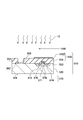
- FIG. 3 schematically shows an example of a cross section of the semiconductor substrate 310.
- the semiconductor substrate 310 includes a base substrate 320, a heat-treated portion 330, and an impurity diffusion region 340.
- the semiconductor substrate 310 is different from the semiconductor substrate 110 and the semiconductor substrate 210 in that it does not include an absorption layer that absorbs the electromagnetic wave 30 and heats the heat-treated portion 330.
- the semiconductor substrate 310 is manufactured by selectively heating the heat-treated portion 330 with the electromagnetic wave 30 while suppressing the impurity diffusion region 340 from being heated.
- the base substrate 320 is an SOI substrate or a Si substrate.
- Base substrate 320 has a first main surface 322 and a second main surface 324.
- Base substrate 320 includes Si crystal on first main surface 322.
- At least a part of the semiconductor device is formed on the first main surface 322 of the base substrate 320.
- an impurity diffusion region 340 of a semiconductor device is formed on the first main surface 322 of the base substrate 320.
- the to-be-heated part 330 and the to-be-heated part 130 shown to FIG. 1A are equivalent.
- the heat-treated portion 330 includes, for example, a Si x Ge 1-x crystal (0 ⁇ X ⁇ 1).
- the heat-treated portion 330 is formed in contact with the first main surface 322 of the base substrate 320, for example. Inside of the Si x Ge 1-x crystal, the difference or the like of the lattice constant between the base substrate 320 and the Si x Ge 1-x crystal, there is a case where defects such as lattice defects are generated.
- the defect is moved to the inside of the Si x Ge 1-x crystal, the Si x Ge 1-x interface or surface of the crystal or, , And captured by an internal gettering sink or the like of the Si x Ge 1-x crystal.
- a high-quality Si x Ge 1-x crystal having a region in which the density of defects represented by threading dislocations reaching the surface of the Si x Ge 1-x crystal is reduced can be obtained.
- the Si x Ge 1-x crystal has a defect trapping portion that traps defects that can move inside the crystal.
- the defect trapping portion is arranged such that the maximum distance from any point included in the Si x Ge 1-x crystal is equal to or less than the distance that the defect can move at the annealing temperature and time.
- the interface of the Si x Ge 1-x crystal, the interface between the sidewall of the opening provided in the inhibition layer and the Si x Ge 1-x crystal, or the internal gettering of the Si x Ge 1-x crystal A sink is an example of a defect capturing unit.
- the Si x Ge 1-x crystal may be formed such that the maximum width does not exceed twice the distance that the defect moves at the annealing temperature and time.
- the impurity diffusion region 340 is formed in at least a part of the base substrate 320.
- the impurity diffusion region 340 is formed in a portion other than the heat-treated portion 330 in the base substrate 320.
- the impurity diffusion region 340 is, for example, a MOSFET well, a source region, or a drain region.
- Impurities contained in the impurity diffusion region 340 diffuse when heated.
- the thermal design of the semiconductor device becomes complicated. Therefore, even when the heat-treated portion 330 is heated, the thermal design can be prevented from becoming complicated by maintaining the temperature of the impurity diffusion region 340 at a temperature lower than the highest temperature of the heat-treated portion 330. .
- the base substrate 320 is irradiated with the electromagnetic wave 30.
- the wavelength of the electromagnetic wave 30 is selected so that the absorption coefficient of the electromagnetic wave 30 into the Si x Ge 1-x crystal is larger than the absorption coefficient of the electromagnetic wave 30 into Si contained in the SOI substrate or Si substrate.
- the electromagnetic wave 30 is, for example, light having a wavelength of 1200 nm to 1800 nm. The light is absorbed by the Si x Ge 1-x crystal (0 ⁇ x ⁇ 1), but is transmitted without being absorbed by the Si crystal.
- the heat-treated portion 330 can be selectively heated.
- the electromagnetic wave 30 is irradiated in the same manner as the electromagnetic wave 10. That is, the heat-treated portion 330 is annealed by the same method as the heat-treated portion 130. Further, the base substrate 320 may be preheated before the electromagnetic wave 30 is irradiated.
- the base substrate 320 may include an active region of an electronic element formed on the base substrate 320.
- the electronic element is, for example, a semiconductor element such as a MOSFET, MISFET, HBT (Heter Junction Bipolar Transistor), HEMT (High Electron Mobility Transistor), a light emitting device such as an LED, a light receiving device such as an optical sensor, or a passive element such as a capacitor.
- the electromagnetic wave 30 is preferably selected so that the absorption coefficient to the heat-treated portion 330 is larger than the absorption coefficient in at least a part of the electronic element.
- the at least part of the region is, for example, an active region of an electronic element.
- At least a part of the semiconductor device formed on the base substrate 320 may include a semiconductor and a dielectric provided in contact with each other.
- the interface between the semiconductor and the dielectric is used as, for example, a MOS gate interface formed in the active region of the MOSFET.
- the MOS gate interface has low heat resistance. Therefore, when the interface is exposed to high temperature conditions for a long time, the characteristics of the MOSFET may deteriorate.
- the interface becomes hot. It can suppress long-term exposure to conditions.
- the wavelength of the electromagnetic wave 30 may be selected such that the absorption coefficient to the heat-treated portion 330 is larger than the absorption coefficient to the semiconductor and the dielectric.
- FIG. 4 schematically shows an example of a cross section of the semiconductor substrate 410.
- the semiconductor substrate 410 is manufactured by irradiating the base substrate 420 with the electromagnetic wave 12.
- the base substrate 420 includes a protective layer 426, a region 430 into which an impurity is introduced, and an absorption layer 450.
- the base substrate 420 has a first main surface 422 and a second main surface 424.
- the base substrate 420, the first main surface 422, and the second main surface 424 of the semiconductor substrate 410 and the base substrate 120, the first main surface 122, and the second main surface 124 of the semiconductor substrate 110 are equivalent.
- the region 430 is an example of the heat-treated portion 130.
- an impurity is introduced into the region 430 by an ion implantation method.
- the absorption layer 450 is provided above the region 430.
- the protective layer 426 protects the region other than the region to be heated in the base substrate 420 from the electromagnetic wave 12.
- An opening 428 is formed in the protective layer 426.
- “above A” includes the surface of “A” on a line extending from “A” in the direction toward the irradiation source of the electromagnetic wave 12 irradiated to the heat-treated portion 130.
- Arbitrary position. “A” is, for example, the base substrate 120 and the heat-treated portion 130. That is, “above A” may refer to “A” and an arbitrary position between the irradiation sources that irradiate the electromagnetic wave 12.
- the absorption layer 450 is provided so that the region 430 is sandwiched between the absorption layer 450 and the base substrate 420.
- “above the region 430” corresponds to the side opposite to the base substrate 420 with respect to the interface between the region 430 and the absorption layer 450.
- Below A refers to an arbitrary position on a line extending from “A” in the direction opposite to the direction toward the irradiation source of the electromagnetic wave irradiated to the heat-treated portion 130. That is, “below A” may refer to an arbitrary position on the opposite side of “above A” starting from “A”.
- the semiconductor substrate 410 is manufactured by selectively heating the absorption layer 450 by irradiating the base substrate 420 with the electromagnetic wave 12.
- the protective layer 426 prevents the region other than the region 430 from being heated by the electromagnetic wave 12.
- the maximum temperature reached in the region other than the region 430 can be maintained at a temperature lower than the maximum temperature reached in the region 430.
- the region 430 covered with the absorption layer 450 can be selectively heated.
- the impurity region can be activated.
- the protective layer 426 shields at least a part of the electromagnetic wave 12 and weakens the strength of the electromagnetic wave 12 after passing through the protective layer 426. Thereby, the area
- the protective layer 426 may include a reflective layer that reflects at least a part of the electromagnetic wave 12.
- the reflective layer is a metal thin film such as Ag, Au, or Al.
- the protective layer 426 may have a scattering layer that scatters at least a part of the electromagnetic wave 12.
- the scattering layer is, for example, a resin layer containing fine particles, or a layer in which fine particles are dispersed in dielectrics having different refractive indexes.
- the fine particles may be transparent fine particles, and examples thereof include ceramic fine particles such as colloidal silica.
- the scattering layer is formed by, for example, a coating method.
- the scattering layer scatters at least a part of the electromagnetic wave 10 incident on the inside of the protective layer 426 to change the traveling direction of the electromagnetic wave 12. Thereby, the moving distance of the electromagnetic wave 12 inside the protective layer 426 is increased, and the electromagnetic wave 12 is prevented from reaching the region to be protected from the electromagnetic wave 12.
- the protective layer 426 is composed of a plurality of materials.
- a reflector such as a metal thin film and a scatterer such as a fine particle are embedded in, for example, a silicon oxide layer, a silicon nitride layer, a silicon oxynitride layer, an aluminum oxide layer, or a layer in which these layers are stacked. Be placed.
- the protective layer 426 may have a thermal diffusion layer that diffuses heat generated by the irradiation of the electromagnetic wave 12. Thereby, the protective layer 426 protects a region existing in the heat transfer direction of the heat generated by the irradiation of the electromagnetic wave 12.
- the thermal diffusion layer is, for example, a silicon oxide layer, a silicon nitride layer, a silicon oxynitride layer, an aluminum oxide layer, or a layer in which these are stacked.
- the thermal diffusion layer may be formed from a plurality of layers. Thereby, since conduction of thermal energy is suppressed by the contact thermal resistance between the layers, the amount of heat reaching the region to be protected from the electromagnetic wave 12 can be further reduced.
- the protective layer 426 is disposed in the order of the protective layer 426 and the base substrate 420 with respect to the transmission direction of the electromagnetic wave 12.
- the protective layer 426 may be formed in contact with the first main surface 422 of the base substrate 420.
- the protective layer 426 is formed so as to entirely cover the base substrate 420, but the protective layer 426 may be formed so as to protect at least a part of the portion other than the region 430.
- the protective layer 426 is formed above a region with low heat resistance disposed on the semiconductor substrate 410.
- the opening 428 penetrates the protective layer 426 to the first main surface 422 in a direction substantially perpendicular to the first main surface 422. Opening 428 exposes at least a portion of region 430.
- the region since the region other than the opening 428 of the base substrate 420 is covered with the protective layer 426, the region is protected from the electromagnetic wave 12 or the heat generated by the irradiation of the electromagnetic wave 12.
- the size of the impurity region can be adjusted. That is, not all of the region 430 is exposed from the opening 428, but a part of the region 430 may be exposed from the opening 428.
- the opening 428 can be formed by, for example, a photolithography method such as etching.
- the absorption layer 450 is the same as the absorption layer 150 and the absorption layer 250 except that at least a part is formed inside the opening 428.
- the absorption layer 450 is preferably formed in contact with at least part of the region 430 inside the opening 428. Thereby, the absorption layer 450 can heat the region 430 by the heat generated by absorbing the electromagnetic wave 12. As a result, the absorption layer 450 can selectively heat the region 430.
- the base substrate 420 is irradiated with the electromagnetic wave 12 in the same manner as when the semiconductor substrate 110 is manufactured.
- the wavelength of the electromagnetic wave 12 is selected such that the absorption coefficient of the electromagnetic wave 12 in the absorption layer 450 is larger than the absorption coefficient in the region 430 of the electromagnetic wave 12.
- the wavelength of the electromagnetic wave 12 is selected so that at least a part of the electromagnetic wave 12 is shielded by the protective layer 426.
- the electromagnetic wave 12 is equivalent to the electromagnetic wave 10 except for the selected wavelength.
- the semiconductor substrate 410 is irradiated with the electromagnetic wave 12 to selectively heat the absorption layer 450, Region 430 can be selectively heated.
- the temperature of the region protected by the protective layer 426 can be maintained at a temperature lower than the highest temperature reached in the region 430.
- the impurity region is activated by selectively annealing the region 430 into which the impurity is introduced.
- the annealing of the region 430 can be performed under the same conditions as the annealing of the heat-treated portion 130.
- the semiconductor substrate 410 may be preheated before the electromagnetic wave 12 is irradiated.
- FIG. 5 schematically shows an example of a cross section of the electronic device 500.
- the electronic device 500 includes a semiconductor substrate 510, a second electronic element 580, a wiring 592, a wiring 594, and a wiring 596.
- the semiconductor substrate 510 includes a base substrate 520, an inhibition layer 554, a Si x Ge 1-x crystal 562, and a group 3-5 compound semiconductor 566.
- the base substrate 520 has a first main surface 522 and a second main surface 524.
- a first electronic element 570 is formed on the base substrate 520.
- the first electronic element 570 includes a well 571, a source region 572, a drain region 574, a gate electrode 576, and a gate insulating film 578.
- an opening 556, an opening 593, and an opening 595 are formed.
- the second electronic element 580 includes an input / output electrode 587, an input / output electrode 588, and a gate electrode 589.
- the second electronic element 580 is formed in the group 3-5 compound semiconductor 566.
- the inhibition layer 554 protects the first electronic element 570 from electromagnetic waves.
- the semiconductor substrate 510 is manufactured by selectively heating the Si x Ge 1-x crystal 562 by irradiating the base substrate 520 with an electromagnetic wave that is hardly absorbed by the inhibition layer 554.
- the inhibition layer 554 may function as a heat conduction suppression layer that suppresses heat generated by receiving electromagnetic waves from being transmitted to the first electronic element 570.
- the inhibition layer 554 inhibits the precursors of the Si x Ge 1-x crystal 562 and the group 3-5 compound semiconductor 566 from growing into a crystal.
- the inhibition layer 554 inhibits the crystal of the Group 3-5 compound semiconductor 566 from growing epitaxially on the surface of the inhibition layer 554.
- the inhibition layer 554 is, for example, a silicon oxide layer, an aluminum oxide layer, a silicon nitride layer, a silicon oxynitride layer, a tantalum nitride layer, a titanium nitride layer, or a layer in which these are stacked.
- the thickness of the inhibition layer 554 is, for example, 0.05 to 5 ⁇ m.
- the inhibition layer 554 is formed in contact with the first major surface 522 of the base substrate 520.
- the inhibition layer 554 can be formed by, for example, a CVD method.
- the opening 556 penetrates the inhibition layer 554 to the first main surface 522 in a direction substantially perpendicular to the first main surface 522.
- the opening 556 exposes the first main surface 522. Thereby, a crystal can be selectively grown inside the opening 556.
- the opening 556 can be formed by etching, for example.
- the openings 593 and 595 penetrate the inhibition layer 554 in a direction substantially perpendicular to the first main surface 522. Opening 593 and opening 595 expose source region 572 and drain region 574, respectively. A part of the wiring 592 and part of the wiring 594 are formed in the opening 593 and the opening 595, respectively. Thereby, the first electronic element 570 is electrically coupled to another electronic element such as the second electronic element 580.
- the opening 593 and the opening 595 can be formed by, for example, reactive ion etching.
- the Si x Ge 1-x crystal 562 is an example of a seed crystal that provides a good seed surface for growing the Group 3-5 compound semiconductor 566.
- x represents a real number that satisfies 0 ⁇ x ⁇ 1.
- the Si x Ge 1-x crystal 562 suppresses impurities existing in the base substrate 520 or the first main surface 522 from adversely affecting the crystallinity of the group 3-5 compound semiconductor 566.
- the Si x Ge 1-x crystal 562 is provided inside the opening 556.
- the Si x Ge 1-x crystal 562 is formed in contact with the first major surface 522, for example.
- the Si x Ge 1-x crystal 562 can be formed by, for example, an epitaxial growth method such as a CVD method. At this time, since the precursors of the Si x Ge 1-x crystal 562 at the surface of the inhibition layer 554 is inhibited to grow the crystal, Si x Ge 1-x crystal 562 is selectively grown within the openings 556 . Thereby, the Si x Ge 1-x crystal 562 can be locally formed.
- the Si x Ge 1-x crystal 562 is preferably annealed. The annealing of the Si x Ge 1-x crystal 562 can be performed under the same conditions as the annealing of the heat-treated portion 130. Thereby, in the Si x Ge 1-x crystal 562, the internal defect density mainly including threading dislocations reaching the surface can be reduced, and a good seed surface can be provided for the Group 3-5 compound semiconductor 566.
- the substrate is irradiated with electromagnetic waves that can be absorbed by the absorption layer, The Si x Ge 1-x crystal 562 is heated.
- the ratio of the heat generation amount with respect to the electromagnetic wave energy amount in the absorption layer is preferably larger than the ratio of the heat generation amount with respect to the electromagnetic wave energy amount when at least a part of the first electronic element 570 or the inhibition layer 554 is irradiated with the electromagnetic wave. .
- the absorption coefficient of the electromagnetic wave in the Si x Ge 1-x crystal 562 is close to the absorption coefficient of the electromagnetic wave in the inhibition layer 554 or the first electronic element 570. Even in such a case, the Si x Ge 1-x crystal 562 can be selectively heated with respect to the inhibition layer 554 or the first electronic element 570.
- the Group 3-5 compound semiconductor 566 is lattice-matched or pseudo-lattice-matched to the Si x Ge 1-x crystal 562.
- the Group 3-5 compound semiconductor 566 is GaAs or the like.
- the Group 3-5 compound semiconductor 566 is formed in contact with the Si x Ge 1-x crystal 562.
- X is 0.1 or less, the difference in lattice constant between the Si x Ge 1-x crystal 562 and the group 3-5 compound semiconductor 566 becomes smaller, and defects are less likely to occur.
- “pseudo-lattice matching” is not perfect lattice matching, but the difference between the lattice constants of two semiconductors is small, and the occurrence of defects due to lattice mismatch is not significant.
- the interface between the Si x Ge 1-x crystal 562 and the group 3-5 compound semiconductor 566 may be inside the opening 556.
- the Group 3-5 compound semiconductor 566 can be formed by an epitaxial growth method such as an MOCVD method, for example.
- the base substrate 520 is a substrate having a Si x Ge 1-x crystal (0 ⁇ x ⁇ 1) on the first main surface 522, such as a Ge substrate and a GOI substrate
- a Group 3-5 compound The semiconductor 566 may be formed in contact with the first major surface 522 using the Si x Ge 1-x crystal (0 ⁇ x ⁇ 1) as a seed crystal.
- the group 3-5 compound semiconductor 566 When the group 3-5 compound semiconductor 566 is epitaxially grown by MOCVD, the above-described absorption layer that absorbs electromagnetic waves and generates heat to heat the Si x Ge 1-x crystal 562 is formed on the substrate.
- the source gas may be supplied to the reaction vessel while irradiating the base substrate 520 with electromagnetic waves that can be absorbed by the absorption layer.
- a group 3-5 compound semiconductor lattice-matched or pseudo-lattice-matched to the Si x Ge 1-x crystal can be selectively formed on the surface of the annealed Si x Ge 1-x crystal 562.
- the temperature of the base substrate 520 in particular, the temperature of the region where the first electronic element 570 is formed is maintained at 650 ° C. or lower, preferably 450 ° C. or lower. Thereby, it can suppress that the 1st electronic element 570 deteriorates with a heat
- the temperature of the base substrate 520 is 650 ° C. or lower, preferably when the Si x Ge 1-x crystal 562 is formed on the base substrate 520 and when the Si x Ge 1-x crystal 562 is annealed. It is maintained at 450 ° C. or lower.
- a growth pressure of 0.1 kPa or more and 100 kPa or less can be used. If the growth pressure is high, crystals are likely to be formed on the inhibition layer, which is not preferable. A preferable growth pressure is 50 kPa or less.
- the growth rate of the Group 3-5 compound semiconductor 566 depends on the area ratio of the opening 556 provided in the inhibition layer 554 ((bottom area of the opening) / (area of the surface where the inhibition layer and the substrate are in contact)). When the area ratio of the opening 556 is reduced, a large amount of raw material is concentrated on the opening, and the growth rate is increased.
- the first electronic element 570 may be formed in a region other than the region exposed to the opening 556 of the base substrate 520.
- a MOSFET is exemplified as the first electronic element 570, but the first electronic element 570 may be an element other than the MOSFET.
- the first electronic element 570 includes, for example, a driving circuit for the second electronic element 580, a correction circuit that improves linearity in input / output characteristics of the second electronic element 580, and an input stage of the second electronic element 580. At least one of the protection circuits.
- the first electronic element 570 is included in a semiconductor device such as MISFET, HBT, and HEMT, a light emitting device such as a semiconductor laser, a light emitting diode, and a light emitting thyristor, a light receiving device such as an optical sensor, a light receiving diode, and a device such as a solar cell. It may be an active element.
- the first electronic element 570 may be a passive element such as a resistor, a capacitor, and an inductor.
- HBT is exemplified as the second electronic element 580
- the second electronic element 580 is an electronic device of at least one of an analog electronic device, a light emitting device such as an LED, and a light receiving device such as an optical sensor. You may have an element.
- the second electronic element 580 is a semiconductor device such as a MOSFET, MISFET, HBT, or HEMT, a light emitting device such as a semiconductor laser, a light emitting diode, or a light emitting thyristor, a light receiving device such as a light sensor, a light receiving diode, or an active device included in a solar cell. It may be an element.
- the first electronic element 570 may be a passive element included in a resistor, a capacitor, an inductor, and the like.
- the material of the input / output electrode 587, the input / output electrode 588, and the gate electrode 589 is, for example, a conductive material, and is a metal such as Al, W, Ti, or a semiconductor doped with impurities at a high concentration.
- the input / output electrode 587, the input / output electrode 588, and the gate electrode 589 can be formed by, for example, a vacuum deposition method or a plating method.
- the wiring 592, the wiring 594, and the wiring 596 electrically couple the first electronic element 570 or the first electronic element 570 with another electronic element or the like.
- the material of the wiring 592, the wiring 594, and the wiring 596 may be a conductive material.
- a metal such as Al, Cu, Au, W, or Ti, or a semiconductor doped with impurities can be used.
- the wiring 592, the wiring 594, and the wiring 596 can be formed by, for example, a vacuum evaporation method or a plating method.
- the semiconductor substrate 510 may include a plurality of first electronic elements 570.
- One first electronic element 570 may be electrically coupled to a plurality of second electronic elements 580.
- the semiconductor substrate 510 may include a plurality of second electronic elements 580.
- One second electronic element 580 may be electrically coupled to a plurality of first electronic elements 570.
- FIG. 6 is a flowchart showing an example of a method for manufacturing the electronic device 500.
- the first electronic element 570 is formed on the base substrate 520.
- at least the inhibition layer 554 that inhibits the precursor of the Si x Ge 1-x crystal 562 from growing into the crystal and protects the first electronic element 570 from the electromagnetic wave 10 is provided at least in the first step.
- 1 electronic element 570 is formed so as to cover.
- step S ⁇ b> 606 an opening 556 that penetrates to the base substrate 520 is formed in the region of the inhibition layer 554 other than the region that covers the first electronic element 570.
- a Si x Ge 1-x crystal 562 is provided in the opening 556 as a heat-treated portion. That is, a precursor of the Si x Ge 1-x crystal 562 is grown into a crystal in the opening 556.
- an absorption layer that absorbs the electromagnetic wave 10 and selectively heats the Si x Ge 1-x crystal 562 is provided.
- the Si x Ge 1-x crystal 562 is annealed by heat generated by the absorption layer by irradiating the base substrate with electromagnetic waves while heating the base substrate as a whole.
- step S614 a Group 3-5 compound semiconductor 566 is grown on the Si x Ge 1-x crystal 562.
- step S616 the second electronic element 580 is formed in the group 3-5 compound semiconductor 566.
- step S618, the opening 593 and the opening 595 are formed in the inhibition layer 554. Further, the wiring 592, the wiring 594, and the wiring 596 are formed, whereby the electronic device 500 is obtained.
- FIG. 7 schematically shows an example of a cross section in the process of manufacturing the semiconductor substrate 510.
- the first electronic element 570 is formed on the base substrate 520.
- the base substrate 520 is, for example, a Si substrate or an SOI substrate.
- FIG. 8 schematically shows an example of a cross section in the process of manufacturing the semiconductor substrate 510.
- the inhibition layer 554 is formed in contact with the first main surface 522 of the base substrate 520.
- Inhibition layer 554 is, for example, SiO 2.
- the thickness of the inhibition layer 554 is, for example, 0.05 to 5 ⁇ m.
- the inhibition layer 554 may be formed by a CVD method.
- An opening 556 is formed in the inhibition layer 554 by, for example, a photolithography method such as etching.
- the opening 556 may have an aspect ratio of ( ⁇ 3) / 3 or more.
- FIG. 9 schematically shows an example of the semiconductor substrate 910 in the process of manufacturing the semiconductor substrate 510.
- an Si x Ge 1-x crystal 962 which is an example of a heat-treated portion, is provided in the opening 556 by an epitaxial growth method.
- the Si x Ge 1-x crystal 962 corresponds to the heat-treated portion 130 described with reference to FIGS. 1A to 2.
- the step of reducing the lattice defect density by irradiating an electromagnetic wave to Si x Ge 1-x crystal 962 reduces the lattice defect density of the Si x Ge 1-x crystal 962.
- An absorption layer 950 is formed on the Si x Ge 1-x crystal 962 before irradiating the Si x Ge 1-x crystal 962 with electromagnetic waves.
- the absorption layer 950 may be formed at least partially inside the opening 556.
- the absorption layer 950 may be formed in contact with at least a part of the Si x Ge 1-x crystal 962.
- the absorption layer 950 is, for example, amorphous silicon.
- the absorption layer 950 can be formed by, for example, a CVD method.
- the Si x Ge 1-x crystal 962 is provided by, for example, a CVD method in which a part of the source gas contains halogen. Since the precursor of the Si x Ge 1-x crystal 962 is inhibited from growing on the surface of the inhibition layer 554, the Si x Ge 1-x crystal 962 is selectively grown inside the opening 556. At this time, defects such as lattice defects may occur inside the Si x Ge 1-x crystal 962.
- the defect density inside the Si x Ge 1-x crystal 562 can be reduced.
- the first electronic element 570 may be damaged if high-temperature annealing at 800 to 900 ° C. is performed. Further, impurities contained in the well 571, the source region 572, and the drain region 574 are further diffused.
- the inhibition layer 554 protects the first electronic element 570 from electromagnetic waves, whereby damage to the first electronic element 570 can be prevented.
- the wavelength of the electromagnetic waves is preferably selected so that the absorption coefficient of the electromagnetic waves in the inhibition layer 554 and the first electronic element 570 becomes small.
- the Si x Ge 1-x absorption coefficient of the electromagnetic wave decreases in the crystal 962, can not heat the Si x Ge 1-x crystal 962 efficiently.
- the ratio of the calorific value with respect to the amount of energy of the irradiated electromagnetic wave is larger than the ratio of the calorific value with respect to the amount of electromagnetic wave energy when the Si x Ge 1-x crystal 962 is irradiated with the electromagnetic wave.
- the Si x Ge 1-x crystal 962 can be selectively heated.
- the absorption layer 950 is preferably formed at a position closer to the Si x Ge 1-x crystal 962 than to the first electronic element 570.
- the Si x Ge 1-x is not damaged without damaging the first electronic element 570.
- Crystal 962 can be selectively heated.
- the absorption layer 950 preferably has a ratio of the heat generation amount with respect to the energy amount of the irradiated electromagnetic wave larger than a ratio of the heat generation amount with respect to the energy amount of the electromagnetic wave when the first electronic element 570 is irradiated with the same electromagnetic wave. Thereby, the Si x Ge 1-x crystal 962 can be selectively heated without damaging the first electronic element 570.
- the semiconductor substrate 910 may be preheated before the step of selectively heating the Si x Ge 1-x crystal 962.
- the preheating for example, a support body heated to a constant temperature is brought into contact with the second main surface 524 of the base substrate 520, and the semiconductor substrate 910 is entirely heated by heat conduction from the support body to the semiconductor substrate 910. , By heating the Si x Ge 1-x crystal 962 and the first electronic element 570.
- the semiconductor substrate 910 may be entirely heated by irradiating the base substrate 520 with electromagnetic waves absorbed by the base substrate 520 from the second main surface 524 side of the base substrate 520. Further, the preheating is performed so that the temperature of the first electronic element 570 does not exceed the temperature at which the first electronic element 570 is thermally deteriorated.
- FIG. 10 schematically shows an example of the semiconductor substrate 910 in the manufacturing process of the semiconductor substrate 510.
- the electromagnetic wave 14 is irradiated from above the base substrate 520.
- the electromagnetic wave 14 may be continuous light or may be flash light of a flash lamp.
- the electromagnetic wave 14 is equivalent to the electromagnetic wave 10 except for the selected wavelength.
- the wavelength of the electromagnetic wave 14 is selected so that the absorption coefficient of the electromagnetic wave 14 in the inhibition layer 554 and the first electronic element 570 is smaller than the absorption coefficient of the electromagnetic wave 14 in the absorption layer 950. Further, the electromagnetic wave 14 is absorbed by the absorption layer 950, and the absorption layer 950 is selectively heated. Due to heat transfer from the absorption layer 950, the Si x Ge 1-x crystal 962 is heated, and the Si x Ge 1-x crystal 962 is annealed. The annealing can be performed under the same conditions as the annealing of the heat-treated portion 130. At this time, since the first electronic element 570 is difficult to absorb the electromagnetic wave 14, the temperature increase of the first electronic element 570 is suppressed.
- the average dislocation density of threading dislocations penetrating to the surface of the Si x Ge 1-x crystal 562 is, for example, 10 5 cm ⁇ 2 or less. That is, in the step of reducing the lattice defect density of the Si x Ge 1-x crystal 562 reduces, by irradiation of an electromagnetic wave 14, the average dislocation density in the interior of the Si x Ge 1-x crystal 562 to 10 5 cm -2 or less it can.
- the average dislocation density can be measured by plane cross-sectional observation using an etch pit method or a transmission electron microscope.
- the absorption layer 950 may be removed by etching or the like.
- the steps of reducing the lattice defect density of SixGe 1-x crystal 962 described in connection with FIG. 10 May be performed within the same reaction vessel. Further, after the step of growing the precursors of the Si x Ge 1-x crystal 962 crystal without Si x Ge 1-x crystal 962 is exposed to the atmosphere, continuously, Si x Ge 1-x crystal 962 The step of reducing the lattice defect density may be performed.
- FIG. 11 schematically shows an example of a cross section of the semiconductor substrate 510.
- the absorption layer 950 shown in FIG. 10 is removed by etching or the like.
- a Group 3-5 compound semiconductor 566 is formed on the Si x Ge 1-x crystal 962 having a reduced average dislocation density.
- the Group 3-5 compound semiconductor 566 is preferably lattice-matched or pseudo-lattice-matched to the Si x Ge 1-x crystal 562.
- the Group 3-5 compound semiconductor 566 is epitaxially grown using the surface of the Si x Ge 1-x crystal 562 having excellent crystallinity as a seed surface.
- the Group 3-5 compound semiconductor 566 can be formed by, for example, the MOCVD method. After that, the second electronic element 580, the wiring 592, the wiring 594, the wiring 596, and the like are formed, and the first electronic element 570 and the second electronic element 580 are electrically coupled to obtain the electronic device 500. .
- the same electromagnetic wave is again applied to the base substrate 520 using the light source irradiated with the electromagnetic wave in the stage of reducing the lattice defect density of the Si x Ge 1-x crystal 562. May be irradiated.
- the absorption layer 950 shown in FIG. 10 is removed, but a part of the absorption layer 950 may be left.
- the group 3-5 compound semiconductor 566 and the base substrate 520 can be insulated by leaving a part of the absorption layer 950.
- the insulator precursor may be a Group 3-5 compound semiconductor that is oxidized to become an insulator.
- the insulator precursor is a Group 3-5 compound semiconductor containing Al or B.
- the insulator is an oxide dielectric obtained by oxidizing a precursor of an insulator including a Group 3-5 compound semiconductor containing Al, for example.
- the insulator and the insulator precursor may be lattice-matched or pseudo-lattice-matched with the Si x Ge 1-x crystal 562.
- the group 3-5 compound semiconductor 566 may be grown with the absorption layer formed on the semiconductor substrate 910. Accordingly, the Group 3-5 compound semiconductor 566 that lattice-matches or pseudo-lattice-matches to the Si x Ge 1-x crystal 562 can be formed while suppressing the temperature rise of the first electronic element 570. For example, while the absorption layer is formed in a position closer to the Si x Ge 1-x crystal 562 than the first electronic element 570 inside the inhibition layer 554, while irradiating the substrate with electromagnetic waves that can be absorbed by the absorption layer, Feed the raw material gas into the reaction vessel. Thus, a group 3-5 compound semiconductor that lattice matches or pseudo-lattice matches with the Si x Ge 1-x crystal 562 can be selectively formed on the surface of the annealed Si x Ge 1-x crystal 562.
- the temperature of the base substrate 520 in particular, the temperature of the region where the first electronic element 570 is formed is preferably maintained at 650 ° C. or lower, preferably 450 ° C. or lower. Thereby, it can suppress more that the 1st electronic element 570 deteriorates with a heat
- the base substrate is also formed while the Si x Ge 1-x crystal 562 is formed on the base substrate 520, while the semiconductor substrate 910 is preheated, and during the annealing of the Si x Ge 1-x crystal 562.
- the temperature of 520 is preferably maintained at 650 ° C. or lower, preferably 450 ° C. or lower.
- the wavelength of the electromagnetic wave 14 is selected so that the absorption coefficient of the electromagnetic wave 14 in the inhibition layer 554 and the first electronic element 570 is smaller than the absorption coefficient of the electromagnetic wave 14 in the absorption layer 950.
- the method of manufacturing the electronic device 500 is not limited to this.
- As the base substrate 520 an SOI substrate or a base substrate containing Si, such as an Si substrate, is prepared, and the absorption coefficient of the Si x Ge 1-x crystal in the Si x Ge 1-x crystal 562 is changed to an SOI substrate or Si substrate.
- the Si x Ge 1-x crystal 562 may be selectively heated by irradiating an electromagnetic wave larger than the absorption coefficient of Si contained in the substrate. In this case, the absorption layer 950 may not be formed.
- FIG. 12 schematically shows an example of a cross section of the heat treatment apparatus 1200.
- FIG. 12 shows the heat treatment apparatus 1200 together with the base substrate 1280 disposed inside the heat treatment apparatus 1200.
- the heat treatment apparatus 1200 is an example of a reaction apparatus.
- the base substrate 1280 has the same configuration as any of the base substrate 120, the base substrate 320, the base substrate 420, and the base substrate 520, for example.
- On the first main surface 1282 of the base substrate 1280 as an example, a heat-treated portion 130 to be heat-treated and an absorption layer 150 are provided.
- the heat treatment apparatus 1200 is an example of a reaction apparatus.
- the heat treatment apparatus 1200 performs heat treatment such as flash annealing on the base substrate 1280.
- the heat treatment apparatus 1200 may also serve as a CVD apparatus for forming a Si crystal, a Si x Ge 1-x crystal (0 ⁇ x ⁇ 1), a compound semiconductor crystal, and the like on the base substrate 1280.
- the heat treatment apparatus 1200 includes a heat treatment furnace 1210, a lamp unit 1230 and a lamp unit 1240, a radiation thermometer 1252, and a control unit 1260.
- the heat treatment furnace 1210 includes a wafer carry-in port 1212, a gas inflow portion 1214, a gas discharge portion 1216, and a lid portion 1222.
- the lamp unit 1230 includes a lamp 1232, a reflecting member 1234, a filter 1236, and a power supply unit 1238.
- the lamp unit 1240 includes a lamp 1242, a reflecting member 1244, and a power supply unit 1248.
- the heat treatment furnace 1210 accommodates the base substrate 1280 therein.
- the heat treatment furnace 1210 is an example of a reaction vessel.
- the heat treatment furnace 1210 has, for example, a hollow cylindrical shape.
- the wafer carry-in port 1212 is used for carrying in or taking out the base substrate 1280.
- the lid 1222 seals the wafer carry-in port 1212.
- the lid 1222 may include a support 1224 that supports the base substrate 1280 inside the heat treatment apparatus 1200. Thus, the heat treatment furnace 1210 can hold the base substrate 1280 inside.
- the support 1224 is, for example, a susceptor made of graphite.
- a temperature sensor as a heating temperature measurement unit that measures the temperature of the support 1224 may be disposed on the support 1224.
- the base substrate 1280 may be placed in contact with the support 1224. In this case, the lower temperatures of the support 1224 and the base substrate 1280 are substantially the same. Therefore, the temperature sensor can measure the temperature of the back surface of the base substrate 1280.
- the temperature sensor can measure the temperature of a portion having a small heat resistance formed on the base substrate 1280.
- the temperature sensor may measure the temperature in the vicinity of the Si device or the Group 3-5 compound semiconductor device formed on the base substrate 1280.
- an inert gas or the like is supplied from the gas inflow portion 1214 into the heat treatment furnace 1210. Further, the gas inside the heat treatment furnace 1210 may be discharged from the gas discharge unit 1216.
- the gas inflow portion 1214 supplies a source gas such as CVD or MOCVD into the heat treatment furnace 1210.
- the gas inflow portion 1214 supplies the source gas 1290 and the carrier gas into the heat treatment furnace 1210.
- the carrier gas is, for example, hydrogen gas.
- the reaction of the source gas 1290 causes a semiconductor crystal to grow epitaxially on the base substrate 1280 held in the heat treatment furnace 1210.
- Residual gas or the like in the reaction vessel is discharged from the gas discharge unit 1216.
- the gas discharge unit 1216 may be connected to a vacuum system.
- the temperature of the source gas 1290 is lower than the temperature of the base substrate 1280.
- the base substrate 1280 is preferably cooled by the source gas 1290 while the base substrate 1280 is irradiated with electromagnetic waves to epitaxially grow a semiconductor crystal.
- the heat-treated portion 130 can be selectively heated while maintaining a temperature difference in a region other than the heat-treated portion 130 of the base substrate 1280.
- the lamp unit 1230 is an example of an irradiation unit.
- the lamp unit 1230 is disposed on the first main surface 1282 side of the base substrate 1280.
- the lamp unit 1230 irradiates the base substrate 1280 with electromagnetic waves from the first main surface 1282 side of the base substrate 1280. As a result, the lamp unit 1230 heats the base substrate 1280.
- Each lamp 1232 generates an electromagnetic wave.
- the lamp 1232 generates light including, for example, infrared rays.
- Each lamp 1232 may generate incoherent light that uniformly radiates electromagnetic waves to the entire base substrate 1280.
- the heat treatment apparatus 1200 can heat-treat the base substrate 120 having a large area at once by, for example, arranging a plurality of inexpensive light sources in parallel and irradiating the entire base substrate 120 with electromagnetic waves uniformly.
- the lamp 1232 is, for example, a high-intensity discharge lamp, a halogen lamp, a xenon lamp, or an LED lamp.
- the high-intensity discharge lamp is, for example, a high-pressure mercury lamp, a metal halide lamp, or a sodium lamp.
- the lamp unit 1230 may continuously irradiate electromagnetic waves, or may irradiate electromagnetic waves a plurality of times in a pulsed manner.
- the lamp unit 1230 may determine the time and number of times to irradiate the electromagnetic wave in a pulsed manner according to the application of irradiating the electromagnetic wave.
- the lamp unit 1230 performs flash annealing by irradiating the base substrate 1280 with an electromagnetic wave a plurality of times in a pulsed manner.
- the lamp unit 1230 irradiates the base substrate 1280 with flash light using a flash lamp such as a xenon lamp.
- the surface layer portion of the base substrate 1280 is heated to a high temperature of, for example, 1000 ° C. or more in a short time.
- the entire surface of the base substrate 1280 is heated by irradiating the base substrate 1280 with flash light from a flash lamp while scanning the base substrate 1280.
- the pulse width of the electromagnetic wave irradiated by the flash lamp is, for example, 1 ns to 100 ms. In the case where the base substrate 1280 is heat-treated at a high temperature, it is preferable that the pulse width of the electromagnetic wave be short. However, when the pulse width is smaller than 0.1 ms, it becomes difficult to control the optical pulse. Therefore, the pulse width of the electromagnetic wave is preferably 0.1 ms to 10 ms.
- the pulse width means a time width in which the level of the pulse waveform maintains a magnitude of 1/2 or more of the peak value.
- the light irradiation amount of the flash light can be arbitrarily selected depending on the heat treatment target and the available lamp.
- the light irradiation amount is, for example, 2 to 50 J / cm 2 .
- the light irradiation amount of the flash lamp means the energy (unit: J) of electromagnetic waves output from the flash lamp, and the area (unit: cm 2 ) of the region irradiated with the flash lamp in the base substrate 1280. The value divided by.
- the pulse interval of the flash light is set in consideration of the output performance and repeated charge / discharge performance of the flash light source and the heat dissipation of the heat-treated portion 130.
- the temperature of the heat-treated portion 130 reaches a necessary annealing temperature, and the temperature of the base substrate 1280 other than the heat-treated portion 130 is set not to exceed a predetermined temperature.
- the pulse interval is, for example, 1 s or longer.
- the number of times the flash lamp is turned on and the pulse width of each pulse may be freely set so that the heat-treated portion 130 receives a sufficient annealing effect.
- the temperature and time of the heat treatment can be adjusted by adjusting the number of pulses of the flash lamp or the pulse width of each pulse.
- the temperature and time of the heat treatment are as follows. 850 to 900 ° C. for 2 to 10 minutes.
- the annealing temperature is, for example, a temperature lower than the melting point of the heat-treated portion 130.
- the maximum reached temperature of the heat-treated portion 130 can be set to 750 to 800 ° C. with a total irradiation of about 5 ms.
- the base substrate 1280 is preheated to about 400 to 600 ° C. in advance, and similarly, using a lamp having a light irradiation amount of 5 J / cm 2 , flash light having a similar wavelength band is applied with a pulse width of 5 ms and a pulse interval. May be irradiated about 5 times under the condition of 30 s. As a result, the maximum temperature reached by the heat-treated portion 130 can be 850 to 900 ° C.
- a plurality of stages of annealing may be performed on the base substrate 1280. For example, after the high temperature annealing is performed at a temperature that does not reach the melting point of the heat-treated portion 130, the low temperature annealing is performed at a temperature lower than the temperature of the high temperature annealing. Such two-stage annealing may be repeated a plurality of times.
- the temperature and time of the high-temperature annealing are, for example, 850 to 900 ° C. and 2 to 10 minutes when the heat-treated portion 130 includes Si x Ge 1-x crystal (0 ⁇ x ⁇ 1).
- the temperature and time of the low-temperature annealing are, for example, 600 to 780 ° C. and 2 to 10 minutes.
- the above-described multiple stages of annealing can be performed by adjusting conditions such as pulse width and pulse interval.
- conditions such as pulse width are set so that the highest temperature of the heat-treated portion 130 by one flash light irradiation is included in the temperature range of high-temperature annealing. adjust.
- the temperature of the heat-treated portion 130 decreases until the next flash light irradiation. Therefore, the pulse interval may be adjusted so that the temperature of the heat-treated portion 130 by the next flash light irradiation is included in the temperature range of the low-temperature annealing.
- the reflecting member 1234 reflects an electromagnetic wave that is not directed toward the base substrate 1280 among the electromagnetic waves emitted from the lamp 1232 so as to be directed toward the base substrate 1280.
- the power supply unit 1238 adjusts the current supplied to the lamp 1232 based on, for example, a signal input from the control unit 1260.
- the filter 1236 is disposed between the base substrate 1280 and the lamp 1232.
- the filter 1236 may block at least a part of the wavelength component of the electromagnetic wave that can be absorbed by the base substrate 1280.
- the filter 1236 absorbs a specific wavelength component in the electromagnetic wave generated by the lamp 1232.
- the filter 1236 has a wavelength component in which the absorption coefficient in the region other than the heat-treated portion 130 of the base substrate 1280 is larger than the absorption coefficient in the heat-treated portion 130 of the base substrate 1280 among the wavelength components of the electromagnetic wave irradiated by the lamp 1232. Shut off.
- the filter 1236 may include the same material as the protected part.
- the protected part is a MOSFET formed on a Si crystal such as an Si substrate or an SOI substrate
- a filter including the Si crystal as in the Si crystal substrate is used so that the Si crystal is not absorbed by the Si crystal.
- An electromagnetic wave capable of selectively heating the x Ge 1-x crystal (0 ⁇ x ⁇ 1) is obtained.
- Si x Ge 1-x crystal (0 ⁇ x ⁇ 1) is selectively heated without being absorbed by the Si crystal and SiO 2.
- An electromagnetic wave that can be obtained is obtained.
- the entire base substrate 1280 is preheated to about 400 to 600 ° C. in advance using the heating portion. May be.
- the heat treatment apparatus 1200 preheats the base substrate 1280 from the second main surface 1284 side, and then maintains the temperature of the entire base substrate 1280 at a predetermined temperature while moving from the first main surface 1282 side to the base substrate 1280. You may irradiate electromagnetic waves.
- the heat treatment apparatus 1200 may heat the base substrate 1280 such that the amount of heat applied to the entire base substrate 1280 by the heat source provided below the base substrate 1280 is substantially equal to the amount of heat radiated from the base substrate 1280.
- the heat treatment apparatus 1200 can reduce the pulse amplitude of the electromagnetic wave by preheating the base substrate 1280.
- Preheating is performed so that the temperature of the region other than the heat-treated portion 130 does not exceed the temperature at which the region other than the heat-treated portion 130 is thermally deteriorated.
- the temperature at which the region other than the heat-treated portion 130 is thermally degraded means a temperature at which the characteristics of the region other than the heat-treated portion 130 exceed an allowable range determined by design.
- the preheating can be performed, for example, by heating the support that supports the base substrate 1280 in the reaction vessel to a certain temperature.
- a support heated to a certain temperature is brought into contact with the second main surface 1284 of the base substrate 1280, and the base substrate 1280 is preheated by heat conduction from the support to the base substrate 1280.
- the support is heated, for example, by irradiating the first main surface 1282 with an electromagnetic wave that can be absorbed by the support.
- the support may be heated electrically by a heater or the like.
- the base substrate 1280 may be heated by irradiating an electromagnetic wave that can be absorbed by the base substrate 1280 from the second main surface 1284 side.
- Each lamp unit 1240 is disposed on the second main surface 1284 side of the base substrate 1280.
- the lamp unit 1240 irradiates the base substrate 1280 with electromagnetic waves from the second main surface 1284 side of the base substrate 1280. Thereby, the lamp unit 1240 can heat the support 1224. Further, the lamp unit 1240 can heat the base substrate 1280 as a whole through the support 1224.
- the base substrate 1280 is heated by heat transfer from the support 1224, for example.
- Each lamp 1242 generates electromagnetic waves.
- the lamp 1242 generates light including, for example, infrared rays.
- the lamp 1242 may generate incoherent light. Accordingly, by arranging a plurality of inexpensive lamps 1242 in parallel, the large-sized base substrate 1280 can be heat-treated in a lump.
- the lamp 1242 is, for example, a high-intensity discharge lamp, a halogen lamp, a xenon lamp, or an LED lamp.
- the high-intensity discharge lamp is, for example, a high-pressure mercury lamp, a metal halide lamp, or a sodium lamp.
- the heating unit is not limited to the lamp unit 1240.
- the heating unit may heat the support 1224 or the base substrate 1280 as a whole by resistance heating.
- the heat treatment apparatus 1200 may irradiate the electromagnetic wave with the lamp 1232 from above the base substrate 1280 while irradiating the electromagnetic wave with the lamp unit 1240.
- the heat treatment apparatus 1200 can heat the heat-treated portion 130 in a state where the temperature of the back surface of the base substrate 1280 is kept within a certain temperature range by continuously irradiating the electromagnetic wave using the lamp unit 1240. As a result, the temperature control of the heat-treated portion 130 is facilitated.
- the reflecting member 1244 reflects an electromagnetic wave that is not directed toward the base substrate 1280 among the electromagnetic waves emitted from the lamp 1242 so as to be directed toward the base substrate 1280.
- the power supply unit 1248 adjusts the current supplied to the lamp 1242 based on a signal input from the control unit 1260.
- the radiation thermometer 1252 measures the temperature of the base substrate 1280.
- the radiation thermometer 1252 includes the heat-treated portion 130 or the absorption layer 150. Measure the temperature. Thereby, the temperature of the to-be-heated part 130 or the absorption layer 150 can be measured non-contactingly.
- the radiation thermometer 1252 may measure the temperature of the base substrate 1280 and the like during a period when the lamp unit 1230 is not radiating electromagnetic waves. Thereby, the temperature of the base substrate 1280 and the like can be measured more accurately.
- the radiation thermometer 1252 may measure the temperature of the base substrate 1280 or the like immediately after the lamp 1232 is turned off.
- the control unit 1260 controls the lamp unit 1230 and the lamp unit 1240 to adjust the temperature of the base substrate 1280.
- the control unit 1260 controls the current or voltage supplied from the power supply unit 1238 and the power supply unit 1248 to the lamp 1232 and the lamp 1242.
- the controller 1260 may irradiate the base substrate 1280 with pulses of electromagnetic waves after the lamp unit 1240 continuously irradiates the support 1224 with electromagnetic waves and preheats the base substrate 1280.
- Control unit 1260 may control lamp unit 1230 and lamp unit 1240 independently of each other.
- the output of electromagnetic waves from the lamp unit 1230 and the lamp unit 1240 may be controlled.
- the control unit 1260 controls, for example, the blinking state of the lamp unit 1230 and the lamp unit 1240, the blinking interval, the intensity of the electromagnetic wave to be generated, the average output, the total irradiation amount in a certain time, and the like.
- the control unit 1260 may control the lamp unit 1230 so as to provide an irradiation period in which the electromagnetic wave is irradiated and a non-irradiation period in which the electromagnetic wave is not irradiated so as to irradiate the electromagnetic wave in pulses.
- the control unit 1260 may control the lamp unit 1230 to irradiate the electromagnetic wave in a pulsed manner so that a period for irradiating the electromagnetic wave having a large output and a period for irradiating the electromagnetic wave having a smaller output than the electromagnetic wave are provided. Good.
- the control unit 1260 may control the output of the lamp unit 1240 based on the temperature of the support 1224 measured by the temperature sensor disposed on the support 1224.
- the control unit 1260 may control the output of the lamp unit 1230 based on the temperature measured by the radiation thermometer 1252.
- the control unit 1260 adjusts the intensity of the electromagnetic wave emitted by the lamp unit 1230 based on the temperature of the heat-treated unit 130 measured by the radiation thermometer 1252.
- the control unit 1260 measures the temperatures of the base substrate 1280, the heat-treated portion 130, the absorption layer 150, and the like with the radiation thermometer 1252 during the non-irradiation period of the lamp unit 1230.
- the controller 1260 may regard the temperature of the absorption layer 150 as the temperature of the heat-treated portion 130.
- the controller 1260 may increase the temperature of the heat-treated portion 130 by increasing the pulse width of the lamp unit 1230 when the measured temperature of the heat-treated portion 130 does not reach the temperature required for annealing. Good.
- the control unit 1260 may increase the temperature of the heat-treated portion 130 by extending the irradiation period of the lamp unit 1230.
- the control unit 1260 Based on the measurement result by the temperature sensor that functions as the heating temperature measurement unit, the control unit 1260 includes an irradiation period in which the lamp unit 1230 functioning as the irradiation unit emits electromagnetic waves, and a non-irradiation period in which the lamp unit 1230 does not emit electromagnetic waves. May be determined. Specifically, the control unit 1260 controls the amount of heating by the lamp unit 1230 according to the temperature of the back surface of the base substrate 1280 measured by the temperature sensor. For example, when the temperature of the back surface of the base substrate 1280 is 300 ° C., the irradiation period of the lamp unit 1230 is made longer than that when the temperature of the back surface of the base substrate 1280 is 400 ° C. The temperature of the heat-treated portion 130 can be increased in a short time.
- the heat treatment apparatus 1200 can selectively heat the heat-treated portion 130 by performing heat treatment by irradiating the base substrate 1280 having the heat-treated portion 130 and the absorption layer 150 with electromagnetic waves. Thereby, the defect density inside the crystal
- the heat treatment apparatus 1200 includes a lamp unit 1230 that heats the base substrate 1280 from the first main surface 1282 side and a lamp unit 1240 that heats the base substrate 1280 from the second main surface 1284 side. 1280 can be heated from both sides. In addition, since the heat treatment apparatus 1200 can independently control the lamp unit 1230 and the lamp unit 1240, the base substrate 1280 can be independently heated from both sides. Thus, the heat treatment apparatus 1200 can control the temperature of the base substrate 1280 in various ways.
- the heat treatment apparatus 1200 includes, instead of the base substrate 1280, a heat treatment including an SOI substrate or Si substrate on which at least a part of a semiconductor device is formed, and a Si x Ge 1-x crystal (0 ⁇ X ⁇ 1). You may hold
- the electromagnetic wave irradiation unit may irradiate the substrate with an electromagnetic wave having an absorption coefficient to the Si x Ge 1-x crystal larger than an absorption coefficient to Si contained in the SOI substrate or the Si substrate.
- FIG. 13 schematically shows an example of a cross section of the semiconductor substrate 1310.
- a case where the group 3-5 compound semiconductor 1366 is epitaxially grown on the surface of the heat-treated portion 130 will be described with reference to FIG.
- the group 3-5 compound semiconductor 1366 may be an example of a group 3-5 compound semiconductor.
- the semiconductor substrate 1310 includes a base substrate 120, an inhibition layer 1354 formed on the base substrate 120 and having an opening 1356, a heat-treated portion 130 formed inside the opening 1356, and an absorption layer 1350 disposed in the vicinity of the heat-treated portion 130. , And a Group 3-5 compound semiconductor 1366.
- the absorption layer 1350 is the same as the absorption layer 250 in FIG.
- the inhibition layer 1354 and the inhibition layer 554 in FIG. 2 are equivalent.
- the inhibition layer 1354 is disposed between the absorption layer 1350 and the heat-treated portion 130 as a seed crystal. That is, the semiconductor substrate 1310 is different from the semiconductor substrate 210 or the semiconductor substrate 910 in that the absorption layer 1350 is provided inside the inhibition layer 1354.
- the Group 3-5 compound semiconductor 1366 can be formed by the following procedure, for example.
- the base substrate 120 on which the absorption layer 1350 and the inhibition layer 1354 are formed is prepared and held inside the reaction vessel.
- an opening 1356 is formed in the inhibition layer 1354 by etching or the like to expose the first main surface 122 of the base substrate 120.
- the opening 1356 is formed so as to be surrounded by the absorption layer 1350.
- a heat-treated portion 130 is formed inside the opening by a CVD method or the like.
- the heat-treated portion 130 is, for example, a Si x Ge 1-x crystal (0 ⁇ X ⁇ 1).
- a raw material gas 1390 is supplied to the reaction vessel while irradiating the electromagnetic wave 10 that can be absorbed by the absorption layer 1350 toward the first main surface 122 of the base substrate 120 as a whole.
- the electromagnetic wave 10 preferably has a wavelength that is not easily absorbed by the inhibition layer 1354.
- the absorption layer 1350 is selectively heated, and the heat-treated portion 130 is heated by the heat generated in the absorption layer 1350. Since the crystal growth is inhibited on the surface of the inhibition layer 1354, the group 3-5 compound semiconductor 1366 is selectively epitaxially grown on the surface of the heat-treated portion 130.
- the electromagnetic wave 10 is irradiated toward the first main surface 122 of the base substrate 120 while heating the semiconductor substrate 1310 as a whole from the second main surface 124 side.
- the heat-treated portion 130 is preferably annealed before the step of epitaxially growing the group 3-5 compound semiconductor 1366.
- the annealing of the heat-treated portion 130 and the epitaxial growth of the group 3-5 compound semiconductor 1366 may be performed inside the same reaction vessel.
- the group 3-5 compound semiconductor 1366 may be epitaxially grown continuously after the heat-treated portion 130 is annealed without exposing the semiconductor substrate 110 to the atmosphere.
- the method for selective epitaxial growth of the Group 3-5 compound semiconductor 1366 is not limited to the above method.
- a raw material gas is supplied to the reaction vessel while irradiating the substrate with the heat-treated portion, the protected portion disposed in at least a part of the portion other than the heat-treated portion, and the protective layer for protecting the protected portion from electromagnetic waves. May be supplied.
- FIG. 14 schematically shows an example of the semiconductor substrate 910 in the process of manufacturing the semiconductor substrate 510.
- the semiconductor substrate 910 includes a Si x Ge 1-x crystal 562 obtained by heating the Si x Ge 1-x crystal 962.
- the semiconductor substrate 910 includes a protective layer 1450 that protects the first electronic element 570 from the electromagnetic wave 10.
- the protective layer 1450 includes a shielding layer 1452 and an inhibition layer 554 that shield at least part of the electromagnetic wave 10.
- the shielding layer 1452 is provided over the inhibition layer 554.
- the shielding layer 1452 is, for example, a metal thin film such as W or Al. Thereby, the shielding layer 1452 can reflect at least a part of the electromagnetic wave 10.
- the inhibition layer 554 is disposed between the shielding layer 1452 and the first electronic element 570, heat generated in the shielding layer can be prevented from being directly transmitted to the first electronic element 570.
- the Group 3-5 compound semiconductor 566 can be formed, for example, by the following procedure. First, the semiconductor substrate 910 on which the Si x Ge 1-x crystal 562 is formed is held in a reaction container such as a CVD apparatus. The heat treatment apparatus used to heat the Si x Ge 1-x crystal 962 may also serve as the CVD apparatus. Next, a raw material gas 1490 is supplied to the reaction vessel while irradiating the semiconductor substrate 910 with the electromagnetic wave 10 that can be absorbed by the Si x Ge 1-x crystal 562. The wavelength of the electromagnetic wave 10 is preferably selected such that it is difficult to be absorbed by the inhibition layer 554 and is easily shielded by the shielding layer 1452.
- the semiconductor substrate 910 When the semiconductor substrate 910 is irradiated with the electromagnetic wave 10, the Si x Ge 1-x crystal 562 is selectively heated, and the group 3-5 compound semiconductor 566 is selectively epitaxially grown on the surface of the heated Si x Ge 1-x crystal 562. To do. At this time, the semiconductor substrate 910 may be irradiated with the electromagnetic wave 10 while the semiconductor substrate 910 is entirely heated from the second main surface 524 side.
- the case where the source gas 1490 is supplied to the reaction vessel while irradiating the semiconductor substrate 910 having the Si x Ge 1-x crystal 562 and the protective layer 1450 with the electromagnetic wave 10 has been described.
- the method for the selective epitaxial growth of the group compound semiconductor 566 is not limited to this.
- the semiconductor substrate 910 may include the absorption layer and the protective layer 1450.
- Example 1 The electronic device 500 was manufactured according to the procedure shown in FIG. A commercially available SOI substrate was prepared as the base substrate 520.
- a first electronic element 570 which is an example of a protected part, a MOSFET was formed in the Si crystal layer of the base substrate 520.
- a SiO 2 layer in contact with the first main surface 522 of the base substrate 520 was formed by a CVD method. The average thickness of the SiO 2 layer was 1 ⁇ m.
- An opening 556 was formed in part of the inhibition layer 554 by photolithography. The size of the opening 556 was 15 ⁇ m ⁇ 15 ⁇ m.
- the base substrate 520 in which the inhibition layer 554 and the opening 556 were formed was placed inside the heat treatment furnace 1210 of the heat treatment apparatus 1200 to form a Ge crystal layer as the Si x Ge 1-x crystal 962.
- the base substrate 520 was placed on the upper surface of the support 1224 so that the second main surface 524 of the base substrate 520 was in contact with the support 1224.
- As the support 1224 a susceptor made of graphite was used.
- the Ge crystal layer was selectively formed inside the opening 556 by a CVD method.
- the Ge crystal layer is formed to a thickness of about 20 nm once using GeH 4 as a raw material gas under the conditions of a pressure in the heat treatment furnace 1210 of 2.6 kPa and a growth temperature of 400 ° C., and then heated to 600 ° C. Subsequently, a film having a thickness of about 1 ⁇ m was formed. Through the above steps, a semiconductor substrate 910 was manufactured.
- a structure having an Ag thin film and a SiO 2 layer was formed as a shielding layer on the surface of the inhibition layer 554.
- an Ag thin film was formed in advance on the surface of the inhibition layer 554 by vacuum deposition.
- a 100 nm SiO 2 layer is formed on the surface of the Ag thin film by vacuum deposition, and then the Ag thin film and the SiO 2 layer as the Ag protective layer are patterned by photolithography to obtain the structure Got the body.
- the Ag thin film and the SiO 2 layer as the Ag protective layer were patterned in such a size as to cover the first electronic element 570 when viewed from the direction perpendicular to the first main surface 522.
- the support 1224 was heated by irradiating infrared rays from the back surface of the support 1224 on which the semiconductor substrate 910 was placed by the lamp unit 1240.
- the semiconductor substrate 910 was preheated by heat conduction from the support 1224 to the second main surface 524 of the semiconductor substrate 910. Preheating was performed so that the temperature of the support 1224 was 400 ° C. At this time, the temperature in the vicinity of the Si x Ge 1-x crystal 962 and in the vicinity of the first electronic element 570 was also about 400 ° C.
- the temperature was measured with an infrared surface thermometer. After the temperature of the semiconductor substrate 910 is stabilized by the preheating, the first principal surface 522 is formed by the lamp unit 1230 using the inhibition layer 554 and the shielding layer as a protective layer while heating the semiconductor substrate 910 by the lamp unit 1240 as a whole.
- the semiconductor substrate 910 was irradiated with lamp light containing infrared rays from the side. The wavelength of the lamp light was selected so that the Si x Ge 1-x crystal is more easily absorbed than the Si crystal. As a result, the Si x Ge 1-x crystal 962 was selectively heated to anneal the Si x Ge 1-x crystal 962.
- the lamp light was irradiated without forming the semiconductor substrate 910 from the heat treatment furnace 1210 after forming the Si x Ge 1-x crystal 962. That is, in this embodiment, after the step of growing the precursors of the Si x Ge 1-x crystal 962 crystal, a Si x Ge 1-x crystal 962 without exposing to the atmosphere, continuously, Si x Ge The 1-x crystal 962 was selectively heated. Moreover, growing a precursor of the Si x Ge 1-x crystal 962 crystal, and a step of selectively heating the Si x Ge 1-x crystal 962 was executed within the same reaction vessel.
- halogen lamps USHIO Inc.
- the output of the halogen lamp was adjusted as follows. First, a reference substrate having a Ge single crystal layer having a thickness of about 1 ⁇ m was prepared on the entire surface of the Si substrate, and correlation characteristics between the output of the halogen lamp and the surface temperature of the reference substrate were obtained. Next, based on this correlation characteristic, the output of the halogen lamp was set so that the surface temperature of the first main surface 522 of the semiconductor substrate 910 was 850 ° C., and the semiconductor substrate 910 was irradiated with lamp light for 20 minutes. Further, a Si single crystal plate was installed as a filter 1236 between the halogen lamp and the semiconductor substrate 910, and the transmitted light was irradiated to the first main surface 522 of the semiconductor substrate 910.
- the correlation characteristics between the output of the halogen lamp and the surface temperature of the reference substrate were obtained by the following procedure.
- the reference substrate was placed on the support 1224 in the heat treatment furnace 1210.
- a surface (may be referred to as a second main surface) opposite to a surface (may be referred to as a first main surface) on which the Ge single crystal layer is formed is an upper surface of the support 1224. It was placed so that it touches.
- the reference substrate was preheated. Preheating was performed by irradiating infrared rays from the lower surface side of the support 1224 to heat the support 1224 in the heat treatment furnace 1210. Thus, the reference substrate was entirely heated by heat conduction from the support 1224 to the reference substrate. Preheating was performed so that the temperature of the support 1224 was 400 ° C.
- the infrared surface thermometer was also calibrated. The calibration was performed by adjusting the setting of the infrared surface thermometer so that the surface temperature of the first main surface of the reference substrate measured by the infrared surface thermometer was about 400 ° C.
- lamp light including infrared rays was intermittently applied to the reference substrate at intervals of about 10 seconds from the first main surface side of the reference substrate.
- the temperature is detected by a thermocouple embedded in the support 1224 and the amount of infrared energy applied to the lower surface of the support 1224 is determined.
- the temperature of the support 1224 was adjusted by feedback control.
- the amount of energy of the infrared rays was adjusted so that the temperature of the support 1224 was 400 ° C.
- a GaAs layer was formed as the group 3-5 compound semiconductor 566 by MOCVD without removing the semiconductor substrate 910 from the heat treatment furnace 1210. .
- the GaAs layer was formed using trimethylgallium and arsine as source gases under conditions of a growth temperature of 650 ° C. and a pressure in the heat treatment furnace 1210 of 9.9 kPa.
- the GaAs layer was formed by supplying a source gas into the heat treatment furnace 1210 while irradiating the semiconductor substrate 910 with electromagnetic waves that can be absorbed by the Si x Ge 1-x crystal 562 obtained by annealing.
- the GaAs layer was formed while heating the semiconductor substrate 910 entirely by the lamp unit 1240. At this time, the temperature of the graphite support was adjusted to 400 ° C. Thereafter, the SiO 2 layer as the outermost Ag protective layer and the Ag thin film were removed by etching to produce a semiconductor substrate 510.
- the second electronic element 580 an HBT using the GaAs layer as an active layer was formed. Then, wiring was formed and the electronic device 500 was produced. When an operation test of the electronic device 500 was performed, the electronic device 500 showed 175 as a current amplification factor at a collector current density of 1 kA / cm 2 , and normal operation was confirmed as a current amplification element. It was confirmed that the MOSFET as the first electronic element 570 formed in the Si crystal layer of the base substrate 520 had a threshold voltage and current-voltage characteristics that were not different from the initial characteristics.
- the thickness of the Ge crystal layer was about 1 ⁇ m, and the thickness of the GaAs layer was 2.5 ⁇ m as designed. Further, when the surface of the GaAs layer was inspected by the etch pit method, no defects were found on the surface of the GaAs layer. When an in-plane cross-section was observed by TEM, no dislocation penetrating from the Ge crystal layer to the GaAs layer was found.
- Example 2 The electronic device 500 was manufactured according to the procedure shown in FIG. In the same manner as in Example 1, the inhibition layer 554 and the opening 556 were formed on the base substrate 520.
- the base substrate 520 was placed inside the heat treatment furnace 1210, and a Ge crystal layer was formed as the Si x Ge 1-x crystal 962.
- the Ge crystal layer was selectively formed inside the opening 556 by a CVD method.
- the Ge crystal layer is formed by using GeH 4 as a raw material gas, the pressure in the heat treatment furnace 1210 is 2.6 kPa, the growth temperature is 400 ° C., the film thickness is about 20 nm, the temperature is raised to 600 ° C., and the thickness is about 1 ⁇ m.
- a film was formed. Through the above steps, a semiconductor substrate 910 was manufactured. At this time, the same shielding layer as in Example 1 was formed on the surface of the inhibition layer 554.
- the semiconductor substrate 910 is once taken out from the heat treatment furnace 1210, and the second main surface 524 of the base substrate 520 is in contact with the graphite support above the graphite support in another reaction vessel. 910 was mounted.
- the second main body of the semiconductor substrate 910 that contacts the graphite support by heating the graphite support by electrothermal heating from the back surface of the graphite support on which the semiconductor substrate 910 is placed in the other reaction vessel.
- the semiconductor substrate 910 was preheated by heat conduction to the surface 524 side. The preheating was performed so that the temperature of the graphite support was 200 to 600 ° C.
- the semiconductor substrate 910 After the temperature of the semiconductor substrate 910 is stabilized by the preheating, the semiconductor substrate 910 is heated entirely by the lamp unit 1240, and the inhibition layer 554 and the shielding layer are used as a protective layer in an inert gas atmosphere of N 2 or Ar.
- the semiconductor substrate 910 was irradiated with flash light from the first main surface 522 side.
- the Si x Ge 1-x crystal 962 was selectively heated to anneal the Si x Ge 1-x crystal 962.
- the flash lamp As the flash lamp, a xenon lamp (manufactured by Ushio Inc.) having an input energy value per unit area of the semiconductor substrate 910 of about 15 J / cm 2 was used.
- the flash light was irradiated 5 times with the pulse width of the flash light being 1 ms and the pulse interval of the flash light during repeated irradiation being 30 s.
- the temperature of the graphite support was adjusted to 400 ° C.
- a Si single crystal plate was installed as a filter 1236 between the flash lamp and the semiconductor substrate 910, and the transmitted light was applied to the first main surface 522 of the semiconductor substrate 910.
- the semiconductor substrate 910 was taken out from the reaction vessel used for the heat treatment. Thereafter, a GaAs layer was formed as the group 3-5 compound semiconductor 566 by MOCVD using another reaction apparatus.
- the GaAs layer was formed using trimethylgallium and arsine as source gases under the conditions of a growth temperature of 650 ° C. and a pressure in the reaction vessel of 9.9 kPa.
- the GaAs layer was formed by supplying a source gas into the heat treatment furnace 1210 while irradiating the semiconductor substrate 910 with electromagnetic waves that can be absorbed by the Si x Ge 1-x crystal 562 obtained by annealing.
- the GaAs layer was formed while heating the semiconductor substrate 910 entirely by the lamp unit 1240. At this time, the temperature of the graphite support was adjusted to 400 ° C. Thereafter, the SiO 2 layer as the outermost Ag protective layer and the Ag thin film were removed by etching to produce a semiconductor substrate 510.
- the second electronic element 580 an HBT using the GaAs layer as an active layer was formed. Then, wiring was formed and the electronic device 500 was produced. When an operation test of the electronic device 500 was performed, the electronic device 500 showed 178 as a current amplification factor at a collector current density of 1 kA / cm 2, and normal operation was confirmed as a current amplification element. It was confirmed that the MOSFET as the first electronic element 570 formed in the Si crystal layer of the base substrate 520 had a threshold voltage and current-voltage characteristics that were not different from the initial characteristics.
- the thickness of the Ge crystal layer was about 1 ⁇ m, and the thickness of the GaAs layer was about 2.5 ⁇ m as designed. Further, when the surface of the GaAs layer was inspected by the etch pit method, no defects were found on the surface of the GaAs layer. When in-plane cross-sectional observation was performed by TEM, no dislocation penetrating from the Ge crystal layer to the GaAs layer was found.
- Example 3 The electronic device 500 was manufactured according to the procedure shown in FIG. In the same manner as in Example 1, a base substrate 520 having an inhibition layer 554 and an opening 556 formed on the base substrate 520 was prepared. The base substrate 520 was placed inside the heat treatment furnace 1210, and a Ge crystal layer was formed as the Si x Ge 1-x crystal 962. The Ge crystal layer was selectively formed inside the opening 556 by a CVD method. The Ge crystal layer is formed by using GeH 4 as a raw material gas, forming a film of about 20 nm once at a pressure in the heat treatment furnace 1210 of 2.6 kPa and a growth temperature of 400 ° C., then raising the temperature to 600 ° C., and continuing to about 1 ⁇ m. A film was formed with a thickness.
- an amorphous silicon layer was formed.
- the amorphous silicon layer was formed in contact with the Si x Ge 1-x crystal 962 inside the opening 556 by a CVD method.
- an unnecessary amorphous silicon layer formed above the first electronic element 570 was removed by etching or the like. Through the above steps, a semiconductor substrate 910 was manufactured.
- the semiconductor substrate 910 is once taken out from the heat treatment furnace 1210, and the second main surface 524 of the base substrate 520 is in contact with the graphite support above the graphite support in another reaction vessel. 910 was mounted.
- the second main body of the semiconductor substrate 910 that contacts the graphite support by heating the graphite support by electrothermal heating from the back surface of the graphite support on which the semiconductor substrate 910 is placed in the other reaction vessel.
- the semiconductor substrate 910 was preheated by heat conduction to the surface 524 side. The preheating was performed so that the temperature of the graphite support was 200 to 600 ° C.
- the flash light of the flash lamp is emitted from the first main surface 522 side to the semiconductor substrate 910 in an inert gas atmosphere of N 2 or Ar using the inhibition layer 554 as a protective layer.
- a filter that mainly transmits a wavelength component in the visible light region was installed as the filter 1236, and the transmitted light was applied to the first main surface 522 of the semiconductor substrate 910.
- the absorption layer 950 was selectively heated, the Si x Ge 1-x crystal 962 was heated by heat transfer from the absorption layer 950, and the Si x Ge 1-x crystal 962 was annealed.
- the temperature of the graphite support was adjusted to 400 ° C.
- the semiconductor substrate 910 was taken out from the reaction vessel used for the heat treatment. Thereafter, using another reactor, the absorption layer 950 was removed by etching, and then a GaAs layer was formed as the group 3-5 compound semiconductor 566 by MOCVD.
- the GaAs layer was formed using trimethylgallium and arsine as source gases under the conditions of a growth temperature of 650 ° C. and a pressure in the reaction vessel of 9.9 kPa, thereby producing a semiconductor substrate 510.
- the second electronic element 580 an HBT using the GaAs layer as an active layer was formed. Then, wiring was formed and the electronic device 500 was produced. When an operation test of the electronic device 500 was performed, the electronic device 500 showed 178 as a current amplification factor at a collector current density of 1 kA / cm 2, and normal operation was confirmed as a current amplification element. It was confirmed that the MOSFET as the first electronic element 570 formed in the Si crystal layer of the base substrate 520 had a threshold voltage and current-voltage characteristics that were not different from the initial characteristics.
- the thickness of the Ge crystal layer was about 1 ⁇ m, and the thickness of the GaAs layer was about 2.5 ⁇ m as designed. Further, when the surface of the GaAs layer was inspected by the etch pit method, no defects were found on the surface of the GaAs layer. When in-plane cross-sectional observation was performed by TEM, no dislocation penetrating from the Ge crystal layer to the GaAs layer was found.
- Example 4 The electronic device 500 was manufactured according to the procedure shown in FIG. A commercially available SOI substrate was prepared as the base substrate 520.
- a first electronic element 570 which is an example of a protected part, a MOSFET was formed in the Si crystal layer of the base substrate 520.
- a SiO 2 layer in contact with the first main surface 522 of the base substrate 520 was formed by a CVD method. The average thickness of the SiO 2 layer was 1 ⁇ m.
- An opening 556 was formed in part of the inhibition layer 554 by photolithography. The size of the opening 556 was 15 ⁇ m ⁇ 15 ⁇ m.
- the base substrate 520 in which the inhibition layer 554 and the opening 556 were formed was placed inside the heat treatment furnace 1210 of the heat treatment apparatus 1200, and a Ge crystal layer was formed as the Si x Ge 1-x crystal 962.
- the base substrate 520 was placed on the upper surface of the support 1224 so that the second main surface 524 of the base substrate 520 was in contact with the support 1224.
- As the support 1224 a susceptor made of graphite was used.
- the Ge crystal layer was selectively formed inside the opening 556 by a CVD method.
- the Ge crystal layer is formed to a thickness of about 20 nm once using GeH 4 as a raw material gas under the conditions of a pressure in the heat treatment furnace 1210 of 2.6 kPa and a growth temperature of 400 ° C., and then heated to 600 ° C. Subsequently, a film having a thickness of about 1 ⁇ m was formed. Through the above steps, a semiconductor substrate 910 was manufactured.
- the support 1224 is heated by irradiating infrared rays from the back surface of the support 1224 on which the semiconductor substrate 910 is placed by the lamp unit 1240 in the heat treatment furnace 1210.
- the semiconductor substrate 910 was preheated by heat conduction to the second principal surface 524 side. Preheating was performed so that the temperature of the support 1224 was 400 ° C.
- the temperature in the vicinity of the Si x Ge 1-x crystal 962 and in the vicinity of the first electronic element 570 was also about 400 ° C. The temperature was measured with an infrared surface thermometer.
- the infrared ray is transmitted from the first main surface 522 side by the lamp unit 1230 using the inhibition layer 554 as a protective layer.
- the semiconductor substrate 910 was irradiated with lamp light including The wavelength of the lamp light was selected so that the Si x Ge 1-x crystal is more easily absorbed than the Si crystal.
- the Si x Ge 1-x crystal 962 was selectively heated to anneal the Si x Ge 1-x crystal 962.
- the lamp light was irradiated without forming the semiconductor substrate 910 from the heat treatment furnace 1210 after forming the Si x Ge 1-x crystal 962. That is, in this embodiment, after the step of growing the precursors of the Si x Ge 1-x crystal 962 crystal, a Si x Ge 1-x crystal 962 without exposing to the atmosphere, continuously, Si x Ge The 1-x crystal 962 was selectively heated. Moreover, growing a precursor of the Si x Ge 1-x crystal 962 crystal, and a step of selectively heating the Si x Ge 1-x crystal 962 was executed within the same reaction vessel.
- halogen lamps USHIO Inc.
- the output of the halogen lamp was adjusted as follows. First, a reference substrate having a Ge single crystal layer having a thickness of about 1 ⁇ m was prepared on the entire surface of the Si substrate, and correlation characteristics between the output of the halogen lamp and the surface temperature of the reference substrate were obtained. Next, based on this correlation characteristic, the output of the halogen lamp was set so that the surface temperature of the first main surface 522 of the semiconductor substrate 910 was 850 ° C., and the semiconductor substrate 910 was irradiated with lamp light for 20 minutes.
- a Si single crystal plate was installed as a filter 1236 between the halogen lamp and the semiconductor substrate 910, and the transmitted light was irradiated to the first main surface 522 of the semiconductor substrate 910.
- the semiconductor substrate 910 was taken out from the reaction container.
- FIG. 15 is a cross-sectional TEM photograph of the semiconductor substrate 910 taken out from the reaction vessel. The interface portion between the base substrate 520 and the Si x Ge 1-x crystal 962 formed thereon was observed.
- FIG. 16 is a cross-sectional TEM photograph of a semiconductor substrate 910 having a Si x Ge 1-x crystal 2000 that has not been heat-treated. Unlike the Si x Ge 1-x crystal 962, the Si x Ge 1-x crystal 2000 shown in FIG. 16 is not annealed. Many dislocations were observed in the Si x Ge 1-x crystal 2000. 15 and 16 clearly show that there is no dislocation in the annealed Si x Ge 1-x crystal 962.
- Example 5 A semiconductor substrate 510 was produced in the same manner as in Example 4. As the electronic element 580, an HBT using a GaAs layer as an active layer was formed. Each wiring connected to the collector, base, and emitter of the HBT was formed to form an electronic device 500.
- FIG. 17 shows the collector current with respect to the collector voltage of the HBT prepared as described above. This figure shows four series of data when the base voltage is changed. The figure shows that the collector current flows stably in a wide collector voltage range. That is, the prepared HBT showed good IV characteristics.
Landscapes
- Recrystallisation Techniques (AREA)
- Bipolar Transistors (AREA)
- Metal-Oxide And Bipolar Metal-Oxide Semiconductor Integrated Circuits (AREA)
- Bipolar Integrated Circuits (AREA)
- Thin Film Transistor (AREA)
- Insulated Gate Type Field-Effect Transistor (AREA)
Abstract
Description
電子デバイス500を、図6に示す手順に従って製作した。ベース基板520として、市販のSOI基板を準備した。被保護部の一例である第1の電子素子570として、MOSFETをベース基板520のSi結晶層に形成した。阻害層554として、ベース基板520の第1主面522に接するSiO2層を、CVD法により形成した。SiO2層の厚さの平均値は、1μmであった。フォトリソグラフィ法により、阻害層554の一部に開口556を形成した。開口556の大きさは、15μm×15μmとした。
電子デバイス500を、図6に示す手順に従って製作した。実施例1と同様にして、ベース基板520上に阻害層554および開口556を形成した。上記ベース基板520を、熱処理炉1210の内部に配置して、SixGe1-x結晶962として、Ge結晶層を形成した。Ge結晶層は、CVD法により、開口556の内部に選択的に形成した。Ge結晶層は、GeH4を原料ガスに用いて、熱処理炉1210内の圧力が2.6kPa、成長温度400℃でいったん約20nm成膜した後、600℃に昇温し、引き続き約1μmの厚さで成膜した。以上の工程により、半導体基板910を作製した。このとき、阻害層554の表面には、実施例1と同様の遮蔽層を形成した。
電子デバイス500を、図6に示す手順に従って製作した。実施例1と同様にして、ベース基板520上に阻害層554および開口556が形成されたベース基板520を準備した。上記ベース基板520を、熱処理炉1210の内部に配置して、SixGe1-x結晶962として、Ge結晶層を形成した。Ge結晶層は、CVD法により、開口556の内部に選択的に形成した。Ge結晶層は、GeH4を原料ガスに用いて、熱処理炉1210内の圧力が2.6kPa、成長温度400℃でいったん約20nm成膜した後、600℃に昇温して、引き続き約1μmの厚さで成膜した。
電子デバイス500を、図6に示す手順に従って製作した。ベース基板520として、市販のSOI基板を準備した。被保護部の一例である第1の電子素子570として、MOSFETをベース基板520のSi結晶層に形成した。阻害層554として、ベース基板520の第1主面522に接するSiO2層を、CVD法により形成した。SiO2層の厚さの平均値は、1μmであった。フォトリソグラフィ法により、阻害層554の一部に開口556を形成した。開口556の大きさは、15μm×15μmとした。
実施例4と同様にして半導体基板510を作製した。電子素子580として、GaAs層を活性層に用いたHBTを形成した。HBTのコレクタ、ベースおよびエミッタに接続する各配線を形成して、電子デバイス500とした。
Claims (34)
- 熱処理される被熱処理部が設けられたベース基板を熱処理して半導体基板を製造する方法であって、
電磁波を吸収して熱を発生し、前記被熱処理部を選択的に加熱する被加熱部を前記ベース基板上に設ける段階と、
前記ベース基板に電磁波を照射する段階と、
前記被加熱部が前記電磁波を吸収することにより発生する熱によって、前記被熱処理部の格子欠陥密度を低減する段階と
を備える半導体基板の製造方法。 - 前記被加熱部を前記ベース基板上に設ける段階において、照射される前記電磁波のエネルギー量に対する発熱量の割合が前記被熱処理部に前記電磁波を照射した場合における前記電磁波のエネルギー量に対する発熱量の割合よりも大きく、かつ前記被熱処理部の上方に設けられた吸収層を有する前記被加熱部を設け、
前記格子欠陥密度を低減する段階において、前記吸収層が前記電磁波を吸収することにより発生する熱によって、前記被熱処理部の格子欠陥密度を低減する
請求項1に記載の半導体基板の製造方法。 - 前記ベース基板に電子素子を形成する段階をさらに備え、
前記吸収層における前記電磁波のエネルギー量に対する発熱量の割合が、前記電子素子の少なくとも一部に前記電磁波を照射した場合における前記電磁波のエネルギー量に対する発熱量の割合よりも大きい請求項2に記載の半導体基板の製造方法。 - 前記電磁波に対する前記吸収層の吸収係数が、前記電子素子の少なくとも一部における吸収係数よりも大きい請求項3に記載の半導体基板の製造方法。
- 前記ベース基板がSOI基板またはSi基板であり、
前記電磁波に対する前記被熱処理部の吸収係数が、前記ベース基板に含まれるSiの前記電磁波に対する吸収係数よりも大きい請求項1に記載の半導体基板の製造方法。 - 前記ベース基板に電磁波を照射する段階において、前記被熱処理部における吸収係数が、前記ベース基板をダイシングして製造される電子デバイス上の前記被熱処理部以外の領域における吸収係数よりも大きい前記電磁波を前記ベース基板に照射する請求項1に記載の半導体基板の製造方法。
- 前記ベース基板上に、前記被熱処理部としてのSixGe1-x結晶(0≦x<1)の前駆体を結晶に成長させる段階をさらに備える請求項1に記載の半導体基板の製造方法。
- 前記格子欠陥密度を低減する段階の後に、前記SixGe1-x結晶(0≦x<1)に格子整合または擬格子整合する3-5族化合物半導体を結晶成長させる段階をさらに備える請求項7に記載の半導体基板の製造方法。
- 前記SixGe1-x結晶の前駆体を結晶に成長させる段階の後に、前記ベース基板を大気に曝すことなく、前記格子欠陥密度を低減させる段階を備える請求項8に記載の半導体基板の製造方法。
- 前記SixGe1-x結晶の前駆体を結晶に成長させる段階と前記格子欠陥密度を低減させる段階とを同一反応容器内で実行する請求項9に記載の半導体基板の製造方法。
- 前記3-5族化合物半導体を結晶成長させる段階において、前記格子欠陥密度を低減する段階で前記電磁波を照射した光源を用いて、前記ベース基板に再度前記電磁波を照射する請求項8に記載の半導体基板の製造方法。
- 前記格子欠陥密度を低減する段階において、前記ベース基板全体に均一に前記電磁波を照射する請求項1に記載の半導体基板の製造方法。
- 前記格子欠陥密度を低減する段階において、パルス状に複数回前記ベース基板に前記電磁波を照射する請求項12に記載の半導体基板の製造方法。
- 前記被熱処理部が設けられた前記ベース基板の主面の裏面側から加熱しながら、前記ベース基板の前記主面側から前記電磁波を照射する請求項1に記載の半導体基板の製造方法。
- 前記格子欠陥密度を低減する段階において、前記SixGe1-x結晶(0≦x<1)の前記格子欠陥密度を105cm-2以下に低減させる請求項7に記載の半導体基板の製造方法。
- 前記電磁波から前記電子素子を保護する保護層を前記電子素子の上方に形成する段階をさらに備える請求項3に記載の半導体基板の製造方法。
- 前記ベース基板上に前記被熱処理部の前駆体が結晶に成長することを阻害する阻害層を、前記電子素子の上方に形成する段階と、
前記ベース基板にまで貫通する開口を前記阻害層に形成する段階と、
前記開口内に前記被熱処理部としてのシード結晶を設ける段階と、
前記シード結晶を加熱する前記吸収層を形成する段階と、
前記電磁波を照射することにより前記シード結晶をアニールする段階と
を備え、
前記阻害層は前記電磁波から前記電子素子を保護する請求項3に記載の半導体基板の製造方法。 - 前記アニールする段階の後に、前記シード結晶に格子整合または擬格子整合する化合物半導体を結晶成長させる段階をさらに備える請求項17に記載の半導体基板の製造方法。
- 前記シード結晶はSixGe1-x結晶(0≦x<1)であり、前記化合物半導体は3-5族化合物半導体である請求項18に記載の半導体基板の製造方法。
- 前記阻害層の少なくとも一部が前記吸収層と前記シード結晶との間に配置される請求項17に記載の半導体基板の製造方法。
- ベース基板と、
前記ベース基板上に設けられたSixGe1-x結晶(0≦x<1)と、
前記ベース基板に照射された電磁波を吸収して発生した熱によって前記SixGe1-x結晶を選択的に加熱する吸収層と
を備え、
前記SixGe1-x結晶の格子欠陥密度が105cm-2以下である半導体基板。 - 前記ベース基板上に形成された電子素子と、
前記電子素子上に形成され、前記SixGe1-x結晶の前駆体が結晶に成長することを阻害し、前記電磁波から前記電子素子を保護する阻害層と
をさらに備え、
前記SixGe1-x結晶は、前記ベース基板にまで前記阻害層を貫通する開口内に設けられている請求項21に記載の半導体基板。 - 第1の電子素子と第2の電子素子とを備える電子デバイスの製造方法であって、
ベース基板上に前記第1の電子素子を形成する段階と、
前記ベース基板上にSixGe1-x結晶(0≦x<1)を設ける段階と、
前記SixGe1-x結晶を選択的に加熱する吸収層を設ける段階と、
前記ベース基板に電磁波を照射する段階と、
前記電磁波を吸収した前記吸収層が発生した熱によって前記SixGe1-x結晶の格子欠陥密度を低減する段階と、
前記SixGe1-x結晶に格子整合または擬格子整合する3-5族化合物半導体を結晶成長させる段階と、
前記化合物半導体上に前記第1の電子素子と電気的に結合される前記第2の電子素子を形成する段階と
を備える電子デバイスの製造方法。 - 前記吸収層を形成する段階において、照射される前記電磁波のエネルギー量に対する発熱量の割合が、前記SixGe1-x結晶に前記電磁波を照射した場合における前記電磁波のエネルギー量に対する発熱量の割合よりも大きい前記吸収層を前記SixGe1-x結晶の上方に形成する請求項23に記載の電子デバイスの製造方法。
- 前記吸収層を形成する段階において、照射される前記電磁波のエネルギー量に対する発熱量の割合が、前記第1の電子素子に前記電磁波を照射した場合における前記電磁波のエネルギー量に対する発熱量の割合よりも大きい前記吸収層を前記SixGe1-x結晶の上方に形成する請求項23に記載の電子デバイスの製造方法。
- 第1の電子素子と第2の電子素子とを備える電子デバイスの製造方法であって、
SOI基板またはSi基板から選ばれるベース基板上に前記第1の電子素子を形成する段階と、
前記ベース基板上にSixGe1-x結晶(0≦x<1)を設ける段階と、
前記SixGe1-x結晶における吸収係数が前記ベース基板に含まれるSiにおける吸収係数よりも大きい電磁波を前記ベース基板に照射する段階と、
前記照射された前記電磁波を前記SixGe1-x結晶が吸収して発生した熱によって前記SixGe1-x結晶の格子欠陥密度を低減する段階と、
前記SixGe1-x結晶に格子整合または擬格子整合する3-5族化合物半導体を結晶成長させる段階と、
前記化合物半導体上に前記第2の電子素子を形成する段階と
を備える電子デバイスの製造方法。 - 前記SixGe1-x結晶の前駆体が結晶に成長することを阻害し、且つ、前記電磁波から前記第1の電子素子を保護する阻害層を、少なくとも前記第1の電子素子を覆うように形成する段階と、
前記第1の電子素子を覆う領域以外の前記阻害層の領域に、前記ベース基板にまで貫通する開口を前記阻害層に形成する段階と、
前記開口内で前記SixGe1-x結晶の前駆体を結晶に成長させ、前記SixGe1-x結晶を設ける段階と
をさらに備える請求項23に記載の電子デバイスの製造方法。 - 前記第1の電子素子は、前記第2の電子素子の駆動回路、前記第2の電子素子の入出力特性における線形性を改善する補正回路、および前記第2の電子素子の入力段の保護回路のうちの少なくとも1つの回路に含まれる電子素子であり、
前記第2の電子素子は、アナログ電子デバイス、発光デバイス、および受光デバイスのうちの少なくとも1つのデバイスに含まれる電子素子である請求項23に記載の電子デバイスの製造方法。 - 熱処理される被熱処理部を選択的に加熱する被加熱部を備えるベース基板を保持する反応容器と、
前記ベース基板における、前記被加熱部が形成されている主面側から電磁波を照射する照射部と、
前記主面の裏面側から前記ベース基板を全体的に加熱する加熱部と、
前記ベース基板の温度を測定する加熱温度測定部と、
前記被加熱部の温度を測定する温度測定部と、
前記加熱温度測定部および前記温度測定部の測定結果に基づいて前記照射部および前記加熱部を制御する制御部と
を備える反応装置。 - 前記温度測定部は、前記被加熱部からの放射熱に基づいて、前記被加熱部の温度を測定する請求項29に記載の反応装置。
- 前記制御部は、前記加熱温度測定部の測定結果に基づいて、前記照射部が前記電磁波を照射する照射期間と、前記照射部が前記電磁波を照射しない非照射期間とを決定する請求項29に記載の反応装置。
- 前記ベース基板と前記照射部との間に、前記ベース基板の吸収係数が前記被加熱部の吸収係数よりも大きい前記電磁波の波長成分を遮断するフィルタをさらに備える請求項29に記載の反応装置。
- 前記反応容器の内部に原料ガスを供給するガス供給部をさらに備え、
前記反応容器の内部で前記原料ガスを反応させて前記被加熱部上に化合物半導体を結晶成長させる請求項29に記載の反応装置。 - 前記原料ガスの温度が前記ベース基板の温度よりも低く、
前記原料ガスは、前記化合物半導体を結晶成長させる間に前記ベース基板を冷却する請求項33に記載の反応装置。
Priority Applications (2)
| Application Number | Priority Date | Filing Date | Title |
|---|---|---|---|
| CN2009801475452A CN102227802A (zh) | 2008-11-28 | 2009-11-26 | 半导体基板的制造方法、半导体基板、电子器件的制造方法、和反应装置 |
| US13/131,523 US8709904B2 (en) | 2008-11-28 | 2009-11-26 | Method for producing semiconductor substrate, semiconductor substrate, method for manufacturing electronic device, and reaction apparatus |
Applications Claiming Priority (2)
| Application Number | Priority Date | Filing Date | Title |
|---|---|---|---|
| JP2008305564 | 2008-11-28 | ||
| JP2008-305564 | 2008-11-28 |
Publications (1)
| Publication Number | Publication Date |
|---|---|
| WO2010061619A1 true WO2010061619A1 (ja) | 2010-06-03 |
Family
ID=42225504
Family Applications (1)
| Application Number | Title | Priority Date | Filing Date |
|---|---|---|---|
| PCT/JP2009/006411 Ceased WO2010061619A1 (ja) | 2008-11-28 | 2009-11-26 | 半導体基板の製造方法、半導体基板、電子デバイスの製造方法、および反応装置 |
Country Status (6)
| Country | Link |
|---|---|
| US (1) | US8709904B2 (ja) |
| JP (1) | JP5669383B2 (ja) |
| KR (1) | KR20110097755A (ja) |
| CN (1) | CN102227802A (ja) |
| TW (1) | TW201029071A (ja) |
| WO (1) | WO2010061619A1 (ja) |
Families Citing this family (12)
| Publication number | Priority date | Publication date | Assignee | Title |
|---|---|---|---|---|
| JP5462024B2 (ja) * | 2010-02-19 | 2014-04-02 | 日本電信電話株式会社 | 半導体装置の製造方法 |
| JP5819633B2 (ja) * | 2011-05-13 | 2015-11-24 | 株式会社Screenホールディングス | 熱処理装置および熱処理方法 |
| JP5855353B2 (ja) | 2011-05-13 | 2016-02-09 | 株式会社Screenホールディングス | 熱処理装置および熱処理方法 |
| JP5965122B2 (ja) * | 2011-09-26 | 2016-08-03 | 株式会社Screenホールディングス | 熱処理方法および熱処理装置 |
| JP2014239182A (ja) * | 2013-06-10 | 2014-12-18 | 東京エレクトロン株式会社 | 微細構造形成方法、半導体デバイスの製造方法、及びcmosの形成方法 |
| US9842752B2 (en) * | 2013-06-21 | 2017-12-12 | Axcelis Technologies, Inc. | Optical heat source with restricted wavelengths for process heating |
| JP2018022712A (ja) * | 2014-12-10 | 2018-02-08 | 東京エレクトロン株式会社 | 微細構造形成方法、半導体デバイスの製造方法、及びcmosの形成方法 |
| JP2017038030A (ja) * | 2015-08-14 | 2017-02-16 | 株式会社ディスコ | ウエーハの加工方法及び電子デバイス |
| CN106895707A (zh) * | 2015-12-17 | 2017-06-27 | 宁波英飞迈材料科技有限公司 | 一种热处理用衬底、衬底的制备方法和应用有该衬底的热处理装置 |
| JP6839939B2 (ja) * | 2016-07-26 | 2021-03-10 | 株式会社Screenホールディングス | 熱処理方法 |
| JP6839940B2 (ja) * | 2016-07-26 | 2021-03-10 | 株式会社Screenホールディングス | 熱処理方法 |
| JP7677797B2 (ja) * | 2021-01-07 | 2025-05-15 | 株式会社Screenホールディングス | 熱処理装置および熱処理方法 |
Citations (4)
| Publication number | Priority date | Publication date | Assignee | Title |
|---|---|---|---|---|
| JPS63158832A (ja) * | 1986-12-23 | 1988-07-01 | Matsushita Electric Ind Co Ltd | 半導体基体 |
| JPS63265424A (ja) * | 1987-04-23 | 1988-11-01 | Seiko Epson Corp | 透明基板の選択的加熱方法 |
| JPS6439723A (en) * | 1987-08-06 | 1989-02-10 | Seiko Epson Corp | Selectively heating method for substrate |
| JPH0817755A (ja) * | 1994-06-24 | 1996-01-19 | Sony Corp | 半導体ウエハーの熱処理装置 |
Family Cites Families (23)
| Publication number | Priority date | Publication date | Assignee | Title |
|---|---|---|---|---|
| US4614564A (en) | 1984-12-04 | 1986-09-30 | The United States Of America As Represented By The United States Department Of Energy | Process for selectively patterning epitaxial film growth on a semiconductor substrate |
| JPH08203833A (ja) | 1995-01-20 | 1996-08-09 | Hitachi Ltd | 半導体装置の製造方法 |
| JPH08316152A (ja) | 1995-05-23 | 1996-11-29 | Matsushita Electric Works Ltd | 化合物半導体の結晶成長方法 |
| JP3414262B2 (ja) | 1998-06-03 | 2003-06-09 | 日立電線株式会社 | 化合物半導体エピタキシャルウェハ及び化合物半導体装置 |
| JP2001053004A (ja) | 1999-08-06 | 2001-02-23 | Sharp Corp | 結晶シリコン膜の形成方法および太陽電池の製造方法 |
| JP4320193B2 (ja) | 2003-03-18 | 2009-08-26 | 重弥 成塚 | 薄膜形成方法 |
| US7049660B2 (en) | 2003-05-30 | 2006-05-23 | International Business Machines Corporation | High-quality SGOI by oxidation near the alloy melting temperature |
| JP2005101196A (ja) | 2003-09-24 | 2005-04-14 | Hitachi Ltd | 半導体集積回路装置の製造方法 |
| US20050132952A1 (en) | 2003-12-17 | 2005-06-23 | Michael Ward | Semiconductor alloy with low surface roughness, and method of making the same |
| WO2006098513A1 (ja) | 2005-03-18 | 2006-09-21 | National University Corporation Tokyo University Of Agriculture And Technology | 熱処理方法及び半導体の結晶化方法 |
| US20060292719A1 (en) | 2005-05-17 | 2006-12-28 | Amberwave Systems Corporation | Lattice-mismatched semiconductor structures with reduced dislocation defect densities and related methods for device fabrication |
| JP2008021827A (ja) | 2006-07-13 | 2008-01-31 | Renesas Technology Corp | 半導体装置の製造方法 |
| CN103367115A (zh) | 2007-12-28 | 2013-10-23 | 住友化学株式会社 | 半导体基板、半导体基板的制造方法及电子器件 |
| CN101896999B (zh) | 2007-12-28 | 2012-08-08 | 住友化学株式会社 | 半导体基板、半导体基板的制造方法及电子器件 |
| KR20100096084A (ko) | 2007-12-28 | 2010-09-01 | 스미또모 가가꾸 가부시키가이샤 | 반도체 기판, 반도체 기판의 제조 방법 및 전자 디바이스 |
| US20110012175A1 (en) | 2007-12-28 | 2011-01-20 | Sumitomo Chemical Company, Limited | Semiconductor wafer, semiconductor wafer manufacturing method, and electronic device |
| US20110006399A1 (en) | 2007-12-28 | 2011-01-13 | Sumitomo Chemical Company, Limited | Semiconductor wafer and semiconductor wafer manufacturing method |
| CN101952937B (zh) | 2008-03-01 | 2012-11-07 | 住友化学株式会社 | 半导体基板、半导体基板的制造方法及电子装置 |
| DE102008029306A1 (de) | 2008-06-20 | 2009-12-24 | Bayer Technology Services Gmbh | Schneckenelemente mit reduziertem Energieeintrag beim Druckaufbau |
| KR20110065444A (ko) | 2008-10-02 | 2011-06-15 | 스미또모 가가꾸 가부시키가이샤 | 반도체 기판, 전자 디바이스 및 반도체 기판의 제조 방법 |
| CN102171790A (zh) | 2008-10-02 | 2011-08-31 | 住友化学株式会社 | 半导体基板、电子器件、以及半导体基板的制造方法 |
| US20110186911A1 (en) | 2008-10-02 | 2011-08-04 | Sumitomo Chemical Company, Limited | Semiconductor substrate, electronic device and method for manufacturing semiconductor substrate |
| WO2010061615A1 (ja) * | 2008-11-28 | 2010-06-03 | 住友化学株式会社 | 半導体基板の製造方法、半導体基板、電子デバイスの製造方法、および反応装置 |
-
2009
- 2009-11-26 KR KR1020117006252A patent/KR20110097755A/ko not_active Withdrawn
- 2009-11-26 US US13/131,523 patent/US8709904B2/en not_active Expired - Fee Related
- 2009-11-26 WO PCT/JP2009/006411 patent/WO2010061619A1/ja not_active Ceased
- 2009-11-26 CN CN2009801475452A patent/CN102227802A/zh active Pending
- 2009-11-27 TW TW098140816A patent/TW201029071A/zh unknown
- 2009-11-27 JP JP2009269919A patent/JP5669383B2/ja not_active Expired - Fee Related
Patent Citations (4)
| Publication number | Priority date | Publication date | Assignee | Title |
|---|---|---|---|---|
| JPS63158832A (ja) * | 1986-12-23 | 1988-07-01 | Matsushita Electric Ind Co Ltd | 半導体基体 |
| JPS63265424A (ja) * | 1987-04-23 | 1988-11-01 | Seiko Epson Corp | 透明基板の選択的加熱方法 |
| JPS6439723A (en) * | 1987-08-06 | 1989-02-10 | Seiko Epson Corp | Selectively heating method for substrate |
| JPH0817755A (ja) * | 1994-06-24 | 1996-01-19 | Sony Corp | 半導体ウエハーの熱処理装置 |
Also Published As
| Publication number | Publication date |
|---|---|
| TW201029071A (en) | 2010-08-01 |
| JP5669383B2 (ja) | 2015-02-12 |
| KR20110097755A (ko) | 2011-08-31 |
| US8709904B2 (en) | 2014-04-29 |
| CN102227802A (zh) | 2011-10-26 |
| US20110227042A1 (en) | 2011-09-22 |
| JP2010153847A (ja) | 2010-07-08 |
Similar Documents
| Publication | Publication Date | Title |
|---|---|---|
| JP5669383B2 (ja) | 半導体基板の製造方法、半導体基板、電子デバイスの製造方法、および反応装置 | |
| WO2010061615A1 (ja) | 半導体基板の製造方法、半導体基板、電子デバイスの製造方法、および反応装置 | |
| US8999798B2 (en) | Methods for forming NMOS EPI layers | |
| KR100348343B1 (ko) | 실리콘 산화막 열처리 방법 및 장치 | |
| KR101730797B1 (ko) | 펄스열 어닐링 방법을 이용한 얇은 필름을 고체 상 재결정화시키는 방법 | |
| US20100055881A1 (en) | Heat treatment method for compound semiconductor and apparatus therefor | |
| JPS6245712B2 (ja) | ||
| CN110691867A (zh) | 氮化物晶体基板、半导体层叠物、半导体层叠物的制造方法以及半导体装置的制造方法 | |
| CN100334697C (zh) | 半导体器件的制造方法 | |
| US20140038430A1 (en) | Method for processing object | |
| US11195732B2 (en) | Low thermal budget annealing | |
| JP2758770B2 (ja) | 半導体基板熱処理用治具 | |
| JP4563918B2 (ja) | 単結晶SiC基板の製造方法 | |
| JPH11195613A (ja) | 紫外線アニール装置およびアニール方法 | |
| TWI331772B (en) | Wafer processing method, semiconductor device manufacturing method, and wafer processing apparatus | |
| CN2819471Y (zh) | 一种用于氮化物半导体材料退火的新型加热衬托 | |
| JP2648783B2 (ja) | 液晶表示パネル用絶縁ゲート型電界効果半導体装置 | |
| WO2018221054A1 (ja) | 結晶積層体、半導体デバイスおよび半導体デバイスの製造方法 | |
| JPH04211130A (ja) | 半導体装置作製方法 | |
| KR20040107755A (ko) | 급속 에너지 전이 어닐링을 위한 장치 및 방법 | |
| JPS62216273A (ja) | 半導体装置 | |
| JP2002237454A (ja) | 薄膜半導体の製造方法 | |
| JP2011171685A (ja) | 半導体基板の製造方法および半導体デバイスの製造方法 | |
| JP2005005463A (ja) | 急速エネルギー伝送のアニール装置及び方法 | |
| JPH07109894B2 (ja) | 半導体装置作製方法 |
Legal Events
| Date | Code | Title | Description |
|---|---|---|---|
| WWE | Wipo information: entry into national phase |
Ref document number: 200980147545.2 Country of ref document: CN |
|
| 121 | Ep: the epo has been informed by wipo that ep was designated in this application |
Ref document number: 09828869 Country of ref document: EP Kind code of ref document: A1 |
|
| ENP | Entry into the national phase |
Ref document number: 20117006252 Country of ref document: KR Kind code of ref document: A |
|
| WWE | Wipo information: entry into national phase |
Ref document number: 13131523 Country of ref document: US |
|
| NENP | Non-entry into the national phase |
Ref country code: DE |
|
| 122 | Ep: pct application non-entry in european phase |
Ref document number: 09828869 Country of ref document: EP Kind code of ref document: A1 |