WO2010055682A1 - 樹脂多層デバイスおよびその製造方法 - Google Patents
樹脂多層デバイスおよびその製造方法 Download PDFInfo
- Publication number
- WO2010055682A1 WO2010055682A1 PCT/JP2009/006097 JP2009006097W WO2010055682A1 WO 2010055682 A1 WO2010055682 A1 WO 2010055682A1 JP 2009006097 W JP2009006097 W JP 2009006097W WO 2010055682 A1 WO2010055682 A1 WO 2010055682A1
- Authority
- WO
- WIPO (PCT)
- Prior art keywords
- signal transmission
- resin
- resin layer
- balanced signal
- transmission path
- Prior art date
Links
Images


Classifications
-
- H—ELECTRICITY
- H01—ELECTRIC ELEMENTS
- H01P—WAVEGUIDES; RESONATORS, LINES, OR OTHER DEVICES OF THE WAVEGUIDE TYPE
- H01P5/00—Coupling devices of the waveguide type
- H01P5/08—Coupling devices of the waveguide type for linking dissimilar lines or devices
- H01P5/10—Coupling devices of the waveguide type for linking dissimilar lines or devices for coupling balanced with unbalanced lines or devices
-
- H—ELECTRICITY
- H01—ELECTRIC ELEMENTS
- H01L—SEMICONDUCTOR DEVICES NOT COVERED BY CLASS H10
- H01L23/00—Details of semiconductor or other solid state devices
- H01L23/12—Mountings, e.g. non-detachable insulating substrates
-
- H—ELECTRICITY
- H01—ELECTRIC ELEMENTS
- H01L—SEMICONDUCTOR DEVICES NOT COVERED BY CLASS H10
- H01L23/00—Details of semiconductor or other solid state devices
- H01L23/48—Arrangements for conducting electric current to or from the solid state body in operation, e.g. leads, terminal arrangements ; Selection of materials therefor
- H01L23/488—Arrangements for conducting electric current to or from the solid state body in operation, e.g. leads, terminal arrangements ; Selection of materials therefor consisting of soldered or bonded constructions
- H01L23/498—Leads, i.e. metallisations or lead-frames on insulating substrates, e.g. chip carriers
- H01L23/49822—Multilayer substrates
-
- H—ELECTRICITY
- H01—ELECTRIC ELEMENTS
- H01L—SEMICONDUCTOR DEVICES NOT COVERED BY CLASS H10
- H01L23/00—Details of semiconductor or other solid state devices
- H01L23/58—Structural electrical arrangements for semiconductor devices not otherwise provided for, e.g. in combination with batteries
- H01L23/64—Impedance arrangements
- H01L23/66—High-frequency adaptations
-
- H—ELECTRICITY
- H01—ELECTRIC ELEMENTS
- H01P—WAVEGUIDES; RESONATORS, LINES, OR OTHER DEVICES OF THE WAVEGUIDE TYPE
- H01P11/00—Apparatus or processes specially adapted for manufacturing waveguides or resonators, lines, or other devices of the waveguide type
-
- H—ELECTRICITY
- H01—ELECTRIC ELEMENTS
- H01L—SEMICONDUCTOR DEVICES NOT COVERED BY CLASS H10
- H01L2223/00—Details relating to semiconductor or other solid state devices covered by the group H01L23/00
- H01L2223/58—Structural electrical arrangements for semiconductor devices not otherwise provided for
- H01L2223/64—Impedance arrangements
- H01L2223/66—High-frequency adaptations
- H01L2223/6605—High-frequency electrical connections
- H01L2223/6627—Waveguides, e.g. microstrip line, strip line, coplanar line
-
- H—ELECTRICITY
- H01—ELECTRIC ELEMENTS
- H01L—SEMICONDUCTOR DEVICES NOT COVERED BY CLASS H10
- H01L2224/00—Indexing scheme for arrangements for connecting or disconnecting semiconductor or solid-state bodies and methods related thereto as covered by H01L24/00
- H01L2224/01—Means for bonding being attached to, or being formed on, the surface to be connected, e.g. chip-to-package, die-attach, "first-level" interconnects; Manufacturing methods related thereto
- H01L2224/10—Bump connectors; Manufacturing methods related thereto
- H01L2224/12—Structure, shape, material or disposition of the bump connectors prior to the connecting process
- H01L2224/13—Structure, shape, material or disposition of the bump connectors prior to the connecting process of an individual bump connector
-
- H—ELECTRICITY
- H01—ELECTRIC ELEMENTS
- H01L—SEMICONDUCTOR DEVICES NOT COVERED BY CLASS H10
- H01L23/00—Details of semiconductor or other solid state devices
- H01L23/28—Encapsulations, e.g. encapsulating layers, coatings, e.g. for protection
- H01L23/31—Encapsulations, e.g. encapsulating layers, coatings, e.g. for protection characterised by the arrangement or shape
- H01L23/3107—Encapsulations, e.g. encapsulating layers, coatings, e.g. for protection characterised by the arrangement or shape the device being completely enclosed
- H01L23/3114—Encapsulations, e.g. encapsulating layers, coatings, e.g. for protection characterised by the arrangement or shape the device being completely enclosed the device being a chip scale package, e.g. CSP
-
- H—ELECTRICITY
- H01—ELECTRIC ELEMENTS
- H01L—SEMICONDUCTOR DEVICES NOT COVERED BY CLASS H10
- H01L2924/00—Indexing scheme for arrangements or methods for connecting or disconnecting semiconductor or solid-state bodies as covered by H01L24/00
- H01L2924/095—Indexing scheme for arrangements or methods for connecting or disconnecting semiconductor or solid-state bodies as covered by H01L24/00 with a principal constituent of the material being a combination of two or more materials provided in the groups H01L2924/013 - H01L2924/0715
- H01L2924/097—Glass-ceramics, e.g. devitrified glass
- H01L2924/09701—Low temperature co-fired ceramic [LTCC]
-
- H—ELECTRICITY
- H01—ELECTRIC ELEMENTS
- H01L—SEMICONDUCTOR DEVICES NOT COVERED BY CLASS H10
- H01L2924/00—Indexing scheme for arrangements or methods for connecting or disconnecting semiconductor or solid-state bodies as covered by H01L24/00
- H01L2924/19—Details of hybrid assemblies other than the semiconductor or other solid state devices to be connected
- H01L2924/1901—Structure
- H01L2924/1903—Structure including wave guides
-
- H—ELECTRICITY
- H01—ELECTRIC ELEMENTS
- H01L—SEMICONDUCTOR DEVICES NOT COVERED BY CLASS H10
- H01L2924/00—Indexing scheme for arrangements or methods for connecting or disconnecting semiconductor or solid-state bodies as covered by H01L24/00
- H01L2924/30—Technical effects
- H01L2924/301—Electrical effects
- H01L2924/3011—Impedance
Definitions
- the present invention relates to a resin multilayer device having a balun (balance transformer) used in a radio circuit or the like.
- the present invention relates to a resin multilayer device having a stacked balun formed by a wafer level chip size package (WLCSP) technology.
- WLCSP wafer level chip size package
- the balun places two balanced signal transmission lines and one unbalanced signal transmission line in close proximity via a dielectric layer, thereby generating electromagnetic coupling between the balanced signal transmission line and the unbalanced signal transmission line. Circuit.
- the balun converts an unbalanced signal (single signal) input to the unbalanced signal transmission path into a balanced signal (differential signal) and outputs it from the balanced signal transmission path.
- the balanced signal input to the balanced signal transmission path is converted into an unbalanced signal and output from the unbalanced signal transmission path.
- One end of the unbalanced signal transmission line is an input / output end of an unbalanced signal (single signal), and the other end is an open end.
- One end of each of the two balanced signal transmission lines is an input / output terminal for a balanced signal (differential signal), and the other end of each of the two balanced signal transmission lines is a ground terminal, and is connected to GND.
- the laminated balun has a configuration in which an unbalanced signal transmission line and two balanced signal transmission lines are laminated via an insulating layer or a dielectric layer.
- the production of multilayer balun devices is based on low temperature co-fired ceramics (LTCC) technology (see, for example, Patent Documents 1 to 3), and based on multilayer printed circuit board manufacturing technology. (For example, see Patent Document 4), those based on semiconductor processing technology (for example, see Patent Document 5 and Non-Patent Document 1), and those using a resin layer as a dielectric layer (for example, see Patent Documents 6 and 7). .
- LTCC low temperature co-fired ceramics
- the balun also functions as a transformer that converts impedance.
- impedance conversion the input impedance value on the unbalanced signal side (single signal input side) and the output impedance value on the balanced signal side (differential signal output side) are designed to have a predetermined relationship. Required. As typical values, the input impedance value on the unbalanced signal side (single signal input side) is 50 ⁇ , and the output impedance value on the balanced signal side (differential signal output side) is 50 ⁇ , 100 ⁇ , 150 ⁇ , 200 ⁇ , etc. .
- Parameters to meet these impedance specifications are: transmission line width, transmission line thickness, insulation layer thickness between transmission lines (ie distance between transmission lines) and dielectric constant, lower transmission line lower layer The thickness and dielectric constant of the upper insulating layer, and the thickness and dielectric constant of the upper insulating layer of the upper transmission line (see, for example, Patent Document 4).
- WLCSP Wafer Level Chip Size / Scale Package
- WLP wafer level package
- JP 2002-050910 A Japanese Patent Laid-Open No. 2003-008312 JP 2002-299127 A JP 2006-121313 A JP 2004-172284 A JP-A-2005-130376 JP 2005-244848 A JP 2005-108929 A JP 2007-281929 A JP 2008-016703 A
- the dimension between the transmission line and the GND layer and the thickness dimension between the transmission lines are fixed to a specific thickness. It has been done and cannot be changed continuously. For this reason, it is not easy to adjust or change the electromagnetic coupling between the transmission lines. Therefore, in order to adjust the design value of the impedance value or to change the design of the impedance value, the width dimension of the transmission path must be changed, but this method allows only a slight adjustment change. In addition, there is a problem that the impedance value cannot be easily changed.
- the balun device manufactured based on the multilayer printed circuit board manufacturing technology since the dimensional constraints are large, it is not easy to adjust the electromagnetic coupling, thereby making it easy to adjust the impedance value. There was a problem that it was not possible. Further, since the transmission path is formed on the printed circuit board, there is a problem that the fine processing cannot be performed and the size is increased. In addition, since high-precision processing cannot be performed, there is a problem that the alignment accuracy of the lower transmission path and the upper transmission path is poor, and the impedance value deviates from the design value.
- the CMOS laminated balun cannot be monolithic, and there is a problem that it must be a single component.
- the present invention has been made to solve such a conventional problem, and an object of the present invention is to provide a resin multilayer device having a balun capable of realizing high-precision impedance and low insertion loss. It is another object of the present invention to provide a method for producing a resin multilayer device having a balun that can realize high-precision impedance and low insertion loss, and can be easily and easily adjusted and changed in impedance.
- a substrate a first resin layer formed on the substrate, and first and second balanced signal transmission lines provided electrically independently on the first resin layer.
- a second resin layer formed on the first and second balanced signal transmission lines and on the first resin layer; and the first and second balanced signal transmission lines on the second resin layer;
- An unbalanced signal transmission path provided oppositely, and a third resin layer formed on the unbalanced signal transmission path and the second resin layer, wherein the first balanced signal transmission path includes: 1 signal input / output terminal and a first ground terminal, and the second balanced signal transmission line includes a second signal output terminal and a second ground terminal, and the unbalanced signal transmission.
- the path is a resin multilayer device having a signal input / output end and an open end.
- a second aspect of the present invention is the resin multilayer device according to the first aspect of the present invention, further comprising a first GND layer formed on the substrate and positioned below the first resin layer.
- a third aspect of the present invention is the resin multilayer device according to the first aspect of the present invention, further comprising a first GND layer formed under the substrate.
- the fourth aspect of the present invention is the resin according to the first aspect of the present invention, further comprising a first GND layer located beside the first and second balanced signal transmission lines and the unbalanced signal transmission line. It is a multilayer device.
- a fifth aspect of the present invention is any one of the second aspect of the present invention, the third aspect of the present invention, or the fourth aspect of the present invention, further comprising a second GND layer formed on the third resin layer. It is a resin multilayer device as described in above.
- the substrate is a semiconductor substrate in which an IC is built, and ground ends of the first and second balanced signal transmission lines are connected to the first GND layer, respectively.
- the resin multilayer device according to any one of the second aspect of the present invention, the third aspect of the present invention, and the fourth aspect of the present invention.
- the first, second, third, fourth and fifth openings formed in the third resin layer the first opening, the first opening A first solder bump electrically connected to the signal input / output end of the balanced signal transmission line, and formed in the second opening, and electrically connected to the signal output / input end of the second balanced signal transmission line A second solder bump connected, a third solder bump formed in the third opening and electrically connected to a signal input / output end of the unbalanced signal transmission path; and the fourth opening A fourth solder bump electrically connected to a ground end of the first balanced signal transmission line, and a ground of the second balanced signal transmission line formed in the fifth opening.
- the eighth aspect of the present invention is the second aspect of the present invention, the third aspect of the present invention, or the fourth aspect of the present invention, wherein the first and second balanced signal transmission lines are respectively arranged in a spiral shape.
- the resin multilayer device according to any one of the above.
- a ninth aspect of the present invention is the second aspect of the present invention, the third aspect of the present invention, or the fourth aspect of the present invention, wherein the first and second balanced signal transmission lines are respectively arranged in a meander type.
- the resin multilayer device according to any one of the above.
- a tenth aspect of the present invention is the second aspect of the present invention, the third aspect of the present invention, or the present invention, wherein the first and second balanced signal transmission lines and the unbalanced signal transmission line are made of bright plating.
- a resin multilayer device according to any one of the fourth aspect of the invention.
- An eleventh aspect of the present invention is the second aspect of the present invention, the third aspect of the present invention, or the present invention, wherein a window is provided in the first GND layer located in the upper part of the inductor included in the substrate.
- a resin multilayer device according to any one of the fourth aspect of the invention.
- the first and second balanced signal transmission lines are provided in a recess provided in the first resin layer.
- the second aspect of the present invention and the third aspect of the present invention is a resin multilayer device in any one of 4th aspect of this invention.
- the unbalanced signal transmission path is provided in a recess provided in the second resin layer.
- the resin multilayer device according to any one of the four embodiments.
- a fourteenth aspect of the present invention is the resin according to the twelfth aspect of the present invention, wherein the unbalanced signal transmission path is arranged so that there are few portions overlapping the first and second balanced signal transmission paths. It is a multilayer device.
- a fifteenth aspect of the present invention is a method for producing a resin multilayer device having a balun, wherein a GND layer is formed on a wafer to be a substrate, a fluid resin is coated on the GND layer, and cured.
- a step of providing an unbalanced signal transmission path so as to face the substrate, and a step of forming a third resin layer on the second resin layer and the unbalanced signal transmission path. is there.
- a method for manufacturing a resin multilayer device having a balun wherein a GND layer is formed on a wafer serving as a substrate, a photosensitive resin is applied on the GND layer, and a first resin is formed.
- a step of forming a layer, a step of forming a recess by photolithography on the first resin layer, a step of forming a seed layer by sputtering on the first resin layer, and the seed Forming a resist on a portion of the layer excluding the recess by patterning; forming a lower wiring in the recess by plating; removing the resist; and etching the seed layer.
- Tree Forming a layer it is a manufacturing method of a resin multilayer device including.
- the seventeenth aspect of the present invention is the method for producing a resin multilayer device according to the sixteenth aspect of the present invention, further comprising a step of forming a metal layer by sputtering.
- the substrate is a semiconductor substrate in which an IC is built, and the ground ends of the first and second balanced signal transmission lines are electrically connected to the GND layer of the IC, respectively.
- the resin multilayer device according to the first aspect of the present invention is a semiconductor substrate in which an IC is built, and the ground ends of the first and second balanced signal transmission lines are electrically connected to the GND layer of the IC, respectively.
- a nineteenth aspect of the present invention is the resin multilayer device according to the first aspect of the present invention, wherein the first and second balanced signal transmission lines are each arranged in a spiral shape.
- a twentieth aspect of the present invention is the resin multilayer device according to the first aspect of the present invention, wherein the first and second balanced signal transmission lines are respectively arranged in a meander shape.
- a twenty-first aspect of the present invention is the resin multilayer device according to the first aspect of the present invention, wherein the first and second balanced signal transmission lines and the unbalanced signal transmission line are made of bright plating.
- a method for producing a resin multilayer device having a balun wherein a fluid resin is coated on a wafer to be a substrate and cured to form a first resin layer; A step of providing first and second balanced signal transmission paths provided electrically independently on the resin layer; and a fluid on the first resin layer and the first and second balanced signal transmission paths.
- a step of forming a third resin layer on the second resin layer and the unbalanced signal transmission line wherein a fluid resin is coated on a wafer to be a substrate and cured to form a first resin layer; A step of providing first and second balanced signal transmission paths provided electrically independently on the resin layer; and a fluid on the first resin layer and the first and second balanced signal transmission paths.
- a WLP having a balun in which a first resin layer, two balanced signal transmission paths, a second resin layer, an unbalanced signal transmission path, and a third resin layer are sequentially laminated on a substrate
- the WLCSP technology it is possible to form a low-resistance transmission path using a resin layer, copper plating, or the like with the same high accuracy as the CMOS semiconductor processing technology. Therefore, highly accurate impedance can be realized and a thick first resin layer can be formed. Therefore, for example, there is an effect that the influence of the Si substrate can be reduced and a balun with low insertion loss can be obtained. Further, when an IC is formed on the substrate, there is an effect that the balun can be made monolithic.
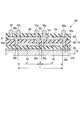
- FIG. 37 is a cross-sectional view of the resin multilayer device of FIG. 36 when viewed in a cross-section in the transmission line width direction.
- FIG. 37 is a cross-sectional view of the resin multilayer device of FIG. 36 when viewed in a cross section in the transmission path length direction.
- FIG. 37 is a schematic circuit diagram for explaining the operation of the multilayer balun formed in the resin multilayer device of FIG. 36. It is sectional drawing at the time of seeing in the cross section of the transmission-line width direction explaining the manufacturing procedure of the resin multilayer device of FIG.
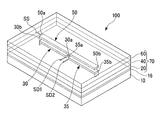
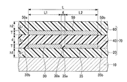
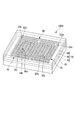
- FIG. 1 is a perspective view schematically showing a configuration example of a resin multilayer device 100 according to the first embodiment of the present invention.
- the resin multilayer device 100 includes a substrate 10, a GND layer 16, a first resin layer 20, a first balanced signal transmission path 30, a second balanced signal transmission path 35, and a second resin.
- the WLP includes the layer 40, one unbalanced signal transmission path 50, and the third resin layer 60.
- the first resin layer 20, the balanced signal transmission paths 30, 35, the second resin layer 40, the unbalanced signal transmission path 50, and the third resin layer 60 are formed of a laminated balun. It is composed.
- the first resin layer 20, the second resin layer 40, and the third resin layer 60 constitute a multilayer resin body 70.
- the substrate 10 is, for example, a semiconductor substrate such as a silicon (Si) substrate, a glass substrate, or an insulating substrate such as GaAs.
- the resin multilayer device 100 is a WLP obtained by monolithic balun.
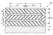
- FIG. 2 is a cross-sectional view of the resin multilayer device 100 when viewed in a cross section in the transmission line width direction.
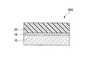
- the GND layer 16 is formed on the substrate 10.
- the first resin layer 20 is formed on the GND layer 16.
- FIG. 3 is a cross-sectional view of the resin multilayer device 100 as seen in a cross section in the transmission path length direction. When the substrate 10 is an insulating substrate, the GND layer 16 may be formed under the substrate 10.
- FIG. 4 is a cross-sectional view of the resin multilayer device 100 when viewed from a cross section in the transmission line width direction when the GND layer 16 is formed under the substrate 10.
- the GND layer 16 is formed under the substrate 10.
- the first resin layer 20 is formed on the substrate 10.
- a fluorine resin such as polyimide resin, epoxy resin, tetrafluoroethylene, or photosensitive resin such as BCB (benzocyclobutene) is used.
- the first balanced signal transmission path 30 and the second balanced signal transmission path 35 are formed on the first resin layer 20.
- the second resin layer 40 is formed on the first resin layer 20.
- a polyimide resin, an epoxy resin, a fluorine resin such as tetrafluoroethylene, or a photosensitive resin such as BCB (benzocyclobutene) is used as the second resin layer 40.
- the third resin layer 60 is formed on the second resin layer 40.
- a polyimide resin for example, a polyimide resin, an epoxy resin, a fluorine resin such as tetrafluoroethylene, or a photosensitive resin such as BCB (benzocyclobutene) is used.
- first resin layer 20, the second resin layer 40, and the third resin layer 60 have the same relative dielectric constant Er by forming the same material using the same method.
- the first balanced signal transmission path 30 and the second balanced signal transmission path 35 are formed on the first resin layer 20.
- the first balanced signal transmission line 30 is a straight transmission line without bending and bending.
- the second balanced signal transmission line 35 is a straight transmission line without bending and bending.
- the first balanced signal transmission path 30 and the second balanced signal transmission path 35 are arranged so as to be coaxial in the longitudinal direction.
- the one end 30a of the first balanced signal transmission path 30 and the one end 35a of the second balanced signal transmission path 35 face each other with an interval g (see FIG. 3).
- One end 30a of the first balanced signal transmission path 30 and one end 35a of the second balanced signal transmission path 35 are signal input / output ends of the balanced signals (differential signals) SD1 and SD2, respectively.
- the other end 30b of the path 30 and the other end 35b of the second balanced signal transmission path 35 are both ground ends and are connected to the GND layer.
- the first balanced signal transmission line 30 and the second balanced signal transmission line 35 are preferably formed to have the same width W and the same thickness T.
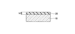
- interval of the lower surface of the 1st balanced signal transmission path 30 and the 2nd balanced signal transmission path 35, and the upper surface of the GND layer 16, ie, the layer thickness of the 1st resin layer 20, is h1 (refer FIG. 2).
- the unbalanced signal transmission path 50 is formed on the second resin layer 40.
- the unbalanced signal transmission line 50 is a straight transmission line that is provided with its lower surface facing the upper surfaces of the first balanced signal transmission line 30 and the second balanced signal transmission line 35 and has no bending or bending. .
- the one end 50a of the unbalanced signal transmission path 50 is a signal input / output end of the unbalanced signal SS, and the other end 50b of the unbalanced signal transmission path 50 is an open end.
- the unbalanced signal transmission path 50 is made of a plated metal such as copper plating.
- the unbalanced signal transmission line 50 is preferably formed of the same metal material by the same formation method as the first balanced signal transmission line 30 and the second balanced signal transmission line 35.
- the unbalanced signal transmission line 50 has a length L of a transmission line length L1 of the balanced signal transmission line 30, a transmission line length L2 of the balanced signal transmission line 35, and a signal input / output terminal 30a of the balanced signal transmission line 30. It is desirable that the total length of the balanced signal transmission line 35 and the distance g of the signal input / output end 35a is the same (see FIG. 3).
- the unbalanced signal transmission line 50 is generally the same width W and the same thickness T as the first balanced signal transmission line 30 and the second balanced signal transmission line 35, but is somewhat different. However, there is no problem in the operation of the balun (see FIG. 2).
- positioned facing through the 2nd resin layer 40, and the upper surface of the 1st balanced signal transmission path 30 and the 2nd balanced signal transmission path 35 is d.
- the distance from the upper surface of the unbalanced signal transmission path 50 to the upper surface of the third resin layer 60 is h2 (see FIG. 2).
- the thickness of the first resin layer 20, the thickness of the second resin layer 40, and the thickness of the third resin layer 60 may be different. Specifically, the first resin layer 20 may be thicker than the second resin layer 40, and the second resin layer 40 may be thicker than the third resin layer 60.
- the distance d between the upper surfaces of the second balanced signal transmission lines 35 and the distance h2 from the upper surface of the unbalanced signal transmission path 50 to the upper surface of the third resin layer 60 may be set as h1> d> h2.
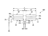
- FIG. 5 is a schematic circuit diagram for explaining the operation of the laminated balun 80 formed in the resin multilayer device 100.
- an unbalanced signal (single signal) SS is input to the signal input / output terminal 50 a of the unbalanced signal transmission path 50, and the signal input / output terminal 30 a of the first balanced signal transmission path 30 and the second balanced signal transmission path 50.
- the balanced signals (differential signals) SD1 and SD2 are output from the signal input / output terminal 35a of the signal transmission path 35, respectively.
- ZS represents the input impedance of the unbalanced signal transmission line 50
- ZD1 and ZD2 represent the output impedances of the balanced signal transmission lines 30 and 35, respectively.
- the balun 80 brings the first balanced signal transmission path 30, the second balanced signal transmission path 35, and the unbalanced signal transmission path 50 close to each other through the second resin layer 40 (see FIG. 1 and the like). By arranging them, the first balanced signal transmission line 30, the second balanced signal transmission line 35, and the unbalanced signal transmission line 50 are electromagnetically coupled.
- the balun 80 converts the unbalanced signal SS into balanced signals (differential signals) SD1 and SD2.
- the signal is output from the signal input / output end 30 a of the first balanced signal transmission path 30 and the signal input / output end 35 a of the second balanced signal transmission path 35.
- balanced signals SD1 and SD2 are input to the signal input / output end 30a of the first balanced signal transmission path 30 and the signal output / input end 35a of the second balanced signal transmission path 35, respectively.
- the signals SD1 and SD2 are converted into an unbalanced signal SS and output from the signal input / output terminal 50a of the unbalanced signal transmission path 50.
- the transmission line length L1 of the balanced signal transmission line 30 and the transmission line length L2 of the balanced signal transmission line 35 are each ⁇ / 4, and unbalanced signal transmission is performed.
- Such a balun needs to be converted to a balanced signal when demodulating an unbalanced signal received by the antenna, and is required to be converted to an unbalanced signal when transmitting a modulated signal that is a balanced signal from the antenna.
- a wireless communication device such as a telephone, it is an indispensable circuit.
- the balun 80 in FIG. 5 also has a function as a transformer for converting the impedance value.
- the input impedance ZS on the unbalanced signal side (single signal input side) and the output impedances ZD1 and ZD2 on the balanced signal side (differential signal output side) are required to be impedance values of design specifications.
- the input / output impedance value of the modem circuit and the output impedance value of the antenna do not necessarily match. For this reason, a balun having an impedance conversion function is indispensable in order to match both impedance values. If the balun is not inserted between the two, or if the input / output impedance value of the balun deviates from the design value even if it is inserted, another impedance converter is required.
- FIGS. 6 to 11 illustrate a procedure for forming a balun on the GND layer 16 on the substrate 10 in the manufacturing procedure of the resin multilayer device 100.
- the substrate 10 is a silicon (Si) wafer in which an IC is formed by a CMOS process or the like.
- the resin multilayer device 100 is a WLP
- the balun is a WLCSP technology (a technology in which a rewiring layer is formed on a wafer by a resin layer forming process and a wiring forming process such as thick film copper wiring, and then dicing into a chip) Is formed on the silicon wafer.
- the GND layer 16 is formed on the substrate 10 by sputtering of Al or the like in a CMOS process or the like.
- a first resin layer 20 is formed on a substrate 10 that is a silicon wafer, and a GND layer 11 a of an IC built in the substrate 10 is formed on the first resin layer 20. Openings 21a and 21b for opening 11b and openings 22a and 22b for opening balanced signal (differential signal) input pads 12a and 12b of the IC are provided.
- a photosensitive insulating resin having a relative dielectric constant Er is used as the first resin layer 20 a photosensitive insulating resin having a relative dielectric constant Er is used.
- the fluid resin material of the photosensitive resin is coated on the substrate 10 by a spin coating method to form a photosensitive resin layer having a thickness dimension h1. And opening part 21a, 21b, 22a, 22b is provided in this photosensitive resin layer by the photolithographic method.
- the openings 21a and 21b are for contacting the ground end 30b of the balanced signal transmission path 30 and the ground end 35b of the balanced signal transmission path 35 to the GND layers 11a and 11b, respectively. Further, the openings 22a and 22b contact the signal output / input end 30a of the balanced signal transmission path 30 and the signal output / input end 35a of the balanced signal transmission path 35 with the balanced signal (differential signal) input pads 12a and 12b of the IC. It is for making it happen.
- the first balanced signal transmission path 30 and the second balanced signal transmission path 35 are provided on the first resin layer 20.
- Copper plating is used for the first balanced signal transmission line 30 and the second balanced signal transmission line 35.
- a resist is formed and patterned by a photolithography method, then copper plating is performed, and this copper plating layer is patterned by an etching method to obtain a width dimension W and a thickness.
- connection wiring 31a which electrically connects between the signal output / input end 30a of the first balanced signal transmission path 30 and the balanced signal input pad 12a, the ground end 30b of the first balanced signal transmission path 30, and the GND layer 11a.
- a connection wiring 36b that electrically connects the ground end 35b of the path 35 and the GND layer 11b is formed.
- the second resin layer 40 is formed on the first resin layer 20 provided with the first balanced signal transmission path 30 and the second balanced signal transmission path 35.
- a photosensitive insulating resin having the same dielectric constant Er as that of the first resin layer 20 is used as the second resin layer 40.
- the photosensitive resin fluid resin material is coated on the first resin layer 20 provided with the first balanced signal transmission path 30 and the second balanced signal transmission path 35 by spin coating, and the upper surface of the balanced signal transmission path 30 is coated. Then, a photosensitive resin layer having a thickness d from the upper surface of the balanced signal transmission path 35 is formed.
- an unbalanced signal transmission path 50 is provided on the second resin layer 40.
- the same copper plating as that of the first balanced signal transmission path 30 and the second balanced signal transmission path 35 is used.
- a resist is formed and patterned by a photolithography method, then copper plating is performed, and this copper plating layer is patterned by an etching method to obtain a width dimension W and a thickness.
- the unbalanced signal transmission line 50 having the dimension T and the length dimension L, and the connection wiring 51 for electrically connecting the signal input / output end 50a of the unbalanced signal transmission line 50 to a mounting substrate or the like are formed.
- a third resin layer 60 serving as a sealing resin layer is formed on the second resin layer 40 provided with the unbalanced signal transmission path 50, and an opening exposing the connection wiring 51 is formed in the third resin layer 60.
- a portion 61 is provided.
- a photosensitive insulating resin having the same dielectric constant Er as that of the first resin layer 20 and the second resin layer 40 is used as the third resin layer 60.
- the fluid resin material of the photosensitive resin is coated on the second resin layer 40 provided with the unbalanced signal transmission path 50 by spin coating, and the photosensitive resin having a thickness h2 from the upper surface of the unbalanced signal transmission path 50 is coated. Form a layer.
- the opening part 61 is provided in this photosensitive resin layer by the photolithographic method.
- solder bump for connecting the connection wiring 51 to a signal output pad such as a mounting substrate is provided in the opening 61.
- the substrate 10 which is a silicon wafer is diced to obtain a WLP resin multilayer device 100.
- the first balanced signal transmission path 30, the second balanced signal transmission path 35, and the unbalanced signal transmission path 50 are preferably formed by copper bright plating. Further, in addition to the bright plating of copper, it can be formed by bright plating of nickel (Ni), gold (Au), silver (Ag) or the like.
- Ni nickel
- Au gold
- Ag silver
- the skin effect For example, for a signal with a frequency of 10 GHz, the skin depth of copper is 0.66 ⁇ m.
- the skin depth of copper is 0.27 ⁇ m. For this reason, if the surface of the transmission path is uneven, the current flows through a longer path than when the surface is flat. Therefore, if there are irregularities on the surface of the transmission line, the balun passage loss will increase. By using bright plating that can flatten the surface of the transmission path, the balun passage loss can be reduced.
- the GND layer 16, the first resin layer 20, the first balanced signal transmission path 30, the second balanced signal transmission path 35, and the second resin are formed on the substrate 10.
- the WLCSP technology is a resin with the same high accuracy as the CMOS semiconductor processing technology. Since a low resistance transmission line can be formed by layer and copper plating, etc., a high-precision input / output impedance and a low insertion loss balun can be obtained, and when an IC is formed on the substrate, The balun can be made monolithic.
- the required number of layers can be reduced as compared with the case where the balun is manufactured by the LTCC technique, so that it can be manufactured more easily.
- the GND layer for grounding the ground end 30b of the first balanced signal transmission path 30 and the ground end 35b of the second balanced signal transmission path 35 is formed on the substrate 10. It is connected to the GND layer of the IC and the GND layer of the printed circuit board.
- the balun by configuring the balun with a transmission path such as a multilayer resin and copper plating, it is possible to reduce the weight of the balun, improve impact resistance, and improve heat dissipation.
- Si when used for the substrate, it can be thinned by grinding Si from the back surface, and can also be used by being incorporated in the substrate.
- FIG. 12 is a cross-sectional view illustrating a resin multilayer device 101 according to Modification 1 of the first embodiment when viewed in a cross section in the transmission line width direction.
- FIG. 13 is a cross-sectional view illustrating a resin multilayer device 101 according to Modification 1 of the first embodiment when viewed in a cross section in the transmission path length direction. 12 and 13, the same reference numerals are given to the same components as those in FIGS.
- the resin multilayer device 101 according to the first modification of the first embodiment includes a substrate 10, a first GND layer 16, a first resin layer 20, a first balanced signal transmission path 30, and a second balanced signal transmission.
- the WLP includes a path 35, a second resin layer 40, an unbalanced signal transmission path 50, a third resin layer 60, and a second GND layer 66.
- the resin multilayer device 101 of FIG. 12 and FIG. 13 is the one in which the second GND layer 66 is provided on the third resin layer 60 in the resin multilayer device 100 of the first embodiment (see FIGS. 1 to 4). It is.
- the first GND layer 16 is formed by, for example, copper plating, an aluminum film, or a copper film
- the second GND layer 66 is formed by, for example, copper plating, an aluminum film, or a copper film.
- the multilayer resin body It is necessary to provide a through-conductive via hole in 70 to connect between the first GND layer 16 and the second GND layer 66. Thereby, the first GND layer 16 and the second GND layer 66 can be kept at the same potential.
- the first GND layer 16 and the second balanced signal transmission line 30 and the unbalanced signal transmission line 50 are placed above and below the first balanced signal transmission line 35 and the unbalanced signal transmission line 50 in this way.
- the characteristics of the balun become a problem of the internal electromagnetic field surrounded by the first GND layer 16 and the second GND layer 66.
- the influence from the circuit can be reduced and it is not affected by external environmental changes.
- FIG. 14 is a cross-sectional view illustrating a resin multilayer device 102 according to Modification 2 of the first embodiment when viewed in a cross section in the transmission path length direction.
- the resin multilayer device 102 of Modification 2 of the first embodiment includes a substrate 10, a GND layer 16, a first resin layer 20, a first balanced signal transmission path 30, and a second balanced signal transmission path 35.
- the WLP includes the second resin layer 40, the unbalanced signal transmission path 50, the third resin layer 60, and the solder bumps 33a, 33b, 38a, 38b, and 52.
- the resin multilayer device 102 of FIG. 14 is the same as the resin multilayer device 100 of the first embodiment (see FIGS. 1 to 4), but the solder bump for flip chip mounting or the like is formed in the opening formed in the third resin layer 60. 33a, 33b, 38a, 38b, 52 are provided.
- the solder bump 33a is an input / output terminal for the balanced signal SD1 (see FIG. 1 or FIG. 5), and is connected to the signal output / input end 30a of the first balanced signal transmission line 30 via the connection wiring 32a.
- the solder bump 38a is an input / output terminal for the balanced signal SD2 (see FIG. 1), and is connected to the signal output / input end 35a of the second balanced signal transmission path 35 via the connection wiring 37a.
- the solder bump 52 is connected to the signal input / output end 50 a of the unbalanced signal transmission path 50 through the connection wiring 51.
- solder bump 33b is a ground terminal, and is connected to the ground end 30b of the first balanced signal transmission path 30 through the connection wiring 32b.
- solder bump 38b is a ground terminal, and is connected to the ground end 35b of the second balanced signal transmission path 35 via the connection wiring 37b.
- FIG. 15 is a perspective view schematically showing a configuration example of the resin multilayer device 200 according to the second embodiment of the present invention.
- the resin multilayer device 200 of the second embodiment includes a substrate 10, a first resin layer 20, a first balanced signal transmission path 30 and a second balanced signal transmission path 35, each provided in a planar spiral shape
- the WLP includes a second resin layer 40, an unbalanced signal transmission path 50 provided in a planar spiral shape, and a third resin layer 60.
- the resin multilayer device 200 of the second embodiment in FIG. 15 includes the first balanced signal transmission path 30 and the second balanced signal transmission path 35 (see FIG. 1) formed straight in the first embodiment.
- the first balanced signal transmission path 30 and the second balanced signal transmission path 35 are respectively spiral type, and the unbalanced signal transmission path 50 (see FIG. 1) formed straight in the first embodiment is also used. Accordingly, a spiral unbalanced signal transmission path 50 is formed. Accordingly, the spiral-type first balanced signal transmission path 30 and the second balanced signal transmission path 35 are opposed to the spiral-type first balanced signal transmission path 30 and the second balanced signal transmission path 35.
- the arranged spiral type unbalanced signal transmission path 50 is electromagnetically coupled to form a laminated type balun.
- the balun of the second embodiment is also laminated as a transmission path such as copper plating in the multilayer resin body 70 on the GND layer 16 on the substrate 10 as in the first embodiment.
- first balanced signal transmission path 30, the second balanced signal transmission path 35, and the unbalanced signal transmission path 50 are straight types as in the first embodiment, no space is required in the width direction of the transmission path. However, a space longer than the transmission path length of the unbalanced signal transmission path 50 is required in the length direction of the transmission path. However, in a few GHz band application, it is often difficult in practice to secure such a long space on the resin multilayer device.
- the first balanced signal transmission path 30, the second balanced signal transmission path 35, and the unbalanced signal transmission path 50 are provided in a spiral shape so that they are long in a narrow space such as a rectangle or an ellipse.
- the first balanced signal transmission path 30, the second balanced signal transmission path 35, and the unbalanced signal transmission path 50 of the transmission path length can be arranged. For this reason, by using a spiral type, it is possible to reduce the space occupied by the balun and realize a balun having a long transmission path.
- a planar spiral formed by the first balanced signal transmission path 30 provided on the first resin layer 20 is the first spiral
- a planar spiral formed by the second balanced signal transmission path 35 provided on the first resin layer 20 is the first.
- the unbalanced signal transmission path 50 provided on the second resin layer 40 is formed as a single transmission path by drawing two spirals along the first and second spirals. Yes.
- the outer peripheral end of the first balanced signal transmission path 30 is a signal input / output end 30a of the balanced signal SD1, and the inner peripheral end of the first balanced signal transmission path 30 is a ground end 30b. ing.
- the first spiral forms a clockwise spiral from the inner peripheral end toward the outer peripheral end when viewed from the upper side of the resin multilayer device 200.
- the outer peripheral end of the second balanced signal transmission path 35 is a signal output / input end 35a of the balanced signal SD2, and the inner peripheral end of the second balanced signal transmission path 35 is a ground terminal. 35b.
- the second spiral forms a counterclockwise spiral from the inner peripheral end toward the outer peripheral end when viewed from the upper side of the resin multilayer device 200.
- the first spiral forms a counterclockwise spiral from the inner peripheral end to the outer peripheral end, and the second spiral rotates clockwise from the inner peripheral end to the outer peripheral end. It may be a spiral.
- the spiral-type unbalanced signal transmission path 50 is formed in the first spiral in the clockwise direction from the inner peripheral end to the outer peripheral end so as to face the first balanced signal transmission path 30. Is formed counterclockwise from the inner peripheral end to the outer peripheral end so as to face the second balanced signal transmission line 35, and the outer peripheral end of the first spiral and the outer peripheral end of the second spiral are connected to each other. Thus, one transmission line is formed.
- the inner peripheral end on the first spiral side of the unbalanced signal transmission path 50 is a signal input / output end 50a for the unbalanced signal SS, and the inner peripheral end on the second spiral side of the unbalanced signal transmission path 50 is The open end 50b.
- the unbalanced signal transmission path 50 is a counterclockwise spiral from the inner peripheral end toward the outer peripheral end facing the balanced signal transmission path 30 in the first spiral when viewed from the upper side of the resin multilayer device 200.
- a clockwise spiral may be formed from the inner peripheral end toward the outer peripheral end facing the balanced signal transmission path 35.
- the same effect as that of the first embodiment can be obtained, and the transmission path length can be increased by providing the transmission path constituting the balun in a spiral shape.
- the space occupied by the balun can be reduced.
- the manufacturing procedure of the resin multilayer device 200 of the second embodiment is the same as that of the first embodiment.
- FIG. 16 is a perspective view schematically showing a configuration example of the resin multilayer device 300 according to the third embodiment of the present invention.
- the resin multilayer device 300 according to the third embodiment includes a substrate 10, a GND layer 16, a first resin layer 20, a first balanced signal transmission path 30 and a second balanced signal transmission provided in a meander type, respectively.
- the WLP includes a path 35, a second resin layer 40, an unbalanced signal transmission path 50 provided in a meander shape, and a third resin layer 60.
- the resin multilayer device 300 of the third embodiment in FIG. 16 includes the first balanced signal transmission path 30 and the second balanced signal transmission path 35 (see FIG. 1) formed straight in the first embodiment. These are the meander type first balanced signal transmission line 30 and the second balanced signal transmission line 35, respectively, and the unbalanced signal transmission line 50 (see FIG. 1) formed straight in the first embodiment. Accordingly, the meander type unbalanced signal transmission path 50 is formed.
- the two meander-type first balanced signal transmission lines 30 and the second balanced signal transmission line 35 and the meander-type first balanced signal transmission lines 30 and the second balanced signal transmission lines 35 are opposed to each other.
- the meander-type unbalanced signal transmission line 50 arranged in this manner is electromagnetically coupled to form a laminated balun.
- the balun of the third embodiment is also laminated as a transmission path such as copper plating in the multilayer resin body 70 on the GND layer 16 on the substrate 10 as in the first embodiment.
- first balanced signal transmission path 30, the second balanced signal transmission path 35, and the unbalanced signal transmission path 50 are straight types as in the first embodiment, no space is required in the width direction of the transmission path. However, a space longer than the transmission path length of the unbalanced signal transmission path 50 is required in the length direction of the transmission path. However, in a few GHz band application, it is often difficult in practice to secure such a long space on the resin multilayer device.
- the first balanced signal transmission path 30, the second balanced signal transmission path 35, and the unbalanced signal transmission path 50 are provided in a meander type, so that a long transmission path is formed in a narrow space such as a square.
- the long first balanced signal transmission line 30, the second balanced signal transmission line 35, and the unbalanced signal transmission line 50 can be arranged. Therefore, by adopting the meander type, it is possible to reduce the space occupied by the balun and realize a balun having a long transmission path.
- the meander by the first balanced signal transmission line 30 provided on the first resin layer 20 is defined as the first meander, and the meander is also provided by the second balanced signal transmission line 35 provided on the first resin layer 20.
- the meander disposed adjacent to the first meander is the second meander
- the unbalanced signal transmission path 50 provided on the second resin layer 40 is along the first and second meanders. It is formed as a single transmission line as if a meander is drawn.
- the transmission line end of the first balanced signal transmission line 30 located at the corner on the side adjacent to the second meander is the signal input / output end 30a of the balanced signal SD1, and the second meander
- the transmission line end of the first balanced signal transmission line 30 located at the corner not adjacent to the meander is a ground terminal 30b.
- the transmission line end of the second balanced signal transmission line 35 located at the corner on the side adjacent to the first meander is a signal input / output end 35a of the balanced signal SD2
- the transmission line end of the second balanced signal transmission line 35 located at the corner not adjacent to the first meander is a grounding end 35b.
- the meander-type unbalanced signal transmission path 50 is formed in a region on the second resin layer 40 opposite to the first meander and second meander regions on the first resin layer 20 and the first balanced signal transmission path 30 and It is formed as one meander type transmission line so as to face the second balanced signal transmission line 35.
- the transmission line end located on the first meander area of the unbalanced signal transmission path 50 is a signal input / output terminal 50a of the unbalanced signal SS, and the second meander area of the unbalanced signal transmission path 50
- the upper end of the transmission path is an open end 50b.
- the same effect as that of the first embodiment can be obtained, and the transmission path length can be increased by providing the transmission path constituting the balun in a meander type.
- the space occupied by the balun can be reduced.
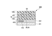
- FIG. 17 is a cross-sectional view illustrating a configuration example of the resin multilayer device 400 according to the fourth embodiment of the present invention when viewed in a cross section in the transmission line width direction.
- the substrate is a CMOS-IC substrate 410.
- the resin multilayer device 400 of the fourth embodiment includes a CMOS-IC substrate 410, a GND layer 16, a first resin layer 20, a first balanced signal transmission path 30, a second balanced signal transmission path 35,
- the WLP includes the second resin layer 40, one unbalanced signal transmission line 50, and the third resin layer 60.
- the CMOS-IC substrate 410 includes a substrate 411 and a SiO 2 layer 412. In the SiO 2 layer 412, an Al or AlCu wiring 413 and an inductor 414 are arranged. A GND layer 16 is provided on the SiO 2 layer 412, but a window is provided in the GND layer 16 on the inductor 414. The structure of the portion above the GND layer 16 is the same as that of the first embodiment.
- the same effect as that of the first embodiment can be obtained, and since the GND layer 16 is not provided on the inductor 414, the characteristics of the inductor provided in the IC can be improved. Deterioration can be prevented.
- FIG. 18 is a cross-sectional view illustrating a configuration example of the resin multilayer device 500 according to the fifth embodiment of the present invention when viewed in a cross section in the transmission line width direction.
- the substrate is a CMOS-IC substrate 410.
- the resin multilayer device 500 of the fifth embodiment includes a CMOS-IC substrate 410, a GND layer 16, a first resin layer 20, a first balanced signal transmission path 30, a second balanced signal transmission path 35,
- the WLP includes the second resin layer 40, one unbalanced signal transmission line 50, and the third resin layer 60.
- the CMOS-IC substrate 410 includes a substrate 411 and a SiO 2 layer 412. Al or AlCu wiring 413 is arranged on the SiO 2 layer 412.
- the difference from the fourth embodiment is that the GND layer 16 is provided not around the SiO 2 layer 412 but around the transmission line.
- the same effects as those of the first and fourth embodiments can be obtained, and the CMOS-IC substrate 410 and the GND layer 16 are separated from each other.
- the influence of the GND layer 16 on the operation of the CMOS-IC substrate 410 is prevented, and a monolithic balun with stable characteristics can be realized.
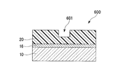
- FIGS. 19 to 26 are sectional views showing a manufacturing procedure of the resin multilayer device 600 according to the sixth embodiment of the present invention when viewed in a section in the transmission line width direction. As shown in FIG. 19, a photosensitive resin is applied on the GND layer 16 on the substrate 10 to form the first resin layer 20.
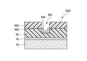
- a recess 601 is formed on the first resin layer 20 by photolithography.
- a seed layer 602 is formed on the first resin layer 20 by sputtering.
- a first layer made of TiW or Cr is formed by sputtering, and a second layer made of Cu is formed thereon.
- the seed layer 602 is generally composed of a laminate of a first layer made of TiW or Cr and a second layer made of Cu, but may be made of other materials.
- a resist 603 is formed by patterning on the seed layer 602 on the portion excluding the recess 601.
- a lower wiring 604 is formed in the recess 601 by performing a plating process.
- the lower wiring 604 corresponds to the first balanced signal transmission path 30 or the second balanced signal transmission path 35.
- the seed layer 602 is removed by etching.
- the second resin layer 40 is formed on the first resin layer 20. Since the lower wiring 604 is formed in the concave portion 601 of the first resin layer 20, the upper portion of the first resin layer 20 becomes flat, and the second resin layer 40 can be formed flat.
- an upper wiring 605 is formed on the second resin layer 40.
- the upper wiring 605 corresponds to the unbalanced signal transmission path 50.
- the method for forming the upper wiring 605 may be the same as the method for forming the unbalanced signal transmission path 50 in the first embodiment.
- the third resin layer 60 is formed on the second resin layer 40.
- the method for forming the third resin layer 60 may be the same as the method for forming the third resin layer 60 in the first embodiment.
- the same effects as those of the first embodiment can be obtained, and high-precision impedance control can be realized by forming the second resin layer 40 flat. Further, by forming the lower wiring 604 in the concave portion 601 and forming the concave shape, the surface area of the lower wiring 604 is increased, and the resistance of the lower wiring 604 can be reduced.
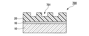
- FIGS. 27 to 31 are sectional views showing a manufacturing procedure of the resin multilayer device 700 according to the seventh embodiment of the present invention when viewed in a section in the transmission line width direction.
- a photosensitive resin is applied on the GND layer 16 on the substrate 10 to form the first resin layer 20, and then, as shown in FIG. As a result, a plurality of recesses 701 are formed in the upper part of the first resin layer 20.
- a resist 603 is formed by patterning as shown in FIG.
- a plurality of lower wirings 704 are formed in the plurality of recesses 701 by performing a plating process.
- a metal layer 705 is formed by sputtering, and a plurality of lower wirings 704 are electrically connected.
- the seed layer 602 is removed by etching.
- the second resin layer 40 is formed on the first resin layer 20, and the upper wiring 605 is formed on the second resin layer 40.
- the third resin layer 60 is formed on the second resin layer 40.
- the same effect as in the first embodiment and the sixth embodiment can be obtained, and the aspect ratio of the lower wiring 704 can be reduced by providing a plurality of recesses. And the dent of the second resin layer 40 on the lower wiring 704 provided in the recess can be reduced. By forming the second resin layer 40 to be flatter, more accurate impedance control can be realized.
- FIG. 32 is a cross-sectional view showing a manufacturing procedure of the resin multilayer device 750 according to Modification 1 of the seventh embodiment of the present invention when viewed in a cross-section in the transmission line width direction.
- the difference from the sixth embodiment is that the upper wiring 605 is made concave instead of the lower wiring 604.
- the manufacturing procedure of the concave upper wiring 605 is the same as the manufacturing method of the lower wiring 704 of the seventh embodiment.
- FIGS. 33 and 34 are sectional views showing a manufacturing procedure of the resin multilayer device 770 according to Modification 2 of the seventh embodiment of the present invention when viewed in a section in the transmission line width direction.
- a resin is applied on the GND layer 16 on the substrate 10 to form the first resin layer 20.
- this resin may not be photosensitive.
- a photosensitive resin layer 771 is newly formed on the first resin layer 20 to form a recess.
- the same effects as those of the sixth embodiment and the seventh embodiment can be obtained, and it is necessary to form a recess in the first resin layer 20. Therefore, the height h1 of the first resin layer 20 can be increased, and the wiring thickness can be increased.
- FIG. 35 is a cross-sectional view illustrating a configuration example of the resin multilayer device 800 according to the eighth embodiment of the present invention when viewed in a cross section in the transmission line width direction.
- the resin multilayer device 800 according to the eighth embodiment includes a substrate 10, a GND layer 16, a first resin layer 20, a first balanced signal transmission path 30, a second balanced signal transmission path 35, and a second resin.
- the WLP includes the layer 40, one unbalanced signal transmission path 50, and the third resin layer 60.
- the difference of the eighth embodiment from the first embodiment is that, in the eighth embodiment, the first balanced signal transmission path 30, the second balanced signal transmission path 35, and the unbalanced signal transmission path 50 are used. Are shifted so that there are few overlapping portions. As a result, the wiring width can be increased without reducing the impedance, so that balun loss can be suppressed.
- the manufacturing method of the first balanced signal transmission path 30 and the second balanced signal transmission path 35 is similar to the sixth embodiment or the seventh embodiment.
- a balanced signal transmission line 30 and a second balanced signal transmission line 35 are formed. Thereby, an offset lamination can be manufactured with high accuracy.
- FIG. 36 is a perspective view schematically showing a configuration example of the resin multilayer device 900 according to the ninth embodiment of the present invention.
- FIG. 37 is a cross-sectional view of the resin multilayer device 900 as seen in a cross section in the transmission line width direction.
- FIG. 38 is a cross-sectional view of the resin multilayer device 900 when viewed in a cross-section in the transmission path length direction.
- the resin multilayer device 900 of the ninth embodiment includes a substrate 10, a first resin layer 20, a first balanced signal transmission path 30, a second balanced signal transmission path 35, a second resin layer 40, 1
- the WLP is configured to include an unbalanced signal transmission line 50 and a third resin layer 60.
- the first resin layer 20, the balanced signal transmission paths 30, 35, the second resin layer 40, the unbalanced signal transmission path 50, and the third resin layer 60 are formed of a laminated balun. It is composed.
- the first resin layer 20, the second resin layer 40, and the third resin layer 60 constitute a multilayer resin body 70.
- the substrate 10 is, for example, a semiconductor substrate such as a silicon (Si) substrate, a glass substrate, or an insulating substrate such as GaAs.
- the resin multilayer device 900 is a WLP obtained by monolithic balun.
- First resin layer 20, second resin layer 40, third resin layer 60 As the first resin layer 20, for example, a polyimide resin, an epoxy resin, a fluorine resin such as tetrafluoroethylene, or a photosensitive resin such as BCB (benzocyclobutene) is used.
- the first balanced signal transmission path 30 and the second balanced signal transmission path 35 are formed on the first resin layer 20.
- the second resin layer 40 is formed on the first resin layer 20.
- a polyimide resin, an epoxy resin, a fluorine resin such as tetrafluoroethylene, or a photosensitive resin such as BCB (benzocyclobutene) is used as the second resin layer 40.
- the third resin layer 60 is formed on the second resin layer 40.
- a polyimide resin for example, a polyimide resin, an epoxy resin, a fluorine resin such as tetrafluoroethylene, or a photosensitive resin such as BCB (benzocyclobutene) is used.
- first resin layer 20, the second resin layer 40, and the third resin layer 60 have the same relative dielectric constant Er by forming the same material using the same method.
- the first balanced signal transmission path 30 and the second balanced signal transmission path 35 are formed on the first resin layer 20.
- the first balanced signal transmission line 30 is a straight transmission line without bending and bending.
- the second balanced signal transmission line 35 is a straight transmission line without bending and bending.
- the first balanced signal transmission path 30 and the second balanced signal transmission path 35 are arranged so as to be coaxial in the longitudinal direction.
- the one end 30a of the first balanced signal transmission path 30 and the one end 35a of the second balanced signal transmission path 35 face each other with an interval g (see FIG. 38).
- One end 30a of the first balanced signal transmission path 30 and one end 35a of the second balanced signal transmission path 35 are signal input / output ends of the balanced signals (differential signals) SD1 and SD2, respectively.
- the other end 30b of the path 30 and the other end 35b of the second balanced signal transmission path 35 are both grounded ends (connected to GND).
- the first balanced signal transmission line 30 and the second balanced signal transmission line 35 are preferably formed to have the same width W and the same thickness T.
- substrate 10, ie, the layer thickness of the 1st resin layer 20, is h1 (refer FIG. 37).
- the unbalanced signal transmission path 50 is formed on the second resin layer 40.
- the unbalanced signal transmission line 50 is a straight transmission line that is provided with its lower surface facing the upper surfaces of the first balanced signal transmission line 30 and the second balanced signal transmission line 35 and has no bending or bending. .
- the one end 50a of the unbalanced signal transmission path 50 is a signal input / output end of the unbalanced signal SS, and the other end 50b of the unbalanced signal transmission path 50 is an open end.
- the unbalanced signal transmission path 50 is made of a plated metal such as copper plating.
- the unbalanced signal transmission line 50 is preferably formed of the same metal material by the same formation method as the first balanced signal transmission line 30 and the second balanced signal transmission line 35.
- the unbalanced signal transmission line 50 has a length L of a transmission line length L1 of the balanced signal transmission line 30, a transmission line length L2 of the balanced signal transmission line 35, and a signal input / output terminal 30a of the balanced signal transmission line 30. It is desirable that the total length of the balanced signal transmission line 35 and the distance g of the signal input / output end 35a be the same (see FIG. 38).
- the unbalanced signal transmission line 50 is generally the same width W and the same thickness T as the first balanced signal transmission line 30 and the second balanced signal transmission line 35, but is somewhat different. However, there is no problem in the operation of the balun (see FIG. 37).
- positioned facing through the 2nd resin layer 40, and the upper surface of the 1st balanced signal transmission path 30 and the 2nd balanced signal transmission path 35 is d.
- the distance from the upper surface of the unbalanced signal transmission path 50 to the upper surface of the third resin layer 60 is h2 (see FIG. 37).
- the thickness of the first resin layer 20, the thickness of the second resin layer 40, and the thickness of the third resin layer 60 may be different. Specifically, the first resin layer 20 may be thicker than the second resin layer 40, and the second resin layer 40 may be thicker than the third resin layer 60.
- the distance d between the upper surfaces of the balanced signal transmission lines 35 and the distance h2 from the upper surface of the unbalanced signal transmission path 50 to the upper surface of the third resin layer 60 may be set as h1> d> h2.
- FIG. 39 is a schematic circuit diagram for explaining the operation of the multilayer balun 980 formed in the resin multilayer device 900.
- an unbalanced signal (single signal) SS is input to the signal input / output terminal 50a of the unbalanced signal transmission path 50, and the signal input / output terminal 30a of the first balanced signal transmission path 30 and the second balanced input / output terminal 50a.
- Balanced signals (differential signals) SD1 and SD2 are output from the signal input / output terminal 35a of the signal transmission path 35, respectively.
- ZS represents the input impedance of the unbalanced signal transmission line 50
- ZD1 and ZD2 represent the output impedances of the balanced signal transmission lines 30 and 35, respectively.
- the balun 980 brings the first balanced signal transmission path 30, the second balanced signal transmission path 35, and the unbalanced signal transmission path 50 close to each other through the second resin layer 40 (see FIG. 36, etc.). By arranging them, the first balanced signal transmission line 30, the second balanced signal transmission line 35, and the unbalanced signal transmission line 50 are electromagnetically coupled.
- the balun 980 converts the unbalanced signal SS into balanced signals (differential signals) SD1 and SD2.
- the signal is output from the signal input / output end 30 a of the first balanced signal transmission path 30 and the signal input / output end 35 a of the second balanced signal transmission path 35.
- balanced signals SD1 and SD2 are input to the signal input / output end 30a of the first balanced signal transmission path 30 and the signal output / input end 35a of the second balanced signal transmission path 35, respectively.
- the signals SD1 and SD2 are converted into an unbalanced signal SS and output from the signal input / output terminal 50a of the unbalanced signal transmission path 50.
- the transmission line length L1 of the balanced signal transmission line 30 and the transmission line length L2 of the balanced signal transmission line 35 are each ⁇ / 4, and unbalanced signal transmission is performed.
- Such a balun needs to be converted to a balanced signal when demodulating an unbalanced signal received by the antenna, and is required to be converted to an unbalanced signal when transmitting a modulated signal that is a balanced signal from the antenna.
- a wireless communication device such as a telephone, it is an indispensable circuit.
- the balun 980 shown in FIG. 39 also has a function as a transformer for converting the impedance value.
- the input impedance ZS on the unbalanced signal side (single signal input side) and the output impedances ZD1 and ZD2 on the balanced signal side (differential signal output side) are required to be impedance values of design specifications.
- the input / output impedance value of the modem circuit and the output impedance value of the antenna do not necessarily match. For this reason, a balun having an impedance conversion function is indispensable in order to match both impedance values. If the balun is not inserted between the two, or if the input / output impedance value of the balun deviates from the design value even if it is inserted, another impedance converter is required.
- FIGS. 40 to 45 illustrate a procedure for forming a balun on the substrate 10 in the manufacturing procedure of the resin multilayer device 900.
- the substrate 10 is a silicon (Si) wafer in which an IC is formed by a CMOS process or the like.
- the resin multilayer device 900 is a WLP
- the balun uses WLCSP technology (a technology in which a rewiring layer is formed on a wafer by a resin layer forming process and a wiring forming process such as thick film copper wiring, and then dicing into chips) Is formed on the silicon wafer.
- a first resin layer 20 is formed on a substrate 10 that is a silicon wafer, and the GND layers 11a of the ICs built in the substrate 10 are formed on the first resin layer 20. Openings 21a and 21b for opening 11b and openings 22a and 22b for opening balanced signal (differential signal) input pads 12a and 12b of the IC are provided.
- a photosensitive insulating resin having a relative dielectric constant Er is used as the first resin layer 20.
- the fluid resin material of the photosensitive resin is coated on the substrate 10 by a spin coating method to form a photosensitive resin layer having a thickness dimension h1.
- opening part 21a, 21b, 22a, 22b is provided in this photosensitive resin layer by the photolithographic method.
- the openings 21a and 21b are for contacting the ground end 30b of the balanced signal transmission path 30 and the ground end 35b of the balanced signal transmission path 35 to the GND layers 11a and 11b, respectively. Further, the openings 22a and 22b contact the signal output / input end 30a of the balanced signal transmission path 30 and the signal output / input end 35a of the balanced signal transmission path 35 with the balanced signal (differential signal) input pads 12a and 12b of the IC. It is for making it happen.
- the first balanced signal transmission path 30 and the second balanced signal transmission path 35 are provided on the first resin layer 20.
- Copper plating is used for the first balanced signal transmission line 30 and the second balanced signal transmission line 35.
- a resist is formed and patterned by a photolithography method, then copper plating is performed, and this copper plating layer is patterned by an etching method to obtain a width dimension W and a thickness.
- connection wiring 31a which electrically connects between the signal output / input end 30a of the first balanced signal transmission path 30 and the balanced signal input pad 12a, the ground end 30b of the first balanced signal transmission path 30, and the GND layer 11a.
- a connection wiring 36b that electrically connects the ground end 35b of the path 35 and the GND layer 11b is formed.
- the second resin layer 40 is formed on the first resin layer 20 provided with the first balanced signal transmission path 30 and the second balanced signal transmission path 35.
- a photosensitive insulating resin having the same dielectric constant Er as that of the first resin layer 20 is used as the second resin layer 40.
- the photosensitive resin fluid resin material is coated on the first resin layer 20 provided with the first balanced signal transmission path 30 and the second balanced signal transmission path 35 by spin coating, and the upper surface of the balanced signal transmission path 30 is coated. Then, a photosensitive resin layer having a thickness d from the upper surface of the balanced signal transmission path 35 is formed.
- an unbalanced signal transmission path 50 is provided on the second resin layer 40.
- the same copper plating as that of the first balanced signal transmission path 30 and the second balanced signal transmission path 35 is used.
- a resist is formed and patterned by a photolithography method, then copper plating is performed, and this copper plating layer is patterned by an etching method to obtain a width dimension W and a thickness.
- the unbalanced signal transmission line 50 having the dimension T and the length dimension L, and the connection wiring 51 for electrically connecting the signal input / output end 50a of the unbalanced signal transmission line 50 to a mounting substrate or the like are formed.
- a third resin layer 60 serving as a sealing resin layer is formed on the second resin layer 40 provided with the unbalanced signal transmission path 50, and an opening exposing the connection wiring 51 is formed in the third resin layer 60.
- a portion 61 is provided.
- a photosensitive insulating resin having the same dielectric constant Er as that of the first resin layer 20 and the second resin layer 40 is used as the third resin layer 60.
- the fluid resin material of the photosensitive resin is coated on the second resin layer 40 provided with the unbalanced signal transmission path 50 by spin coating, and the photosensitive resin having a thickness h2 from the upper surface of the unbalanced signal transmission path 50 is coated. Form a layer.
- the opening part 61 is provided in this photosensitive resin layer by the photolithographic method.
- connection wiring 51 When the resin multilayer device 900 is flip-chip mounted, a solder bump for connecting the connection wiring 51 to a signal output pad such as a mounting board is provided in the opening 61.
- a solder bump for connecting the connection wiring 51 to a signal output pad such as a mounting board is provided in the opening 61.
- a thin film such as Ni / Au or Al on the connection wiring 51.
- the substrate 10 which is a silicon wafer is diced to obtain a WLP resin multilayer device 900.
- the first balanced signal transmission path 30, the second balanced signal transmission path 35, and the unbalanced signal transmission path 50 are preferably formed by copper bright plating. Further, in addition to the bright plating of copper, it can be formed by bright plating of nickel (Ni), gold (Au), silver (Ag) or the like.
- Ni nickel
- Au gold
- Au silver
- the skin effect For example, for a signal with a frequency of 10 GHz, the skin depth of copper is 0.66 ⁇ m.
- the skin depth of copper is 0.27 ⁇ m. For this reason, if the surface of the transmission path is uneven, the current flows through a longer path than when the surface is flat. Therefore, if there are irregularities on the surface of the transmission line, the balun passage loss will increase. By using bright plating that can flatten the surface of the transmission path, the balun passage loss can be reduced.
- the first resin layer 20, the first balanced signal transmission path 30, the second balanced signal transmission path 35, the second resin layer 40, and the non-coated layer are formed on the substrate 10.
- the WLCSP technology uses a resin layer and copper plating with the same high accuracy as the CMOS semiconductor processing technology. This makes it possible to form a low-resistance transmission line, etc., so that a high-precision input / output impedance and low insertion loss balun can be obtained, and if an IC is formed on the substrate, the balun is made monolithic can do.
- the required number of layers can be reduced as compared with the case where the balun is manufactured by the LTCC technique, so that it can be manufactured more easily.
- the GND layer for grounding the ground end 30b of the first balanced signal transmission path 30 and the ground end 35b of the second balanced signal transmission path 35 is not provided in the device, Are connected to the GND layer of the IC built in the substrate 10.
- the number of layers is larger than that of the conventional balun provided with the GND layer for grounding the grounding end of the balanced signal transmission line. Can be reduced.
- the balun by configuring the balun with a transmission path such as a multilayer resin and copper plating, it is possible to reduce the weight of the balun, improve impact resistance, and improve heat dissipation.
- Si when used for the substrate, it can be thinned by grinding Si from the back surface, and can also be used by being incorporated in the substrate.
- FIG. 46 is a cross-sectional view illustrating a resin multilayer device 901 according to Modification 1 of the ninth embodiment when viewed in a cross section in the transmission line width direction.
- FIG. 47 is a cross-sectional view illustrating a resin multilayer device 901 according to Modification 1 of the ninth embodiment when viewed in a cross section in the transmission path length direction.
- the resin multilayer device 901 of Modification 1 of the ninth embodiment includes a substrate 10, a first GND layer 16, a first resin layer 20, a first balanced signal transmission line 30, and a second balanced signal transmission.
- the WLP includes a path 35, a second resin layer 40, an unbalanced signal transmission path 50, a third resin layer 60, and a second GND layer 66.
- the resin multilayer device 901 shown in FIGS. 46 and 47 is the same as the resin multilayer device 900 of the ninth embodiment (see FIGS. 36 to 38).
- the first GND layer 16 is interposed between the substrate 10 and the first resin layer 20.
- the second GND layer 66 is provided on the third resin layer 60.
- the first GND layer 16 is formed by, for example, copper plating, an aluminum film, or a copper film
- the second GND layer 66 is formed by, for example, copper plating, an aluminum film, or a copper film.
- the multilayer resin body It is necessary to provide a through-conductive via hole in 70 to connect between the first GND layer 16 and the second GND layer 66. Thereby, the first GND layer 16 and the second GND layer 66 can be kept at the same potential.
- the first GND layer 16 and the second balanced signal transmission line 30 and the unbalanced signal transmission line 50 are placed above and below the first balanced signal transmission line 35 and the unbalanced signal transmission line 50 in this way.
- the characteristics of the balun become a problem of the internal electromagnetic field surrounded by the first GND layer 16 and the second GND layer 66.
- the influence from the circuit can be reduced and it is not affected by external environmental changes.
- FIG. 48 is a cross-sectional view illustrating a resin multilayer device 902 according to Modification 2 of the ninth embodiment when viewed in a cross section in the transmission path length direction.
- the resin multilayer device 902 of Modification 2 of the ninth embodiment includes a substrate 10, a first resin layer 20, a first balanced signal transmission path 30, a second balanced signal transmission path 35, and a second resin layer. 40, an unbalanced signal transmission path 50, a third resin layer 60, and solder bumps 33a, 33b, 38a, 38b, 52.
- the resin multilayer device 902 of FIG. 48 is the same as that of the resin multilayer device 900 of the ninth embodiment (see FIGS. 36 to 38). Solder bumps for flip chip mounting or the like are formed in the openings formed in the third resin layer 60. 33a, 33b, 38a, 38b, 52 are provided.
- the solder bump 33a is an input / output terminal for the balanced signal SD1 (see FIG. 36 or FIG. 39), and is connected to the signal output / input terminal 30a of the first balanced signal transmission line 30 via the connection wiring 32a.
- the solder bump 38a is an input / output terminal for the balanced signal SD2 (see FIG. 36 or FIG. 39), and is connected to the signal output / input end 35a of the second balanced signal transmission path 35 via the connection wiring 37a.
- the solder bump 52 is connected to the signal input / output end 50 a of the unbalanced signal transmission path 50 through the connection wiring 51.
- solder bump 33b is a ground terminal, and is connected to the ground end 30b of the first balanced signal transmission path 30 through the connection wiring 32b.
- solder bump 38b is a ground terminal, and is connected to the ground end 35b of the second balanced signal transmission path 35 via the connection wiring 37b.
- FIG. 49 is a perspective view schematically showing a configuration example of the resin multilayer device 1000 according to the tenth embodiment of the present invention.
- the resin multilayer device 1000 of the tenth embodiment includes a substrate 10, a first resin layer 20, a first balanced signal transmission path 30 and a second balanced signal transmission path 35 provided in a plane spiral type, respectively.
- the WLP includes the second resin layer 40, an unbalanced signal transmission path 50 provided in a plane spiral shape, and a third resin layer 60.
- the resin multilayer device 1000 of the tenth embodiment of FIG. 49 includes the first balanced signal transmission path 30 and the second balanced signal transmission path 35 (see FIG. 36) formed straight in the ninth embodiment.
- the first balanced signal transmission path 30 and the second balanced signal transmission path 35 are respectively spiral type, and the unbalanced signal transmission path 50 (see FIG. 36) formed straight in the ninth embodiment is also used. Accordingly, a spiral unbalanced signal transmission path 50 is formed. Accordingly, the spiral-type first balanced signal transmission path 30 and the second balanced signal transmission path 35 are opposed to the spiral-type first balanced signal transmission path 30 and the second balanced signal transmission path 35.
- the arranged spiral type unbalanced signal transmission path 50 is electromagnetically coupled to form a laminated type balun. Note that the balun of the tenth embodiment is also laminated and formed as a transmission path such as copper plating in the multilayer resin body 70 on the substrate 10 as in the ninth embodiment.
- first balanced signal transmission path 30, the second balanced signal transmission path 35, and the unbalanced signal transmission path 50 are straight types as in the ninth embodiment, no space is required in the width direction of the transmission path. However, a space longer than the transmission path length of the unbalanced signal transmission path 50 is required in the length direction of the transmission path. However, in a few GHz band application, it is often difficult in practice to secure such a long space on the resin multilayer device.
- the first balanced signal transmission path 30, the second balanced signal transmission path 35, and the unbalanced signal transmission path 50 are provided in a spiral shape so that they are long in a narrow space such as a rectangle or an ellipse.
- the first balanced signal transmission path 30, the second balanced signal transmission path 35, and the unbalanced signal transmission path 50 of the transmission path length can be arranged. For this reason, by using a spiral type, it is possible to reduce the space occupied by the balun and realize a balun having a long transmission path.
- a planar spiral formed by the first balanced signal transmission path 30 provided on the first resin layer 20 is the first spiral
- a planar spiral formed by the second balanced signal transmission path 35 provided on the first resin layer 20 is the first.
- the unbalanced signal transmission path 50 provided on the second resin layer 40 is formed as a single transmission path by drawing two spirals along the first and second spirals. Yes.
- the outer peripheral end of the first balanced signal transmission path 30 is a signal input / output end 30a of the balanced signal SD1, and the inner peripheral end of the first balanced signal transmission path 30 is a ground end 30b. ing.
- the first spiral forms a clockwise spiral from the inner peripheral edge toward the outer peripheral edge when viewed from the upper side of the resin multilayer device 1000.
- the outer peripheral end of the second balanced signal transmission path 35 is a signal output / input end 35a of the balanced signal SD2, and the inner peripheral end of the second balanced signal transmission path 35 is a ground terminal. 35b.
- the second spiral forms a counterclockwise spiral from the inner peripheral end toward the outer peripheral end as viewed from the upper side of the resin multilayer device 1000.
- the first spiral forms a counterclockwise spiral from the inner peripheral end to the outer peripheral end, and the second spiral rotates clockwise from the inner peripheral end to the outer peripheral end. It may be a spiral.
- the spiral-type unbalanced signal transmission path 50 is formed in the first spiral in the clockwise direction from the inner peripheral end to the outer peripheral end so as to face the first balanced signal transmission path 30. Is formed counterclockwise from the inner peripheral end to the outer peripheral end so as to face the second balanced signal transmission line 35, and the outer peripheral end of the first spiral and the outer peripheral end of the second spiral are connected to each other. Thus, one transmission line is formed.
- the inner peripheral end on the first spiral side of the unbalanced signal transmission path 50 is a signal input / output end 50a for the unbalanced signal SS, and the inner peripheral end on the second spiral side of the unbalanced signal transmission path 50 is The open end 50b.
- the unbalanced signal transmission path 50 is a counterclockwise spiral from the inner peripheral end to the outer peripheral end facing the balanced signal transmission path 30 in the first spiral when viewed from the upper side of the resin multilayer device 1000.
- a clockwise spiral may be formed from the inner peripheral end toward the outer peripheral end facing the balanced signal transmission path 35.
- the same effect as in the ninth embodiment can be obtained, and the transmission path length can be increased by providing the transmission path constituting the balun in a spiral shape.
- the space occupied by the balun can be reduced.
- the manufacturing procedure of the resin multilayer device 1000 of the tenth embodiment is the same as that of the ninth embodiment.
- FIG. 50 is a perspective view schematically showing a configuration example of the resin multilayer device 1100 according to the eleventh embodiment of the present invention.
- the resin multilayer device 1100 according to the eleventh embodiment includes a substrate 10, a first resin layer 20, a first balanced signal transmission line 30 and a second balanced signal transmission line 35 provided in a meander type,
- the WLP is configured to include two resin layers 40, a meander-type unbalanced signal transmission path 50, and a third resin layer 60.
- the resin multilayer device 1100 of the eleventh embodiment of FIG. 50 includes the first balanced signal transmission path 30 and the second balanced signal transmission path 35 (see FIG. 36) formed straight in the ninth embodiment.
- the first balanced signal transmission path 30 and the second balanced signal transmission path 35 are respectively meander type, and the unbalanced signal transmission path 50 (see FIG. 36) formed straight in the ninth embodiment is also used.
- the meander type unbalanced signal transmission path 50 is formed.
- the two meander-type first balanced signal transmission lines 30 and the second balanced signal transmission line 35 and the meander-type first balanced signal transmission lines 30 and the second balanced signal transmission lines 35 are opposed to each other.
- the meander-type unbalanced signal transmission line 50 arranged in this manner is electromagnetically coupled to form a laminated balun.
- the balun of the eleventh embodiment is also laminated and formed as a transmission path such as copper plating in the multilayer resin body 70 on the substrate 10 as in the ninth embodiment.
- first balanced signal transmission path 30, the second balanced signal transmission path 35, and the unbalanced signal transmission path 50 are straight types as in the ninth embodiment, no space is required in the width direction of the transmission path. However, a space longer than the transmission path length of the unbalanced signal transmission path 50 is required in the length direction of the transmission path. However, in a few GHz band application, it is often difficult in practice to secure such a long space on the resin multilayer device.
- the ninth balanced signal transmission path 30, the second balanced signal transmission path 35, and the unbalanced signal transmission path 50 are provided in a meander shape, so that a long transmission path is formed in a narrow space such as a square.
- the long first balanced signal transmission line 30, the second balanced signal transmission line 35, and the unbalanced signal transmission line 50 can be arranged. Therefore, by adopting the meander type, it is possible to reduce the space occupied by the balun and realize a balun having a long transmission path.
- the meander by the first balanced signal transmission line 30 provided on the first resin layer 20 is defined as the first meander, and the meander is also provided by the second balanced signal transmission line 35 provided on the first resin layer 20.
- the meander disposed adjacent to the first meander is the second meander
- the unbalanced signal transmission path 50 provided on the second resin layer 40 is along the first and second meanders. It is formed as a single transmission line as if a meander is drawn.
- the transmission line end of the first balanced signal transmission line 30 located at the corner on the side adjacent to the second meander is the signal input / output end 30a of the balanced signal SD1, and the second meander
- the transmission line end of the first balanced signal transmission line 30 located at the corner not adjacent to the meander is a ground terminal 30b.
- the transmission line end of the second balanced signal transmission line 35 located at the corner on the side adjacent to the first meander is a signal input / output end 35a of the balanced signal SD2
- the transmission line end of the second balanced signal transmission line 35 located at the corner not adjacent to the first meander is a grounding end 35b.
- the meander-type unbalanced signal transmission path 50 is formed in a region on the second resin layer 40 opposite to the first meander and second meander regions on the first resin layer 20 and the first balanced signal transmission path 30 and It is formed as one meander type transmission line so as to face the second balanced signal transmission line 35.
- the transmission line end located on the first meander area of the unbalanced signal transmission path 50 is a signal input / output terminal 50a of the unbalanced signal SS, and the second meander area of the unbalanced signal transmission path 50
- the upper end of the transmission path is an open end 50b.
- the same effect as that of the ninth embodiment can be obtained, and the transmission path length can be increased by providing the transmission path constituting the balun in a meander type.
- the space occupied by the balun can be reduced.
- the manufacturing procedure of the resin multilayer device 1100 of the eleventh embodiment is the same as that of the ninth embodiment.
- all of the wiring, via pad formation resist patterning, and dielectric via holes may be formed by photolithography.
- the unbalanced signal transmission path is provided on the upper side of the balanced signal transmission path via the resin layer.
- the signal transmission may be arranged on the lower side.
- the first resin layer 20 the second resin layer 40, and the third resin layer 60
- the first balanced signal transmission path 30, the second balanced signal transmission path 35, and the unbalanced signal transmission path 50 are made of copper.
- FIG. 51 is a graph showing transmission characteristics and reflection characteristics of the first simulation result.
- the first balanced signal transmission path 30, the second balanced signal transmission path 35, and the unbalanced signal transmission path 50 are made of copper.
- FIG. 52 is a graph showing transmission characteristics and reflection characteristics of the second simulation result.
- the first balanced signal transmission path 30, the second balanced signal transmission path 35, and the unbalanced signal transmission path 50 are made of copper.
- the present invention can be used for any high-frequency circuit, and in particular, for a circuit constituting a communication device such as a mobile phone, a wireless LAN, Bluetooth (registered trademark), WiMAX (registered trademark), quasi-millimeter wave, and millimeter wave communication. Is possible.
Abstract
Description
本願は、2008年11月14日に、日本に出願された特願2008-292687号に基づき優先権を主張し、その内容をここに援用する。
また、シリコン(Si)基板の影響によっても挿入損失が大きくなる。具体的には、挿入損失(信号の減衰)は5dB以下と非常に悪い。このため、CMOS積層型のバランをモノリシック化することができず、単体部品とせざるを得ないという課題があった。
図1は、本発明の第1の実施形態の樹脂多層デバイス100の構成例を模式的に示す斜視図である。
基板10は、例えば、シリコン(Si)基板等の半導体基板、ガラス基板、あるいはGaAs等の絶縁性基板である。この基板10に、CMOS半導体プロセス等によってICが作り込まれている場合には、樹脂多層デバイス100は、バランをモノリシック化したWLPとなる。
図2は、樹脂多層デバイス100の、伝送路幅方向の断面で見た場合の断面図である。GND層16は、基板10上に形成されている。また、第1樹脂層20は、GND層16の上に形成されている。図3は、樹脂多層デバイス100の、伝送路長さ方向の断面で見た場合の断面図である。
基板10が絶縁性基板の場合は、GND層16を基板10の下に形成してもよい。図4は、GND層16を基板10の下に形成した場合の、樹脂多層デバイス100の、伝送路幅方向の断面で見た場合の断面図である。GND層16は、基板10の下に形成されている。また、第1樹脂層20は、基板10の上に形成されている。
第1樹脂層20としては、例えば、ポリイミド樹脂、エポキシ樹脂、四フッ化エチレン等のフッ素系樹脂、BCB(ベンゾシクロブテン)等の感光性樹脂を用いる。第1の平衡信号伝送路30および第2の平衡信号伝送路35は、第1樹脂層20上に形成されている。
第2樹脂層40は、第1樹脂層20上に形成されている。第2樹脂層40としては、例えば、ポリイミド樹脂、エポキシ樹脂、四フッ化エチレン等のフッ素系樹脂、BCB(ベンゾシクロブテン)等の感光性樹脂を用いる。不平衡信号伝送路50は、第2樹脂層40上に形成されている。
第3樹脂層60は、第2樹脂層40上に形成されている。第3樹脂層60としては、例えば、ポリイミド樹脂、エポキシ樹脂、四フッ化エチレン等のフッ素系樹脂、BCB(ベンゾシクロブテン)等の感光性樹脂を用いる。
第1の平衡信号伝送路30および第2の平衡信号伝送路35は、第1樹脂層20上に形成されている。第1の平衡信号伝送路30は、屈曲および湾曲のないストレートな伝送路である。同様に、第2の平衡信号伝送路35は、屈曲および湾曲のないストレートな伝送路である。そして、第1の平衡信号伝送路30と第2の平衡信号伝送路35とは、長手方向に同軸となるように配置されている。
また、第1の平衡信号伝送路30と第2の平衡信号伝送路35とは、同じ幅Wおよび同じ厚さTとなるように形成されることが望ましい。なお、第1の平衡信号伝送路30および第2の平衡信号伝送路35の下面とGND層16の上面との間隔、すなわち第1樹脂層20の層厚はh1である(図2参照)。
図5は樹脂多層デバイス100に形成した積層型バラン80の動作を説明するための模式的な回路図である。図5において、不平衡信号伝送路50の信号入出力端50aには不平衡信号(単一信号)SSが入力され、第1の平衡信号伝送路30の信号出入力端30aおよび第2の平衡信号伝送路35の信号出入力端35aからはそれぞれ平衡信号(差動信号)SD1,SD2が出力される。なお、ZSは不平衡信号伝送路50の入力インピーダンスを表しており、ZD1,ZD2はそれぞれ平衡信号伝送路30,35の出力インピーダンスを表している。
図6~図8は、樹脂多層デバイス100の製造手順を説明する、伝送路幅方向の断面で見た場合の断面図である。図9~図11は、樹脂多層デバイス100の製造手順を説明する、伝送路長さ方向の断面で見た場合の断面図である。ただし、図6~図11は、樹脂多層デバイス100の製造手順の内、基板10上のGND層16上にバランを形成する手順を説明するものである。
GND層16は、CMOSプロセス等において、Al等のスパッタリングにより、基板10上に形成されているものとする。
第3樹脂層60としては、第1樹脂層20および第2樹脂層40と同じ比誘電率Erの感光性の絶縁樹脂を用いる。この感光性樹脂の流体樹脂材料をスピンコート法によって、不平衡信号伝送路50を設けた第2樹脂層40上にコーティングし、不平衡信号伝送路50上面からの厚さ寸法h2の感光性樹脂層を形成する。そして、この感光性樹脂層にフォトリソグラフィー法によって開口部61を設ける。
図12は、第1の実施形態の変形例1の樹脂多層デバイス101を説明する、伝送路幅方向の断面で見た場合の断面図である。図13は、第1の実施形態の変形例1の樹脂多層デバイス101を説明する、伝送路長さ方向の断面で見た場合の断面図である。
なお、図12および図13において、図1~図11と同様のものには同じ符号を付してある。第1の実施形態の変形例1の樹脂多層デバイス101は、基板10と、第1のGND層16と、第1樹脂層20と、第1の平衡信号伝送路30および第2の平衡信号伝送路35と、第2樹脂層40と、不平衡信号伝送路50と、第3樹脂層60と、第2のGND層66と、を備えて構成されたWLPである。
図14は、第1の実施形態の変形例2の樹脂多層デバイス102を説明する、伝送路長さ方向の断面で見た場合の断面図である。なお、図14において、図1~図11と同様のものには同じ符号を付してある。第1の実施形態の変形例2の樹脂多層デバイス102は、基板10と、GND層16と、第1樹脂層20と、第1の平衡信号伝送路30および第2の平衡信号伝送路35と、第2樹脂層40と、不平衡信号伝送路50と、第3樹脂層60と、はんだバンプ33a,33b,38a,38b,52を備えて構成されたWLPである。
図15は、本発明の第2の実施形態の樹脂多層デバイス200の構成例を模式的に示す斜視図である。なお、図15において、図1と同様のものには同じ符号を付してある。第2の実施形態の樹脂多層デバイス200は、基板10と、第1樹脂層20と、それぞれ平面スパイラル型に設けられた第1の平衡信号伝送路30および第2の平衡信号伝送路35と、第2樹脂層40と、平面スパイラル型に設けられた不平衡信号伝送路50と、第3樹脂層60とを備えて構成されたWLPである。
この第1スパイラルは、樹脂多層デバイス200の上側から見て、内周端から外周端に向けて時計回りのスパイラルをなしている。
図16は、本発明の第3の実施形態の樹脂多層デバイス300の構成例を模式的に示す斜視図である。なお、図16において、図1と同様のものには同じ符号を付してある。第3の実施形態の樹脂多層デバイス300は、基板10と、GND層16と、第1樹脂層20と、それぞれメアンダ型に設けられた第1の平衡信号伝送路30および第2の平衡信号伝送路35と、第2樹脂層40と、メアンダ型に設けられた不平衡信号伝送路50と、第3樹脂層60とを備えて構成されたWLPである。
図17は、本発明の第4の実施形態の樹脂多層デバイス400の構成例を説明する、伝送路幅方向の断面で見た場合の断面図である。第4の実施形態は、基板がCMOS-IC基板410である場合である。
図18は、本発明の第5の実施形態の樹脂多層デバイス500の構成例を説明する、伝送路幅方向の断面で見た場合の断面図である。第5の実施形態は、基板がCMOS-IC基板410である場合である。
図19~図26は、本発明の第6の実施形態に関わる樹脂多層デバイス600の製造手順を示す、伝送路幅方向の断面で見た場合の断面図である。
図19に示すように、基板10上のGND層16の上に、感光性樹脂を塗布し、第1樹脂層20を形成する。
図27~図31は、本発明の第7の実施形態に関わる樹脂多層デバイス700の製造手順を示す、伝送路幅方向の断面で見た場合の断面図である。
第6の実施形態の図19と同様に、基板10上のGND層16の上に、感光性樹脂を塗布し、第1樹脂層20を形成した後、図27に示すように、フォトリソグラフィー法により、第1樹脂層20の上部に複数の凹部701を形成する。
図32は、本発明の第7の実施形態の変形例1に関わる樹脂多層デバイス750の製造手順を示す、伝送路幅方向の断面で見た場合の断面図である。第6の実施形態との相違点は、下部配線604ではなく、上部配線605を凹型にした点である。凹型の上部配線605の製造手順は、第7の実施形態の下部配線704の製造方法と同様である。
第6の実施形態および第7の実施形態における凹部の作成方法としては、次の方法でもよい。図33および図34は、本発明の第7の実施形態の変形例2に関わる樹脂多層デバイス770の製造手順を示す、伝送路幅方向の断面で見た場合の断面図である。
図35は、本発明の第8の実施形態の樹脂多層デバイス800の構成例を説明する、伝送路幅方向の断面で見た場合の断面図である。第8の実施形態の樹脂多層デバイス800は、基板10と、GND層16と、第1樹脂層20と、第1の平衡信号伝送路30、第2の平衡信号伝送路35と、第2樹脂層40と、1本の不平衡信号伝送路50と、第3樹脂層60とを備えて構成されたWLPである。
図36は、本発明の第9の実施形態の樹脂多層デバイス900の構成例を模式的に示す斜視図である。また、図37は、樹脂多層デバイス900の、伝送路幅方向の断面で見た場合の断面図である。図38は、樹脂多層デバイス900の、伝送路長さ方向の断面で見た場合の断面図である。
基板10は、例えば、シリコン(Si)基板等の半導体基板、ガラス基板、あるいはGaAs等の絶縁性基板である。この基板10に、CMOS半導体プロセス等によってICが作り込まれている場合には、樹脂多層デバイス900は、バランをモノリシック化したWLPとなる。
第1樹脂層20としては、例えば、ポリイミド樹脂、エポキシ樹脂、四フッ化エチレン等のフッ素系樹脂、BCB(ベンゾシクロブテン)等の感光性樹脂を用いる。第1の平衡信号伝送路30および第2の平衡信号伝送路35は、第1樹脂層20上に形成されている。
第2樹脂層40は、第1樹脂層20上に形成されている。第2樹脂層40としては、例えば、ポリイミド樹脂、エポキシ樹脂、四フッ化エチレン等のフッ素系樹脂、BCB(ベンゾシクロブテン)等の感光性樹脂を用いる。不平衡信号伝送路50は、第2樹脂層40上に形成されている。
第3樹脂層60は、第2樹脂層40上に形成されている。第3樹脂層60としては、例えば、ポリイミド樹脂、エポキシ樹脂、四フッ化エチレン等のフッ素系樹脂、BCB(ベンゾシクロブテン)等の感光性樹脂を用いる。
第1の平衡信号伝送路30および第2の平衡信号伝送路35は、第1樹脂層20上に形成されている。第1の平衡信号伝送路30は、屈曲および湾曲のないストレートな伝送路である。同様に、第2の平衡信号伝送路35は、屈曲および湾曲のないストレートな伝送路である。そして、第1の平衡信号伝送路30と第2の平衡信号伝送路35とは、長手方向に同軸となるように配置されている。
また、第1の平衡信号伝送路30と第2の平衡信号伝送路35とは、同じ幅Wおよび同じ厚さTとなるように形成されることが望ましい。なお、第1の平衡信号伝送路30および第2の平衡信号伝送路35の下面と基板10の上面との間隔、すなわち第1樹脂層20の層厚はh1である(図37参照)。
図39は、樹脂多層デバイス900に形成した積層型バラン980の動作を説明するための模式的な回路図である。図39において、不平衡信号伝送路50の信号入出力端50aには不平衡信号(単一信号)SSが入力され、第1の平衡信号伝送路30の信号出入力端30aおよび第2の平衡信号伝送路35の信号出入力端35aからはそれぞれ平衡信号(差動信号)SD1,SD2が出力される。なお、ZSは不平衡信号伝送路50の入力インピーダンスを表しており、ZD1,ZD2はそれぞれ平衡信号伝送路30,35の出力インピーダンスを表している。
図40~図42は、樹脂多層デバイス900の製造手順を説明する、伝送路幅方向の断面で見た場合の断面図である。図43~図45は、樹脂多層デバイス900の製造手順を説明する、伝送路長さ方向の断面で見た場合の断面図である。ただし、図40~図45は、樹脂多層デバイス900の製造手順の内、基板10上にバランを形成する手順を説明するものである。
第3樹脂層60としては、第1樹脂層20および第2樹脂層40と同じ比誘電率Erの感光性の絶縁樹脂を用いる。この感光性樹脂の流体樹脂材料をスピンコート法によって、不平衡信号伝送路50を設けた第2樹脂層40上にコーティングし、不平衡信号伝送路50上面からの厚さ寸法h2の感光性樹脂層を形成する。そして、この感光性樹脂層にフォトリソグラフィー法によって開口部61を設ける。
図46は、第9の実施形態の変形例1の樹脂多層デバイス901を説明する、伝送路幅方向の断面で見た場合の断面図である。図47は、第9の実施形態の変形例1の樹脂多層デバイス901を説明する、伝送路長さ方向の断面で見た場合の断面図である。
なお、図46および図47において、図36~図45と同様のものには同じ符号を付してある。第9の実施形態の変形例1の樹脂多層デバイス901は、基板10と、第1のGND層16と、第1樹脂層20と、第1の平衡信号伝送路30および第2の平衡信号伝送路35と、第2樹脂層40と、不平衡信号伝送路50と、第3樹脂層60と、第2のGND層66と、を備えて構成されたWLPである。
図48は、第9の実施形態の変形例2の樹脂多層デバイス902を説明する、伝送路長さ方向の断面で見た場合の断面図である。なお、図48において、図36~図45と同様のものには同じ符号を付してある。第9の実施形態の変形例2の樹脂多層デバイス902は、基板10と、第1樹脂層20と、第1の平衡信号伝送路30および第2の平衡信号伝送路35と、第2樹脂層40と、不平衡信号伝送路50と、第3樹脂層60と、はんだバンプ33a,33b,38a,38b,52を備えて構成されたWLPである。
図49は、本発明の第10の実施形態の樹脂多層デバイス1000の構成例を模式的に示す斜視図である。なお、図49において、図36と同様のものには同じ符号を付してある。第10の実施形態の樹脂多層デバイス1000は、基板10と、第1樹脂層20と、それぞれ平面スパイラル型に設けられた第1の平衡信号伝送路30および第2の平衡信号伝送路35と、第2樹脂層40と、平面スパイラル型に設けられた不平衡信号伝送路50と、第3樹脂層60とを備えて構成されたWLPである。
この第1スパイラルは、樹脂多層デバイス1000の上側から見て、内周端から外周端に向けて時計回りのスパイラルをなしている。
図50は、本発明の第11の実施形態の樹脂多層デバイス1100の構成例を模式的に示す斜視図である。なお、図50において、図36と同様のものには同じ符号を付してある。第11の実施形態の樹脂多層デバイス1100は、基板10と、第1樹脂層20と、それぞれメアンダ型に設けられた第1の平衡信号伝送路30および第2の平衡信号伝送路35と、第2樹脂層40と、メアンダ型に設けられた不平衡信号伝送路50と、第3樹脂層60とを備えて構成されたWLPである。
第1の実施形態の樹脂多層デバイス100に関する第1のシミュレーション結果を掲載する。厚さ300μmのシリコン基板10上に、GND層16、第1樹脂層20、第1の平衡信号伝送路30および第2の平衡信号伝送路35、第2樹脂層40、不平衡信号伝送路50、第3樹脂層60を積層する形態とした。
第1の実施形態の樹脂多層デバイス100に関する第2のシミュレーション結果を掲載する。厚さ300μmのシリコン基板10上に、GND層16、第1樹脂層20、第1の平衡信号伝送路30および第2の平衡信号伝送路35、第2樹脂層40、不平衡信号伝送路50、第3樹脂層60を積層する形態とした。
第9の実施形態の樹脂多層デバイス900に関するシミュレーションをした。厚さ300μmのシリコン基板10上に、第1樹脂層20、第1平衡信号伝送路30および第2平衡信号伝送路35、第2樹脂層40、不平衡信号伝送路50、第3樹脂層60を積層する形態とした。
11a,11b GND層
12a,12b 信号入力パッド
16 第1のGND層
20 第1樹脂層
21a,21b,22a,22b 開口部
30 平衡信号伝送路(第1平衡信号伝送路)
30a 平衡信号伝送路30の一端(信号出入力端)
30b 平衡信号伝送路30の他端(接地端)
31a,31b,32a,32b 接続配線
33a,33b はんだバンプ
35 平衡信号伝送路(第2平衡信号伝送路)
35a 平衡信号伝送路35の一端(信号出入力端)
35b 平衡信号伝送路35の他端(接地端)
36a,36b,37a,37b 接続配線
38a,38b はんだバンプ
40 第2樹脂層
50 不平衡信号伝送路
50a 不平衡信号伝送路の一端(信号入出力端)
50b 不平衡信号伝送路の他端(開放端)
51 接続配線
52 はんだバンプ
60 第3樹脂層
61 開口部
66 第2のGND層
70 多層樹脂体
80 バラン
100、101、102、200、300、400、500、600、700、750、770、800、900、901、902、980、1000、1100 樹脂多層デバイス
410 CMOS-IC基板
411 基板
412 SiO2層
413 AlまたはAlCu配線
414 インダクタ
601 凹部
602 シード層
603 レジスト
604 下部配線
605 上部配線
701 複数の凹部
704 複数の下部配線
705 金属層
771 感光性樹脂層
d 不平衡信号伝送路50下面と、平衡信号伝送路30,35上面の間隔
Er 比誘電率
g 平衡信号伝送路30の一端30aと平衡信号伝送路35の一端35aとの間隔
h1 平衡信号伝送路30,35下面と基板10上面またはGND層16上面との間隔(第1樹脂層20の層厚)
h2 不平衡信号伝送路50上面から第3樹脂層60上面までの間隔
L 不平衡信号伝送路50の長さ
L1 平衡信号伝送路30の伝送路長
L2 平衡信号伝送路35の伝送路長
SD1,SD2 平衡信号(差動信号)
SS 不平衡信号(単一信号)
T 平衡信号伝送路30,35および不平衡信号伝送路50の厚さ
W 平衡信号伝送路30,35および不平衡信号伝送路50の幅
ZD1 平衡信号伝送路30の出力インピーダンス
ZD2 平衡信号伝送路35の出力インピーダンス
ZS 不平衡信号伝送路50の入力インピーダンス
λ 伝送する信号(変換する信号)の波長
Claims (22)
- 基板と、
前記基板上に形成された第1樹脂層と、
前記第1樹脂層上に電気的に独立して設けられた第1および第2の平衡信号伝送路と、
前記第1および第2の平衡信号伝送路上および前記第1樹脂層上に形成された第2樹脂層と、
前記第2樹脂層上に、前記第1および第2の平衡信号伝送路と対向して設けられた不平衡信号伝送路と、
前記不平衡信号伝送路上および前記第2樹脂層上に形成された第3樹脂層と、
を備え、
前記第1の平衡信号伝送路は、第1の信号出入力端と第1の接地端とを有し、
前記第2の平衡信号伝送路は、第2の信号出入力端と第2の接地端とを有し、
前記不平衡信号伝送路は、信号入出力端と開放端とを有する、樹脂多層デバイス。 - 前記基板上に形成され、前記第1樹脂層の下に位置する第1のGND層を更に備える、請求項1に記載の樹脂多層デバイス。
- 前記基板の下に形成された第1のGND層を更に備える、請求項1に記載の樹脂多層デバイス。
- 前記第1および第2の平衡信号伝送路および前記不平衡信号伝送路の横に位置する第1のGND層を更に備える、請求項1に記載の樹脂多層デバイス。
- 前記第3樹脂層上に形成された第2のGND層を更に備える、請求項2~4のいずれかに記載の樹脂多層デバイス。
- 前記基板は、ICが作り込まれた半導体基板であり、
前記第1および第2の平衡信号伝送路の接地端がそれぞれ前記第1のGND層に接続されている、請求項2~4のいずれかに記載の樹脂多層デバイス。 - 前記第3樹脂層に形成された第1、第2、第3、第4および第5の開口部と、
前記第1の開口部に形成され、前記第1の平衡信号伝送路の信号出入力端と電気的に接続された第1のはんだパンプと、
前記第2の開口部に形成され、前記第2の平衡信号伝送路の信号出入力端と電気的に接続された第2のはんだパンプと、
前記第3の開口部に形成され、前記不平衡信号伝送路の信号入出力端と電気的に接続された第3のはんだパンプと、
前記第4の開口部に形成され、前記第1の平衡信号伝送路の接地端と電気的に接続された第4のはんだパンプと、
前記第5の開口部に形成され、前記第2の平衡信号伝送路の接地端と電気的に接続された第5のはんだパンプと、
を更に備える、請求項2~4のいずれかに記載の樹脂多層デバイス。 - 前記第1および第2の平衡信号伝送路が、それぞれスパイラル型に配置されている、請求項2~4のいずれかに記載の樹脂多層デバイス。
- 前記第1および第2の平衡信号伝送路が、それぞれメアンダ型に配置されている、請求項2~4のいずれかに記載の樹脂多層デバイス。
- 前記第1および第2の平衡信号伝送路および前記不平衡信号伝送路が、光沢めっきからなる、請求項2~4のいずれかに記載の樹脂多層デバイス。
- 前記基板に含まれるインダクタの上の部分に位置する前記第1のGND層に窓が設けられている、請求項2~4のいずれかに記載の樹脂多層デバイス。
- 前記第1および第2の平衡信号伝送路が、前記第1樹脂層に設けられた凹部に設けられる、請求項2~4のいずれかに記載の樹脂多層デバイス。
- 前記不平衡信号伝送路が、前記第2樹脂層に設けられた凹部に設けられる、請求項2~4のいずれかに記載の樹脂多層デバイス。
- 前記不平衡信号伝送路が、前記第1および第2の平衡信号伝送路と重なる部分が少なくなるように配置される、請求項12に記載の樹脂多層デバイス。
- バランを有する樹脂多層デバイスの製造方法であって、
基板となるウェハ上に、GND層を形成し、前記GND層の上に、流体樹脂をコートして硬化させ、第1樹脂層を形成する工程と、
前記第1樹脂層上に、電気的に独立して設けられた第1および第2の平衡信号伝送路を設ける工程と、
前記第1樹脂層および第1および第2の平衡信号伝送路の上に、流体樹脂をコートして硬化させ、第2樹脂層を形成する工程と、
前記第2樹脂層上に、前記第1および第2の平衡信号伝送路と対向するように不平衡信号伝送路を設ける工程と、
前記第2樹脂層および前記不平衡信号伝送路の上に、第3樹脂層を形成する工程と、
を含む樹脂多層デバイスの製造方法。 - バランを有する樹脂多層デバイスの製造方法であって、
基板となるウェハ上に、GND層を形成し、前記GND層の上に、感光性樹脂を塗布、第1樹脂層を形成する工程と、
前記第1樹脂層の上部に、フォトリソグラフィー法により、凹部を形成する工程と、
前記第1樹脂層の上に、スパッタリングにより、シード層を形成する工程と、
前記シード層の上のうち前記凹部を除く部分に、パターニングによりレジストを形成する工程と、
めっき処理により、前記凹部に下部配線を形成する工程と、
前記レジストを除去する工程と、
エッチングにより前記シード層を除去する工程と、
前記第1樹脂層の上に、第2樹脂層を形成する工程と、
前記第2樹脂層の上に上部配線を形成する工程と、
前記第2樹脂層の上に第3樹脂層を形成する工程と、
を含む樹脂多層デバイスの製造方法。 - スパッタリングにより金属層を形成する工程を更に含む、請求項16に記載の樹脂多層デバイスの製造方法。
- 前記基板は、ICが作り込まれた半導体基板であり、
前記第1および第2の平衡信号伝送路の接地端がそれぞれ前記ICのGND層と電気的に接続する、請求項1に記載の樹脂多層デバイス。 - 前記第1および第2の平衡信号伝送路が、それぞれスパイラル型に配置されている請求項1に記載の樹脂多層デバイス。
- 前記第1および第2の平衡信号伝送路が、それぞれメアンダ型に配置されている請求項1に記載の樹脂多層デバイス。
- 前記第1および第2の平衡信号伝送路および前記不平衡信号伝送路が、光沢めっきからなる請求項1に記載の樹脂多層デバイス。
- バランを有する樹脂多層デバイスの製造方法であって、
基板となるウェハ上に、流体樹脂をコートして硬化させ、第1樹脂層を形成する工程と、
前記第1樹脂層上に、電気的に独立して設けられた第1および第2の平衡信号伝送路を設ける工程と、
前記第1樹脂層および第1および第2の平衡信号伝送路の上に、流体樹脂をコートして硬化させ、第2樹脂層を形成する工程と、
前記第2樹脂層上に、前記第1および第2の平衡信号伝送路と対向するように不平衡信号伝送路を設ける工程と、
前記第2樹脂層および前記不平衡信号伝送路の上に、第3樹脂層を形成する工程と、
を含む樹脂多層デバイスの製造方法。
Priority Applications (4)
| Application Number | Priority Date | Filing Date | Title |
|---|---|---|---|
| CN2009801428983A CN102197533A (zh) | 2008-11-14 | 2009-11-13 | 树脂多层器件及其制造方法 |
| JP2010537710A JPWO2010055682A1 (ja) | 2008-11-14 | 2009-11-13 | 樹脂多層デバイスおよびその製造方法 |
| EP09825935.1A EP2348572A4 (en) | 2008-11-14 | 2009-11-13 | DEVICE MULTIPLE RESIN LAYERS AND METHOD FOR THE PRODUCTION THEREOF |
| US13/102,710 US8154360B2 (en) | 2008-11-14 | 2011-05-06 | Resin multilayer device and method for manufacturing same |
Applications Claiming Priority (2)
| Application Number | Priority Date | Filing Date | Title |
|---|---|---|---|
| JP2008-292687 | 2008-11-14 | ||
| JP2008292687 | 2008-11-14 |
Related Child Applications (1)
| Application Number | Title | Priority Date | Filing Date |
|---|---|---|---|
| US13/102,710 Continuation US8154360B2 (en) | 2008-11-14 | 2011-05-06 | Resin multilayer device and method for manufacturing same |
Publications (1)
| Publication Number | Publication Date |
|---|---|
| WO2010055682A1 true WO2010055682A1 (ja) | 2010-05-20 |
Family
ID=42169827
Family Applications (1)
| Application Number | Title | Priority Date | Filing Date |
|---|---|---|---|
| PCT/JP2009/006097 WO2010055682A1 (ja) | 2008-11-14 | 2009-11-13 | 樹脂多層デバイスおよびその製造方法 |
Country Status (7)
| Country | Link |
|---|---|
| US (1) | US8154360B2 (ja) |
| EP (1) | EP2348572A4 (ja) |
| JP (1) | JPWO2010055682A1 (ja) |
| KR (1) | KR20110083620A (ja) |
| CN (1) | CN102197533A (ja) |
| TW (1) | TW201027833A (ja) |
| WO (1) | WO2010055682A1 (ja) |
Cited By (1)
| Publication number | Priority date | Publication date | Assignee | Title |
|---|---|---|---|---|
| CN114071857A (zh) * | 2020-08-05 | 2022-02-18 | 深南电路股份有限公司 | 线路板 |
Families Citing this family (18)
| Publication number | Priority date | Publication date | Assignee | Title |
|---|---|---|---|---|
| US8354892B2 (en) * | 2009-11-03 | 2013-01-15 | Electronics And Telecommunications Research Institute | Marchand balun device for forming parallel and vertical capacitance |
| JPWO2012144196A1 (ja) * | 2011-04-22 | 2014-07-28 | パナソニック株式会社 | 固体撮像装置 |
| TW201315010A (zh) * | 2011-09-21 | 2013-04-01 | Univ Nat Taiwan | 平衡不平衡轉換器 |
| JP5688688B2 (ja) | 2012-06-12 | 2015-03-25 | 横河電機株式会社 | 絶縁回路、絶縁回路の特性調整システム、絶縁回路のシールド装置および絶縁回路の特性調整方法 |
| CN103078161B (zh) * | 2012-12-17 | 2015-03-04 | 江苏大学 | 一种带中心抽头供直流偏置的玛春德巴伦 |
| US10002700B2 (en) | 2013-02-27 | 2018-06-19 | Qualcomm Incorporated | Vertical-coupling transformer with an air-gap structure |
| US9929038B2 (en) * | 2013-03-07 | 2018-03-27 | Analog Devices Global | Insulating structure, a method of forming an insulating structure, and a chip scale isolator including such an insulating structure |
| US9634645B2 (en) * | 2013-03-14 | 2017-04-25 | Qualcomm Incorporated | Integration of a replica circuit and a transformer above a dielectric substrate |
| US9449753B2 (en) | 2013-08-30 | 2016-09-20 | Qualcomm Incorporated | Varying thickness inductor |
| US9906318B2 (en) | 2014-04-18 | 2018-02-27 | Qualcomm Incorporated | Frequency multiplexer |
| US9692387B2 (en) * | 2015-07-24 | 2017-06-27 | Nxp Usa, Inc. | Balun transformer |
| US9941565B2 (en) | 2015-10-23 | 2018-04-10 | Analog Devices Global | Isolator and method of forming an isolator |
| US10204732B2 (en) | 2015-10-23 | 2019-02-12 | Analog Devices Global | Dielectric stack, an isolator device and method of forming an isolator device |
| JP2018098701A (ja) * | 2016-12-15 | 2018-06-21 | Tdk株式会社 | 平衡不平衡変換器 |
| KR102542594B1 (ko) * | 2016-12-16 | 2023-06-14 | 삼성전자 주식회사 | 다층 인쇄 회로 기판 및 이를 포함하는 전자 장치 |
| JP7000589B2 (ja) * | 2018-02-28 | 2022-01-19 | レイセオン カンパニー | アディティブ製造技術(amt)低プロファイル信号分割器 |
| CN114079135B (zh) * | 2020-08-11 | 2023-03-21 | 尤宗旗 | 平衡不平衡转换器 |
| TWI726789B (zh) | 2020-08-11 | 2021-05-01 | 財團法人國家同步輻射研究中心 | 平衡不平衡轉換器 |
Citations (18)
| Publication number | Priority date | Publication date | Assignee | Title |
|---|---|---|---|---|
| JPH08191016A (ja) * | 1995-01-09 | 1996-07-23 | Murata Mfg Co Ltd | チップ型トランス |
| JPH10335911A (ja) * | 1997-03-31 | 1998-12-18 | Nippon Telegr & Teleph Corp <Ntt> | バラン回路及びバランス型周波数変換器 |
| JP2002050910A (ja) | 2000-08-02 | 2002-02-15 | Taiyo Yuden Co Ltd | バラン素子 |
| JP2002299127A (ja) | 2001-04-04 | 2002-10-11 | Hitachi Metals Ltd | 積層型バルントランス |
| JP2003008312A (ja) | 2001-06-26 | 2003-01-10 | Kyocera Corp | バラントランス |
| JP2003018039A (ja) * | 2001-04-04 | 2003-01-17 | Hitachi Metals Ltd | Rf段モジュール |
| JP2003168948A (ja) * | 2001-11-21 | 2003-06-13 | Ind Technol Res Inst | 多層型インダクタンス・キャパシタンス共振式平衡不平衡変成器 |
| JP2004172284A (ja) | 2002-11-19 | 2004-06-17 | Sanyo Electric Co Ltd | 平面型バルントランス |
| JP2004350143A (ja) * | 2003-03-24 | 2004-12-09 | Kyocera Corp | バラントランス |
| JP2005108929A (ja) | 2003-09-29 | 2005-04-21 | Casio Comput Co Ltd | 半導体装置及びその製造方法 |
| JP2005130376A (ja) | 2003-10-27 | 2005-05-19 | Sony Corp | バラン |
| JP2005244848A (ja) | 2004-02-27 | 2005-09-08 | Sony Corp | バランフィルタ |
| JP2005348054A (ja) * | 2004-06-02 | 2005-12-15 | Murata Mfg Co Ltd | 平衡型クロック信号出力回路およびこれを用いた高周波発振器 |
| JP2006121313A (ja) | 2004-10-20 | 2006-05-11 | Shinko Electric Ind Co Ltd | バラントランス設計方法 |
| JP2007104102A (ja) * | 2005-09-30 | 2007-04-19 | Soshin Electric Co Ltd | 受動部品 |
| JP2007281929A (ja) | 2006-04-07 | 2007-10-25 | Iwate Toshiba Electronics Co Ltd | 固体撮像装置およびその製造方法 |
| JP2008016703A (ja) | 2006-07-07 | 2008-01-24 | Sony Corp | 可変インダクタ及びこれを用いた半導体装置 |
| JP2008292687A (ja) | 2007-05-23 | 2008-12-04 | Brother Ind Ltd | 画像形成装置 |
Family Cites Families (11)
| Publication number | Priority date | Publication date | Assignee | Title |
|---|---|---|---|---|
| PL141094B1 (en) * | 1983-12-09 | 1987-06-30 | Polska Akad Nauk Centrum | Microwave balun transformer,especially for mixers and modulators |
| US5025232A (en) * | 1989-10-31 | 1991-06-18 | Texas Instruments Incorporated | Monolithic multilayer planar transmission line |
| JP2773617B2 (ja) * | 1993-12-17 | 1998-07-09 | 株式会社村田製作所 | バルントランス |
| JP3071761B2 (ja) * | 1998-06-30 | 2000-07-31 | 京セラ株式会社 | 高周波用半導体装置の実装構造 |
| US6133806A (en) * | 1999-03-25 | 2000-10-17 | Industrial Technology Research Institute | Miniaturized balun transformer |
| TW435004B (en) * | 1999-05-20 | 2001-05-16 | Ind Tech Res Inst | Miniaturization for impedance balun |
| US6180445B1 (en) * | 2000-04-24 | 2001-01-30 | Taiwan Semiconductor Manufacturing Company | Method to fabricate high Q inductor by redistribution layer when flip-chip package is employed |
| JP3939504B2 (ja) * | 2001-04-17 | 2007-07-04 | カシオ計算機株式会社 | 半導体装置並びにその製造方法および実装構造 |
| US7570129B2 (en) * | 2005-09-02 | 2009-08-04 | Northrop Grumman Corporation | 3D MMIC balun and methods of making the same |
| KR100715861B1 (ko) * | 2006-02-17 | 2007-05-11 | 삼성전자주식회사 | 발룬 |
| US7176776B1 (en) * | 2006-05-04 | 2007-02-13 | Delphi Technologies, Inc. | Multi-layer RF filter and balun |
-
2009
- 2009-11-13 WO PCT/JP2009/006097 patent/WO2010055682A1/ja active Application Filing
- 2009-11-13 EP EP09825935.1A patent/EP2348572A4/en not_active Withdrawn
- 2009-11-13 TW TW098138622A patent/TW201027833A/zh unknown
- 2009-11-13 JP JP2010537710A patent/JPWO2010055682A1/ja not_active Withdrawn
- 2009-11-13 KR KR1020117008156A patent/KR20110083620A/ko not_active Application Discontinuation
- 2009-11-13 CN CN2009801428983A patent/CN102197533A/zh active Pending
-
2011
- 2011-05-06 US US13/102,710 patent/US8154360B2/en not_active Expired - Fee Related
Patent Citations (18)
| Publication number | Priority date | Publication date | Assignee | Title |
|---|---|---|---|---|
| JPH08191016A (ja) * | 1995-01-09 | 1996-07-23 | Murata Mfg Co Ltd | チップ型トランス |
| JPH10335911A (ja) * | 1997-03-31 | 1998-12-18 | Nippon Telegr & Teleph Corp <Ntt> | バラン回路及びバランス型周波数変換器 |
| JP2002050910A (ja) | 2000-08-02 | 2002-02-15 | Taiyo Yuden Co Ltd | バラン素子 |
| JP2002299127A (ja) | 2001-04-04 | 2002-10-11 | Hitachi Metals Ltd | 積層型バルントランス |
| JP2003018039A (ja) * | 2001-04-04 | 2003-01-17 | Hitachi Metals Ltd | Rf段モジュール |
| JP2003008312A (ja) | 2001-06-26 | 2003-01-10 | Kyocera Corp | バラントランス |
| JP2003168948A (ja) * | 2001-11-21 | 2003-06-13 | Ind Technol Res Inst | 多層型インダクタンス・キャパシタンス共振式平衡不平衡変成器 |
| JP2004172284A (ja) | 2002-11-19 | 2004-06-17 | Sanyo Electric Co Ltd | 平面型バルントランス |
| JP2004350143A (ja) * | 2003-03-24 | 2004-12-09 | Kyocera Corp | バラントランス |
| JP2005108929A (ja) | 2003-09-29 | 2005-04-21 | Casio Comput Co Ltd | 半導体装置及びその製造方法 |
| JP2005130376A (ja) | 2003-10-27 | 2005-05-19 | Sony Corp | バラン |
| JP2005244848A (ja) | 2004-02-27 | 2005-09-08 | Sony Corp | バランフィルタ |
| JP2005348054A (ja) * | 2004-06-02 | 2005-12-15 | Murata Mfg Co Ltd | 平衡型クロック信号出力回路およびこれを用いた高周波発振器 |
| JP2006121313A (ja) | 2004-10-20 | 2006-05-11 | Shinko Electric Ind Co Ltd | バラントランス設計方法 |
| JP2007104102A (ja) * | 2005-09-30 | 2007-04-19 | Soshin Electric Co Ltd | 受動部品 |
| JP2007281929A (ja) | 2006-04-07 | 2007-10-25 | Iwate Toshiba Electronics Co Ltd | 固体撮像装置およびその製造方法 |
| JP2008016703A (ja) | 2006-07-07 | 2008-01-24 | Sony Corp | 可変インダクタ及びこれを用いた半導体装置 |
| JP2008292687A (ja) | 2007-05-23 | 2008-12-04 | Brother Ind Ltd | 画像形成装置 |
Non-Patent Citations (2)
| Title |
|---|
| See also references of EP2348572A4 |
| YEONG J. YOON: "Design and characterization of Multilayer Spiral Transmission-Line Baluns", IEEE TRANSACTIONS ON MICROWAVE THEORY AND TECHNIQUES, vol. 47, no. 9, September 1999 (1999-09-01) |
Cited By (2)
| Publication number | Priority date | Publication date | Assignee | Title |
|---|---|---|---|---|
| CN114071857A (zh) * | 2020-08-05 | 2022-02-18 | 深南电路股份有限公司 | 线路板 |
| CN114071857B (zh) * | 2020-08-05 | 2024-04-05 | 深南电路股份有限公司 | 线路板 |
Also Published As
| Publication number | Publication date |
|---|---|
| KR20110083620A (ko) | 2011-07-20 |
| CN102197533A (zh) | 2011-09-21 |
| US20110210804A1 (en) | 2011-09-01 |
| US8154360B2 (en) | 2012-04-10 |
| EP2348572A1 (en) | 2011-07-27 |
| EP2348572A4 (en) | 2013-04-17 |
| TW201027833A (en) | 2010-07-16 |
| JPWO2010055682A1 (ja) | 2012-04-12 |
Similar Documents
| Publication | Publication Date | Title |
|---|---|---|
| WO2010055682A1 (ja) | 樹脂多層デバイスおよびその製造方法 | |
| KR101074529B1 (ko) | 고주파수 애플리케이션에 대한 관통 접속부를 포함하는다층 인쇄 회로 기판 | |
| US9035457B2 (en) | Substrate with integrated passive devices and method of manufacturing the same | |
| US7940143B2 (en) | Vertical transmission line structure that includes bump elements for flip-chip mounting | |
| TWI545892B (zh) | 半導體裝置和形成具有減少的電容性耦合和高cmrr的rf平衡-不平衡轉換器的方法 | |
| US7755447B2 (en) | Multilayer balun, hybrid integrated circuit module, and multilayer substrate | |
| US8143968B2 (en) | Thin film balun | |
| JP2014053907A (ja) | 非半導体基板内に少なくとも部分的に配置された高q変圧器 | |
| JP6643714B2 (ja) | 電子装置及び電子機器 | |
| US8085111B2 (en) | Thin film balun | |
| JP2010154517A (ja) | 樹脂多層デバイス | |
| US8912090B2 (en) | Mixer fabrication technique and system using the same | |
| JP4291164B2 (ja) | 弾性表面波装置 | |
| US9406427B2 (en) | Transformer devices | |
| Lu et al. | 3D SIP Design of the Four-Channel RF Transceiver Based on Silicon and ALN for X-band Radar Applications | |
| JP2009004809A (ja) | 配線基板 | |
| Kim et al. | Design of compact power divider using integrated passive device (IPD) technology | |
| JP2011171501A (ja) | フリップチップ実装装置 | |
| JP2010154516A (ja) | 樹脂多層デバイスおよびフリップチップ実装装置 | |
| JP2010268304A (ja) | 樹脂多層デバイスおよびその製造方法 | |
| JP2010124223A (ja) | 樹脂多層デバイスおよびその製造方法 | |
| JP2006093325A (ja) | 配線基板 | |
| JP2010279028A (ja) | バラン実装デバイス | |
| JP2010124336A (ja) | バラン実装構造 | |
| Fujii et al. | Development of a wide-band compact diplexer using a redistribution layer for 5G application |
Legal Events
| Date | Code | Title | Description |
|---|---|---|---|
| WWE | Wipo information: entry into national phase |
Ref document number: 200980142898.3 Country of ref document: CN |
|
| 121 | Ep: the epo has been informed by wipo that ep was designated in this application |
Ref document number: 09825935 Country of ref document: EP Kind code of ref document: A1 |
|
| WWE | Wipo information: entry into national phase |
Ref document number: 2010537710 Country of ref document: JP |
|
| ENP | Entry into the national phase |
Ref document number: 20117008156 Country of ref document: KR Kind code of ref document: A |
|
| WWE | Wipo information: entry into national phase |
Ref document number: 2009825935 Country of ref document: EP |
|
| NENP | Non-entry into the national phase |
Ref country code: DE |