WO2010055651A1 - 酸化物超電導線材用金属積層基板の製造方法及び該基板を用いた酸化物超電導線材 - Google Patents
酸化物超電導線材用金属積層基板の製造方法及び該基板を用いた酸化物超電導線材 Download PDFInfo
- Publication number
- WO2010055651A1 WO2010055651A1 PCT/JP2009/006018 JP2009006018W WO2010055651A1 WO 2010055651 A1 WO2010055651 A1 WO 2010055651A1 JP 2009006018 W JP2009006018 W JP 2009006018W WO 2010055651 A1 WO2010055651 A1 WO 2010055651A1
- Authority
- WO
- WIPO (PCT)
- Prior art keywords
- oxide superconducting
- metal
- superconducting wire
- alloy
- laminated substrate
- Prior art date
- Legal status (The legal status is an assumption and is not a legal conclusion. Google has not performed a legal analysis and makes no representation as to the accuracy of the status listed.)
- Ceased
Links
Images


Classifications
-
- H—ELECTRICITY
- H10—SEMICONDUCTOR DEVICES; ELECTRIC SOLID-STATE DEVICES NOT OTHERWISE PROVIDED FOR
- H10N—ELECTRIC SOLID-STATE DEVICES NOT OTHERWISE PROVIDED FOR
- H10N60/00—Superconducting devices
- H10N60/01—Manufacture or treatment
- H10N60/0268—Manufacture or treatment of devices comprising copper oxide
- H10N60/0296—Processes for depositing or forming copper oxide superconductor layers
- H10N60/0576—Processes for depositing or forming copper oxide superconductor layers characterised by the substrate
-
- H—ELECTRICITY
- H01—ELECTRIC ELEMENTS
- H01B—CABLES; CONDUCTORS; INSULATORS; SELECTION OF MATERIALS FOR THEIR CONDUCTIVE, INSULATING OR DIELECTRIC PROPERTIES
- H01B12/00—Superconductive or hyperconductive conductors, cables, or transmission lines
- H01B12/02—Superconductive or hyperconductive conductors, cables, or transmission lines characterised by their form
- H01B12/06—Films or wires on bases or cores
-
- H—ELECTRICITY
- H01—ELECTRIC ELEMENTS
- H01B—CABLES; CONDUCTORS; INSULATORS; SELECTION OF MATERIALS FOR THEIR CONDUCTIVE, INSULATING OR DIELECTRIC PROPERTIES
- H01B13/00—Apparatus or processes specially adapted for manufacturing conductors or cables
-
- Y—GENERAL TAGGING OF NEW TECHNOLOGICAL DEVELOPMENTS; GENERAL TAGGING OF CROSS-SECTIONAL TECHNOLOGIES SPANNING OVER SEVERAL SECTIONS OF THE IPC; TECHNICAL SUBJECTS COVERED BY FORMER USPC CROSS-REFERENCE ART COLLECTIONS [XRACs] AND DIGESTS
- Y10—TECHNICAL SUBJECTS COVERED BY FORMER USPC
- Y10T—TECHNICAL SUBJECTS COVERED BY FORMER US CLASSIFICATION
- Y10T29/00—Metal working
- Y10T29/49—Method of mechanical manufacture
- Y10T29/49002—Electrical device making
- Y10T29/49014—Superconductor
Definitions
- the present invention relates to a method for manufacturing a film-forming alignment substrate and a superconducting wire, and more particularly, to a method for manufacturing a film-forming alignment substrate for an oxide superconducting wire and a film-forming alignment substrate manufactured by the manufacturing method.
- the present invention relates to a superconducting wire on which a superconducting film is formed.
- oxide superconducting wires particularly Y-based oxide superconducting wires, as described in Patent Documents 1 to 3 and Non-Patent Document 1
- a biaxial crystal-oriented metal substrate is used.
- an oxide layer such as cerium oxide (CeO 2 ), stabilized zirconia (YSZ), yttrium oxide (Y 2 O 3 ) is epitaxially grown as an intermediate layer by sputtering or the like, and then an oxidation of a Y123 thin film or the like is performed thereon.
- a superconductor layer is epitaxially grown and laminated by a laser ablation method or the like, and further, an Ag layer or a Cu layer is laminated as a protective film on the superconductor layer (RABITS method).
- the metal substrate is highly biaxially oriented in order to obtain an excellent superconducting wire by the RABITS method.
- this superconductor is used for AC devices such as cables, coils, and magnets, and is manufactured in a reel-to-reel system because it needs to be long in the form of a tape. Since the film formation is performed at a high temperature of 600 ° C. or higher, the metal substrate is required to have high strength and uniform characteristics in the longitudinal direction.
- the metal substrate needs to be weakly magnetic, preferably nonmagnetic.
- Ni has been widely used from the early stages of development because it has higher strength than Cu and is familiar with the intermediate layer, but the strength of the crystal-oriented material is 30 MPa in terms of yield stress.
- Ni—W alloys with 3 to 9% W added which have been developed in consideration of strength and biaxial crystal orientation, have been proposed as metal substrates.
- This Ni—W alloy exhibits higher biaxial crystal orientation than pure Ni, and ⁇ is 7 ° or less.
- the Ni-W alloy has an improved yield strength of 195 MPa compared to pure Ni, it is required for handling during transport using the reel-to-reel method at high temperatures during intermediate layer deposition. The strength is not sufficient and handling is not easy. Moreover, in order to ensure strength, the thickness of the metal substrate cannot be made thinner than 100 ⁇ m, and there is a problem that the cost cannot be reduced.
- Ni and Ni—W alloys are ferromagnetic materials, and when these materials are used as a metal substrate, the thickness may not be reduced from the viewpoint of ensuring strength, and current loss increases in AC applications. Even if a superconductor layer with good crystal orientation could be laminated, sufficient superconducting properties could not be obtained.
- Ni—W alloy is not a widely used material, is difficult to obtain, has poor workability, is difficult to manufacture a wide substrate, has poor productivity, and is expensive.
- Patent Documents 4 and 5 As a metal substrate other than Ni alloy, a clad material in which a metal core layer and a Ni alloy layer are bonded together by cold drawing or cold rolling as a material that solves the problem of securing strength (Patent Documents 4 and 5). 6) etc. have been proposed.
- Japanese Patent No. 3601830 Japanese Patent No. 3587756 WO2004 / 088677 pamphlet JP 2006-286212 A Japanese Patent Laid-Open No. 2007-200831 JP 2001-110255 A DPNorton et al., Sceience vol.274 (1996) 755
- the dissimilar metals are diffusion-bonded (diffusion heat treatment) as a pretreatment, and then cold-rolled. After diffusion heat treatment, a processing rate of 90% or more is necessary to highly crystallize the Ni layer.
- diffusion heat treatment a processing rate of 90% or more is necessary to highly crystallize the Ni layer.
- the mechanical properties of both materials are different. A difference in elongation occurs and a large warp occurs. For this reason, when manufacturing a long tape, it is easily expected that handling of the material is difficult.
- the bonding materials are constrained at the bonding interface and rolled while causing non-uniform deformation, so that no uniform strain is introduced in the thickness direction. Further, since the roughness of the bonding interface is also roughened, the thickness of the Ni layer to be crystallized becomes non-uniform, and it becomes difficult to stably manufacture a substrate having a high degree of crystal orientation that is uniform in the longitudinal direction in the heat treatment after bonding.
- the crystal orientation rate of the Ni (200) plane parallel to the surface (the diffraction peak intensity rate of the (200) plane in the ⁇ / 2 ⁇ measurement of X-ray diffraction is expressed as I (200) / ⁇ I ( hkl ) ⁇ 100 (%))) cannot be made a high crystal orientation of 99% or more.
- the critical current density is about 10 5 A / cm 2 , and a high value of 10 6 A / cm 2 is not obtained.
- Cu is the same face-centered cubic metal as Ni, and is non-magnetic, and has a recrystallization temperature of about 200 ° C. and can be crystallized at a low temperature. Therefore, it has not been actively used until now.
- the biaxially oriented metal substrate used in the RABITS method is mainly Ni—W alloy, but it has magnetism and its strength is about 200 MPa in terms of yield stress.
- problems such as high cost and poor workability.
- the clad material of dissimilar metal and Ni or Ni alloy by cold drawing or cold rolling method is inferior to biaxial crystal orientation as compared with Ni-W alloy, although it can achieve high strength. There is a problem that uniform high performance in the direction is not achieved.
- the present invention has a surface equivalent to or higher than the advanced biaxial crystal orientation obtained with the Ni—W alloy, has high strength, and is easy to use a long tape. And it aims at providing the manufacturing method of the metal laminated substrate for oxide superconducting wires which can be manufactured cheaply. Another object of the present invention is to provide an oxide superconducting wire using the metal laminated substrate.
- a method for producing a metal laminated substrate for an oxide superconducting wire according to the present invention comprises a surface activated bonding of a non-magnetic metal plate and a metal foil made of Cu or a Cu alloy cold-rolled at a high pressure and a low rate. And after the lamination, the metal foil is biaxially crystallized by heat treatment, and then an epitaxially grown film of Ni or Ni alloy is provided on the surface of the metal foil.
- the method for producing a metal laminated substrate for oxide superconducting wire according to the present invention is characterized in that the thickness of the nonmagnetic metal plate of (1) is from 0.05 mm to 0.2 mm.
- the method for producing a metal laminated substrate for an oxide superconducting wire according to the present invention is such that the Cu or Cu alloy of (1) is cold-rolled at a rolling reduction of 90% or more and has a thickness of 7 ⁇ m or more and 50 ⁇ m or less. It is characterized by using.
- the method for producing a metal laminated substrate for an oxide superconducting wire according to the present invention is such that in the Cu alloy foil of (1), Ag, Sn, Zn, Zr, O, and N are 0.01% or more and 1% in total. It is characterized by being included below.
- the method for producing a metal laminated substrate for oxide superconducting wire according to the present invention is characterized in that the heat treatment after the lamination in (1) is performed at 150 ° C.
- the method for producing a metal laminated substrate for an oxide superconducting wire according to the present invention is characterized in that the thickness of the Ni alloy of (1) is 0.5 ⁇ m or more and 10 ⁇ m or less.
- the method for producing a metal laminated substrate for an oxide superconducting wire according to the present invention comprises subjecting the surface roughness of the metal foil side surface to a Ra treatment of 1 nm or more and 40 nm or less before the heat treatment of (1).
- the oxide superconducting wire of the present invention is characterized by using a metal laminated substrate produced by any one of the manufacturing methods (1) to (7).
- oxide superconducting wires are manufactured with a width of 4 mm to 10 mm, and Ni alloy of a conventional crystal orientation metal plate or a clad material by cold rolling has poor workability, and a wide crystal orientation is stable.
- the substrate for an oxide superconducting wire having a wide long coil, high strength, and stable high crystal orientation in the longitudinal direction can be obtained by the manufacturing method of the present invention. It can be manufactured, and by slitting, several tens of superconducting wire substrates can be produced at a time, which is advantageous in terms of manufacturing cost.
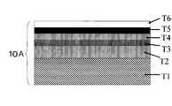
- FIG. 1 is a schematic cross-sectional view showing the configuration of a metal laminated substrate 5A for an oxide superconducting wire obtained by the production method of the present invention.
- a metal laminated substrate 5A for an oxide superconducting wire obtained by the production method of the present invention includes a nonmagnetic metal plate T1 and a metal foil T2 laminated on the nonmagnetic metal plate T1.
- the epitaxial growth film T3 is provided on the metal foil T2.
- the reason why the Ni film is formed on the epitaxial growth film T3 on the metal foil T2 is that the Ni film has better oxidation resistance than Cu (metal foil T2), and if there is no Ni layer on the Cu, such as CeO 2 This is because a Cu oxide film may be generated during the formation of the intermediate layer, and the orientation of the metal foil T2 may be lost.
- the nonmagnetic metal plate T1 preferably has a thickness of 0.05 mm or more and 0.2 mm or less. The reason why the thickness is 0.05 mm or more is to ensure the strength of the nonmagnetic metal plate T1, and the reason why the thickness is 0.2 mm or less is to ensure workability when processing the superconductor.
- the metal foil T2 is preferably made of Cu or a Cu alloy having a thickness of 7 ⁇ m or more and 50 ⁇ m or less that is cold-rolled at a rolling reduction of 90% or more (in the present specification, both may be referred to as a Cu alloy in some cases). If the rolling reduction is less than 90%, Cu may not be oriented in the heat treatment to be performed later.
- the reason why the thickness is 7 ⁇ m or more is to secure the strength of the metal foil T2, and the reason why the thickness is 50 ⁇ m or less is that using the metal foil T2. This is to ensure workability when processing the conductive material.
- the epitaxial growth film T3 is preferably made of Ni or Ni alloy having a thickness of 0.5 ⁇ m or more and 10 ⁇ m or less (in the present specification, both may be referred to as Ni alloy in some cases).
- the nonmagnetic metal plate T1 and the metal foil T2 are laminated by room temperature surface activation bonding, and after the lamination, the metal foil T2 is formed by heat treatment at 150 ° C. or more and 1000 ° C. or less. After the axial crystal orientation, an epitaxial growth film T3 is formed on the surface of the metal foil T2.
- non-magnetic means a state of 77K or higher and not a ferromagnet, that is, a Curie point or a Neel point existing at 77K or lower, and a temperature of 77K or higher is a paramagnetic or antiferromagnetic state.
- an austenitic stainless steel plate is preferably applied since it has a role as a reinforcing material having excellent strength.
- austenitic stainless steel is non-magnetic at normal temperature, that is, the metal structure is 100% austenite ( ⁇ ) phase, but the martensite ( ⁇ ′) phase transformation point (Ms point), which is a ferromagnetic material, is 77K or more. If it is located at ⁇ , the ⁇ ′ phase, which is a ferromagnetic substance, may develop at the liquid nitrogen temperature. For this reason, those designed to have an Ms point of 77K or lower are preferably used as the oxide superconducting wire used at a liquid nitrogen temperature (77K).
- the metal laminated substrate 5A for oxide superconducting wire is slit.
- the processed part is transformed into ⁇ ′ phase.
- the ⁇ -type stainless steel plate to be used has a stable ⁇ -phase designed to have an Ms point sufficiently lower than 77K, and is generally spread and can be obtained at a relatively low price such as SUS316 and SUS316L. desirable.
- a thickness of 20 ⁇ m or more is commercially available, but a thickness of 50 ⁇ m or more and 100 ⁇ m or less is desirable in consideration of foil thickness and strength of the oxide superconducting wire.
- an intermediate layer is formed on the surface and a superconductor layer is laminated thereon by epitaxial growth. Therefore, it is necessary to have a high degree of crystal orientation in the state of the laminated substrate. There is.
- Such a high-pressure under-rolled Cu alloy foil has been developed and popularized in order to have high flexibility in flexible mounting substrate applications, and has been easily available in the past few years.
- high pressure under-rolled Cu foil (HA foil (trade name)) manufactured by Nikko Materials Co., Ltd.
- high-pressure under-rolled Cu foil HX foil (trade name) manufactured by Hitachi Cable, Ltd.
- the commercially available high-pressure under-rolled Cu alloy foil as described above is preferably used because of its excellent crystal orientation.
- a thinner thickness is more economical, but a currently available one of 7 ⁇ m to 35 ⁇ m is desirable. More preferably, the thickness is 12 ⁇ m to 18 ⁇ m.
- the Cu alloy foil may be any additive element as long as it can be easily oriented to a (200) plane crystal orientation ratio of 99% or more by heat treatment, but Ag, Sn, Zn, Zr, O, N Is added in a small amount, and the total content is 1% or less.
- the reason why the total amount of the additive elements is 1% or less is that the additive element and Cu form a solid solution, but if the total content exceeds 1%, impurities such as oxides other than the solid material increase, and the orientation is increased. This is because there is a possibility that it will affect. Therefore, the total content is preferably 0.1% or less.
- the above-described austenitic stainless steel sheet and the Cu alloy foil cold-rolled at a reduction rate of 90% or more are bonded together by a surface activated bonding method.
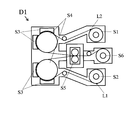
- An example of the surface activated bonding method is a vacuum surface activated bonding apparatus D1 shown in FIG.
- a nonmagnetic metal plate L1 and a Cu alloy foil L2 are prepared as long coils having a width of 150 mm to 600 mm, and are respectively installed in the recoiler parts S1 and S2 of the surface activated bonding apparatus D1.
- the non-magnetic metal plate L1 and the Cu alloy foil L2 conveyed from the recoiler parts S1 and S2 are continuously conveyed to the surface activation treatment step, and after the two surfaces to be joined are activated in advance, 0. Cold-weld at a rolling reduction of 1 to 5%.
- one electrode A non-magnetic metal plate L1 having a bonding surface and Cu alloy foil L2 each grounded in an extremely low pressure inert gas atmosphere of 10 to 1 ⁇ 10 ⁇ 2 Pa is grounded.
- an alternating current of 1 to 50 MHz is applied to another insulated and supported electrode B (S4) to generate a glow discharge, and the area of the electrode exposed in the plasma generated by the glow discharge is This is performed by performing sputter etching with 1/3 or less of the area of the electrode B.
- the inert gas argon, neon, xenon, krypton, or a mixed gas containing at least one of these can be used.
- the surface to be joined is sputtered with an inert gas to sputter the surface to which the nonmagnetic metal plate L1 and the Cu alloy foil L2 are joined, and the surface to be joined is activated.
- the electrode A (S3) takes the form of a cooling roll, preventing the temperature of each transport material from rising.
- the laminated body brought into close contact through the pressure welding process is transported to the winding process (S6) and wound there.
- heat treatment is performed in order to highly crystallize the high-pressure under-rolled Cu alloy foil.
- the heat treatment temperature needs to be 150 ° C. or higher in order to complete the recrystallization completely.
- the soaking time may be about 10 seconds in a continuous annealing furnace. If the heat treatment temperature is too high, the Cu foil or rolled Cu alloy foil tends to cause secondary recrystallization, and the crystal orientation deteriorates. Note that heat treatment at 600 ° C. to 900 ° C. is preferable in consideration of placing the substrate in a high temperature atmosphere of 600 ° C. to 900 ° C. in the intermediate layer deposition or superconductor layer deposition step.
- a high-strength and highly crystal-oriented nonmagnetic metal plate and Cu alloy foil metal laminate substrate is completed.
- a non-magnetic metal plate and a Cu alloy foil metal laminated substrate were obtained as follows.
- Table 1 shows the following measurement results when 200 ⁇ m wide 18 ⁇ m-thick high-pressure rolled Cu foil and 100 ⁇ m-thick SUS316L plate are bonded by a room temperature surface activation bonding method and then heat-treated at 200 ° C. to 1000 ° C. for 5 minutes.
- Crystal orientation ratio Ratio of Cu (200) plane parallel to Cu foil surface (2) Index value indicating that (200) plane is parallel to longitudinal direction ⁇ 001>
- crystal orientation The rate indicates the (200) plane intensity rate of the ⁇ / 2 ⁇ diffraction peak measured by X-ray diffraction, and the index value is ⁇ (°) as a biaxial orientation index (Ni (111) pole by X-ray diffraction).
- the peak intensity ratio when heat treatment is performed at 130 ° C. and 1050 ° C. is also shown.
- Table 1 also shows the peak strength ratio when a 30 ⁇ m-thick high-pressure rolled Ni foil is joined by the room temperature activated joining method and heat-treated at 1000 ° C. for 1 hour instead of Cu foil. .
- Table 1 shows the following.
- the crystal orientation rate is 93% when the heat treatment temperature is 130 ° C. ⁇ 5 minutes, which is still not sufficient, but in the range of 200 ° C. to 1000 ° C., the (200) plane crystal can be maintained for 5 minutes.
- the orientation rate is 99% or more.
- the temperature exceeds 1000 ° C. the uniaxial orientation of the (200) plane is destroyed by secondary recrystallization, and the strength ratio is reduced to 70%.
- the recrystallization temperature is in the vicinity of 700 ° C., and the strength rate is 98% even in heat treatment at 1000 ° C., which is considered to be optimal, and does not reach 99%, and ⁇ is 15.4 °.
- the crystal orientation degree that is, ⁇ indicating the biaxial orientation is 6 ° or less in any of the examples.
- This value is an average obtained by measuring a total of three points near both ends and the center of the plate in the width direction of 200 mm, and almost no difference was observed in the values.
- the highly crystal-oriented surface is a Cu alloy foil, and depending on the type of intermediate layer formed on this surface, there is a possibility that adhesion cannot be ensured due to Cu oxidation or the like.
- an Ni alloy is epitaxially formed on the Cu foil side surface of the metal laminated substrate.
- Cu and Ni are elements that are adjacent to each other in the periodic table of elements, the metal crystal structure is the same face-centered cubic crystal, and the lattice constants are close to each other.
- Ni alloy film forming method examples include various methods such as an electrolytic plating method, an electroless plating method, a vacuum deposition method, and a sputtering method. In consideration of continuous processing of a long coil particularly efficiently, film formation by an electrolytic plating method is preferable.
- the film thickness of the Ni alloy is to prevent Cu diffusion during the subsequent oxide intermediate layer film formation and superconductor layer film formation, and that Ni has magnetism, and that the crystal orientation is destroyed when the epitaxial growth exceeds 10 ⁇ m.
- the thickness is set to 0.5 ⁇ m or more and 10 ⁇ m or less. Preferably they are 0.5 micrometer or more and 3 micrometers or less.
- This Ni epitaxial growth film on the surface of highly crystallized Cu is improved from the crystal orientation of Ni obtained by conventional rolling and annealing ( ⁇ is about 8 °), and is equal to or higher than that of Ni—W alloy ( ⁇ ). ⁇ 7 °) High crystal orientation is obtained.
- the element contained in the Ni alloy to be formed one that can reduce magnetism is preferable.
- elements such as Cu, Sn, W, and Cr are listed.
- the surface roughness is preferably a mirror surface, but considering the current method and economy, it is desirable that Ra be 1 nm or more and 10 nm or less.
- a superior substrate can be obtained, and a high-performance oxide superconducting wire can be obtained.
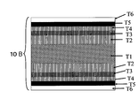
- FIG. 3 shows a metal laminated plate for an oxide superconducting wire obtained by the manufacturing method of another embodiment of the present invention, in which a Cu alloy foil T2 is bonded to both surfaces of a nonmagnetic metal plate T1 by surface activation bonding, and heat treatment is performed.
- FIG. 2 is a schematic cross-sectional view showing a configuration of an oxide superconducting wire 10A in which an intermediate layer T4, an oxide superconductor layer T5, and a protective film T6 are sequentially laminated on the metal laminated substrate 5A for oxide superconducting wire shown in FIG. It is.
- the oxide superconducting wire 10A is formed by epitaxially depositing an intermediate layer of CeO 2 , YSZ, SrTiO 3 , MgO or the like on a crystal-oriented epitaxial growth film T3 using a sputtering method or the like, and superconducting layers such as Y123 thin films are formed by laser. It is manufactured by forming a film by an abrasion method or the like and further laminating Ag, Cu or the like as a protective film on the superconductor layer.
- FIG. 4 is a schematic cross-sectional view showing a configuration of an oxide superconducting wire 10B showing another embodiment of the oxide superconducting wire of the present invention.
- the metal laminated substrate for oxide superconducting wire has a high degree of crystal orientation, the intermediate layer and the superconductor layer can be easily epitaxially grown, and has high superconducting properties under a liquid nitrogen temperature of 77 K, that is, a high critical current density. Superconducting wire can be made.
- the metal laminated substrate for oxide superconducting wire has high strength, it is easy to handle in the intermediate layer and superconductor layer forming step.
- the metal multilayer substrate for oxide superconducting wire has almost no magnetism and can be used for AC applications that are difficult with Ni—W alloys. d. Since the metal laminated substrate for oxide superconducting wire can produce wide and long coils, the production of oxide superconducting wire with wide and long coils, slitting in the final process, and finishing into wires makes the productivity Can be made more efficient.
- Table 2 shows the following.
- the Ni plating layer was epitaxially grown on the highly (200) crystal-oriented Cu foil surface of the base, and had the same value as the Cu foil surface. Even when the Ni thickness was increased to 3 ⁇ m (Example 1-3), the crystal orientation was not changed.
- a comparative example Comparative Example 1-1
- An intermediate layer (CeO 2 / YSZ / CeO 2 ) and an oxide superconductor layer (RE (1) Ba (2) Cu are formed on various metal laminated substrate tapes for oxide superconducting wires manufactured by the manufacturing method of the present invention.
- (3) After depositing 1.2 ⁇ m of O (7 ⁇ ); RE Y, Gd, Ho, etc.), an Ag protective film was formed to complete the superconducting wire.
- Table 3 shows the results of measuring the superconductor characteristics of the oxide superconducting wire obtained in Example 2 at a length of 15 cm and the hysteresis due to saturation magnetization, which is an index of AC loss in the state in which the intermediate layer is formed. .
- Table 3 shows the following. All the oxide superconducting wires of Example 2 showed high strength of 480 MPa or more. In the critical current density below 77K, which is a superconducting characteristic, all showed a value of 1 MA / cm 2 or more. Also, the hysteresis was 1/26 or less when the Ni plating thickness was 1 ⁇ m, compared with the Ni-5% W alloy shown in the comparative example. In Example 2-1, the value is smaller than this value. In Example 2-5, this value is slightly larger than this value, but it is a sufficiently usable value.
- the oxide superconducting wire of the present invention has a variety of characteristics impossible with conventional substrates, i.e., substrate strength, non-magnetic properties, and a high degree of crystal orientation, in a well-balanced manner, and a commercially available material can be used. Manufacturing of a long and wide coil can be realized, which has the effect of reducing cost and improving mass productivity.
- the production method of the present invention is industrially useful as a method for producing a metal laminated substrate for oxide superconducting wire and an oxide superconducting wire using the same.
- T1 non-magnetic metal plate T2 Cu alloy foil, Epitaxial growth film of T3 Ni alloy, T4 middle layer, T5 oxide superconductor layer, T6 protective film, 5A, 5B metal laminated substrate, 10A, 10B Oxide superconducting wire.
Landscapes
- Engineering & Computer Science (AREA)
- Manufacturing & Machinery (AREA)
- Superconductors And Manufacturing Methods Therefor (AREA)
Priority Applications (4)
| Application Number | Priority Date | Filing Date | Title |
|---|---|---|---|
| EP09825905.4A EP2357656B1 (en) | 2008-11-12 | 2009-11-11 | Method for producing a metal laminated substrate for an oxide superconducting wire, and oxide superconducting wire using the substrate |
| KR1020117010376A KR101258439B1 (ko) | 2008-11-12 | 2009-11-11 | 산화물 초전도 선재용 금속 적층 기판의 제조 방법 및 당해 기판을 이용한 산화물 초전도 선재 |
| CN2009801447838A CN102209995B (zh) | 2008-11-12 | 2009-11-11 | 氧化物超导线材用金属叠层衬底的制造方法及使用该衬底的氧化物超导线材 |
| US13/127,928 US9034124B2 (en) | 2008-11-12 | 2009-11-11 | Method for producing metal laminated substrate for oxide superconducting wire, and oxide superconducting wire using the substrate |
Applications Claiming Priority (2)
| Application Number | Priority Date | Filing Date | Title |
|---|---|---|---|
| JP2008-290308 | 2008-11-12 | ||
| JP2008290308A JP5382911B2 (ja) | 2008-11-12 | 2008-11-12 | 酸化物超電導線材用金属積層基板の製造方法及び該基板を用いた酸化物超電導線材 |
Publications (1)
| Publication Number | Publication Date |
|---|---|
| WO2010055651A1 true WO2010055651A1 (ja) | 2010-05-20 |
Family
ID=42169796
Family Applications (1)
| Application Number | Title | Priority Date | Filing Date |
|---|---|---|---|
| PCT/JP2009/006018 Ceased WO2010055651A1 (ja) | 2008-11-12 | 2009-11-11 | 酸化物超電導線材用金属積層基板の製造方法及び該基板を用いた酸化物超電導線材 |
Country Status (6)
| Country | Link |
|---|---|
| US (1) | US9034124B2 (enExample) |
| EP (1) | EP2357656B1 (enExample) |
| JP (1) | JP5382911B2 (enExample) |
| KR (1) | KR101258439B1 (enExample) |
| CN (1) | CN102209995B (enExample) |
| WO (1) | WO2010055651A1 (enExample) |
Cited By (6)
| Publication number | Priority date | Publication date | Assignee | Title |
|---|---|---|---|---|
| JP2010129432A (ja) * | 2008-11-28 | 2010-06-10 | Sumitomo Electric Ind Ltd | 前駆体の製造方法、超電導線材の製造方法、前駆体および超電導線材 |
| JP2012216487A (ja) * | 2011-03-31 | 2012-11-08 | Korea Electrotechnology Research Inst | 高温超伝導線材 |
| US20140008634A1 (en) * | 2011-04-05 | 2014-01-09 | Mitsui Mining & Smelting Co., Ltd. | Electrode Sheet for Organic Device, Organic Device Module, and Method for Producing Same |
| US20150001519A1 (en) * | 2012-02-07 | 2015-01-01 | Mitsui Mining & Smelting Co., Ltd. | Electrode Foil and Electronic Device |
| WO2017064893A1 (ja) * | 2015-10-15 | 2017-04-20 | 住友電気工業株式会社 | 酸化物超電導線材 |
| EP2503560A4 (en) * | 2009-11-20 | 2017-12-20 | Toyo Kohan Co., Ltd. | Substrate for superconducting compound and method for manufacturing the substrate |
Families Citing this family (20)
| Publication number | Priority date | Publication date | Assignee | Title |
|---|---|---|---|---|
| IN2012DN00632A (enExample) * | 2009-07-17 | 2015-08-21 | Toyo Kohan Co Ltd | |
| JP2012119125A (ja) * | 2010-11-30 | 2012-06-21 | Sumitomo Electric Ind Ltd | 薄膜超電導線材用金属基材とその製造方法および薄膜超電導線材 |
| JP5904869B2 (ja) * | 2012-05-11 | 2016-04-20 | Jx金属株式会社 | 超電導膜形成用圧延銅箔の製造方法 |
| WO2014054351A1 (ja) | 2012-10-05 | 2014-04-10 | 東洋鋼鈑株式会社 | エピタキシャル成長用基板及びその製造方法、並びに超電導線材用基板 |
| US9825209B2 (en) * | 2012-12-21 | 2017-11-21 | Panasonic Intellectual Property Management Co., Ltd. | Electronic component package and method for manufacturing the same |
| JP5624696B1 (ja) | 2012-12-21 | 2014-11-12 | パナソニック株式会社 | 電子部品パッケージおよびその製造方法 |
| CN104603932A (zh) | 2012-12-21 | 2015-05-06 | 松下知识产权经营株式会社 | 电子部件封装件及其制造方法 |
| WO2014097643A1 (ja) | 2012-12-21 | 2014-06-26 | パナソニック株式会社 | 電子部品パッケージおよびその製造方法 |
| JP6244142B2 (ja) | 2013-09-04 | 2017-12-06 | 東洋鋼鈑株式会社 | 超電導線材用基板及びその製造方法、並びに超電導線材 |
| US10229777B2 (en) | 2013-10-31 | 2019-03-12 | General Electric Company | Graded magnetic component and method of forming |
| US10229776B2 (en) | 2013-10-31 | 2019-03-12 | General Electric Company | Multi-phase magnetic component and method of forming |
| KR101631859B1 (ko) * | 2014-08-12 | 2016-06-20 | 한국전기연구원 | 적층 고온초전도 선재 및 그 제조방법 |
| TWI632726B (zh) * | 2014-10-21 | 2018-08-11 | 加川清二 | 微多孔金屬箔的製造方法及裝置 |
| KR102403087B1 (ko) * | 2014-10-27 | 2022-05-27 | 도요 고한 가부시키가이샤 | 초전도 선재용 기판 및 그 제조 방법과 초전도 선재 |
| CN104851513B (zh) * | 2015-05-15 | 2017-08-08 | 富通集团(天津)超导技术应用有限公司 | 一种超导线材及其制备方法 |
| CN104953022A (zh) * | 2015-05-15 | 2015-09-30 | 富通集团(天津)超导技术应用有限公司 | 超导线材的制备方法 |
| KR102314493B1 (ko) * | 2017-07-13 | 2021-10-18 | 한국전기연구원 | 표면이 가공된 초전도선재 및 그 제조방법 |
| CN111613383B (zh) * | 2020-06-16 | 2021-12-21 | 深圳供电局有限公司 | 一种提高热稳定性的高温超导带材 |
| US11926880B2 (en) | 2021-04-21 | 2024-03-12 | General Electric Company | Fabrication method for a component having magnetic and non-magnetic dual phases |
| US11661646B2 (en) | 2021-04-21 | 2023-05-30 | General Electric Comapny | Dual phase magnetic material component and method of its formation |
Citations (8)
| Publication number | Priority date | Publication date | Assignee | Title |
|---|---|---|---|---|
| JP2001110255A (ja) | 1999-10-07 | 2001-04-20 | Furukawa Electric Co Ltd:The | 高強度配向多結晶金属基板および酸化物超電導線材 |
| WO2004088677A1 (ja) | 2003-03-31 | 2004-10-14 | The Furukawa Electric Co., Ltd. | 酸化物超電導線材用金属基板、酸化物超電導線材及びその製造方法 |
| JP3587956B2 (ja) | 1997-06-10 | 2004-11-10 | 古河電気工業株式会社 | 酸化物超電導線材およびその製造方法 |
| JP3601830B2 (ja) | 1995-04-10 | 2004-12-15 | ユーティ―バテル エルエルシー | 効果的な2軸配向組織を有する構造体及び同構造体の製造方法 |
| JP2006127847A (ja) * | 2004-10-27 | 2006-05-18 | Sumitomo Electric Ind Ltd | 膜形成用配向基板および超電導線材 |
| JP2006286212A (ja) | 2005-03-31 | 2006-10-19 | Furukawa Electric Co Ltd:The | 酸化物超電導用高強度多結晶金属基板とそれを用いた酸化物超電導線材 |
| JP2007200831A (ja) | 2005-12-26 | 2007-08-09 | Furukawa Electric Co Ltd:The | 超電導体用基材およびその製造方法 |
| JP2008210600A (ja) * | 2007-02-26 | 2008-09-11 | Internatl Superconductivity Technology Center | 希土類系テープ状酸化物超電導体及びそれに用いる複合基板 |
Family Cites Families (12)
| Publication number | Priority date | Publication date | Assignee | Title |
|---|---|---|---|---|
| US3601830A (en) | 1968-10-24 | 1971-08-31 | Jordan H Stover | Self-locking bolt and manufacture thereof |
| US3587956A (en) | 1969-05-02 | 1971-06-28 | Libbey Ownens Ford Co | Apparatus for cutting glass plates |
| JPS6026619A (ja) * | 1983-07-22 | 1985-02-09 | Nippon Kokan Kk <Nkk> | オ−ステナイト系ステンレス厚鋼板の製造方法 |
| DE3545182A1 (de) * | 1985-12-20 | 1987-06-25 | Krupp Gmbh | Austenitischer, stickstoffhaltiger crnimomn-stahl, verfahren zu seiner herstellung und seine verwendung |
| CN1045483A (zh) * | 1989-03-09 | 1990-09-19 | 日本钢管株式会社 | 超导体制件 |
| ATE353375T1 (de) * | 2000-12-07 | 2007-02-15 | Leibniz Inst Fuer Festkoerper | Metallband für epitaktische beschichtungen und verfahren zu dessen herstellung |
| US6743531B2 (en) * | 2001-06-22 | 2004-06-01 | Fujikura Ltd. | Oxide superconducting conductor and its production method |
| JP2003193211A (ja) * | 2001-12-27 | 2003-07-09 | Nippon Mining & Metals Co Ltd | 銅張積層板用圧延銅箔 |
| US6642092B1 (en) * | 2002-07-11 | 2003-11-04 | Sharp Laboratories Of America, Inc. | Thin-film transistors formed on a metal foil substrate |
| JP3979647B2 (ja) * | 2003-02-14 | 2007-09-19 | 東洋鋼鈑株式会社 | 合金層積層体の製造方法および合金層積層体を用いた部品の製造方法 |
| CN2681295Y (zh) * | 2003-12-15 | 2005-02-23 | 北京有色金属研究总院 | 多层双轴取向隔离层结构 |
| JP5074083B2 (ja) * | 2007-04-17 | 2012-11-14 | 中部電力株式会社 | エピタキシャル薄膜形成用のクラッド配向金属基板及びその製造方法 |
-
2008
- 2008-11-12 JP JP2008290308A patent/JP5382911B2/ja not_active Expired - Fee Related
-
2009
- 2009-11-11 US US13/127,928 patent/US9034124B2/en active Active
- 2009-11-11 WO PCT/JP2009/006018 patent/WO2010055651A1/ja not_active Ceased
- 2009-11-11 CN CN2009801447838A patent/CN102209995B/zh not_active Expired - Fee Related
- 2009-11-11 EP EP09825905.4A patent/EP2357656B1/en not_active Not-in-force
- 2009-11-11 KR KR1020117010376A patent/KR101258439B1/ko active Active
Patent Citations (8)
| Publication number | Priority date | Publication date | Assignee | Title |
|---|---|---|---|---|
| JP3601830B2 (ja) | 1995-04-10 | 2004-12-15 | ユーティ―バテル エルエルシー | 効果的な2軸配向組織を有する構造体及び同構造体の製造方法 |
| JP3587956B2 (ja) | 1997-06-10 | 2004-11-10 | 古河電気工業株式会社 | 酸化物超電導線材およびその製造方法 |
| JP2001110255A (ja) | 1999-10-07 | 2001-04-20 | Furukawa Electric Co Ltd:The | 高強度配向多結晶金属基板および酸化物超電導線材 |
| WO2004088677A1 (ja) | 2003-03-31 | 2004-10-14 | The Furukawa Electric Co., Ltd. | 酸化物超電導線材用金属基板、酸化物超電導線材及びその製造方法 |
| JP2006127847A (ja) * | 2004-10-27 | 2006-05-18 | Sumitomo Electric Ind Ltd | 膜形成用配向基板および超電導線材 |
| JP2006286212A (ja) | 2005-03-31 | 2006-10-19 | Furukawa Electric Co Ltd:The | 酸化物超電導用高強度多結晶金属基板とそれを用いた酸化物超電導線材 |
| JP2007200831A (ja) | 2005-12-26 | 2007-08-09 | Furukawa Electric Co Ltd:The | 超電導体用基材およびその製造方法 |
| JP2008210600A (ja) * | 2007-02-26 | 2008-09-11 | Internatl Superconductivity Technology Center | 希土類系テープ状酸化物超電導体及びそれに用いる複合基板 |
Non-Patent Citations (2)
| Title |
|---|
| D.P. NORTON ET AL., SCIENCE, vol. 274, 1996, pages 755 |
| See also references of EP2357656A4 |
Cited By (10)
| Publication number | Priority date | Publication date | Assignee | Title |
|---|---|---|---|---|
| JP2010129432A (ja) * | 2008-11-28 | 2010-06-10 | Sumitomo Electric Ind Ltd | 前駆体の製造方法、超電導線材の製造方法、前駆体および超電導線材 |
| US8865627B2 (en) | 2008-11-28 | 2014-10-21 | Sumitomo Electric Industries, Ltd. | Method for manufacturing precursor, method for manufacturing superconducting wire, precursor, and superconducting wire |
| US9570215B2 (en) | 2008-11-28 | 2017-02-14 | Sumitomo Electric Industries, Ltd. | Method for manufacturing precursor, method for manufacturing superconducting wire, precursor, and superconducting wire |
| EP2503560A4 (en) * | 2009-11-20 | 2017-12-20 | Toyo Kohan Co., Ltd. | Substrate for superconducting compound and method for manufacturing the substrate |
| JP2012216487A (ja) * | 2011-03-31 | 2012-11-08 | Korea Electrotechnology Research Inst | 高温超伝導線材 |
| EP2506324A3 (en) * | 2011-03-31 | 2014-01-15 | Korea Electrotechnology Research Institute | High-temperature superconducting tape |
| US20140008634A1 (en) * | 2011-04-05 | 2014-01-09 | Mitsui Mining & Smelting Co., Ltd. | Electrode Sheet for Organic Device, Organic Device Module, and Method for Producing Same |
| US20150001519A1 (en) * | 2012-02-07 | 2015-01-01 | Mitsui Mining & Smelting Co., Ltd. | Electrode Foil and Electronic Device |
| WO2017064893A1 (ja) * | 2015-10-15 | 2017-04-20 | 住友電気工業株式会社 | 酸化物超電導線材 |
| US10665367B2 (en) | 2015-10-15 | 2020-05-26 | Sumitomo Electric Industries, Ltd. | Oxide superconducting wire |
Also Published As
| Publication number | Publication date |
|---|---|
| EP2357656B1 (en) | 2016-06-08 |
| US9034124B2 (en) | 2015-05-19 |
| CN102209995B (zh) | 2013-10-09 |
| US20120040840A1 (en) | 2012-02-16 |
| JP2010118246A (ja) | 2010-05-27 |
| KR101258439B1 (ko) | 2013-04-26 |
| EP2357656A4 (en) | 2014-05-07 |
| CN102209995A (zh) | 2011-10-05 |
| EP2357656A1 (en) | 2011-08-17 |
| JP5382911B2 (ja) | 2014-01-08 |
| KR20110082551A (ko) | 2011-07-19 |
Similar Documents
| Publication | Publication Date | Title |
|---|---|---|
| JP5382911B2 (ja) | 酸化物超電導線材用金属積層基板の製造方法及び該基板を用いた酸化物超電導線材 | |
| JP5723773B2 (ja) | 酸化物超電導線材用金属積層基板の製造方法 | |
| JP5828014B2 (ja) | 半導体素子形成用金属積層基板の製造方法及び半導体素子形成用金属積層基板 | |
| JP4268645B2 (ja) | 希土類系テープ状酸化物超電導体及びそれに用いる複合基板 | |
| KR102403087B1 (ko) | 초전도 선재용 기판 및 그 제조 방법과 초전도 선재 | |
| JP6244142B2 (ja) | 超電導線材用基板及びその製造方法、並びに超電導線材 | |
| JP6250546B2 (ja) | エピタキシャル成長用基板及びその製造方法、並びに超電導線材用基板 | |
| JP6074527B2 (ja) | エピタキシャル成長用基板及びその製造方法、並びに超電導線材用基板 | |
| JP5323444B2 (ja) | 酸化物超電導線材用複合基板、その製造方法、及び超電導線材 | |
| JP6948621B2 (ja) | エピタキシャル成長用基板及びその製造方法 | |
| JP2013101832A (ja) | エピタキシャル成長用基板及びその製造方法、並びに超電導線材用基板 | |
| CN105518808B (zh) | 超导线材用基板及其制造方法、以及超导线材 |
Legal Events
| Date | Code | Title | Description |
|---|---|---|---|
| WWE | Wipo information: entry into national phase |
Ref document number: 200980144783.8 Country of ref document: CN |
|
| 121 | Ep: the epo has been informed by wipo that ep was designated in this application |
Ref document number: 09825905 Country of ref document: EP Kind code of ref document: A1 |
|
| ENP | Entry into the national phase |
Ref document number: 20117010376 Country of ref document: KR Kind code of ref document: A |
|
| NENP | Non-entry into the national phase |
Ref country code: DE |
|
| WWE | Wipo information: entry into national phase |
Ref document number: 2009825905 Country of ref document: EP |
|
| WWE | Wipo information: entry into national phase |
Ref document number: 13127928 Country of ref document: US |