WO2010038452A1 - リードフレーム基板とその製造方法、及び半導体装置 - Google Patents
リードフレーム基板とその製造方法、及び半導体装置 Download PDFInfo
- Publication number
- WO2010038452A1 WO2010038452A1 PCT/JP2009/005041 JP2009005041W WO2010038452A1 WO 2010038452 A1 WO2010038452 A1 WO 2010038452A1 JP 2009005041 W JP2009005041 W JP 2009005041W WO 2010038452 A1 WO2010038452 A1 WO 2010038452A1
- Authority
- WO
- WIPO (PCT)
- Prior art keywords
- semiconductor element
- connection terminal
- outer frame
- lead frame
- external connection
- Prior art date
- Legal status (The legal status is an assumption and is not a legal conclusion. Google has not performed a legal analysis and makes no representation as to the accuracy of the status listed.)
- Ceased
Links
Images







Classifications
-
- H—ELECTRICITY
- H10—SEMICONDUCTOR DEVICES; ELECTRIC SOLID-STATE DEVICES NOT OTHERWISE PROVIDED FOR
- H10W—GENERIC PACKAGES, INTERCONNECTIONS, CONNECTORS OR OTHER CONSTRUCTIONAL DETAILS OF DEVICES COVERED BY CLASS H10
- H10W70/00—Package substrates; Interposers; Redistribution layers [RDL]
- H10W70/01—Manufacture or treatment
- H10W70/04—Manufacture or treatment of leadframes
- H10W70/042—Etching
-
- H—ELECTRICITY
- H10—SEMICONDUCTOR DEVICES; ELECTRIC SOLID-STATE DEVICES NOT OTHERWISE PROVIDED FOR
- H10W—GENERIC PACKAGES, INTERCONNECTIONS, CONNECTORS OR OTHER CONSTRUCTIONAL DETAILS OF DEVICES COVERED BY CLASS H10
- H10W72/00—Interconnections or connectors in packages
-
- H—ELECTRICITY
- H10—SEMICONDUCTOR DEVICES; ELECTRIC SOLID-STATE DEVICES NOT OTHERWISE PROVIDED FOR
- H10W—GENERIC PACKAGES, INTERCONNECTIONS, CONNECTORS OR OTHER CONSTRUCTIONAL DETAILS OF DEVICES COVERED BY CLASS H10
- H10W70/00—Package substrates; Interposers; Redistribution layers [RDL]
- H10W70/40—Leadframes
-
- H—ELECTRICITY
- H10—SEMICONDUCTOR DEVICES; ELECTRIC SOLID-STATE DEVICES NOT OTHERWISE PROVIDED FOR
- H10W—GENERIC PACKAGES, INTERCONNECTIONS, CONNECTORS OR OTHER CONSTRUCTIONAL DETAILS OF DEVICES COVERED BY CLASS H10
- H10W70/00—Package substrates; Interposers; Redistribution layers [RDL]
- H10W70/40—Leadframes
- H10W70/421—Shapes or dispositions
-
- H—ELECTRICITY
- H10—SEMICONDUCTOR DEVICES; ELECTRIC SOLID-STATE DEVICES NOT OTHERWISE PROVIDED FOR
- H10W—GENERIC PACKAGES, INTERCONNECTIONS, CONNECTORS OR OTHER CONSTRUCTIONAL DETAILS OF DEVICES COVERED BY CLASS H10
- H10W70/00—Package substrates; Interposers; Redistribution layers [RDL]
- H10W70/60—Insulating or insulated package substrates; Interposers; Redistribution layers
- H10W70/62—Insulating or insulated package substrates; Interposers; Redistribution layers characterised by their interconnections
- H10W70/65—Shapes or dispositions of interconnections
- H10W70/654—Top-view layouts
- H10W70/656—Fan-in layouts
-
- H—ELECTRICITY
- H10—SEMICONDUCTOR DEVICES; ELECTRIC SOLID-STATE DEVICES NOT OTHERWISE PROVIDED FOR
- H10W—GENERIC PACKAGES, INTERCONNECTIONS, CONNECTORS OR OTHER CONSTRUCTIONAL DETAILS OF DEVICES COVERED BY CLASS H10
- H10W72/00—Interconnections or connectors in packages
- H10W72/071—Connecting or disconnecting
- H10W72/073—Connecting or disconnecting of die-attach connectors
- H10W72/07351—Connecting or disconnecting of die-attach connectors characterised by changes in properties of the die-attach connectors during connecting
- H10W72/07353—Connecting or disconnecting of die-attach connectors characterised by changes in properties of the die-attach connectors during connecting changes in shapes
-
- H—ELECTRICITY
- H10—SEMICONDUCTOR DEVICES; ELECTRIC SOLID-STATE DEVICES NOT OTHERWISE PROVIDED FOR
- H10W—GENERIC PACKAGES, INTERCONNECTIONS, CONNECTORS OR OTHER CONSTRUCTIONAL DETAILS OF DEVICES COVERED BY CLASS H10
- H10W72/00—Interconnections or connectors in packages
- H10W72/30—Die-attach connectors
- H10W72/331—Shapes of die-attach connectors
- H10W72/334—Cross-sectional shape, i.e. in side view
-
- H—ELECTRICITY
- H10—SEMICONDUCTOR DEVICES; ELECTRIC SOLID-STATE DEVICES NOT OTHERWISE PROVIDED FOR
- H10W—GENERIC PACKAGES, INTERCONNECTIONS, CONNECTORS OR OTHER CONSTRUCTIONAL DETAILS OF DEVICES COVERED BY CLASS H10
- H10W72/00—Interconnections or connectors in packages
- H10W72/50—Bond wires
- H10W72/551—Materials of bond wires
- H10W72/552—Materials of bond wires comprising metals or metalloids, e.g. silver
- H10W72/5522—Materials of bond wires comprising metals or metalloids, e.g. silver comprising gold [Au]
-
- H—ELECTRICITY
- H10—SEMICONDUCTOR DEVICES; ELECTRIC SOLID-STATE DEVICES NOT OTHERWISE PROVIDED FOR
- H10W—GENERIC PACKAGES, INTERCONNECTIONS, CONNECTORS OR OTHER CONSTRUCTIONAL DETAILS OF DEVICES COVERED BY CLASS H10
- H10W72/00—Interconnections or connectors in packages
- H10W72/851—Dispositions of multiple connectors or interconnections
- H10W72/874—On different surfaces
- H10W72/884—Die-attach connectors and bond wires
-
- H—ELECTRICITY
- H10—SEMICONDUCTOR DEVICES; ELECTRIC SOLID-STATE DEVICES NOT OTHERWISE PROVIDED FOR
- H10W—GENERIC PACKAGES, INTERCONNECTIONS, CONNECTORS OR OTHER CONSTRUCTIONAL DETAILS OF DEVICES COVERED BY CLASS H10
- H10W72/00—Interconnections or connectors in packages
- H10W72/90—Bond pads, in general
- H10W72/931—Shapes of bond pads
-
- H—ELECTRICITY
- H10—SEMICONDUCTOR DEVICES; ELECTRIC SOLID-STATE DEVICES NOT OTHERWISE PROVIDED FOR
- H10W—GENERIC PACKAGES, INTERCONNECTIONS, CONNECTORS OR OTHER CONSTRUCTIONAL DETAILS OF DEVICES COVERED BY CLASS H10
- H10W74/00—Encapsulations, e.g. protective coatings
-
- H—ELECTRICITY
- H10—SEMICONDUCTOR DEVICES; ELECTRIC SOLID-STATE DEVICES NOT OTHERWISE PROVIDED FOR
- H10W—GENERIC PACKAGES, INTERCONNECTIONS, CONNECTORS OR OTHER CONSTRUCTIONAL DETAILS OF DEVICES COVERED BY CLASS H10
- H10W74/00—Encapsulations, e.g. protective coatings
- H10W74/10—Encapsulations, e.g. protective coatings characterised by their shape or disposition
- H10W74/111—Encapsulations, e.g. protective coatings characterised by their shape or disposition the semiconductor body being completely enclosed
-
- H—ELECTRICITY
- H10—SEMICONDUCTOR DEVICES; ELECTRIC SOLID-STATE DEVICES NOT OTHERWISE PROVIDED FOR
- H10W—GENERIC PACKAGES, INTERCONNECTIONS, CONNECTORS OR OTHER CONSTRUCTIONAL DETAILS OF DEVICES COVERED BY CLASS H10
- H10W90/00—Package configurations
- H10W90/701—Package configurations characterised by the relative positions of pads or connectors relative to package parts
- H10W90/731—Package configurations characterised by the relative positions of pads or connectors relative to package parts of die-attach connectors
- H10W90/736—Package configurations characterised by the relative positions of pads or connectors relative to package parts of die-attach connectors between a chip and a stacked lead frame, conducting package substrate or heat sink
-
- H—ELECTRICITY
- H10—SEMICONDUCTOR DEVICES; ELECTRIC SOLID-STATE DEVICES NOT OTHERWISE PROVIDED FOR
- H10W—GENERIC PACKAGES, INTERCONNECTIONS, CONNECTORS OR OTHER CONSTRUCTIONAL DETAILS OF DEVICES COVERED BY CLASS H10
- H10W90/00—Package configurations
- H10W90/701—Package configurations characterised by the relative positions of pads or connectors relative to package parts
- H10W90/751—Package configurations characterised by the relative positions of pads or connectors relative to package parts of bond wires
- H10W90/756—Package configurations characterised by the relative positions of pads or connectors relative to package parts of bond wires between a chip and a stacked lead frame, conducting package substrate or heat sink
Definitions
- the present invention relates to a semiconductor package substrate and a semiconductor device suitable for mounting a semiconductor element, and more particularly to a lead frame substrate, a manufacturing method thereof, and a semiconductor device using them.
- outer leads for connection to a printed wiring board are arranged on the side surface of the semiconductor package.
- the lead frame forms a desired photoresist pattern on both sides of the metal plate, and etches from both sides, thereby fixing the semiconductor element mounting part, the inner lead and outer leads that are the connection parts with the semiconductor element electrode, and these.
- An outer frame part can be obtained. Moreover, it can obtain also by the punching process by a press other than an etching construction method.
- the electrode of the semiconductor element and the inner lead are electrically connected using a gold wire or the like. Thereafter, the vicinity of the semiconductor element including the inner lead portion is sealed with resin, the outer frame portion is cut, and the outer lead is bent as necessary.
- the outer leads placed on the side surfaces in this way are limited to 200 to 300 pins in a package size of about 30 mm square in view of the processing capability for miniaturization.
- the number of electrodes of a semiconductor element gradually increases, the number of terminals can no longer be accommodated in a lead frame type semiconductor package having outer leads on the side surfaces.
- the external connection terminal with a printed wiring board such as a grid array) type has been replaced with a semiconductor package arranged in an array on the bottom surface of the package board.
- the board used for these is drilled in a double-sided copper-coated glass epoxy board with a drill, the inside of the hole is made conductive by plating, one side is a terminal for connecting to the electrode of the semiconductor element, the other side It is common to form external connection terminals arranged in an array.
- the manufacture of these substrates is complicated and expensive, and has a problem that the reliability is inferior to that of a lead frame type package because plating is used for wiring connection in the substrate. is there.
- Patent Document 1 a BGA type semiconductor package structure using a lead frame using a process of etching the lead frame from both sides is disclosed.
- connection terminals for the semiconductor element electrodes are formed on the surface, and the external connection terminals are formed in an array on the other surface.
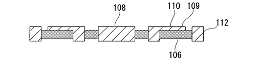
- FIGS. 5A and 5B A cross-sectional view of a prior art lead frame substrate is shown in FIGS. 5A and 5B.
- the length of the wiring 110 on the semiconductor element electrode connection terminal 109 side becomes longer.
- This wiring is produced by half-etching a metal plate. The width and thickness of the wiring are small, and there is a problem that the yield is very poor due to the occurrence of bending or bending in the steps after the etching.
- FIG. 6C shows the state of the resin layer in the vicinity of the external connection terminal that has been heat-cured after printing. As schematically shown in FIGS. 6A to 6C, there is a concern that bubbles are formed beyond the external connection terminal in the printing direction (indicated by arrow D1).
- the present invention has been invented in view of such problems of the prior art, can cope well with an increase in the number of electrodes of a semiconductor element, does not contain bubbles, has high reliability, and is manufactured and has a semiconductor package. It is an object of the present invention to provide a lead frame substrate that can be stably assembled, a method for manufacturing the same, and a related semiconductor device.
- a metal plate having a first surface and a second surface, a semiconductor element mounting portion, a semiconductor element electrode connection terminal, and a first element formed on the first surface.
- the lead frame substrate is characterized in that at least one protrusion is formed on the side bottom of the first surface.
- a semiconductor element mounting portion, a semiconductor element electrode connection terminal, and an outer frame portion are formed on the first surface of the metal plate, and the semiconductor plate is formed on the second surface of the metal plate.
- a photoresist pattern for forming an external connection terminal connected to the device electrode connection terminal and an outer frame portion is formed, and the photoresist pattern for forming the external connection terminal has a protruding shape at one or more places.
- a hole not penetrating is formed in the exposed portion of the metal plate where the metal plate of the second surface is exposed by etching, and the direction of the protruding portion from the external connection terminal is formed in the hole.
- a liquid pre-mold resin is applied to the resin, a resin layer is formed by heat curing, and the first surface is etched to be electrically connected to the semiconductor element mounting portion and the external connection terminal.
- a manufacturing method of a lead frame substrate, and forming a semiconductor element electrode connecting terminal, and an outer frame portion is a manufacturing method of a lead frame substrate, and forming a semiconductor element electrode connecting terminal, and an outer frame portion.
- a metal plate having a first surface and a second surface, a semiconductor element mounting portion, a semiconductor element electrode connection terminal, and a first element formed on the first surface.
- a lead frame substrate having at least one projecting portion formed on a side bottom of the first surface; a semiconductor element mounted on the lead frame substrate; and the lead frame substrate and the semiconductor by wire bonding
- the electrical connection with the device is made,
- a semiconductor device comprising.
- external connection terminals for connecting to a printed wiring board can be arranged in an array on the entire back surface of the lead frame substrate, which can cope with an increase in the number of terminals of semiconductor elements. Moreover, since it is a board
- FIG. 3B is a cross-sectional view in the next step of FIG. 1B, illustrating an example of the method for manufacturing the lead frame substrate according to the embodiment of the present invention.
- FIG. 3A is a cross-sectional view in the next step of FIG. 1C, showing an example of the method for manufacturing the lead frame substrate of the embodiment of the present invention.
- FIG. 2C is a cross-sectional view in the next step of FIG. 1D, showing an example of the method for manufacturing the lead frame substrate of the embodiment of the present invention.
- FIG. 1B is a cross-sectional view in the next step of FIG. 1B, illustrating an example of the method for manufacturing the lead frame substrate according to the embodiment of the present invention.
- FIG. 3A is a cross-sectional view in the next step of FIG. 1C, showing an example of the method for manufacturing the lead frame substrate of the embodiment of the present invention.
- FIG. 2C is a cross-sectional view in the next step of FIG. 1D, showing an example of the method for manufacturing
- FIG. 8B is a cross-sectional view in the next step of FIG. 1E, illustrating an example of the method for manufacturing the lead frame substrate according to the embodiment of the present invention. It is a top view which shows the photoresist pattern in the lead frame board
- FIGS. 1A to 1F A schematic cross section of the manufacturing process of the lead frame substrate is shown in FIGS. 1A to 1F.
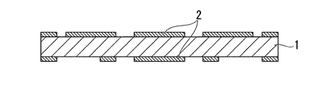
- Photoresist patterns 2 are formed on both surfaces of the metal plate 1 used for the lead frame (FIG. 1B). 1A to 1F, the pattern of the semiconductor element mounting portion 8, the connection terminal 9 to the semiconductor element electrode, the wiring 10, and the outer frame portion 12 is formed on the upper surface, and the pattern of the external connection terminal 11 and the outer frame portion is formed on the lower surface. To do.
- one or more protrusions 13 are appropriately formed.
- the pattern of the protrusion 13 made of this photoresist is designed so that the second metal surface does not remain by subsequent etching.
- the pattern of the protrusions 13 is generally good to set the width to 30 ⁇ m or less and the length to 100 ⁇ m or less.
- the size of the protrusion 13 of the photoresist pattern is optimized by taking this into consideration. It is necessary to keep.
- the metal plate any material can be used as long as it has etching processability, mechanical strength, thermal conductivity, expansion coefficient, etc. as a lead frame, but an iron-nickel alloy represented by 42 alloy is used. In addition, a copper alloy to which various metal elements are added in order to improve mechanical strength is often used.
- Etching is performed from below using an etchant that dissolves the metal plate, such as ferric chloride, to form holes 3 (FIG. 1C). Since the remaining portion of the metal plate finally becomes a wiring, the depth of the hole 3 is preferably left about 10 to 50 ⁇ m thick so that a fine wiring can be formed at the time of etching from the second upper surface side.
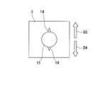
- the external connection terminal is formed with at least one protrusion 14 as shown in FIGS. 2B and 2C.
- FIG. 2C shows a cross section between A2 and A2 in FIG. 2B, but the protrusion 14 is formed lower than the second surface.
- FIG. 2B shows a state in which the protruding portion 14 is formed at one place, and FIG.
- the liquid premold resin 5 is applied to the upper surface of the metal plate in the direction of arrow D5 (FIG. 1D).
- a printing technique for coating from the viewpoint of productivity and quality.
- any method can be used as long as it can be applied appropriately thickly, but screen printing is generally preferable.
- the direction of printing is performed in the directions of the arrow D2 in FIG. 2B and the arrows D3 and D4 in FIG. 2D, so that the flow of the pre-mold resin is given direction and bubbles can be prevented from being involved.
- the premold resin is cured by heating (FIG. 1E).
- the removal method can be selected from dry etching, mechanical polishing, chemical polishing, and the like. Further, the opposite surface was etched to form the semiconductor mounting portion 8, the semiconductor element electrode connection terminal 9, and the wiring 10 to obtain the lead frame substrate 7 (FIG. 1F). A top view of the external connection terminal side is shown in FIG.
- the external connection terminals can be arranged in an array, and it is possible to cope with the increase in the number of pins of the semiconductor element.
- FIG. 4A shows a cross-sectional view in which the semiconductor element 15 is mounted and wire-bonded.
- the semiconductor element 15 is pasted by the die attach material 17 and connected to the semiconductor element electrode connection terminal 9 by the gold wire 16.
- the semiconductor element electrode connection terminal is appropriately subjected to any of nickel-gold plating, tin plating, silver plating, nickel-palladium-gold plating, and the like.
- the lead frame substrate is placed on a heat block and bonded while being heated.
- the premold resin exists on the lower surface of the semiconductor element electrode connection terminal 9 and is hollow. Because the structure is difficult to assemble, it can be assembled without causing poor bonding.
- the semiconductor element side is sealed by transfer molding or potting, and the outer frame portion is separated with a diamond blade or the like to make small pieces (FIG. 4B).
- a semiconductor package using a lead frame substrate can be obtained by mounting solder balls on external connection terminals.
- a BGA (Ball Grid Array) type lead frame substrate will be described with reference to FIGS. 1A to 1F.
- the manufactured BGA has a 10 mm square package size and has a 168-pin array of external connection terminals on the lower surface of the package.
- a long strip-shaped copper alloy metal plate 1 (Furukawa Electric, EFTEC64T) having a width of 150 mm and a thickness of 200 ⁇ m was prepared.
- EFTEC64T Fluukawa Electric
- FIG. 1B on both surfaces of the metal plate 1, a photoresist (manufactured by Tokyo Ohka Kogyo Co., Ltd., OFPR4000) is coated with a roll coater to a thickness of 5 ⁇ m, and then pre-baked at 90 ° C. went.
- pattern exposure is performed from both sides through a photomask having a desired pattern, followed by development with a 1% aqueous sodium carbonate solution, followed by washing with water and post-baking to obtain a photoresist pattern 2 as shown in FIG. 1B. It was.
- a pattern for forming the semiconductor element mounting portion 8, the semiconductor element electrode connection terminal 9, the wiring 10, and the outer frame portion 12 is formed on the first surface, and the protrusion 13 is formed on the second surface.
- a pattern for forming the external connection terminal 11 and the outer frame portion 12 having (FIG. 2A) was formed.
- the shape of the protrusion 13 is an isosceles triangle having a width of 30 ⁇ m in contact with the external connection terminal and a length of 80 ⁇ m.
- a first etching process is performed from the second surface of the metal plate using a ferric chloride solution.
- the thickness of the metal plate portion exposed from the resist pattern on the second surface side was reduced to 30 ⁇ m (FIG. 1C).
- the protrusion part 14 about 40 micrometers in length was able to be formed in the external connection terminal side surface.
- the specific gravity of the ferric chloride solution used was 1.38, and the liquid temperature was 50 ° C.
- thermosetting resin SMC-376KF1, manufactured by Shin-Etsu Chemical Co., Ltd.
- the direction of printing was performed from the place where there was no protrusion 14 to the direction of the protrusion (FIG. 1D). Further, curing was performed at 180 ° C. for 3 hours to form a premold layer 13. The embedding property of the thermosetting resin was good, and no defects including bubbles were observed.
- thermosetting resin layer of about 1 ⁇ m remained on the surfaces of the external connection terminals 11 and the outer frame portion 12 that were not etched, an alkaline aqueous solution of potassium permanganate at 60 ° C. (40 g / L potassium permanganate + 20 g / L sodium hydroxide) was removed by treatment for about 3 minutes.
- a second etching process is performed from the first surface side of the metal plate with a ferric chloride solution to dissolve and remove the metal plate portion exposed from the resist pattern.
- the semiconductor element mounting portion 8, the semiconductor element electrode connection terminal 9, the wiring 10, and the outer frame portion 12 were formed (FIG. 1E).
- the external connection terminal 11 extends from the semiconductor element electrode connection terminal 9.
- the photoresist pattern 2 on the first surface was peeled off to obtain a desired lead frame type BGA substrate 7 (FIG. 1F).
- electrolytic nickel-gold plating was applied to the exposed metal surface.
- the thickness of nickel was 5 ⁇ m, and the thickness of gold was 0.1 ⁇ m (not shown).
- the semiconductor element 15 was mounted on the lead frame type BGA substrate 7 of the present invention using the die attach material 17, and the die attach material was cured at 150 ° C. for 1 hour. Furthermore, the wire of the semiconductor element electrode and the semiconductor element electrode connection terminal 9 were connected by wire bonding using a gold wire 16 having a diameter of 30 ⁇ m (FIG. 4A). When the wire bonding heating temperature was 200 ° C. and the pull strength of the wire on the semiconductor element electrode connection terminal side was measured, it was 9 g or more, and a good connection was obtained.
- the area including the semiconductor element and the semiconductor element electrode connection terminal was transfer-molded and cut into small pieces to obtain a semiconductor package using a lead frame type BGA substrate.
- a lead frame substrate of the present invention By using the method for manufacturing a lead frame substrate of the present invention, it becomes possible to obtain a lead frame substrate with reduced defects during manufacturing and semiconductor package assembly and improved reliability against thermal stress. It is applied to a multi-pin package substrate that cannot be handled by a type of semiconductor package.
Landscapes
- Lead Frames For Integrated Circuits (AREA)
- Die Bonding (AREA)
Priority Applications (2)
| Application Number | Priority Date | Filing Date | Title |
|---|---|---|---|
| CN200980138144.0A CN102165585B (zh) | 2008-09-30 | 2009-09-30 | 引线框基板及其制造方法、半导体器件 |
| US13/064,205 US8558363B2 (en) | 2008-09-30 | 2011-03-10 | Lead frame substrate and method of manufacturing the same, and semiconductor device |
Applications Claiming Priority (2)
| Application Number | Priority Date | Filing Date | Title |
|---|---|---|---|
| JP2008254312A JP5549066B2 (ja) | 2008-09-30 | 2008-09-30 | リードフレーム型基板とその製造方法、及び半導体装置 |
| JP2008-254312 | 2008-09-30 |
Related Child Applications (1)
| Application Number | Title | Priority Date | Filing Date |
|---|---|---|---|
| US13/064,205 Continuation US8558363B2 (en) | 2008-09-30 | 2011-03-10 | Lead frame substrate and method of manufacturing the same, and semiconductor device |
Publications (1)
| Publication Number | Publication Date |
|---|---|
| WO2010038452A1 true WO2010038452A1 (ja) | 2010-04-08 |
Family
ID=42073232
Family Applications (1)
| Application Number | Title | Priority Date | Filing Date |
|---|---|---|---|
| PCT/JP2009/005041 Ceased WO2010038452A1 (ja) | 2008-09-30 | 2009-09-30 | リードフレーム基板とその製造方法、及び半導体装置 |
Country Status (6)
| Country | Link |
|---|---|
| US (1) | US8558363B2 (https=) |
| JP (1) | JP5549066B2 (https=) |
| KR (1) | KR101602982B1 (https=) |
| CN (1) | CN102165585B (https=) |
| TW (1) | TWI502711B (https=) |
| WO (1) | WO2010038452A1 (https=) |
Cited By (2)
| Publication number | Priority date | Publication date | Assignee | Title |
|---|---|---|---|---|
| CN102244060A (zh) * | 2011-06-02 | 2011-11-16 | 日月光半导体制造股份有限公司 | 封装基板及其制造方法 |
| US20120196407A1 (en) * | 2011-01-28 | 2012-08-02 | Shiann-Ming Liou | Single layer bga substrate process |
Families Citing this family (9)
| Publication number | Priority date | Publication date | Assignee | Title |
|---|---|---|---|---|
| TWI427716B (zh) * | 2010-06-04 | 2014-02-21 | 矽品精密工業股份有限公司 | 無載具之半導體封裝件及其製法 |
| US8916421B2 (en) * | 2011-08-31 | 2014-12-23 | Freescale Semiconductor, Inc. | Semiconductor device packaging having pre-encapsulation through via formation using lead frames with attached signal conduits |
| US9142502B2 (en) * | 2011-08-31 | 2015-09-22 | Zhiwei Gong | Semiconductor device packaging having pre-encapsulation through via formation using drop-in signal conduits |
| US8597983B2 (en) | 2011-11-18 | 2013-12-03 | Freescale Semiconductor, Inc. | Semiconductor device packaging having substrate with pre-encapsulation through via formation |
| JP2014072242A (ja) * | 2012-09-27 | 2014-04-21 | Rohm Co Ltd | チップ部品およびその製造方法 |
| KR101505088B1 (ko) * | 2013-10-22 | 2015-03-23 | 앰코 테크놀로지 코리아 주식회사 | 반도체 패키지와 리드프레임 패들 구조 및 방법 |
| JP6266351B2 (ja) * | 2014-01-08 | 2018-01-24 | 新日本無線株式会社 | センサ装置およびその製造方法 |
| JP7182374B2 (ja) * | 2017-05-15 | 2022-12-02 | 新光電気工業株式会社 | リードフレーム及びその製造方法 |
| JP7039245B2 (ja) * | 2017-10-18 | 2022-03-22 | 新光電気工業株式会社 | リードフレーム及びその製造方法と電子部品装置 |
Citations (5)
| Publication number | Priority date | Publication date | Assignee | Title |
|---|---|---|---|---|
| JPH09307043A (ja) * | 1996-05-10 | 1997-11-28 | Dainippon Printing Co Ltd | リードフレーム部材とその製造方法、および該リードフレーム部材を用いた半導体装置 |
| JP2003309242A (ja) * | 2002-04-15 | 2003-10-31 | Dainippon Printing Co Ltd | リードフレーム部材とリードフレーム部材の製造方法、及び該リードフレーム部材を用いた半導体パッケージとその製造方法 |
| JP2003309241A (ja) * | 2002-04-15 | 2003-10-31 | Dainippon Printing Co Ltd | リードフレーム部材とリードフレーム部材の製造方法、及び該リードフレーム部材を用いた半導体パッケージとその製造方法 |
| JP2005117364A (ja) * | 2003-10-08 | 2005-04-28 | Murata Mfg Co Ltd | 弾性表面波装置の製造方法 |
| JP2005175261A (ja) * | 2003-12-12 | 2005-06-30 | Fujitsu Ten Ltd | 基板の電子部品実装構造および方法 |
Family Cites Families (15)
| Publication number | Priority date | Publication date | Assignee | Title |
|---|---|---|---|---|
| JP3642911B2 (ja) | 1997-02-05 | 2005-04-27 | 大日本印刷株式会社 | リードフレーム部材とその製造方法 |
| US6281568B1 (en) * | 1998-10-21 | 2001-08-28 | Amkor Technology, Inc. | Plastic integrated circuit device package and leadframe having partially undercut leads and die pad |
| JP3169919B2 (ja) * | 1998-12-21 | 2001-05-28 | 九州日本電気株式会社 | ボールグリッドアレイ型半導体装置及びその製造方法 |
| MY133357A (en) * | 1999-06-30 | 2007-11-30 | Hitachi Ltd | A semiconductor device and a method of manufacturing the same |
| KR100677651B1 (ko) * | 2001-04-13 | 2007-02-01 | 야마하 가부시키가이샤 | 반도체 소자 및 패키지와 그 제조방법 |
| WO2003007373A1 (en) * | 2001-07-09 | 2003-01-23 | Sumitomo Metal Mining Co., Ltd. | Lead frame and its manufacturing method |
| KR100993277B1 (ko) * | 2002-04-30 | 2010-11-10 | 르네사스 일렉트로닉스 가부시키가이샤 | 반도체장치 및 전자 장치 |
| KR100993579B1 (ko) * | 2002-04-30 | 2010-11-10 | 르네사스 일렉트로닉스 가부시키가이샤 | 반도체장치 및 전자 장치 |
| US7196409B2 (en) * | 2003-03-07 | 2007-03-27 | Nxp B.V. | Semiconductor device, semiconductor body and method of manufacturing thereof |
| JP2004349316A (ja) * | 2003-05-20 | 2004-12-09 | Renesas Technology Corp | 半導体装置及びその製造方法 |
| JP2005191240A (ja) * | 2003-12-25 | 2005-07-14 | Renesas Technology Corp | 半導体装置及びその製造方法 |
| JP4417150B2 (ja) * | 2004-03-23 | 2010-02-17 | 株式会社ルネサステクノロジ | 半導体装置 |
| TWI262587B (en) * | 2005-03-08 | 2006-09-21 | Yi-Ling Jang | Leadframe and the manufacturing method thereof |
| US7687893B2 (en) * | 2006-12-27 | 2010-03-30 | Amkor Technology, Inc. | Semiconductor package having leadframe with exposed anchor pads |
| US8008784B2 (en) * | 2008-10-02 | 2011-08-30 | Advanced Semiconductor Engineering, Inc. | Package including a lead frame, a chip and a sealant |
-
2008
- 2008-09-30 JP JP2008254312A patent/JP5549066B2/ja not_active Expired - Fee Related
-
2009
- 2009-09-29 TW TW098132930A patent/TWI502711B/zh not_active IP Right Cessation
- 2009-09-30 KR KR1020117006885A patent/KR101602982B1/ko not_active Expired - Fee Related
- 2009-09-30 CN CN200980138144.0A patent/CN102165585B/zh not_active Expired - Fee Related
- 2009-09-30 WO PCT/JP2009/005041 patent/WO2010038452A1/ja not_active Ceased
-
2011
- 2011-03-10 US US13/064,205 patent/US8558363B2/en not_active Expired - Fee Related
Patent Citations (5)
| Publication number | Priority date | Publication date | Assignee | Title |
|---|---|---|---|---|
| JPH09307043A (ja) * | 1996-05-10 | 1997-11-28 | Dainippon Printing Co Ltd | リードフレーム部材とその製造方法、および該リードフレーム部材を用いた半導体装置 |
| JP2003309242A (ja) * | 2002-04-15 | 2003-10-31 | Dainippon Printing Co Ltd | リードフレーム部材とリードフレーム部材の製造方法、及び該リードフレーム部材を用いた半導体パッケージとその製造方法 |
| JP2003309241A (ja) * | 2002-04-15 | 2003-10-31 | Dainippon Printing Co Ltd | リードフレーム部材とリードフレーム部材の製造方法、及び該リードフレーム部材を用いた半導体パッケージとその製造方法 |
| JP2005117364A (ja) * | 2003-10-08 | 2005-04-28 | Murata Mfg Co Ltd | 弾性表面波装置の製造方法 |
| JP2005175261A (ja) * | 2003-12-12 | 2005-06-30 | Fujitsu Ten Ltd | 基板の電子部品実装構造および方法 |
Cited By (9)
| Publication number | Priority date | Publication date | Assignee | Title |
|---|---|---|---|---|
| US20120196407A1 (en) * | 2011-01-28 | 2012-08-02 | Shiann-Ming Liou | Single layer bga substrate process |
| WO2012103369A1 (en) * | 2011-01-28 | 2012-08-02 | Marvell World Trade Ltd. | Single layer bga substrate process |
| CN103339716A (zh) * | 2011-01-28 | 2013-10-02 | 马维尔国际贸易有限公司 | 单层bga基板工艺 |
| JP2014504032A (ja) * | 2011-01-28 | 2014-02-13 | マーベル ワールド トレード リミテッド | 単一層bga基板プロセス |
| US8673689B2 (en) | 2011-01-28 | 2014-03-18 | Marvell World Trade Ltd. | Single layer BGA substrate process |
| US8940585B2 (en) | 2011-01-28 | 2015-01-27 | Marvell World Trade Ltd. | Single layer BGA substrate process |
| CN103339716B (zh) * | 2011-01-28 | 2017-04-26 | 马维尔国际贸易有限公司 | 单层bga基板工艺 |
| TWI583267B (zh) * | 2011-01-28 | 2017-05-11 | 馬維爾國際貿易有限公司 | 單層球形柵格陣列基材製程方法 |
| CN102244060A (zh) * | 2011-06-02 | 2011-11-16 | 日月光半导体制造股份有限公司 | 封装基板及其制造方法 |
Also Published As
| Publication number | Publication date |
|---|---|
| JP2010087221A (ja) | 2010-04-15 |
| TW201021186A (en) | 2010-06-01 |
| KR20110074514A (ko) | 2011-06-30 |
| KR101602982B1 (ko) | 2016-03-11 |
| US20110163435A1 (en) | 2011-07-07 |
| JP5549066B2 (ja) | 2014-07-16 |
| US8558363B2 (en) | 2013-10-15 |
| CN102165585B (zh) | 2014-03-26 |
| CN102165585A (zh) | 2011-08-24 |
| TWI502711B (zh) | 2015-10-01 |
Similar Documents
| Publication | Publication Date | Title |
|---|---|---|
| JP5549066B2 (ja) | リードフレーム型基板とその製造方法、及び半導体装置 | |
| JP5532570B2 (ja) | リードフレーム型基板とその製造方法ならびに半導体装置 | |
| JP5407474B2 (ja) | 半導体素子基板の製造方法 | |
| JP5493323B2 (ja) | リードフレーム型基板の製造方法 | |
| CN114695303A (zh) | 引线框架、引线框架的制造方法以及半导体装置 | |
| JP5521301B2 (ja) | リードフレーム型基板とその製造方法および半導体装置 | |
| KR101148100B1 (ko) | 다열형 리드프레임 및 반도체 패키지의 제조방법 | |
| JPH10200009A (ja) | リードフレーム部材とリードフレーム部材の製造方法 |
Legal Events
| Date | Code | Title | Description |
|---|---|---|---|
| WWE | Wipo information: entry into national phase |
Ref document number: 200980138144.0 Country of ref document: CN |
|
| 121 | Ep: the epo has been informed by wipo that ep was designated in this application |
Ref document number: 09817493 Country of ref document: EP Kind code of ref document: A1 |
|
| ENP | Entry into the national phase |
Ref document number: 20117006885 Country of ref document: KR Kind code of ref document: A |
|
| NENP | Non-entry into the national phase |
Ref country code: DE |
|
| 122 | Ep: pct application non-entry in european phase |
Ref document number: 09817493 Country of ref document: EP Kind code of ref document: A1 |