WO2009148009A1 - チップ状電気部品及びその製造方法 - Google Patents
チップ状電気部品及びその製造方法 Download PDFInfo
- Publication number
- WO2009148009A1 WO2009148009A1 PCT/JP2009/059952 JP2009059952W WO2009148009A1 WO 2009148009 A1 WO2009148009 A1 WO 2009148009A1 JP 2009059952 W JP2009059952 W JP 2009059952W WO 2009148009 A1 WO2009148009 A1 WO 2009148009A1
- Authority
- WO
- WIPO (PCT)
- Prior art keywords
- layer
- pair
- conductive layer
- substrate
- plating
- Prior art date
- Legal status (The legal status is an assumption and is not a legal conclusion. Google has not performed a legal analysis and makes no representation as to the accuracy of the status listed.)
- Ceased
Links
Images


Classifications
-
- H—ELECTRICITY
- H01—ELECTRIC ELEMENTS
- H01C—RESISTORS
- H01C7/00—Non-adjustable resistors formed as one or more layers or coatings; Non-adjustable resistors made from powdered conducting material or powdered semi-conducting material with or without insulating material
- H01C7/003—Thick film resistors
-
- H—ELECTRICITY
- H01—ELECTRIC ELEMENTS
- H01C—RESISTORS
- H01C1/00—Details
- H01C1/06—Electrostatic or electromagnetic shielding arrangements
-
- H—ELECTRICITY
- H01—ELECTRIC ELEMENTS
- H01C—RESISTORS
- H01C17/00—Apparatus or processes specially adapted for manufacturing resistors
- H01C17/006—Apparatus or processes specially adapted for manufacturing resistors adapted for manufacturing resistor chips
-
- H—ELECTRICITY
- H01—ELECTRIC ELEMENTS
- H01C—RESISTORS
- H01C17/00—Apparatus or processes specially adapted for manufacturing resistors
- H01C17/06—Apparatus or processes specially adapted for manufacturing resistors adapted for coating resistive material on a base
- H01C17/065—Apparatus or processes specially adapted for manufacturing resistors adapted for coating resistive material on a base by thick film techniques, e.g. serigraphy
- H01C17/06506—Precursor compositions therefor, e.g. pastes, inks, glass frits
-
- Y—GENERAL TAGGING OF NEW TECHNOLOGICAL DEVELOPMENTS; GENERAL TAGGING OF CROSS-SECTIONAL TECHNOLOGIES SPANNING OVER SEVERAL SECTIONS OF THE IPC; TECHNICAL SUBJECTS COVERED BY FORMER USPC CROSS-REFERENCE ART COLLECTIONS [XRACs] AND DIGESTS
- Y10—TECHNICAL SUBJECTS COVERED BY FORMER USPC
- Y10T—TECHNICAL SUBJECTS COVERED BY FORMER US CLASSIFICATION
- Y10T29/00—Metal working
- Y10T29/49—Method of mechanical manufacture
- Y10T29/49002—Electrical device making
- Y10T29/49117—Conductor or circuit manufacturing
- Y10T29/49124—On flat or curved insulated base, e.g., printed circuit, etc.
- Y10T29/49155—Manufacturing circuit on or in base
Definitions
- the present invention relates to a chip-shaped electrical component and a manufacturing method thereof.
- a chip resistor which is a type of chip-shaped electrical component having a relatively large size, has a resistor and the like formed of a thick film, and all of the soldering electrodes are also formed of a thick film.
- Some resistors with relatively small dimensions have electrodes and resistors formed using only a thin film forming technique. Further, some resistors having relatively small dimensions include a soldering electrode formed by a combination of a thick film and a thin film.
- a multi-piece alumina substrate that can be cut and separated is used to obtain individual chip substrates.
- a plurality of thick film resistor layers made of RuO2 are formed by screen printing or the like on the surface of the alumina substrate with a certain interval in the longitudinal direction.
- a plurality of C-shaped side electrodes are formed so as to continuously cover both end portions of the plurality of thick film resistor layers, both side surfaces of the alumina substrate, and both end portions of the back surface of the alumina substrate.
- a thin film forming technique such as sputtering or ion plating is used.
- a glass coat is formed so as to individually cover the entire surface of each resistor.
- This glass coat is formed as a protective film when the resistance value is trimmed.
- laser trimming is performed.
- a protective coat made of glass or the like is individually formed on the surface of each glass coat.
- the alumina substrate is cut into individual chip substrates to complete the manufacture of the chip resistor. According to this conventional method, since the thickness of the electrode can be reduced, the chip resistor can be miniaturized.
- Patent Document 2 a pair of surface electrodes is formed as a thick film on the surface of a ceramic substrate, and a base is formed on the pair of surface electrodes using a thin film forming technique such as sputtering. A structure of a chip resistor in which an electrode layer is formed and a plating layer is further formed on the base electrode layer and a manufacturing method thereof are shown. JP-A 63-172401 JP-A-11-307304
- An object of the present invention is to provide a chip-shaped electrical component that solves the above-described problems.
- a specific object of the present invention is to provide a chip-like electrical component such as a chip resistor that is easy to manufacture and prevents cracks and cracks from entering an insulating substrate without increasing the price.
- a ceramic insulating substrate is used for the chip-like electrical component targeted by the present invention.
- a pair of metal glaze-based surface electrodes are provided at both ends of the substrate surface of the insulating substrate.
- the pair of metal glaze-based surface electrodes can be formed, for example, by printing a paste formed by kneading a conductive powder such as Ag on glass by screen printing.
- the chip-shaped electrical component has an electrical element layer that is electrically connected to the pair of surface electrodes and formed on the substrate surface.
- the electrical element layer is a resistive layer if the chip-like electrical component is a chip resistor. In the case of an inductor, the electric element layer is a conductor layer.
- the chip-like electrical component may be a capacitor or the like.
- the chip-shaped electrical component has an insulating protective layer made of an electrically insulating material that covers the entire electrical element layer and a part of the pair of surface electrodes adjacent to the electrical element layer. Furthermore, the chip-shaped electrical component includes a thin film conductive layer that covers at least a pair of surface electrodes that are not covered by the insulating protective layer. The thin film conductive layer includes one or more plating layers. The surface electrode and the thin film conductive layer constitute a soldering electrode portion.
- the pair of surface electrodes are formed such that the thickness increases from the electric element layer toward the pair of end portions of the insulating substrate positioned in the direction in which the pair of surface electrodes are arranged.
- a plating pool is formed between the surface electrode and the insulating protective layer. Therefore, when one or more plating layers are formed, plating metal accumulates in the plating pool, and the step formed between the soldering electrode portion and the protective layer by the plating layer can be reduced to some extent. Therefore, the step can be reduced without providing an additional layer for reducing the step. As the number of plating layers increases, the step becomes smaller.
- the thin film conductive layer is composed of a base conductive layer that covers the surface electrode that is formed by sputtering or vapor deposition and is not covered by the insulating protective layer, and one or more plated layers formed on the base conductive layer. Is preferred. In this way, the plating layer can be reliably formed only on the base conductive layer.
- the base conductive layer may include a base conductive layer extension that covers the side surface of the end portion of the insulating substrate adjacent to the surface electrode.
- the one or more plating layers include a plating layer extension that covers the base conductive layer extension. Since the plating layer extension constitutes the side electrode of the insulating substrate, the soldering strength is increased.
- the base conductive layer extension part may further partially extend on the back surface of the insulating substrate facing the substrate surface. Also in this case, a part of the plating layer extension extends on the base conductive layer extension extending on the back surface of the substrate. As a result, the plating layer extension formed on the back side of the substrate serves as the back electrode of the insulating substrate, so that the soldering strength can be further increased.
- the base conductive layer preferably contains Cu, Ni, and Cr.
- the one or more plating layers preferably have a two-layer structure in which a Sn plating layer is formed on a Ni plating layer. With such a structure, the base conductive layer and the plating layer can be reliably formed.
- the electrical element layer may be configured with a resistance layer. And it is preferable to comprise an insulating protective layer from the glass layer which covers a resistance layer, and the insulating resin layer which covers a glass layer. In this way, it is possible to prevent the resistance value of the resistance layer from changing after the resistance layer is trimmed.
- the method for manufacturing a chip-shaped electrical component of the present invention includes the following steps.
- a plurality of electrode layers are arranged in a vertical electrode layer row and a horizontal electrode layer by screen printing using a metal glaze-type conductive paste at predetermined intervals on the substrate surface of a large ceramic insulating substrate.
- Form to form a column In the next step, the electric element layer is formed on the substrate surface of the large insulating substrate by printing so as to straddle a pair of adjacent electrode layers of the plurality of electrode layers included in the horizontal electrode layer row.
- an insulating protective layer is formed by printing using an electric insulating material so as to cover the entire electric element layer and a part of the pair of electrode layers adjacent to the electric element layer.
- a plurality of electrode layers included in the vertical electrode layer sequence are divided into two at the central portion, and a plurality of slits are formed in the large insulating substrate to form a pair of surface electrodes at both ends of the electric element layer.
- a base conductive layer that covers the inner surfaces of the pair of surface electrodes and slits not covered with the insulating protective layer is formed by sputtering or vapor deposition.
- the chip piece including the pair of surface electrodes, the electric element layer, and the insulating protective layer is separated.
- one or more plating layers are formed on the underlying conductive layer of the separated chip pieces.
- the electrode layer formed by screen printing has a dome shape in which the height of the central portion is the highest or a shape that is smoothly convex upward.
- a shape in which the thickness increases as the pair of surface electrodes moves toward the pair of end portions of the insulating substrate can be easily formed.
- FIGS. 2A and 2B are an enlarged sectional view taken along line IIIA-IIIA in FIG. 2D and an enlarged sectional view taken along line IIIB-IIIB in FIG. It is sectional drawing which shows schematically the structure of other embodiment of this invention.
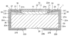
- FIG. 1 is a cross-sectional view schematically showing the structure of a chip resistor 1 which is a kind of chip-shaped electrical component manufactured by the chip-shaped electrical component manufacturing method of the present invention.
- FIG. 1 is a schematic cross-sectional view for ease of understanding, and the dimensional ratio of each part and the thickness and shape of each layer are different from those of an actual part.
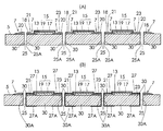
- 2A to 2F are process diagrams showing a plurality of processes in the method of manufacturing the chip resistor 1 according to the embodiment of FIG. The structure of the chip resistor 1 shown in FIG. 1 will be described together with the manufacturing method of the chip resistor 1 of the present embodiment using the process diagram of FIG.
- reference numeral 3 denotes a large-sized insulating substrate made of a ceramic substrate.
- a conductive glass paste (metal glaze type) is formed on the substrate surface 5 of the large insulating substrate 3 with predetermined intervals in the X direction (horizontal direction) and Y direction (vertical direction) shown in FIG.
- a plurality of electrode layers 7 are formed to form the vertical electrode layer rows 9 and the horizontal electrode layer rows 11 by screen printing using the conductive paste.
- 4 ⁇ 4 electrode layers 7 are shown, but more electrode layers 7 are actually formed.
- the conductive glass paste for example, an Ag—Pd glass paste containing silver is used. In this example, this conductive glass paste is baked at a temperature of about 850 ° C.
- the plurality of electrode layers 7 have a length in the horizontal direction that is longer than a length in the vertical direction. This is because the electrode layer 7 is later divided into two.
- the electrode layer 7 formed by screen printing has a shape in which the height dimension of the central portion of the printed portion of the conductive glass paste printed by surface tension is the highest, and smoothly protrudes upward. It is baked in the shape that became a shape, or a shape resembling a mountain that gradually increases in height from the base toward the top.
- a pair of surface electrodes 21 and 23 provided on both ends 18 and 20 of the substrate surface 29A of the insulating substrate 29 are obtained as shown in FIG.
- the resistance as an electric element layer so as to straddle a pair of adjacent electrode layers 7, 7 of the plurality of electrode layers 7 included in the horizontal electrode layer sequence 11.
- the layer 13 is formed on the substrate surface 5 of the large insulating substrate 3 by printing.
- the resistance layer 13 is formed from a resistor glass paste whose main component is a metal oxide such as ruthenium oxide using glass as a binder.
- a resistor pattern is printed on the substrate surface 5 of the large insulating substrate 3 by screen printing using this resistor glass paste, and this is fired at a firing temperature of about 850 ° C. to form a thick resistive layer 13. Forming.
- the resistance layer 13 is printed by printing so as to cover the entire resistance layer 13 and a part of the pair of electrode layers 7 and 7 adjacent to the resistance layer 13.
- An insulating protective layer 15 including a glass layer 17 to be covered and an insulating resin layer 19 to cover the glass layer 17 is formed.
- the insulating protection layer 15 covers the entire resistance layer 13 (electric element layer) and a part of the pair of surface electrodes 21 and 23 adjacent to the resistance layer 13, that is, the portions 21 ⁇ / b> A and 23 ⁇ / b> A. ing.
- the resistance layer 13 is covered with the glass layer 17, the resistance layer 13 is formed with a trimming groove by a laser beam to adjust the resistance value (trimming), and then the insulating resin layer 19 is formed. It is possible to prevent the resistance value 13 from fluctuating.
- Both the glass layer 17 and the insulating resin layer 19 are formed by screen printing.
- the glass layer 17 is fired at a firing temperature of about 850 ° C.
- the insulating resin layer 19 is formed using a synthetic resin paste such as an epoxy resin or a phenol resin, and the firing temperature is about 200 ° C.
- FIGS. 2D and 3A an enlarged cross-sectional view taken along line IIIA-IIIA in FIG. 2D
- a plurality of layers included in the vertical electrode layer row 9 are included.
- a plurality of slits 25 are formed in the large insulating substrate 3.
- FIGS. 2E and 3B an enlarged cross-sectional view taken along line IIIB-IIIB in FIG. 2E]
- a pair of surface electrodes 21 and 23 not covered with the insulating protective layer 15 are used.
- the base conductive layer 27 which covers the inner surface 25A of the slit 25 and a part of the back surface of the large-sized insulating substrate 3 is formed by sputtering or vapor deposition.
- the underlying conductive layer 27 is an alloy layer containing Cu, Ni, and Cr. These metals have the property that plating metal is easy to adhere.
- the base conductive layer 27 covers the side conductive layer 27 on the side surface 30A of the end 30 of the insulating substrate 29 adjacent to the surface electrodes 21 and 23. 27A.
- the base conductive layer extension 27 ⁇ / b> A partially extends 27 ⁇ / b> B on the substrate back surface 29 ⁇ / b> B facing the substrate surface 29 ⁇ / b> A of the insulating substrate 29.
- an appropriate mask may be formed on the front surface and the back surface of the large insulating substrate 3.
- the chip piece 31 including the pair of surface electrodes 21 and 23, the resistance layer 13, and the insulating protective layer 15 is separated from the large insulating substrate 3 on the substrate surface 5 of the insulating substrate 29 made of a ceramic substrate. Is done.
- plating layers 33 are formed on the underlying conductive layer 27 of the separated chip pieces 31.
- the plated layer 33 is also formed on the underlying conductive layer extension 27A of the underlying conductive layer 27, and the portion of the plated layer 33 formed on the underlying conductive layer extension 27A constitutes the plated layer extension 33A.
- the plating layer 33 has a two-layer structure in which an Sn plating layer 37 is formed on an Ni plating layer 35 formed by electroless plating.
- the base conductive layer 27 and the plating layer 33 thus formed constitute a thin film conductive layer 32 as shown in FIG.
- the plating layer 33 is also formed on the base conductive layer extension 27A of the base conductive layer 27 as shown in FIG. 1, and the portion of the plating layer 33 formed on the base conductive layer extension 27A is plated.
- the layer extension 33A is configured.
- a part 33B of the plating layer extension 33A extends on a part 27B of the base conductive layer extension 27A extending on the substrate back surface 29B of the insulating substrate 29.
- the pair of surface electrodes 21 and 23 are positioned in the direction in which the pair of surface electrodes 21 and 23 are arranged from the resistance layer 13.
- the thickness increases toward the pair of end portions 30.
- a plating pool S is formed between the surface electrode 21 or 23 and the insulating protective layer 15. Therefore, when one or more plating layers 33 (35 and 37) are formed, plating metal is accumulated in the plating reservoir S, and the soldering electrode portions (21, 23, 27, 33) and the insulating protective layer 15 are accumulated by the plating layer 33. Can be reduced to some extent. Therefore, according to the present embodiment, the step can be reduced without providing an additional layer for reducing the step as in the prior art. As the number of plating layers 33 increases, the step becomes smaller.
- FIG. 4 is a cross-sectional view schematically showing the structure of a chip resistor 101 according to another embodiment of the present invention.
- the same parts as those in the embodiment shown in FIG. 1 are denoted by the same reference numerals as those in FIG.
- the base conductive layer extension 127A extends on the side surface 130 of the insulating substrate 129, but the base conductive layer extension 127A does not extend on the back surface 129B side.
- the present invention can also be applied to such a case. Further, the present invention can naturally be applied even when the conductive extension 127A is not provided.
- the insulating protective layers 15 and 115 have a two-layer structure, but a single-layer structure may be used.
- the pair of surface electrodes are formed so that the thickness increases from the electric element layer toward the pair of end portions of the insulating substrate positioned in the direction in which the pair of surface electrodes are arranged.
- a plating pool is formed between the surface electrode and the insulating protective layer. Therefore, when one or more plating layers are formed, plating metal accumulates in the plating pool, and the step formed between the soldering electrode portion and the protective layer by the plating layer can be reduced to some extent. Therefore, the step can be reduced without providing an additional layer for reducing the step. As the number of plating layers increases, the step becomes smaller.
- the manufacturing method of the present invention since the method of dividing the electrode layer into two at the central portion is adopted, a shape in which the thickness of the pair of surface electrodes increases as it goes toward the pair of end portions of the insulating substrate can be easily formed. Can do.
Landscapes
- Engineering & Computer Science (AREA)
- Microelectronics & Electronic Packaging (AREA)
- Physics & Mathematics (AREA)
- Electromagnetism (AREA)
- Manufacturing & Machinery (AREA)
- Non-Adjustable Resistors (AREA)
- Apparatuses And Processes For Manufacturing Resistors (AREA)
- Details Of Resistors (AREA)
Priority Applications (2)
| Application Number | Priority Date | Filing Date | Title |
|---|---|---|---|
| US12/995,867 US8193899B2 (en) | 2008-06-05 | 2009-06-01 | Chip-like electric component and method for manufacturing the same |
| CN200980120385.2A CN102057448B (zh) | 2008-06-05 | 2009-06-01 | 芯片状电气部件及其制造方法 |
Applications Claiming Priority (2)
| Application Number | Priority Date | Filing Date | Title |
|---|---|---|---|
| JP2008148287A JP4498433B2 (ja) | 2008-06-05 | 2008-06-05 | チップ状電気部品及びその製造方法 |
| JP2008-148287 | 2008-06-05 |
Publications (1)
| Publication Number | Publication Date |
|---|---|
| WO2009148009A1 true WO2009148009A1 (ja) | 2009-12-10 |
Family
ID=41398087
Family Applications (1)
| Application Number | Title | Priority Date | Filing Date |
|---|---|---|---|
| PCT/JP2009/059952 Ceased WO2009148009A1 (ja) | 2008-06-05 | 2009-06-01 | チップ状電気部品及びその製造方法 |
Country Status (4)
| Country | Link |
|---|---|
| US (1) | US8193899B2 (enExample) |
| JP (1) | JP4498433B2 (enExample) |
| CN (1) | CN102057448B (enExample) |
| WO (1) | WO2009148009A1 (enExample) |
Families Citing this family (15)
| Publication number | Priority date | Publication date | Assignee | Title |
|---|---|---|---|---|
| US8466548B2 (en) | 2011-05-31 | 2013-06-18 | Infineon Technologies Ag | Semiconductor device including excess solder |
| JP6285096B2 (ja) | 2011-12-26 | 2018-02-28 | ローム株式会社 | チップ抵抗器、および、電子デバイス |
| JP2014135427A (ja) * | 2013-01-11 | 2014-07-24 | Koa Corp | チップ抵抗器 |
| CN104347208B (zh) * | 2013-07-31 | 2018-10-12 | 南京中兴新软件有限责任公司 | 一种电阻器制作方法、电阻器及电路 |
| JP6258116B2 (ja) * | 2014-04-25 | 2018-01-10 | Koa株式会社 | 抵抗器の製造方法 |
| JP6373723B2 (ja) * | 2014-10-31 | 2018-08-15 | Koa株式会社 | チップ抵抗器 |
| US9997281B2 (en) | 2015-02-19 | 2018-06-12 | Rohm Co., Ltd. | Chip resistor and method for manufacturing the same |
| WO2016171244A1 (ja) * | 2015-04-24 | 2016-10-27 | 釜屋電機株式会社 | 角形チップ抵抗器及びその製造法 |
| CN114864200A (zh) * | 2016-12-27 | 2022-08-05 | 罗姆股份有限公司 | 片式电阻器 |
| CN111344818B (zh) | 2017-11-02 | 2022-06-03 | 罗姆股份有限公司 | 片式电阻器 |
| JP7602912B2 (ja) * | 2018-07-02 | 2024-12-19 | 北陸電気工業株式会社 | ネットワークチップ抵抗器 |
| CN114449727B (zh) * | 2020-10-30 | 2024-10-22 | 礼鼎半导体科技秦皇岛有限公司 | 线路板及其制备方法 |
| KR102815928B1 (ko) * | 2021-02-25 | 2025-06-02 | 삼성전기주식회사 | 칩 저항 부품 |
| JP2022189034A (ja) * | 2021-06-10 | 2022-12-22 | Koa株式会社 | チップ抵抗器およびチップ抵抗器の製造方法 |
| JP7759197B2 (ja) * | 2021-06-10 | 2025-10-23 | Koa株式会社 | チップ部品 |
Citations (8)
| Publication number | Priority date | Publication date | Assignee | Title |
|---|---|---|---|---|
| JPS63188903A (ja) * | 1987-01-31 | 1988-08-04 | 住友電気工業株式会社 | 薄膜抵抗素子 |
| JP2000091101A (ja) * | 1998-09-16 | 2000-03-31 | Matsushita Electric Ind Co Ltd | 抵抗器およびその製造方法 |
| JP2004158696A (ja) * | 2002-11-07 | 2004-06-03 | Matsushita Electric Ind Co Ltd | 薄膜回路基板及びその製造方法及び薄膜デバイス |
| JP2004259863A (ja) * | 2003-02-25 | 2004-09-16 | Rohm Co Ltd | チップ抵抗器 |
| JP2004288806A (ja) * | 2003-03-20 | 2004-10-14 | Matsushita Electric Ind Co Ltd | 多層プリント配線板の製造方法 |
| JP2007042953A (ja) * | 2005-08-04 | 2007-02-15 | Rohm Co Ltd | チップ型電子部品 |
| JP2007189122A (ja) * | 2006-01-16 | 2007-07-26 | Matsushita Electric Ind Co Ltd | チップ形電子部品 |
| JP2008084905A (ja) * | 2006-09-26 | 2008-04-10 | Taiyosha Electric Co Ltd | チップ抵抗器 |
Family Cites Families (8)
| Publication number | Priority date | Publication date | Assignee | Title |
|---|---|---|---|---|
| JPS63172401A (ja) | 1987-01-12 | 1988-07-16 | ティーディーケイ株式会社 | チツプ抵抗器、その集合体及びチツプ抵抗器の製造方法 |
| US4792781A (en) * | 1986-02-21 | 1988-12-20 | Tdk Corporation | Chip-type resistor |
| JP3254866B2 (ja) * | 1993-12-21 | 2002-02-12 | 株式会社村田製作所 | 誘電体共振器およびその製造方法 |
| TW424245B (en) * | 1998-01-08 | 2001-03-01 | Matsushita Electric Industrial Co Ltd | Resistor and its manufacturing method |
| JPH11307304A (ja) | 1998-04-20 | 1999-11-05 | Hokuriku Electric Ind Co Ltd | チップ抵抗器及びその製造方法 |
| WO2004023498A1 (en) * | 2002-09-03 | 2004-03-18 | Vishay Intertechnology, Inc. | Flip chip resistor and its manufacturing method |
| JP2004288808A (ja) * | 2003-03-20 | 2004-10-14 | Matsushita Electric Ind Co Ltd | 抵抗器の製造方法 |
| JP3983264B2 (ja) * | 2005-09-27 | 2007-09-26 | 北陸電気工業株式会社 | チップ状電気部品の端子構造 |
-
2008
- 2008-06-05 JP JP2008148287A patent/JP4498433B2/ja not_active Expired - Fee Related
-
2009
- 2009-06-01 WO PCT/JP2009/059952 patent/WO2009148009A1/ja not_active Ceased
- 2009-06-01 US US12/995,867 patent/US8193899B2/en not_active Expired - Fee Related
- 2009-06-01 CN CN200980120385.2A patent/CN102057448B/zh not_active Expired - Fee Related
Patent Citations (8)
| Publication number | Priority date | Publication date | Assignee | Title |
|---|---|---|---|---|
| JPS63188903A (ja) * | 1987-01-31 | 1988-08-04 | 住友電気工業株式会社 | 薄膜抵抗素子 |
| JP2000091101A (ja) * | 1998-09-16 | 2000-03-31 | Matsushita Electric Ind Co Ltd | 抵抗器およびその製造方法 |
| JP2004158696A (ja) * | 2002-11-07 | 2004-06-03 | Matsushita Electric Ind Co Ltd | 薄膜回路基板及びその製造方法及び薄膜デバイス |
| JP2004259863A (ja) * | 2003-02-25 | 2004-09-16 | Rohm Co Ltd | チップ抵抗器 |
| JP2004288806A (ja) * | 2003-03-20 | 2004-10-14 | Matsushita Electric Ind Co Ltd | 多層プリント配線板の製造方法 |
| JP2007042953A (ja) * | 2005-08-04 | 2007-02-15 | Rohm Co Ltd | チップ型電子部品 |
| JP2007189122A (ja) * | 2006-01-16 | 2007-07-26 | Matsushita Electric Ind Co Ltd | チップ形電子部品 |
| JP2008084905A (ja) * | 2006-09-26 | 2008-04-10 | Taiyosha Electric Co Ltd | チップ抵抗器 |
Also Published As
| Publication number | Publication date |
|---|---|
| US8193899B2 (en) | 2012-06-05 |
| CN102057448A (zh) | 2011-05-11 |
| CN102057448B (zh) | 2014-03-12 |
| US20110080251A1 (en) | 2011-04-07 |
| JP2009295813A (ja) | 2009-12-17 |
| JP4498433B2 (ja) | 2010-07-07 |
Similar Documents
| Publication | Publication Date | Title |
|---|---|---|
| JP4498433B2 (ja) | チップ状電気部品及びその製造方法 | |
| JP2009295813A5 (enExample) | ||
| KR100468373B1 (ko) | 저항기 및 그 제조 방법 | |
| US20180158578A1 (en) | Chip Resistor | |
| JP5115968B2 (ja) | チップ抵抗器の製造方法およびチップ抵抗器 | |
| JP3846312B2 (ja) | 多連チップ抵抗器の製造方法 | |
| US9832877B2 (en) | Collective substrate for resistor devices | |
| JP5249566B2 (ja) | チップ抵抗器及びチップ抵抗器の製造方法 | |
| KR20080031982A (ko) | 칩 저항기 및 그 제조 방법 | |
| JP4729398B2 (ja) | チップ抵抗器 | |
| JP2005191406A (ja) | チップ抵抗器およびその製造方法 | |
| JP7790924B2 (ja) | チップ抵抗器の製造方法 | |
| JP2017228701A (ja) | チップ抵抗器およびチップ抵抗器の実装構造 | |
| JP2005108865A (ja) | チップ抵抗器及びチップ抵抗器の製造方法 | |
| CN106205913B (zh) | 覆盖引线型电子部件及其制造方法 | |
| US20180096759A1 (en) | Chip resistor and method for manufacturing the same | |
| JP3608570B2 (ja) | 抵抗器の製造方法 | |
| JP4059967B2 (ja) | チップ型複合機能部品 | |
| JP6551346B2 (ja) | 電子部品及び電子部品の製造方法 | |
| JP7197393B2 (ja) | 硫化検出センサおよびその製造方法 | |
| JPH11307304A (ja) | チップ抵抗器及びその製造方法 | |
| JP6688035B2 (ja) | チップ抵抗器 | |
| JP4526117B2 (ja) | 低い抵抗値を有するチップ抵抗器とその製造方法 | |
| JP2005191402A (ja) | チップ抵抗器、チップ部品及びチップ抵抗器の製造方法 | |
| WO2006022055A1 (ja) | チップ型部品とその製造方法 |
Legal Events
| Date | Code | Title | Description |
|---|---|---|---|
| WWE | Wipo information: entry into national phase |
Ref document number: 200980120385.2 Country of ref document: CN |
|
| 121 | Ep: the epo has been informed by wipo that ep was designated in this application |
Ref document number: 09758276 Country of ref document: EP Kind code of ref document: A1 |
|
| WWE | Wipo information: entry into national phase |
Ref document number: 12995867 Country of ref document: US |
|
| NENP | Non-entry into the national phase |
Ref country code: DE |
|
| 122 | Ep: pct application non-entry in european phase |
Ref document number: 09758276 Country of ref document: EP Kind code of ref document: A1 |