US9577018B2 - Display unit and electronic apparatus - Google Patents
Display unit and electronic apparatus Download PDFInfo
- Publication number
- US9577018B2 US9577018B2 US14/541,774 US201414541774A US9577018B2 US 9577018 B2 US9577018 B2 US 9577018B2 US 201414541774 A US201414541774 A US 201414541774A US 9577018 B2 US9577018 B2 US 9577018B2
- Authority
- US
- United States
- Prior art keywords
- shielding film
- light shielding
- display unit
- partition
- light
- Prior art date
- Legal status (The legal status is an assumption and is not a legal conclusion. Google has not performed a legal analysis and makes no representation as to the accuracy of the status listed.)
- Active, expires
Links
Images


Classifications
-
- H—ELECTRICITY
- H10—SEMICONDUCTOR DEVICES; ELECTRIC SOLID-STATE DEVICES NOT OTHERWISE PROVIDED FOR
- H10K—ORGANIC ELECTRIC SOLID-STATE DEVICES
- H10K59/00—Integrated devices, or assemblies of multiple devices, comprising at least one organic light-emitting element covered by group H10K50/00
- H10K59/10—OLED displays
- H10K59/12—Active-matrix OLED [AMOLED] displays
- H10K59/126—Shielding, e.g. light-blocking means over the TFTs
-
- H—ELECTRICITY
- H10—SEMICONDUCTOR DEVICES; ELECTRIC SOLID-STATE DEVICES NOT OTHERWISE PROVIDED FOR
- H10K—ORGANIC ELECTRIC SOLID-STATE DEVICES
- H10K50/00—Organic light-emitting devices
- H10K50/80—Constructional details
- H10K50/86—Arrangements for improving contrast, e.g. preventing reflection of ambient light
- H10K50/865—Arrangements for improving contrast, e.g. preventing reflection of ambient light comprising light absorbing layers, e.g. light-blocking layers
-
- H01L27/3272—
-
- H01L27/3246—
-
- H—ELECTRICITY
- H10—SEMICONDUCTOR DEVICES; ELECTRIC SOLID-STATE DEVICES NOT OTHERWISE PROVIDED FOR
- H10K—ORGANIC ELECTRIC SOLID-STATE DEVICES
- H10K50/00—Organic light-emitting devices
- H10K50/80—Constructional details
- H10K50/805—Electrodes
- H10K50/82—Cathodes
-
- H—ELECTRICITY
- H10—SEMICONDUCTOR DEVICES; ELECTRIC SOLID-STATE DEVICES NOT OTHERWISE PROVIDED FOR
- H10K—ORGANIC ELECTRIC SOLID-STATE DEVICES
- H10K50/00—Organic light-emitting devices
- H10K50/80—Constructional details
- H10K50/84—Passivation; Containers; Encapsulations
- H10K50/841—Self-supporting sealing arrangements
-
- H—ELECTRICITY
- H10—SEMICONDUCTOR DEVICES; ELECTRIC SOLID-STATE DEVICES NOT OTHERWISE PROVIDED FOR
- H10K—ORGANIC ELECTRIC SOLID-STATE DEVICES
- H10K59/00—Integrated devices, or assemblies of multiple devices, comprising at least one organic light-emitting element covered by group H10K50/00
- H10K59/10—OLED displays
- H10K59/12—Active-matrix OLED [AMOLED] displays
- H10K59/122—Pixel-defining structures or layers, e.g. banks
-
- H—ELECTRICITY
- H10—SEMICONDUCTOR DEVICES; ELECTRIC SOLID-STATE DEVICES NOT OTHERWISE PROVIDED FOR
- H10K—ORGANIC ELECTRIC SOLID-STATE DEVICES
- H10K59/00—Integrated devices, or assemblies of multiple devices, comprising at least one organic light-emitting element covered by group H10K50/00
- H10K59/30—Devices specially adapted for multicolour light emission
- H10K59/35—Devices specially adapted for multicolour light emission comprising red-green-blue [RGB] subpixels
-
- H—ELECTRICITY
- H10—SEMICONDUCTOR DEVICES; ELECTRIC SOLID-STATE DEVICES NOT OTHERWISE PROVIDED FOR
- H10K—ORGANIC ELECTRIC SOLID-STATE DEVICES
- H10K59/00—Integrated devices, or assemblies of multiple devices, comprising at least one organic light-emitting element covered by group H10K50/00
- H10K59/30—Devices specially adapted for multicolour light emission
- H10K59/38—Devices specially adapted for multicolour light emission comprising colour filters or colour changing media [CCM]
-
- H01L51/5284—
-
- H—ELECTRICITY
- H10—SEMICONDUCTOR DEVICES; ELECTRIC SOLID-STATE DEVICES NOT OTHERWISE PROVIDED FOR
- H10K—ORGANIC ELECTRIC SOLID-STATE DEVICES
- H10K2102/00—Constructional details relating to the organic devices covered by this subclass
Definitions
- the present disclosure relates to a display unit emitting light with use of organic electroluminescence (EL) phenomenon, and to an electronic apparatus provided with the display unit.
- EL organic electroluminescence
- an organic EL element attracting attention as a next generation display element has advantages of high response speed in addition to wide viewing angle and excellent contrast, as a self-light-emitting display element.
- a display unit provided with the organic EL elements (the light emitting elements)
- the organic EL element emitting red light (a red pixel R), green light (a green pixel G), or blue light (a blue pixel B) is provided in each of the pixels.
- a color element a color filter corresponding to each color pixel is provided on a counter surface of each organic EL element, which improves color purity of light extracted from the display unit.
- a black matrix is provided between color elements in order to prevent color mixture from adjacent color pixels.
- light emitted from a light emitting element in an oblique direction passes through the black matrix and enters the color pixels adjacently provided (adjacent color pixels), and thus causes degradation of color purity. Therefore, for example, in Japanese Unexamined Patent Application Publication Nos. 2005-294057 and 2005-293946, display units in which a black matrix is formed to have a thickness larger than that of a color filter to shield obliquely-entering light are disclosed. Moreover, for example, in Japanese Unexamined Patent Application Publication Nos.
- a display unit including: a drive substrate having a plurality of pixels with a partition therebetween; and a first light shielding film provided on the partition.
- an electronic apparatus provided with a display unit.
- the display unit includes: a drive circuit having a plurality of pixels with a partition therebetween; and a first light shielding film provided on the partition.
- the first shielding film is provided on the partition that is provided between the pixels, which suppresses entering, to the adjacent color pixels (specifically, the color pixels adjacently provided), of emitted light (obliquely-emitted light) that is emitted at a large emission angle and thus may enter the adjacent pixels.
- the first light shielding film is provided on the partition provided between the pixels. Therefore, it is possible to shield the obliquely-emitted light to prevent occurrence of color mixture in the adjacent color pixels. Consequently, it is possible to provide the display unit and the electronic apparatus that have high chromaticity viewing angle and high color reproducibility. Note that the effects described here are not necessarily limited, and effects described in the present disclosure may be obtained.
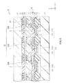
- FIG. 1 is a sectional diagram illustrating a structure of a display unit according to a first embodiment of the disclosure.
- FIG. 2 is a plan view illustrating a shape of a light shielding film in the display unit illustrated in FIG. 1 .
- FIG. 3 is a schematic diagram explaining an effect of the display unit illustrated in FIG. 1 .
- FIG. 4 is a diagram illustrating an entire configuration of the display unit illustrated in FIG. 1 .
- FIG. 5 is a circuit diagram illustrating an example of a pixel drive circuit illustrated in FIG. 4 .
- FIG. 6 is a sectional diagram illustrating a structure of a display unit according to a second embodiment of the disclosure.
- FIG. 7 is a schematic diagram explaining an effect of the display unit illustrated in FIG. 6 .
- FIG. 8 is a sectional diagram illustrating a structure of a display unit according to a modification of the first embodiment of the disclosure.
- FIG. 9 is a sectional diagram illustrating a structure of a display unit according to a modification of the second embodiment of the disclosure.
- FIG. 10 is a sectional diagram illustrating a structure of a display unit according to a third embodiment of the disclosure.
- FIG. 11A is a perspective view illustrating an example of an appearance of an application example 1 of the display unit according to any of the above-described embodiments and the like.
- FIG. 11B is a perspective view illustrating another example of the appearance of the application example 1 illustrated in FIG. 11A .
- FIG. 12 is a perspective view illustrating an appearance of an application example 2.
- FIG. 13A is a front view, a left side view, a right side view, a top view, and a bottom view of an application example 3 in a closed state.
- FIG. 13B is a front view and a side view of the application example 3 illustrated in FIG. 13A in an open state.
- FIG. 1 illustrates an example of a sectional structure of a display unit (a display unit 1 ) according to a first embodiment of the disclosure.
- the display unit 1 may be used as, for example, a television receiver, and as illustrated in FIG. 4 , a display region 110 A and a peripheral region 110 B that is provided on the periphery thereof are provided on a drive substrate 11 .
- the display unit 1 includes a plurality of pixels 2 (for example, a red pixel 2 R, a green pixel 2 G, and a blue pixel 2 B) that are arranged in a matrix in the display region 110 A.
- a light emitting element 10 (a red light emitting element 10 R, a green light emitting element 10 G, and a blue light emitting element 10 B, respectively) emitting corresponding single light (red light LR, green light LG, and blue light LB, respectively) is provided.
- the display unit 1 is a display unit of a top light emission type (so-called top emission type) that allows light emitted from the light emitting element 10 to be extracted from a top surface (a surface on a side opposite to the drive substrate 11 ) side.
- the peripheral region 110 B is provided with a signal line drive circuit 120 and a scan line drive circuit 130 that are drivers for picture display.
- each of the pixels 2 R, 2 G, and 2 B is segmented by a partition 13 provided on the drive substrate 11 .
- Color filters (CF) 22 R, 22 G, and 22 B are provided on positions corresponding to the respective pixels 2 R, 2 G, and 2 B (on the light emitting elements 10 R, 10 G, and 10 B) on a counter surface of a counter substrate 20 that is provided oppositely to the drive substrate 11 .
- a black matrix (BM) 21 that prevents color mixture from adjacent color pixels is provided between the CFs 22 R, 22 G, and 22 B.
- the display unit 1 has a structure in which a light shielding film 14 (a first light shielding film) is provided on a top surface (specifically, a position facing the BM 21 ) of the partition 13 .
- Each of the light emitting elements 10 R, 10 G, and 10 B has a pixel electrode 12 as an anode, an organic layer 15 including a light emitting layer 15 B, and a counter electrode 16 as a cathode that are stacked in order from the drive substrate 11 side provided with a drive transistor Tr 1 and the like of the pixel drive circuit 140 (see FIG. 4 and FIG. 5 ).
- the partition 13 is provided between the light emitting elements 10 R, 10 G, and 10 B, and the above-described light shielding film 14 is provided on the partition 13 and between the partition 13 and the organic layer 15 configuring the light emitting element 10 .
- Such light emitting elements 10 R, 10 G, and 10 B are covered with a protection film 17 and a planarizing film 18 , and further, the counter substrate 20 is bonded to the entire planarizing film 18 with an adhesive layer (not illustrated) in between.
- the counter substrate 20 has the BM 21 and the CF 22 on the counter surface to the drive substrate 11 , and an overcoat (OC) 23 is provided on the CF 22 .
- the pixel electrode 12 also has a function as a reflection layer, and may desirably have a reflectance as high as possible in order to enhance light emission efficiency.
- the pixel electrode 12 may be desirably formed of a material with higher hole injection property.
- such a pixel electrode 12 may have a thickness in a stacked-layer direction (in the X-axis direction) (hereinafter, simply referred to as a thickness) of about 100 nm or more and about 1000 nm or less, and may be formed of a simple substance of a metal element of chromium (Cr), gold (Au), platinum (Pt), nickel (Ni), copper (Cu), tungsten (W), silver (Ag), and the like or an alloy containing any of these metal elements.
- a transparent conductive film formed of an indium tin oxide (ITO) or the like may be provided on a surface of the pixel electrode 12 .
- a material that has an issue of a hole injection barrier due to presence of an oxide film on the surface thereof and small work function while having high reflectance may be used as the pixel electrode 12 by providing an appropriate hole injection layer.
- the partition 13 segments the pixels 2 R, 2 G, and 2 B as described above, and electrically separates the light emitting elements 10 R, 10 G, and 10 B from one another.
- An opening section 13 A that is a light emitting region for each of the pixels 2 R, 2 G, and 2 B is provided in the partition 13 .
- an organic layer 15 including a light emitting layer 15 B (a red light emitting layer 15 BR, a green light emitting layer 15 BG, or a blue light emitting layer 15 BB) configuring the corresponding light emitting element 10 R, 10 G, or 10 B is provided in the opening section 13 A.
- Examples of the material of the partition 13 may include, for example, an organic material such as polyimide, a novolak resin, and an acrylic resin.
- the material of the partition 13 is not limited thereto, and for example, the organic material and an inorganic material may be combined and used.
- Examples of the inorganic material may include SiO 2 , SiO, SiC, and SiN.
- the partition 13 may be formed as a single layer film of the above-described organic material, may be formed to have a stacked-layer structure of an organic film and an inorganic film when the organic material and the inorganic material are combined.
- the organic layer 15 and the counter electrode 16 are provided also on the partition 13 ; however, light is emitted from only the light emitting region.
- the partition 13 includes the top surface that has a flat plane parallel to the drive substrate 11 , and includes a side surface (an inclined surface) that is inclined in a forward tapered shape.
- the light shielding film 14 is provided on the top surface of the partition 13 .
- the light shielding film 14 is provided on the top surface of the partition 13 as described above, and as illustrated in FIG. 2 , has a lattice shape segmenting each of the pixels 2 R, 2 G, and 2 B as viewed from the flat plane. As illustrated in FIG. 3 , the light shielding film 14 prevents obliquely-emitted light (for example, Lm 2 ) that may cause color mixture in adjacent color pixels, out of light emitted from the light emitting layer 15 B, from entering the adjacent color pixels.
- a width (D 2 ) of the light shielding film 14 may be preferably larger than a width (DO of the BM 21 described later.
- the light shielding film 14 may be preferably formed so that an end surface thereof is located on a pixel side rather than an end surface of the opening of the BM 21 .
- the thickness of the light shielding film 14 may be, for example, about 0.1 ⁇ m or more and about 1 ⁇ m or less.
- a light absorbing material may be preferably used as the material of the light shielding film 14 , and for example, a material of the same kind as that of the BM 21 may be used for the light shielding film 14 .
- a carbon (C), chromium oxide (Cr 2 O 3 ), and an alloy of samarium (Sm) and silver (Ag), or an organic material may be used.
- the light shielding film 14 may be configured as a single layer film or a stacked-layer film formed of any of these materials.
- Examples of a specific stacked-layer film may include a metal stacked-layer film such as vanadium oxide (VO)/Ag or a stacked-layer film of an organic material and a metal material such as Al/mixture of copper phthalocyanine and Al (CuPc:Al)/Al, Al/DCJTB/Al, and Al/DCJTB:CuPc:Al/Al.
- forming the light shielding film 14 by a light absorbing material makes it possible to reduce external light reflection and to improve contrast.
- forming the light shielding film 14 by a conductive material and setting the light shielding film 14 and the cathode electrode (here, the counter electrode 16 ) to the same potential (for example, connecting to GND) makes it possible to prevent leakage of a current into the adjacent color pixels. As a result it is possible to reduce color mixture caused by unintentional light emission of the adjacent color pixels due to the leakage current.
- the organic layer 15 may have a structure in which a hole supply layer 15 A, the light emitting layer 15 B, and an electron supply layer 15 C are stacked in order from the pixel electrode 12 side. Among them, layers other than the light emitting layer 15 B may be provided as necessary.
- the organic layer 15 may be different in structure depending on the emitted color from the light emitting elements 10 R, 10 G, and 10 B.
- the hole supply layer 15 A may have a structure in which a layer having a hole injection property (a hole injection layer) and a layer having a hole transport property (a hole transport layer) are stacked in this order from the pixel electrode 12 side.
- the hole injection layer is a buffer layer that enhances hole injection efficiency to the light emitting layer 15 B and prevents leakage.
- the hole transport layer enhances hole transport efficiency to the light emitting layer 15 B.
- the electron supply layer 15 C may have a structure in which a layer having an electron transport property (an electron transport layer) and a layer having an electron injection property (an electron injection layer) are stacked in this order from the light emitting layer 15 B side.
- the electron transport layer enhances electron transport efficiency to the light emitting layer 15 B.
- the electron injection layer enhances electron injection efficiency.
- the hole injection layer may have a thickness of, for example, about 5 nm or more and about 300 nm or less, and may be formed of, for example, a hexa-aza triphenylene derivative.
- the hole transport layer may have a thickness of, for example, about 5 nm or more and about 300 nm or less, and may be formed of bis[(N-naphthyl)-N-phenyl]benzidine ( ⁇ -NPD).
- the light emitting layer 15 B may have a thickness of, for example, about 10 nm or more and about 100 nm or less.
- the red light emitting layer 15 BR may be configured of a mixture obtained by mixing 40 vol % of 2,6-bis[4-[N-(4-methoxyphenyl)-N-phenyl]aminostyryl]naphthalene-1,5-dicarbonitrile (BSN-BCN) to 8-quinolinol aluminum complex (Alq3).
- the electron transport layer may have a thickness of, for example, about 5 nm or more and about 300 nm or less, and may be formed of Alq3.
- the electron injection layer may have a thickness of, for example, about 0.3 nm, and may be formed of LiF, Li 2 O, or the like.
- the counter electrode 16 may have a thickness of, for example, about 10 nm, and may be formed of an alloy of Al, magnesium (Mg), calcium (Ca), or Ag. Among them, an alloy of Mg and Ag (Mg—Ag alloy) may be preferable because the alloy has conductivity and small absorption in a thin film state.
- the material of the counter electrode 16 may be an alloy of Al and lithium (Li) (Al—Li alloy).
- the counter electrode 16 may also have a function as a semipermeable reflective layer.
- the light emitting element 10 has a resonator structure, and resonates light that is emitted from the light emitting layer 15 B, between the pixel electrode 12 and the counter electrode 16 with use of the resonator structure.
- the protection layer 17 is formed on the counter electrode 16 , and may be formed of, for example, an inorganic material such as silicon oxide (SiO x ), silicon nitride (SiN x ), silicon oxynitride (SiN x O y ), titanium oxide (TiO x ), and aluminum oxide (Al x O y ).
- an inorganic material such as silicon oxide (SiO x ), silicon nitride (SiN x ), silicon oxynitride (SiN x O y ), titanium oxide (TiO x ), and aluminum oxide (Al x O y ).
- the planarizing film 18 is formed on the protection film 17 substantially uniformly.
- the planarizing film 18 may function also as the above-described adhesive layer, and may be formed of, for example, an epoxy resin or an acrylic resin.
- the counter substrate 20 seals the light emitting elements 10 R, 10 G, and 10 B, and is formed of a material such as glass having permeability to light emitted from the light emitting elements 10 R, 10 G, and 10 B.
- the BM 21 and the CF 22 may be provided on a surface (an opposed surface) on the drive substrate 11 side of the counter substrate 20 .
- the BM 21 and the CF 22 extract light LR, LG, and LB that are respectively emitted from the red light emitting element 10 R, the green light emitting element 10 G, and the blue light emitting element 10 B, and absorb external light that is reflected by the light emitting elements 10 R, 10 G, and 10 B and the wirings therebetween to improve contrast.
- the BM 21 is provided at a position corresponding to between the pixels 2 R, 2 G, and 2 B (specifically, the partition 13 ) between the counter substrate 20 and the CF 22 .
- the BM 21 may be formed of a black resin film that is mixed with a black colorant and has optical density of 1 or more, or a thin film filter using thin film interference.
- the BM 21 may be preferably formed of the black resin film because it is low in cost and is formed easily.
- the thin film filter may be configured by stacking one or more thin films formed of a metal, a metal nitride, or a metal oxide, and may attenuate light with use of the thin film interference.
- Specific examples of the thin film filter may include a filter configured by alternately stacking Cr 2 O 3 and one of C and Cr.
- the CF 22 may include, for example, a red filter 22 R, a green filter 22 G, and a blue filter 22 B that are arranged corresponding to the light emitting elements 10 R, 10 G, and 10 B, respectively.
- the red filter 22 R, the green filter 22 G, and the blue filter 22 B each may be formed in, for example, a rectangular shape and are arranged without clearance.
- the red filter 22 R, the green filter 22 G, and the blue filter 22 B are each formed of a resin mixed with a pigment, and are adjusted by selection of the pigment so that light transmittance in a target wavelength range of red, green or blue becomes high and light transmittance in other wavelength ranges becomes low.
- the overcoat (OC) film 23 formed of a transparent insulating material or a transparent conductive material is provided on the BM 21 and the CF 22 .
- the insulating material may include, for example, an organic material such as polyimide and acryl, and an inorganic material such as silicon oxide (SiO x ), silicon nitride (SiN x ), silicon oxynitride (SiN x O y ), titanium oxide (TiO x ), and aluminum oxide (Al x O y ).
- the conductive material may include, for example, ITO and IZO. Note that the OC 23 is not necessarily formed and may be omitted.
- FIG. 4 illustrates an entire configuration of the display unit 1 .
- the display unit 1 has the signal line drive circuit 120 and the scan line drive circuit 130 that are drivers for picture display, in the peripheral region 110 B on the periphery of the display region 110 A.
- the pixel drive circuit 140 is provided in the display region 110 A.
- FIG. 5 illustrates an example of the pixel drive circuit 140 .
- the pixel drive circuit 140 is an active drive circuit formed in a lower layer of the pixel electrode 12 .
- the pixel drive circuit 140 has a drive transistor Tr 1 , a write transistor Tr 2 , a capacitor (a retention capacitance) Cs between the transistors Tr 1 and Tr 2 , and the light emitting element 10 R (or 10 G or 10 B) that is connected in series to the drive transistor Tr 1 between a first power line (Vcc) and a second power line (GND).
- Vcc first power line
- GND second power line
- the drive transistor Tr 1 and the write transistor Tr 2 are each formed of a typical thin film transistor, and the structure thereof may be, for example, an inversely staggered structure (so-called bottom gate type) or a staggered structure (a top gate type) without specific limitation.
- a plurality of signal lines 120 A are provided in a column direction, and a plurality of scan lines 130 A are provided in a row direction.
- An intersection between each of the signal lines 120 A and each of the scan lines 130 A corresponds to any one of the light emitting elements 10 R, 10 G, and 10 B (the pixels 2 R, 2 G, and 2 B).
- Each of the signal lines 120 A is connected to the signal line drive circuit 120 , and an image signal is supplied from the signal line drive circuit 120 to a source electrode of the write transistor Tr 2 through the signal line 120 A.
- Each of the scan lines 130 A is connected to the scan line drive circuit 130 , and a scan signal is sequentially supplied from the scan line drive circuit 130 to a gate electrode of the write transistor Tr 2 through the scan line 130 A.
- the display unit 1 according to the first embodiment is manufactured with use of the following method.
- the pixel drive circuit 140 including the pixel electrode 12 and the drive transistor Tr 1 is formed on the drive substrate 11 made of the above-described material, and then a photosensitive resin is applied to the entire surface of the drive substrate 11 to form a planarizing insulating film (not illustrated).
- the pixel electrode 12 made of the above-described material may be formed by, for example, sputtering, and the pixel electrode 12 is selectively removed by wet etching to separate the pixel electrode 12 for each of the light emitting elements 10 R, 10 G, and 10 B.
- a photosensitive resin to be the partition 13 may be applied on the entire surface of the drive circuit 11 , and the opening section 13 A corresponding to the light emitting region may be formed by, for example, photolithography, followed by firing to form the partition 13 .
- the hole supply layer 15 A, the light emitting layer 15 B, and the electron supply layer 15 C of the organic layer 15 made of the above-described material with the above-described thickness may be formed by, for example, an evaporation method.
- the counter electrode 16 made of the above-described material with the above-described thickness may be formed by, for example, the evaporation method.
- the light emitting elements 10 R, 10 G, and 10 B illustrated in FIG. 1 are formed.
- the protection film 17 made of the above-described material may be formed by, for example, a CVD method or sputtering on the light emitting elements 10 R, 10 G, and 10 B.
- the planarizing film 18 is formed on the protection film 17 , and the counter substrate 20 that is provided with the CF 22 and the BM 21 covered with the OC 23 is bonded to the drive substrate 11 with the planarizing film 18 (or an adhesive layer) in between. In this way, the display unit 1 illustrated in FIG. 1 and FIG. 4 is completed.
- the scan signal is supplied from the scan line drive circuit 13 to each of the pixels 2 R, 2 G, and 2 B through the gate electrode of the write transistor Tr 2 , and the image signal is retained in the retention capacitance Cs from the signal line drive circuit 120 through the write transistor Tr 2 .
- the drive transistor Tr 1 is controlled to be turned on or off in response to the signal retained by the retention capacitance Cs, and thus a drive current Id is injected into the light emitting elements 10 R, 10 G, and 10 B, which causes recombination of the holes and the electrons to emit light.
- the light LR, LG, and LB are reflected multiply between the pixel electrode 12 and the counter electrode 16 , or the reflected light by the pixel electrode 12 and the light emitted from the light emitting layer 15 B reinforce each other by interference, and resultant light is extracted after passing through the counter electrode 16 , the color filter 23 , and the counter substrate 20 .
- obliquely-entering light from adjacent color pixels is shielded by a black matrix (for example, the BM 21 in the display unit 1 ) provided on the counter substrate side, and occurrence of color mixture is suppressed.
- a black matrix for example, the BM 21 in the display unit 1
- the light shielding film 14 is provided on the partition 13 that segments each of the pixels 2 R, 2 G, and 2 B.
- the light shielding film 14 is provided on the partition 13 that segments each of the pixels 2 R, 2 G, and 2 B.
- the light shielding film 14 is provided on the partition 13 that segments each of the pixels 2 R, 2 G, and 2 B.
- out of the light Lm that is emitted at a large emission angle to the X-axis direction and thus may enter the adjacent color pixels for example, obliquely-emitted light Lm 1 emitted at the center part of the light emitting layer 15 BG may be shielded by the BM 21 provided on the counter substrate 20 .
- obliquely-emitted light Lm 2 emitted on an outer side than the center part of the light emitting layer 15 BG may not be shielded by the BM 21 provided on the counter substrate 20 side.
- the obliquely-emitted light Lm 2 is shielded by the light shielding film 14 .
- the display unit 1 since the light shielding film 14 is provided on the partition 13 segmenting each of the pixels 2 R, 2 G, and 2 B, it is possible to reduce occurrence of color mixture by the obliquely-emitted light. Accordingly, it is possible to provide the display unit having high chromaticity viewing angle characteristics.
- the light shielding film 14 is formed of a light absorbing material, which makes it possible to reduce external light reflection, and thus contrast is allowed to be improved.
- the light shielding film 14 is formed using a conductive material, which makes it possible to prevent leakage of the current into the adjacent color pixels. As a result, light emission of the adjacent color pixels due to electrical leakage is suppressed. Therefore, it is possible to provide the display unit with higher color reproducibility.
- FIG. 6 illustrates a sectional structure of a display unit 3 according to the second embodiment of the disclosure.
- the display unit 3 may be used as, for example, a television receiver, and may be a top emission type display unit allowing emitted light to be extracted from a top surface side.
- the display unit 3 according to the second embodiment is different from the above-described first embodiment in that a light shielding film 24 (a second light shielding film) is formed between the BM 21 provided on the counter substrate 20 side and the light shielding film 14 provided on the partition 13 that is provided in the above-described first embodiment.
- the light shielding film 24 is provided in a region where the light shielding film 14 provided on the partition 13 as described above faces the BM 21 provided on the counter substrate 20 side.
- the light shielding film 24 may be provided on a surface on the drive substrate 11 side of the OC 23 , and may have a lattice shape to segment each of the pixels 2 R, 2 G, and 2 B, similarly to the light shielding film 14 and the BM 21 .
- the light shielding film 24 is formed to have a width (D 3 ) larger than the width (D 1 ) of the BM 21 , the light shielding film 24 is allowed to effectively shield the obliquely-emitted light that may enter the adjacent color pixels (see FIG. 7 ).
- the width (D 3 ) of the light shielding film 24 may be preferably, for example, (d 2 ⁇ D 4 +d 1 ⁇ D 1 )/(d 1 +d 2 ) or lower.
- a thickness of the light shielding film 24 may be preferably, for example, about 0.1 ⁇ m or more and about 1 ⁇ m or lower.
- the material of the same kind as that of the light shielding film 14 and the BM 21 may be used as the material of the light shielding film 24 .
- the light shielding film 24 is provided in the region where the light shielding film 14 on the partition 13 faces the BM 21 on the counter substrate 20 . Therefore, as illustrated in FIG. 7 , out of the obliquely-emitted light Lm emitted from the light emitting layer 15 B, light that is not shielded by the light shielding film 14 and the BM 21 (for example, Lm 2 and Lm 1 ) is allowed to be shielded. Therefore, it is possible to reduce occurrence of color mixture caused by emitted light (obliquely-emitted light) that is emitted at a large emission angle and thus may enter the adjacent color pixels, and therefore to provide the display unit with higher chromaticity viewing angle characteristics.
- FIG. 8 illustrates a sectional structure of a display unit 4 according to a modification of the above-described first embodiment.
- the display unit 4 according to the present modification is different from the above-described first embodiment in that a light shielding film 34 provided on the partition 13 is formed in a region wider than that of the light shielding film 14 of the above-described first embodiment, more specifically, the light shielding film 34 is formed on the entire top surface and the entire inclined surface of the partition 13 .
- the light shielding film 34 may be provided on the entire top surface and the entire inclined surface of the partition 13 . As a result, it is possible to obtain effect that external light reflection is further suppressed, in addition to the effects of the above-described embodiment.
- the present modification may be applied to the above-described second embodiment as with a display unit 5 illustrated in FIG. 9 .
- FIG. 10 illustrates a sectional structure of a display unit 6 according to a third embodiment of the disclosure.
- the display unit 6 is a top emission type display unit that allows emitted light to be extracted from a top surface side, similar to the above-described first embodiment and the like.
- the display unit 6 of the third embodiment is different from the above-described first embodiment in that a light shielding film 44 having light reflectivity is provided on the partition 13 and the black matrix typically provided on the counter substrate 20 side is omitted. With this configuration, the display unit 6 is allowed to be used as a so-called mirror display that is usable as a mirror in non-display state.
- the light shielding film 44 is provided on the partition 13 as described above. Specifically, the light shielding film 44 is provided on the top surface and the inclined surface of the partition 13 .
- the light shielding film 44 may be formed of a material having light reflectivity, and for example, a simple substance of a metal element such as Al, Cr, gold (Au), platinum (Pt), nickel (Ni), Cu, tungsten (W), and Ag, or an alloy containing these metal elements may be used for the light shielding film 44 . It is sufficient for the light shielding film 44 to have a thickness allowing the light entered from the outside (external light) to be reflected, and for example, the thickness of the light shielding film 44 may be about 0.1 ⁇ m or more and about 1 ⁇ m or less.
- the light shielding film 44 may be preferably formed so that the end surface of the light shielding film 44 is not in contact with the pixel electrode 12 .
- the structure on the counter substrate 20 side may be preferably a structure as illustrated in FIG. 10 because the black matrix is omitted.
- CFs 42 R, 42 G, and 42 B of a CF 42 may be preferably formed independently of one another on the counter substrate 20 so that a clearance is formed at a position corresponding to the partition 13 .
- an overcoat (OC) 43 is provided on the CF 42 so that the clearance between the CFs 42 R, 42 G, and 42 B in order to improve adhesiveness of the counter substrate 20 and the CF 42 .
- the light shielding film 44 having light reflectivity is provided on the partition 13 .
- the partition 13 As described above, in the display unit 6 according to the third embodiment, the light shielding film 44 having light reflectivity is provided on the partition 13 .
- the display units 1 and 3 to 6 are applicable to electronic apparatuses in every field, such as a television receiver, a digital camera, a notebook personal computer, a mobile terminal such as a mobile phone, and a video camera.
- the display unit according to any of the above-described embodiments and the like is applicable to electronic apparatuses in every field that displays a picture signal input from the outside or a picture signal internally generated as an image or a picture.
- the present technology exerts higher effects in a large-scale television receiver with high definition, a medical display, and electronic apparatuses having a high-pitched display panel such as a smartphone and a mobile phone.
- FIG. 11A illustrates an example of an appearance of a smartphone
- FIG. 11B illustrates another example of an appearance of a smartphone
- the smartphone may include a display section 110 (the display unit 1 (or any of the display units 3 to 6 )), a non-display section (a housing) 120 , and an operation section 130 .
- the operation section 130 may be provided on a front surface of the non-display section 120 as illustrated in FIG. 11A , or may be provided on a top surface as illustrated in FIG. 11B .
- FIG. 12 illustrates an appearance of a television receiver according to an application example 2.
- the television receiver may have a picture display screen section 200 that includes a front panel 210 and a filter glass 220 , and the picture display screen section 200 corresponds to any of the above-described display units 1 and 3 to 6 .
- FIG. 13A is a front view, a left side view, a right side view, a top view, and a bottom view of a mobile phone according to an application example 3 in a closed state.
- FIG. 13B is a front view and a side view of the mobile phone in an open state.
- the mobile phone may be configured by connecting an upper housing 310 and a lower housing 320 with a connecting section (a hinge section) 330 , and may include a display 340 , a sub-display 350 , a picture light 360 , and a camera 370 .
- the display 340 or the sub-display 350 corresponds to any of the above-described display units 1 and 3 to 6 .
- the technology has been described with referring to the first to third embodiments and the modifications, the technology is not limited to the above-described embodiments and the like, and various modifications may be made.
- the materials and the thickness of the respective layers, the film formation method, the film formation condition, and the like that are described in the above-described embodiments and the like are not limited thereto, and other materials and other thicknesses may be be used, and other film formation methods and formation conditions may be used.
- each of the layers described in the above-described embodiments and the like is not necessarily provided, and may be appropriately omitted. Moreover, a layer other than the layers descried in the above-described embodiments and the like may be added. Furthermore, the display unit provided with the three color pixels of the red pixel 2 R, the green pixel 2 G, and the blue pixel 2 B as the color pixels has been described as an example in the above-described embodiments and the like. However, a white pixel or a yellow pixel may be combined with these three color pixels.
- the configuration in which the light emitting elements 10 R, 10 G, and 10 B emit single color light corresponding to the pixels 2 R, 2 G, and 2 B, respectively has been employed.
- a configuration of emitting white light may be employed.
- the organic EL element has been described as the light emitting element 10 in the above-described embodiments and the like, an inorganic EL element, a semiconductor layer, a light emitting diode (an LED), and the like may be used.
- a display unit including:
- a drive substrate having a plurality of pixels with a partition therebetween;
- each of the pixels includes a light emitting layer, and has an organic layer that is at least partially provided as a layer common to the plurality of pixels, and
- the first light shielding film is provided between the partition and the organic layer.
- the partition has a flat top surface and an inclined side surface
- the first light shielding film is provided on the flat top surface of the partition.
- the partition has a flat top surface and an inclined side surface
- the first light shielding film is provided on the flat top surface and the inclined side surface.
- a black matrix provided on a counter substrate side and having an opening at a position corresponding to the pixel, the counter substrate being disposed to face the drive substrate, wherein
- the first light shielding film has an end surface on a pixel side rather than an end surface of the opening of the black matrix as viewed from a display surface.
- the first light shielding film is formed of carbon (C), chromium oxide (Cr 2 O 3 ), and an alloy of samarium (Sm) and silver (Ag), or an organic material.
- the first light shielding film contains one or more of aluminum (Al), chromium (Cr), gold (Au), platinum (Pt), nickel (Ni), copper (Cu), tungsten (W), and silver (Ag).
- An electronic apparatus provided with a display unit, the display unit including:
- a drive circuit having a plurality of pixels with a partition therebetween;
Priority Applications (5)
| Application Number | Priority Date | Filing Date | Title |
|---|---|---|---|
| US15/408,627 US9991325B2 (en) | 2013-12-27 | 2017-01-18 | Display unit and electronic apparatus |
| US15/981,494 US10263061B2 (en) | 2013-12-27 | 2018-05-16 | Display unit and electronic apparatus |
| US16/294,418 US11024694B2 (en) | 2013-12-27 | 2019-03-06 | Display unit and electronic apparatus |
| US17/227,982 US11659739B2 (en) | 2013-12-27 | 2021-04-12 | Display unit and electronic apparatus |
| US18/296,775 US11937468B2 (en) | 2013-12-27 | 2023-04-06 | Display unit and electronic apparatus |
Applications Claiming Priority (2)
| Application Number | Priority Date | Filing Date | Title |
|---|---|---|---|
| JP2013-272926 | 2013-12-27 | ||
| JP2013272926A JP2015128003A (ja) | 2013-12-27 | 2013-12-27 | 表示装置および電子機器 |
Related Child Applications (1)
| Application Number | Title | Priority Date | Filing Date |
|---|---|---|---|
| US15/408,627 Continuation US9991325B2 (en) | 2013-12-27 | 2017-01-18 | Display unit and electronic apparatus |
Publications (2)
| Publication Number | Publication Date |
|---|---|
| US20150187857A1 US20150187857A1 (en) | 2015-07-02 |
| US9577018B2 true US9577018B2 (en) | 2017-02-21 |
Family
ID=53482773
Family Applications (6)
| Application Number | Title | Priority Date | Filing Date |
|---|---|---|---|
| US14/541,774 Active 2035-01-12 US9577018B2 (en) | 2013-12-27 | 2014-11-14 | Display unit and electronic apparatus |
| US15/408,627 Active US9991325B2 (en) | 2013-12-27 | 2017-01-18 | Display unit and electronic apparatus |
| US15/981,494 Active US10263061B2 (en) | 2013-12-27 | 2018-05-16 | Display unit and electronic apparatus |
| US16/294,418 Active 2035-02-28 US11024694B2 (en) | 2013-12-27 | 2019-03-06 | Display unit and electronic apparatus |
| US17/227,982 Active US11659739B2 (en) | 2013-12-27 | 2021-04-12 | Display unit and electronic apparatus |
| US18/296,775 Active US11937468B2 (en) | 2013-12-27 | 2023-04-06 | Display unit and electronic apparatus |
Family Applications After (5)
| Application Number | Title | Priority Date | Filing Date |
|---|---|---|---|
| US15/408,627 Active US9991325B2 (en) | 2013-12-27 | 2017-01-18 | Display unit and electronic apparatus |
| US15/981,494 Active US10263061B2 (en) | 2013-12-27 | 2018-05-16 | Display unit and electronic apparatus |
| US16/294,418 Active 2035-02-28 US11024694B2 (en) | 2013-12-27 | 2019-03-06 | Display unit and electronic apparatus |
| US17/227,982 Active US11659739B2 (en) | 2013-12-27 | 2021-04-12 | Display unit and electronic apparatus |
| US18/296,775 Active US11937468B2 (en) | 2013-12-27 | 2023-04-06 | Display unit and electronic apparatus |
Country Status (3)
| Country | Link |
|---|---|
| US (6) | US9577018B2 (ko) |
| JP (1) | JP2015128003A (ko) |
| KR (5) | KR102041446B1 (ko) |
Families Citing this family (39)
| Publication number | Priority date | Publication date | Assignee | Title |
|---|---|---|---|---|
| JP2015128003A (ja) * | 2013-12-27 | 2015-07-09 | ソニー株式会社 | 表示装置および電子機器 |
| KR102239842B1 (ko) * | 2014-07-30 | 2021-04-14 | 삼성디스플레이 주식회사 | 유기 발광 표시 장치 |
| KR102250043B1 (ko) * | 2014-09-11 | 2021-05-11 | 삼성디스플레이 주식회사 | 유기 발광 표시 장치 |
| KR102337348B1 (ko) * | 2015-03-31 | 2021-12-09 | 삼성디스플레이 주식회사 | 투명 유기 발광 표시 장치 및 이의 제조 방법 |
| JP6685675B2 (ja) * | 2015-09-07 | 2020-04-22 | 株式会社Joled | 有機el素子、それを用いた有機el表示パネル、及び有機el表示パネルの製造方法 |
| KR101765102B1 (ko) * | 2015-11-30 | 2017-08-04 | 엘지디스플레이 주식회사 | 유기 발광 표시 장치 및 그의 제조방법 |
| US20170213872A1 (en) * | 2016-01-27 | 2017-07-27 | Semiconductor Energy Laboratory Co., Ltd. | Display device |
| KR20180029177A (ko) * | 2016-09-09 | 2018-03-20 | 삼성디스플레이 주식회사 | 표시모듈 및 헤드 장착 표시장치 |
| KR20180061467A (ko) * | 2016-11-28 | 2018-06-08 | 삼성디스플레이 주식회사 | 디스플레이 장치 및 이를 구비하는 헤드 장착 전자 장치 |
| JP6890003B2 (ja) * | 2016-11-29 | 2021-06-18 | 株式会社ジャパンディスプレイ | 表示装置 |
| KR102374168B1 (ko) * | 2017-08-08 | 2022-03-17 | 삼성디스플레이 주식회사 | 입력감지유닛 및 이를 구비한 표시장치 |
| CN107644879B (zh) * | 2017-09-19 | 2019-11-05 | 京东方科技集团股份有限公司 | 制备阵列基板的方法、阵列基板、显示装置 |
| KR102423476B1 (ko) * | 2017-10-24 | 2022-07-22 | 삼성디스플레이 주식회사 | 표시 장치 |
| KR102423547B1 (ko) * | 2017-11-21 | 2022-07-21 | 삼성디스플레이 주식회사 | 표시 장치 |
| KR102508750B1 (ko) * | 2017-11-30 | 2023-03-13 | 삼성디스플레이 주식회사 | 발광 표시 장치 |
| KR102016565B1 (ko) * | 2017-11-30 | 2019-08-30 | 엘지디스플레이 주식회사 | 전계발광표시장치 |
| KR102490896B1 (ko) * | 2018-01-17 | 2023-01-25 | 삼성디스플레이 주식회사 | 유기발광 표시 장치 |
| KR102512900B1 (ko) * | 2018-02-05 | 2023-03-23 | 삼성디스플레이 주식회사 | 표시 장치 |
| WO2019159641A1 (ja) * | 2018-02-16 | 2019-08-22 | ソニーセミコンダクタソリューションズ株式会社 | 表示装置およびその製造方法 |
| JP7130411B2 (ja) | 2018-04-03 | 2022-09-05 | キヤノン株式会社 | 発光装置、表示装置および撮像装置 |
| JP2019192448A (ja) * | 2018-04-24 | 2019-10-31 | 株式会社ジャパンディスプレイ | 表示装置 |
| CN109065754A (zh) * | 2018-08-03 | 2018-12-21 | 武汉华星光电半导体显示技术有限公司 | 一种oled显示面板及其制备方法 |
| CN109148718B (zh) * | 2018-08-20 | 2020-08-04 | 武汉华星光电半导体显示技术有限公司 | 有机发光显示面板及其制造方法 |
| KR102589750B1 (ko) | 2018-08-22 | 2023-10-18 | 삼성디스플레이 주식회사 | 표시 장치 및 표시 장치의 제조 방법 |
| CN109524570B (zh) * | 2018-12-26 | 2021-03-16 | 上海晶合光电科技有限公司 | 一种高对比度的有机电致发光器件及其制备方法 |
| CN109904342B (zh) | 2019-02-19 | 2021-04-09 | 京东方科技集团股份有限公司 | 阵列基板及其制作方法、显示装置 |
| CN110021651B (zh) * | 2019-03-29 | 2021-02-23 | 武汉华星光电技术有限公司 | 显示面板和电子设备 |
| TWI704708B (zh) * | 2019-06-25 | 2020-09-11 | 友達光電股份有限公司 | 顯示面板 |
| KR20210004006A (ko) * | 2019-07-02 | 2021-01-13 | 삼성디스플레이 주식회사 | 표시장치 |
| KR20210022206A (ko) * | 2019-08-19 | 2021-03-03 | 삼성디스플레이 주식회사 | 유기 발광 표시 장치 및 그 제조 방법 |
| CN110718574A (zh) * | 2019-10-22 | 2020-01-21 | 深圳市华星光电半导体显示技术有限公司 | 有机发光显示面板及其制作方法、有机发光显示装置 |
| CN110729334B (zh) * | 2019-10-22 | 2022-10-18 | 京东方科技集团股份有限公司 | 电致发光显示基板和显示装置 |
| CN111048691A (zh) * | 2019-12-02 | 2020-04-21 | 云谷(固安)科技有限公司 | 显示面板 |
| CN111415975A (zh) * | 2020-04-30 | 2020-07-14 | 武汉华星光电半导体显示技术有限公司 | 一种显示面板 |
| CN111584737A (zh) * | 2020-05-06 | 2020-08-25 | Tcl华星光电技术有限公司 | 显示面板及其制作方法 |
| KR20220015756A (ko) | 2020-07-31 | 2022-02-08 | 주식회사 엘지에너지솔루션 | 통신 시스템 및 방법 |
| TW202243239A (zh) * | 2021-01-08 | 2022-11-01 | 日商索尼集團公司 | 顯示裝置及電子機器 |
| KR20220112906A (ko) * | 2021-02-04 | 2022-08-12 | 삼성디스플레이 주식회사 | 디스플레이 장치 |
| TW202327140A (zh) * | 2021-11-29 | 2023-07-01 | 日商索尼半導體解決方案公司 | 半導體裝置及顯示裝置 |
Citations (18)
| Publication number | Priority date | Publication date | Assignee | Title |
|---|---|---|---|---|
| JP2003017272A (ja) | 2001-07-03 | 2003-01-17 | Sony Corp | 表示装置および表示装置の製造方法 |
| JP2003297559A (ja) | 2002-04-04 | 2003-10-17 | Eastman Kodak Co | 上面発光型有機発光ダイオード表示装置 |
| JP2004335180A (ja) | 2003-05-01 | 2004-11-25 | Seiko Epson Corp | 電気光学装置、電気光学装置用基板、及び電気光学装置の製造方法 |
| JP2005294057A (ja) | 2004-03-31 | 2005-10-20 | Tdk Corp | 自発光型表示装置 |
| JP2005293946A (ja) | 2004-03-31 | 2005-10-20 | Sanyo Electric Co Ltd | 有機el表示装置 |
| JP2006032010A (ja) | 2004-07-13 | 2006-02-02 | Hitachi Displays Ltd | 有機el表示装置 |
| JP2006243171A (ja) | 2005-03-01 | 2006-09-14 | Sharp Corp | 表示装置用基板 |
| JP2007512666A (ja) | 2003-11-21 | 2007-05-17 | コーニンクレッカ フィリップス エレクトロニクス エヌ ヴィ | 表示パネル |
| JP2007220395A (ja) | 2006-02-15 | 2007-08-30 | Seiko Epson Corp | エレクトロルミネッセンス装置及び電子機器 |
| JP2008277186A (ja) | 2007-05-01 | 2008-11-13 | Hoya Corp | 有機エレクトロルミネセンス素子 |
| JP2009104969A (ja) | 2007-10-25 | 2009-05-14 | Seiko Epson Corp | 発光装置及び電子機器 |
| JP2009117758A (ja) | 2007-11-09 | 2009-05-28 | Canon Inc | 有機el発光素子 |
| US20090236976A1 (en) | 2008-03-19 | 2009-09-24 | Samsung Mobile Display Co., Ltd. | Organic light emitting display device |
| US20090236981A1 (en) | 2008-03-18 | 2009-09-24 | Samsung Mobile Display Co., Ltd. | Organic light emitting display apparatus |
| JP2009230990A (ja) | 2008-03-21 | 2009-10-08 | Casio Comput Co Ltd | エレクトロルミネッセンスパネルの製造方法及びエレクトロルミネッセンスパネル |
| US20100019654A1 (en) * | 2008-07-24 | 2010-01-28 | Seiko Epson Corporation | Organic electroluminescence device, process of producing organic electroluminescence device, and electronic apparatus |
| US8629472B2 (en) * | 2010-12-02 | 2014-01-14 | Semiconductor Energy Laboratory Co., Ltd. | Light-emitting device, electronic device, and lighting device |
| US20140035456A1 (en) * | 2012-08-01 | 2014-02-06 | Semiconductor Energy Laboratory Co., Ltd. | Display Device |
Family Cites Families (21)
| Publication number | Priority date | Publication date | Assignee | Title |
|---|---|---|---|---|
| TW522453B (en) * | 1999-09-17 | 2003-03-01 | Semiconductor Energy Lab | Display device |
| JP4554180B2 (ja) * | 2003-09-17 | 2010-09-29 | ソニー株式会社 | 薄膜半導体デバイスの製造方法 |
| KR100581100B1 (ko) * | 2003-12-29 | 2006-05-16 | 엘지.필립스 엘시디 주식회사 | 유기전계발광 소자 |
| JP4211669B2 (ja) * | 2004-04-26 | 2009-01-21 | セイコーエプソン株式会社 | 表示装置、表示装置用カラーフィルタ、及び電子機器 |
| JP4677817B2 (ja) | 2005-04-11 | 2011-04-27 | セイコーエプソン株式会社 | 有機el装置、有機el装置の製造方法及びこれを用いた電子機器 |
| KR100754875B1 (ko) * | 2005-11-07 | 2007-09-04 | 삼성전자주식회사 | 표시장치와 그 제조방법 |
| JP2007165214A (ja) | 2005-12-16 | 2007-06-28 | Seiko Epson Corp | エレクトロルミネッセンス装置及び電子機器 |
| KR101293562B1 (ko) * | 2006-06-21 | 2013-08-06 | 삼성디스플레이 주식회사 | 유기 발광 표시 장치 및 그 제조 방법 |
| KR100835919B1 (ko) | 2006-07-31 | 2008-06-09 | 엘지디스플레이 주식회사 | 전계발광소자 및 그 제조방법 |
| KR101450883B1 (ko) | 2007-12-17 | 2014-10-14 | 엘지디스플레이 주식회사 | 유기전계발광표시장치 |
| JP2009206041A (ja) * | 2008-02-29 | 2009-09-10 | Sony Corp | 有機発光装置およびその製造方法 |
| TWM351475U (en) | 2008-08-11 | 2009-02-21 | Hon Hai Prec Ind Co Ltd | Electrical connector |
| JP4688229B2 (ja) * | 2008-10-03 | 2011-05-25 | 東芝モバイルディスプレイ株式会社 | 表示装置 |
| JP5470813B2 (ja) | 2008-11-20 | 2014-04-16 | ソニー株式会社 | 反射板、表示装置およびその製造方法 |
| KR101842585B1 (ko) | 2010-12-30 | 2018-03-28 | 삼성디스플레이 주식회사 | 유기 발광 표시 장치 |
| WO2012115016A1 (en) | 2011-02-25 | 2012-08-30 | Semiconductor Energy Laboratory Co., Ltd. | Light-emitting device and electronic device using light-emitting device |
| KR101787978B1 (ko) * | 2011-04-29 | 2017-10-19 | 엘지디스플레이 주식회사 | 유기 발광장치와 이의 제조방법 |
| JP2013257803A (ja) | 2012-06-14 | 2013-12-26 | Hitachi Solutions Ltd | ジョブ運用管理システム |
| KR101995729B1 (ko) * | 2012-11-29 | 2019-07-04 | 삼성디스플레이 주식회사 | 유기전계 발광장치 |
| TWI681559B (zh) * | 2013-10-10 | 2020-01-01 | 日商精工愛普生股份有限公司 | 發光裝置及包含其之電子機器 |
| JP2015128003A (ja) * | 2013-12-27 | 2015-07-09 | ソニー株式会社 | 表示装置および電子機器 |
-
2013
- 2013-12-27 JP JP2013272926A patent/JP2015128003A/ja active Pending
-
2014
- 2014-11-14 US US14/541,774 patent/US9577018B2/en active Active
- 2014-11-21 KR KR1020140163248A patent/KR102041446B1/ko active IP Right Grant
-
2017
- 2017-01-18 US US15/408,627 patent/US9991325B2/en active Active
-
2018
- 2018-05-16 US US15/981,494 patent/US10263061B2/en active Active
-
2019
- 2019-03-06 US US16/294,418 patent/US11024694B2/en active Active
- 2019-10-31 KR KR1020190137634A patent/KR102143299B1/ko active IP Right Grant
-
2020
- 2020-08-04 KR KR1020200097360A patent/KR102252169B1/ko active IP Right Grant
-
2021
- 2021-04-12 US US17/227,982 patent/US11659739B2/en active Active
- 2021-05-10 KR KR1020210059885A patent/KR102415808B1/ko active IP Right Grant
-
2022
- 2022-06-28 KR KR1020220078886A patent/KR20220099521A/ko not_active Application Discontinuation
-
2023
- 2023-04-06 US US18/296,775 patent/US11937468B2/en active Active
Patent Citations (18)
| Publication number | Priority date | Publication date | Assignee | Title |
|---|---|---|---|---|
| JP2003017272A (ja) | 2001-07-03 | 2003-01-17 | Sony Corp | 表示装置および表示装置の製造方法 |
| JP2003297559A (ja) | 2002-04-04 | 2003-10-17 | Eastman Kodak Co | 上面発光型有機発光ダイオード表示装置 |
| JP2004335180A (ja) | 2003-05-01 | 2004-11-25 | Seiko Epson Corp | 電気光学装置、電気光学装置用基板、及び電気光学装置の製造方法 |
| JP2007512666A (ja) | 2003-11-21 | 2007-05-17 | コーニンクレッカ フィリップス エレクトロニクス エヌ ヴィ | 表示パネル |
| JP2005294057A (ja) | 2004-03-31 | 2005-10-20 | Tdk Corp | 自発光型表示装置 |
| JP2005293946A (ja) | 2004-03-31 | 2005-10-20 | Sanyo Electric Co Ltd | 有機el表示装置 |
| JP2006032010A (ja) | 2004-07-13 | 2006-02-02 | Hitachi Displays Ltd | 有機el表示装置 |
| JP2006243171A (ja) | 2005-03-01 | 2006-09-14 | Sharp Corp | 表示装置用基板 |
| JP2007220395A (ja) | 2006-02-15 | 2007-08-30 | Seiko Epson Corp | エレクトロルミネッセンス装置及び電子機器 |
| JP2008277186A (ja) | 2007-05-01 | 2008-11-13 | Hoya Corp | 有機エレクトロルミネセンス素子 |
| JP2009104969A (ja) | 2007-10-25 | 2009-05-14 | Seiko Epson Corp | 発光装置及び電子機器 |
| JP2009117758A (ja) | 2007-11-09 | 2009-05-28 | Canon Inc | 有機el発光素子 |
| US20090236981A1 (en) | 2008-03-18 | 2009-09-24 | Samsung Mobile Display Co., Ltd. | Organic light emitting display apparatus |
| US20090236976A1 (en) | 2008-03-19 | 2009-09-24 | Samsung Mobile Display Co., Ltd. | Organic light emitting display device |
| JP2009230990A (ja) | 2008-03-21 | 2009-10-08 | Casio Comput Co Ltd | エレクトロルミネッセンスパネルの製造方法及びエレクトロルミネッセンスパネル |
| US20100019654A1 (en) * | 2008-07-24 | 2010-01-28 | Seiko Epson Corporation | Organic electroluminescence device, process of producing organic electroluminescence device, and electronic apparatus |
| US8629472B2 (en) * | 2010-12-02 | 2014-01-14 | Semiconductor Energy Laboratory Co., Ltd. | Light-emitting device, electronic device, and lighting device |
| US20140035456A1 (en) * | 2012-08-01 | 2014-02-06 | Semiconductor Energy Laboratory Co., Ltd. | Display Device |
Also Published As
| Publication number | Publication date |
|---|---|
| KR20210056308A (ko) | 2021-05-18 |
| KR102415808B1 (ko) | 2022-07-05 |
| US20170125504A1 (en) | 2017-05-04 |
| KR20150077292A (ko) | 2015-07-07 |
| US20210305344A1 (en) | 2021-09-30 |
| KR102143299B1 (ko) | 2020-08-10 |
| JP2015128003A (ja) | 2015-07-09 |
| US11937468B2 (en) | 2024-03-19 |
| KR20200096201A (ko) | 2020-08-11 |
| US20180261662A1 (en) | 2018-09-13 |
| US20230247869A1 (en) | 2023-08-03 |
| US11024694B2 (en) | 2021-06-01 |
| KR20190126037A (ko) | 2019-11-08 |
| US10263061B2 (en) | 2019-04-16 |
| US9991325B2 (en) | 2018-06-05 |
| US20190206965A1 (en) | 2019-07-04 |
| KR102252169B1 (ko) | 2021-05-17 |
| KR20220099521A (ko) | 2022-07-13 |
| US11659739B2 (en) | 2023-05-23 |
| US20150187857A1 (en) | 2015-07-02 |
| KR102041446B1 (ko) | 2019-11-06 |
Similar Documents
| Publication | Publication Date | Title |
|---|---|---|
| US11937468B2 (en) | Display unit and electronic apparatus | |
| US11968754B2 (en) | Display unit, method of manufacturing the same, and electronic apparatus | |
| US10658447B2 (en) | Display unit and electronic apparatus device | |
| KR102146070B1 (ko) | 유기 발광 표시 장치 | |
| US9356080B2 (en) | Organic EL display device and electronic apparatus | |
| JP6159946B2 (ja) | 表示装置および電子機器 | |
| US10886337B2 (en) | Display device and electronic apparatus | |
| KR20240024472A (ko) | 표시 장치 |
Legal Events
| Date | Code | Title | Description |
|---|---|---|---|
| AS | Assignment |
Owner name: SONY CORPORATION, JAPAN Free format text: ASSIGNMENT OF ASSIGNORS INTEREST;ASSIGNORS:NEGISHI, EISUKE;TERAGUCHI, SHINICHI;KUDO, SHUJI;REEL/FRAME:034175/0501 Effective date: 20141031 |
|
| FEPP | Fee payment procedure |
Free format text: PAYOR NUMBER ASSIGNED (ORIGINAL EVENT CODE: ASPN); ENTITY STATUS OF PATENT OWNER: LARGE ENTITY |
|
| STCF | Information on status: patent grant |
Free format text: PATENTED CASE |
|
| MAFP | Maintenance fee payment |
Free format text: PAYMENT OF MAINTENANCE FEE, 4TH YEAR, LARGE ENTITY (ORIGINAL EVENT CODE: M1551); ENTITY STATUS OF PATENT OWNER: LARGE ENTITY Year of fee payment: 4 |
|
| AS | Assignment |
Owner name: SONY GROUP CORPORATION, JAPAN Free format text: CHANGE OF NAME;ASSIGNOR:SONY CORPORATION;REEL/FRAME:057310/0042 Effective date: 20210401 |