US9406877B2 - Semiconductor device and method of manufacturing the same - Google Patents
Semiconductor device and method of manufacturing the same Download PDFInfo
- Publication number
- US9406877B2 US9406877B2 US13/139,602 US201013139602A US9406877B2 US 9406877 B2 US9406877 B2 US 9406877B2 US 201013139602 A US201013139602 A US 201013139602A US 9406877 B2 US9406877 B2 US 9406877B2
- Authority
- US
- United States
- Prior art keywords
- film
- variable resistance
- resistance element
- wiring
- hard mask
- Prior art date
- Legal status (The legal status is an assumption and is not a legal conclusion. Google has not performed a legal analysis and makes no representation as to the accuracy of the status listed.)
- Active, expires
Links
Images


Classifications
-
- H—ELECTRICITY
- H10—SEMICONDUCTOR DEVICES; ELECTRIC SOLID-STATE DEVICES NOT OTHERWISE PROVIDED FOR
- H10B—ELECTRONIC MEMORY DEVICES
- H10B63/00—Resistance change memory devices, e.g. resistive RAM [ReRAM] devices
- H10B63/30—Resistance change memory devices, e.g. resistive RAM [ReRAM] devices comprising selection components having three or more electrodes, e.g. transistors
-
- H01L45/085—
-
- H—ELECTRICITY
- H10—SEMICONDUCTOR DEVICES; ELECTRIC SOLID-STATE DEVICES NOT OTHERWISE PROVIDED FOR
- H10N—ELECTRIC SOLID-STATE DEVICES NOT OTHERWISE PROVIDED FOR
- H10N70/00—Solid-state devices having no potential barriers, and specially adapted for rectifying, amplifying, oscillating or switching
- H10N70/20—Multistable switching devices, e.g. memristors
- H10N70/24—Multistable switching devices, e.g. memristors based on migration or redistribution of ionic species, e.g. anions, vacancies
-
- H01L27/228—
-
- H01L27/2436—
-
- H01L45/04—
-
- H01L45/1233—
-
- H01L45/146—
-
- H01L45/1625—
-
- H01L45/1675—
-
- H—ELECTRICITY
- H10—SEMICONDUCTOR DEVICES; ELECTRIC SOLID-STATE DEVICES NOT OTHERWISE PROVIDED FOR
- H10B—ELECTRONIC MEMORY DEVICES
- H10B61/00—Magnetic memory devices, e.g. magnetoresistive RAM [MRAM] devices
- H10B61/20—Magnetic memory devices, e.g. magnetoresistive RAM [MRAM] devices comprising components having three or more electrodes, e.g. transistors
- H10B61/22—Magnetic memory devices, e.g. magnetoresistive RAM [MRAM] devices comprising components having three or more electrodes, e.g. transistors of the field-effect transistor [FET] type
-
- H—ELECTRICITY
- H10—SEMICONDUCTOR DEVICES; ELECTRIC SOLID-STATE DEVICES NOT OTHERWISE PROVIDED FOR
- H10N—ELECTRIC SOLID-STATE DEVICES NOT OTHERWISE PROVIDED FOR
- H10N70/00—Solid-state devices having no potential barriers, and specially adapted for rectifying, amplifying, oscillating or switching
- H10N70/011—Manufacture or treatment of multistable switching devices
- H10N70/021—Formation of switching materials, e.g. deposition of layers
- H10N70/026—Formation of switching materials, e.g. deposition of layers by physical vapor deposition, e.g. sputtering
-
- H—ELECTRICITY
- H10—SEMICONDUCTOR DEVICES; ELECTRIC SOLID-STATE DEVICES NOT OTHERWISE PROVIDED FOR
- H10N—ELECTRIC SOLID-STATE DEVICES NOT OTHERWISE PROVIDED FOR
- H10N70/00—Solid-state devices having no potential barriers, and specially adapted for rectifying, amplifying, oscillating or switching
- H10N70/011—Manufacture or treatment of multistable switching devices
- H10N70/061—Shaping switching materials
- H10N70/063—Shaping switching materials by etching of pre-deposited switching material layers, e.g. lithography
-
- H—ELECTRICITY
- H10—SEMICONDUCTOR DEVICES; ELECTRIC SOLID-STATE DEVICES NOT OTHERWISE PROVIDED FOR
- H10N—ELECTRIC SOLID-STATE DEVICES NOT OTHERWISE PROVIDED FOR
- H10N70/00—Solid-state devices having no potential barriers, and specially adapted for rectifying, amplifying, oscillating or switching
- H10N70/20—Multistable switching devices, e.g. memristors
- H10N70/24—Multistable switching devices, e.g. memristors based on migration or redistribution of ionic species, e.g. anions, vacancies
- H10N70/245—Multistable switching devices, e.g. memristors based on migration or redistribution of ionic species, e.g. anions, vacancies the species being metal cations, e.g. programmable metallization cells
-
- H—ELECTRICITY
- H10—SEMICONDUCTOR DEVICES; ELECTRIC SOLID-STATE DEVICES NOT OTHERWISE PROVIDED FOR
- H10N—ELECTRIC SOLID-STATE DEVICES NOT OTHERWISE PROVIDED FOR
- H10N70/00—Solid-state devices having no potential barriers, and specially adapted for rectifying, amplifying, oscillating or switching
- H10N70/801—Constructional details of multistable switching devices
- H10N70/821—Device geometry
- H10N70/826—Device geometry adapted for essentially vertical current flow, e.g. sandwich or pillar type devices
-
- H—ELECTRICITY
- H10—SEMICONDUCTOR DEVICES; ELECTRIC SOLID-STATE DEVICES NOT OTHERWISE PROVIDED FOR
- H10N—ELECTRIC SOLID-STATE DEVICES NOT OTHERWISE PROVIDED FOR
- H10N70/00—Solid-state devices having no potential barriers, and specially adapted for rectifying, amplifying, oscillating or switching
- H10N70/801—Constructional details of multistable switching devices
- H10N70/841—Electrodes
- H10N70/8416—Electrodes adapted for supplying ionic species
-
- H—ELECTRICITY
- H10—SEMICONDUCTOR DEVICES; ELECTRIC SOLID-STATE DEVICES NOT OTHERWISE PROVIDED FOR
- H10N—ELECTRIC SOLID-STATE DEVICES NOT OTHERWISE PROVIDED FOR
- H10N70/00—Solid-state devices having no potential barriers, and specially adapted for rectifying, amplifying, oscillating or switching
- H10N70/801—Constructional details of multistable switching devices
- H10N70/881—Switching materials
- H10N70/883—Oxides or nitrides
- H10N70/8833—Binary metal oxides, e.g. TaOx
-
- H01L27/101—
Definitions
- the present invention relates to a semiconductor device and a method of manufacturing the semiconductor device.
- a semiconductor device including a field programmable gate array (FPGA) having a variable-resistance-type nonvolatile element (hereinafter, a variable resistance element) in a multilevel wiring layer structure and to a method of manufacturing the semiconductor device.
- FPGA field programmable gate array
- a rewritable programmable logic device referred to as FPGA has been developed as a device positioned between a gate array and a standard cell.
- the FPGA includes a variable resistance element in a multilevel wiring layer structure, and customers can make electrical connection of wirings arbitrarily.
- the variable resistance element include a ReRAM (Resistance Random Access Memory) using a transition metal oxide and NanoBridge (registered trademark of NEC Corporation) using an ion conductor.
- Non-Patent Document 1 discloses a switching element using metal ion movement and electrochemical reaction in an ion conductor (solid substance in which ions can move freely when an electric field is applied).
- This switching element disclosed in Non-Patent Document 1 includes three layers of an ion conducting layer and first and second electrodes that are in contact with the ion conducting layer and are arranged on opposing surfaces.
- the first electrode serves to supply metal ions to the ion conducting layer.
- Metal ions are not supplied from the second electrode.
- this switching element When the first electrode is connected to ground and a negative voltage is applied to the second electrode, metal of the first electrode is dissolved in the ion conducting layer as metal ions. The metal ions in the ion conducting layer are precipitated as metal, and the precipitated metal forms a metal bridge connecting the first and second electrodes. Since the first and second electrodes are electrically connected by the metal bridge, the switch is brought in an on-state. On the other hand, in the above on-state, if the first electrode is connected to ground and a positive voltage is applied to the second electrode, part of the metal bridge is cut off. As a result, the electrical connection between the first and second electrodes is cut off, and the switch is brought in an off-state.
- the electrical connection Before the electrical connection is completely cut off, electric characteristics are changed. For example, the resistance between the first and second electrodes is increased or the capacitance between the electrodes is varied. After such electric characteristics are changed, the electrical connection is finally cut off. If the first electrode is connected to ground and a negative voltage is applied to the second electrode again, the switch is brought from the off-state to the on-state.
- Non-Patent Document 1 discloses a configuration and operation of a 2-terminal-type switching element that includes two electrodes sandwiching an ion conductor and controls the conduction state between the two electrodes. Further, Non-Patent Document 1 proposes a 3-terminal-type switching element that includes, in addition to the above electrodes, a single control electrode (third electrode). According to this document, by applying a voltage to the control electrode, the conductive state of the ion conductor between the first and second electrodes is controlled.
- the switching element is smaller in size and on-resistance, compared with conventionally-used semiconductor switches (MOSFETs and the like).
- MOSFETs and the like conventionally-used semiconductor switches
- the switching element is considered to be a promising technique to be applied to programmable logic devices. Further, based on this switching element, even after the applied voltage is turned off, the conduction state (on or off) is maintained.
- the switching element can be also considered as a nonvolatile memory element. For example, by arranging a plurality of memory cells, each of which includes a single selection element such as a transistor and a single switching element as a basic unit, in vertical and horizontal directions and by using word and bit lines, an arbitrary memory cell can be selected from among the plurality of memory cells.
- a nonvolatile memory that can sense the conduction state of the switching element of the selected memory cell and can read whether information 1 or 0 is stored based on the on-state/off-state of the switching element can be realized.
- Non-Patent Document 1 Shunichi Kaeriyama et al., “A Nonvolatile Programmable Solid-Electrolyte Nanometer Switch”, IEEE Journal of Solid-State Circuits, Vol. 40, No. 1, pp. 168-176, January 2005.
- Non-Patent Document The entire disclosures of the above Non-Patent Document is incorporated herein by reference thereto. The following analyses are given by the present invention.
- To respond to recent demands for higher integration the need for increasing the density with smaller variable resistance elements and the need for reducing the number of processing steps are increasing.
- the need for improving the performance (lower resistance) and reliability of variable resistance elements is increasing.
- a variable resistance element having a configuration that enables higher integration, higher performance, and higher reliability and a method of forming such variable resistance element are being demanded.
- most-advanced devices include copper wirings, also in order to improve flexibility of the circuit performance by mounting a variable resistance element on such a most-advanced device, a method of forming a variable resistance element in a copper wiring is being demanded.
- a semiconductor device comprising: a semiconductor substrate; a multilevel wiring layer structure on the semiconductor substrate; and a variable resistance element in the multilevel wiring layer structure, wherein the variable resistance element comprises a variable resistance element film whose resistance changes between a top electrode and a bottom electrode, wherein the multilevel wiring layer structure comprises at least a wiring electrically connected to the bottom electrode and a plug electrically connected to the top electrode, and wherein the wiring also serves as the bottom electrode.
- a method of manufacturing a semiconductor device comprising a variable resistance element in a multilevel wiring layer structure on a semiconductor substrate.
- the method comprises the steps of: forming a variable resistance element film and a top electrode in this order on a wiring; and forming a plug on the top electrode.
- the wiring is used as the bottom electrode of the variable resistance element, that is, since the wiring also serves as the bottom electrode of the variable resistance element, the size of the variable resistance element is reduced and the density of the variable resistance element is increased. In addition, the number of processing steps can be reduced. By forming a 2PR mask set as an additional step in addition to a normal Cu damascene wiring step, a variable resistance element 22 can be mounted. At the same time, costs of the device can be reduced.
- the wall surface of the opening in the insulating barrier film is formed to have a taper angle of 85 degrees or less, electric field concentration at the periphery of the connection portion between the wiring and the variable resistance element film (around the periphery of the opening in the insulating barrier film) is reduced. Thus, the insulation resistance can be improved. Furthermore, since the variable resistance element 22 can also be mounted in a most-advanced device comprising copper wirings, performance of the device can be improved.
- FIG. 1 is a partial cross-sectional view schematically illustrating a configuration of a semiconductor device according to example 1 of the present invention.
- FIGS. 2A, 2B and 2C illustrate cross-sectional views schematically illustrating a first process of a method of manufacturing the semiconductor device according to example 1 of the present invention.
- FIGS. 3A, 3B and 3C illustrate cross-sectional views schematically illustrating a second process of the method of manufacturing the semiconductor device according to example 1 of the present invention.
- FIGS. 4A, 4B and 4C illustrate cross-sectional views schematically illustrating a third process of the method of manufacturing the semiconductor device according to example 1 of the present invention.
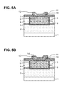
- FIGS. 5A and 5B illustrate cross-sectional views schematically illustrating a fourth process of the method of manufacturing the semiconductor device according to example 1 of the present invention.
- FIG. 6 is a partial cross-sectional view schematically illustrating a configuration of a semiconductor device according to example 2 of the present invention.
- FIGS. 7A, 7B and 7C illustrate cross-sectional views schematically illustrating a first process of a method of manufacturing the semiconductor device according to example 2 of the present invention.
- FIGS. 8A, 8B and 8C illustrate cross-sectional views schematically illustrating a second process of the method of manufacturing the semiconductor device according to example 2 of the present invention.
- FIGS. 9A and 9B illustrate cross-sectional views schematically illustrating a third process of the method of manufacturing the semiconductor device according to example 2 of the present invention.
- FIGS. 10A and 10B illustrate cross-sectional views schematically illustrating a fourth process of the method of manufacturing the semiconductor device according to example 2 of the present invention.
- FIG. 11 is a partial cross-sectional view schematically illustrating a configuration of a semiconductor device according to example 3 of the present invention.
- FIG. 12 is a partial cross-sectional view schematically illustrating a configuration of a semiconductor device according to example 4 of the present invention.
- FIG. 13 is a partial cross-sectional view schematically illustrating a configuration of a semiconductor device according to example 5 of the present invention.
- FIG. 14 is a partial cross-sectional view schematically illustrating a configuration of a semiconductor device according to example 6 of the present invention.
- FIG. 15 is an enlarged sectional view of a region R in FIG. 14 schematically illustrating a configuration of the semiconductor device according to example 6 of the present invention.
- FIG. 16 is a partial cross-sectional view schematically illustrating a variation of a configuration of the semiconductor device according to example 6 of the present invention.
- FIG. 17 illustrates resistance change characteristics of a variable resistance element in a semiconductor device according to example 7 of the present invention.
- a semiconductor device comprises: a semiconductor substrate ( 1 in FIG. 1 ); a multilevel wiring layer structure ( 2 - 7 and 15 - 21 in FIG. 1 ) on the semiconductor substrate ( 1 in FIG. 1 ); and a variable resistance element ( 22 in FIG. 1 ) in the multilevel wiring layer structure ( 2 - 7 and 15 - 21 in FIG. 1 ), wherein the variable resistance element ( 22 in FIG. 1 ) comprises a variable resistance element film ( 9 in FIG. 1 ) whose resistance changes between a top electrode ( 10 , 11 in FIG. 1 ) and a bottom electrode ( 5 in FIG. 1 ), wherein the multilevel wiring layer structure ( 2 - 7 and 15 - 21 in FIG.
- FIG. 1 comprises at least a wiring ( 5 in FIG. 1 ) electrically connected to the bottom electrode ( 5 in FIG. 1 ) and a plug ( 19 in FIG. 1 ) electrically connected to the top electrode ( 10 , 11 in FIG. 1 ), and wherein the wiring ( 5 in FIG. 1 ) also serves as the bottom electrode ( 5 in FIG. 1 ).
- variable resistance element film have a bottom surface at a periphery of a connection portion between the wiring and the variable resistance element film and that the bottom surface be set at an angle of 85 degrees or less with respect to a top surface of the wiring.
- an insulating barrier film be arranged between the bottom electrode and the variable resistance element film, that the insulating barrier film have an opening, and that the variable resistance element film be in contact with the bottom electrode in the opening.
- the opening have a tapered wall surface and have a wider diameter at a portion farther from the wiring, that the tapered surface be set at an angle of 85 degrees or less with respect to a top surface of the wiring, and that the variable resistance element film be arranged so that a periphery of a connection portion between the wiring and the variable resistance element film is at least arranged on the tapered surface.
- an area of a region where the plug and the top electrode are connected be smaller than an area of a region where the variable resistance element film and the wiring are connected.
- a region where the plug and the top electrode are connected be arranged in a region different from a region where the variable resistance element film and the wiring are connected
- the wiring be in contact with the variable resistance element film.
- the wiring be made of copper.
- the wiring be alloyed with Al or that a surface of the wiring be converted into silicide or nitride.
- variable resistance element film be an oxide including Ta or TaSi.
- variable resistance element film have a laminate structure in which Ta 2 O 5 and TaSiO are stacked in this order from bottom to top.
- the top electrode have a structure in which a first top electrode and a second top electrode are stacked in this order on the variable resistance element film, that the first top electrode comprise a metal material having a smaller absolute value in oxidation free energy than that of a metal component of the variable resistance element film, and that the second top electrode be in contact with the plug.
- the first top electrode be made of Pt, Ru, or oxide thereof.
- the second top electrode be made of Ti, Ta, W, or nitride thereof.
- the semiconductor device comprise a second bottom electrode arranged between the wiring and the variable resistance element film and having diffusion barrier properties for a metal of the wiring.
- the second bottom electrode be an electrode having a laminate structure of two layers and that one of the layers that is on the variable resistance element film be made of a material identical to that of the first top electrode.
- the second bottom electrode be an electrode in which TaN and Ru are stacked in this order on the wiring.
- the semiconductor device comprise a second variable resistance element film arranged between the variable resistance element film and the top electrode and made of a metal oxide having a larger absolute value in oxidation free energy than that of a metal component of the variable resistance element film.
- the second variable resistance element film be made of oxide of Ti or Ni.
- a hard mask film be arranged on the top electrode and that a multilayer (laminate) body of the hard mask film, the top electrode, and the variable resistance element film have top and side surfaces covered by a protective insulating film.
- the protective insulating film be in contact with the insulating barrier film at a periphery of the multilayer (laminate) body of the hard mask film, the top electrode, and the variable resistance element film and that the plug extend in a prepared hole formed in the protective insulating film and the hard mask film and be electrically connected to the top electrode.
- a hard mask film be arranged on the top electrode and that a second hard mask film made of a material different from that of the hard mask film be arranged on the hard mask film.
- a multilayer (laminate) body of the second hard mask film, the hard mask film, the top electrode, and the variable resistance element film have a side surface covered by a protective insulating film and that the protective insulating film be in contact with the insulating barrier film at a periphery of the multilayer (laminate) body of the second hard mask film, the hard mask film, the top electrode, and the variable resistance element film.
- the plug extend in a prepared hole formed in the second hard mask film and the hard mask film and be electrically connected to the top electrode.
- a multilayer (laminate) body of the second hard mask film, the hard mask film, the top electrode, and the variable resistance element film have top and side surfaces covered by a protective insulating film and that the protective insulating film be in contact with the insulating barrier film at a periphery of the multilayer (laminate) body of the second hard mask film, the hard mask film, the top electrode, and the variable resistance element film.
- the plug extend in a prepared hole formed in the protective insulating film, the second hard mask film, and the hard mask film and be electrically connected to the top electrode via a barrier metal.
- the protective insulating film be made of a material identical to that of the hard mask film and the insulating barrier film.
- the semiconductor device comprise a second variable resistance element that is formed in a layer identical to or different from that of the variable resistance element in the multilevel wiring layer structure and that comprises a variable resistance element film whose resistance changes between a top electrode and a bottom electrode.
- the multilevel wiring layer structure comprise at least a second wiring electrically connected to the bottom electrode of the second variable resistance element and a second plug electrically connected to the top electrode of the second variable resistance element and that the second wiring also serve as the bottom electrode of the second variable resistance element.
- the second wiring be integrated with the plug.
- variable resistance element film be made of oxide containing Ni.
- the top electrode have a structure in which a first top electrode and a second top electrode are stacked in this order on the variable resistance element film, that the first top electrode be made of Ru, and that the second bottom electrode be an electrode in which TaN and Ru are stacked in this order on the wiring.
- a method of manufacturing a semiconductor device comprising a variable resistance element in a multilevel wiring layer structure on a semiconductor substrate according to exemplary embodiment 2 of the present invention comprises the steps of: forming a variable resistance element film and a top electrode in this order on a wiring ( FIGS. 3C and 4A ); and forming a plug on the top electrode ( FIG. 1 ).
- the method comprise, prior to the step of forming the variable resistance element film and the top electrode, the steps of: forming an insulating barrier film on the wiring; forming a hard mask having an opening pattern on the insulating barrier film; using the hard mask as a mask and carrying out reactive dry etching on the insulating barrier film exposed in the opening pattern to form an opening in the insulating barrier film, the opening extending to the wiring, having a tapered wall surface, and having a wider diameter at a portion farther from the wiring; and using an inactive gas and carrying RF etching to adjust the tapered surface of the opening to a desired angle.
- the variable resistance element film be formed also on the tapered surface.
- the hard mask have a multilayer (laminate) structure in which SiN and SiO 2 are stacked in this order on the insulating barrier film.
- a gas containing fluorocarbon be used as etching gas in the reactive dry etching.
- the inactive gas be He or Ar.
- the method comprise a process of emitting SiH 4 gas to the wiring, prior to the step of forming the variable resistance element film and the top electrode.
- a plasma treatment be carried out on the wiring by using NH 3 or N 2 gas, prior to the step of forming the variable resistance element film and the top electrode.
- a second bottom electrode, the variable resistance element film, a second variable resistance element film, and the top electrode be formed in this order on a bottom electrode, that the second bottom electrode have diffusion barrier properties for a metal of the bottom electrode, and that the second variable resistance element film be made of a metal oxide having a larger absolute value in oxidation free energy than that of a metal component of the variable resistance element film.
- the method comprise, after the step of forming the variable resistance element film and the top electrode and before the step of forming the plug, the steps of forming a protective insulating film on the insulating barrier film including a multilayer (laminate) body of the hard mask film, the top electrode, and the variable resistance element film and forming a prepared hole extending to the top electrode in the protective insulating film and the hard mask film, and that a second hard mask film be made of a material different from the hard mask film.
- the method comprise, after the step of forming the variable resistance element film and the top electrode and before the step of forming a barrier metal, the steps of forming a protective insulating film on the insulating barrier film including a multilayer (laminate) body of the second hard mask film, the hard mask film, the top electrode, and the variable resistance element film and forming a prepared hole extending to the top electrode in the protective insulating film, the second hard mask film and the hard mask film, and that the second hard mask film be made of a material different from that of the hard mask film.
- the method comprise, after the step of forming the variable resistance element film and the top electrode and before the step of forming a barrier metal, the steps of forming a protective insulating film on the insulating barrier film including a multilayer (laminate) body of the second hard mask film, the hard mask film, the top electrode, and the variable resistance element film, polishing the protective insulating film and the second hard mask film for planarization until the second hard mask film assumes a predetermined thickness, and forming a prepared hole extending to the top electrode in the second hard mask film and the hard mask film, and that the second hard mask film be made of a material different from that of the hard mask film.
- the protective insulating film be made of a material identical to that of the hard mask film and the insulating barrier film.
- FIG. 1 is a partial cross-sectional view schematically illustrating a configuration of the semiconductor device according to example 1 of the present invention.
- the semiconductor device according to example 1 includes a variable resistance element 22 in a multilevel wiring layer structure on a semiconductor substrate 1 .
- a second wiring 18 is embedded in a wiring trench formed in the interlayer insulating film 17 and the etching stopper film 16 .
- a plug 19 is embedded in a prepared hole formed in the interlayer insulating film 15 , the protective insulating film 14 , and a hard mask film 12 .
- the second wiring 18 and the plug 19 are integrally formed, and side and bottom surfaces of the second wiring and the plug 19 are covered by a barrier metal 20 .
- the first wiring 5 serving as a bottom electrode is formed at an opening formed in the insulating barrier film 7 , and the variable resistance element 22 formed by stacking a variable resistance element film 9 , a first top electrode 10 , and a second top electrode 11 in this order is formed on the side surface of the opening in the insulating barrier film 7 and on the insulating barrier film 7 .
- the hard mask film 12 is formed on the second top electrode 11 , and a multilayer (laminate) body of the variable resistance element film 9 , the first top electrode 10 , the second top electrode 11 , and the hard mask film 12 have top and side surfaces covered by the protective insulating film 14 .
- the first wiring 5 is used as a bottom electrode of the variable resistance element 22 , namely, since the first wiring 5 also serves as a bottom electrode of the variable resistance element 22 , the number of processing steps can be simplified and the electrode resistance can be reduced.
- the variable resistance element can be mounted. As a result, reduction in both the resistance and the cost of the element can be achieved.
- the variable resistance element 22 is a variable-resistance-type nonvolatile element and can be formed as a switching element using metal ion movement and electrochemical reaction in an ion conductor, for example.
- the variable resistance element 22 includes the variable resistance element film 9 arranged between the first wiring 5 serving as a bottom electrode and the top electrodes 10 and electrically connected to the plug 19 . Based on the variable resistance element 22 , the variable resistance element film 9 and the first wiring 5 are in direct contact with each other at the opening formed in the insulating barrier film 7 , and the plug 19 and the second top electrode 11 are electrically connected to each other via the barrier metal 20 on the second top electrode 11 .
- the on/off control of the variable resistance element 22 is executed by application of a voltage or a current.
- the on/off control is executed.
- the second top electrode 11 and the barrier metal 20 are made of an identical material. In this way, since the barrier metal 20 of the plug 19 is integrated with the second top electrode 11 of the variable resistance element 22 , the contact resistance can be reduced. In addition, improvement in adherence can realize improvement in reliability.
- Semiconductor elements are formed on the semiconductor substrate 1 .
- a silicon substrate, a single-crystal substrate, an SOI (Silicon on Insulator) substrate, a TFT (Thin Film Transistor) substrate, or a liquid crystal manufacture substrate can be used as the semiconductor substrate 1 .
- the interlayer insulating film 2 is formed on the semiconductor substrate 1 .
- a silicon oxide film or a low-dielectric-constant film (SiOCH film, for example) having a relative dielectric constant lower than that of a silicon oxide film can be used as the interlayer insulating film 2 .
- the interlayer insulating film 2 may be formed by stacking a plurality of insulating films.
- the barrier insulating film 3 is arranged between the interlayer insulating films 2 and 4 and has barrier properties.
- the barrier insulating film 3 serves as an etching stop layer when a wiring trench for the first wiring 5 is processed.
- a SiN film, a SiC film, a SiCN film, or the like can be used as the barrier insulating film 3 .
- a wiring trench for embedding the first wiring 5 is formed in the barrier insulating film 3 .
- the first wiring 5 is embedded in the wiring trench via the barrier metal 6 .
- the barrier insulating film 3 may be deleted, depending on selection of etching conditions of the wiring trench.
- the interlayer insulating film 4 is formed on the barrier insulating film 3 .
- a silicon oxide film or a low-dielectric-constant film (SiOCH film, for example) having a relative dielectric constant lower than that of a silicon oxide film can be used as the interlayer insulating film 4 .
- the interlayer insulating film 4 may be formed by stacking a plurality of insulating films.
- a wiring trench for embedding the first wiring 5 is formed in the barrier insulating film 4 .
- the first wiring 5 is embedded in the wiring trench via the barrier metal 6 .
- the first wiring 5 is embedded in the wiring trench formed in the interlayer insulating film 4 and the barrier insulating film 3 via the barrier metal 6 .
- the first wiring 5 also serves as a bottom electrode of the variable resistance element 22 and is in direct contact with the variable resistance element film 9 .
- An electrode layer or the like may be inserted between the first wiring 5 and the variable resistance element film 9 .
- the electrode layer and the variable resistance element film 9 are deposited in continuous processes and processed in continuous processes.
- the bottom portion of the variable resistance element film 9 is not connected to a lower-layer wiring via a contact plug.
- the first wiring 5 is made of a metal that enables diffusion or ion conduction in the variable resistance element film 9 .
- Cu or the like can be used.
- the first wiring 5 may be alloyed with Al or converted into silicide or nitride. A surface of the first wiring 5 may be converted into silicide or nitride.
- the barrier metal 6 is a conductive film having barrier properties.
- the barrier metal 6 covers the side and bottom surfaces of the wiring, to prevent the metal of the first wiring 5 from diffusing into the interlayer insulating film 4 and lower layers.
- a high-melting-point metal such as tantalum (Ta), tantalum nitride (TaN), titanium nitride (TiN), or tungsten carbonitride (WCN), nitride of such metal, or layers of such films can be used as the barrier metal 6 .
- the insulating barrier film 7 is formed on the interlayer insulating film 4 including the first wiring 5 and serves to prevent oxidation of the metal (for example, Cu) of the first wiring 5 and diffusion of the metal of the first wiring 5 into the interlayer insulating film 15 .
- the insulating barrier film 7 serves as an etching stop layer when the top electrodes 11 and 10 and the variable resistance element film 9 are processed.
- a SiC film, a SiCN film, a SiN film, or a multilayer (laminate) structure of such films can be used as the insulating barrier film 7 . It is preferable that the insulating barrier film 7 be made of a material identical to that of the protective insulating film 14 and the hard mask film 12 .
- the insulating barrier film 7 has an opening on the first wiring 5 .
- the first wiring 5 and the variable resistance element film 9 are in contact with each other at the opening in the insulating barrier film 7 .
- the opening in the insulating barrier film 7 is formed within an area of the first wiring 5 .
- the variable resistance element 22 can be formed on a surface of the first wiring 5 having a small irregularity.
- the wall surface of the opening in the insulating barrier film 7 is a tapered surface.
- the opening has a wider diameter at a portion farther from the first wiring 5 .
- the tapered surface of the opening in the insulating barrier film 7 is set at 85 degrees or less with respect to the top surface of the first wiring 5 . In this way, electric field concentration at the periphery of the connection portion between the first wiring 5 and the variable resistance element film 9 (around the periphery of the opening in the insulating barrier film 7 ) is reduced. Thus, the insulation resistance can be improved.
- the variable resistance element film 9 is a film whose resistance changes.
- An arbitrary material can be used as the variable resistance element film 9 , as long as the resistance thereof changes depending on actions (diffusion, ion transmission, etc.) of the metal of the first wiring 5 (bottom electrode). If the resistance of the variable resistance element 22 is changed by precipitation of metal ions, a film that enables ion conduction is used.
- an oxide insulating film including Ta such as Ta 2 O 5 or TaSiO, may be used.
- the variable resistance element film 9 may have a multilayer (laminate) structure in which Ta 2 O 5 (lower layer) and TaSiO (upper layer) are stacked in this order from bottom to top.
- variable resistance element film 9 when the variable resistance element film 9 is used as an ion conducting layer, a bridge of metal ions (copper ions, for example) formed in the ion conducting layer during a low resistance (ON) can be cut off by the Ta 2 O 5 layer. Thus, since the metal ions can be easily collected during OFF, the switching characteristics can be improved.
- the variable resistance element film 9 is formed on the first wiring 5 , on the tapered surface of the opening of the insulating barrier film 7 , and on the insulating barrier film 7 .
- the periphery of the connection portion between the first wiring 5 and the variable resistance element film 9 is arranged at least along the tapered surface of the opening in the insulating barrier film 7 .
- the bottom surface of the periphery of the connection portion between the first wiring 5 and the variable resistance element film 9 is set at an angle of 85 degrees or less with respect to the top surface of the first wiring 5 .
- the first top electrode 10 is an electrode disposed at a lower side of the top electrodes of the variable resistance element 22 and is in direct contact with the variable resistance element film 9 . It is preferable that the first top electrode 10 be made of a metal that is not easily ionized and that does not easily enable diffusion or ion conduction in the variable resistance element film 9 , as compared with the metal of the first wiring 5 . In addition, it is preferable that the first top electrode 10 be made of a metal material having a smaller absolute value in oxidation free energy than that of the metal component (Ta) of the variable resistance element film 9 . For example, Pt, Ru, or the like can be used as the first top electrode 10 . Alternatively, oxygen may be added to the first top electrode 10 including a metal material such as Pt or Ru as a primary component. Alternatively, the first top electrode 10 may have a multilayer (laminate) structure including a layer in which oxygen is added.
- the second top electrode 11 is an upper one of the top electrodes of the variable resistance element 22 and is formed on the first top electrode 10 .
- the second top electrode 11 serves to protect the first top electrode 10 . Namely, since the second top electrode 11 protects the first top electrode 10 , damage to the first top electrode 10 during processing can be suppressed. Consequently, switching characteristics of the variable resistance element 22 can be maintained.
- Ta, Ti, W, or a nitride thereof can be used as the second top electrode 11 . It is preferable that the second top electrode 11 be made of a material identical to that of the barrier metal 20 .
- the second top electrode 11 is electrically connected to the plug 19 via the barrier metal 20 .
- a diameter R 2 (or the area) of the region where the second top electrode 11 and the plug 19 (the barrier metal 20 to be exact) are in contact with each other is set to be smaller than a diameter R 1 (or the area) of the region where the first wiring 5 and the variable resistance element film 9 are in contact with each other.
- the hard mask film 12 is a film used as a hard mask when etching the second top electrode 11 , the first top electrode 10 , and the variable resistance element film 9 .
- a SiN film or the like can be used as the hard mask film 12 .
- the hard mask film 12 be made of a material identical to that of the protective insulating film 14 and the insulating barrier film 7 . Namely, by covering the variable resistance element 22 with an identical material, a uniform material interface can be obtained. Therefore, ingress of moisture or the like from the outside can be prevented, and removal of any of the films 7 , 12 , and 14 from the variable resistance element 22 can be prevented.
- the protective insulating film 14 serves to prevent damage to the variable resistance element 22 and removal of oxygen from the variable resistance element film 9 .
- a SiN film, a SiCN film, or the like can be used as the protective insulating film 14 .
- the protective insulating film 14 be made of a material identical to that of the hard mask film 12 and the insulating barrier film 7 . If made of an identical material, the protective insulating film 14 can be integrated with the insulating barrier film 7 and the hard mask film 12 . Thus, since adherence of the interface is improved, the variable resistance element 22 can be protected more securely.
- the interlayer insulating film 15 is formed on the protective insulating film 14 .
- a silicon oxide film, a SiOC film, or a low-dielectric-constant film (SiOCH film, for example) having a relative dielectric constant lower than that of a silicon oxide film can be used as the interlayer insulating film 15 .
- the interlayer insulating film 15 may be formed by stacking a plurality of insulating films.
- the interlayer insulating film 15 may be made of a material identical to that of the interlayer insulating film 17 .
- a prepared hole for embedding the plug 19 is formed in the interlayer insulating film 15 .
- the plug 19 is embedded in the prepared hole via the barrier metal 20 .
- the etching stopper film 16 is an insulating film arranged between the interlayer insulating films 15 and 17 .
- the etching stopper film 16 serves as an etching stop layer when a wiring trench for the second wiring 18 is processed.
- a SiN film, a SiC film, a SiCN film, or the like can be used as the etching stopper film 16 .
- a wiring trench for embedding the second wiring 18 is formed in the etching stopper film 16 .
- the second wiring 18 is embedded in the wiring trench via barrier metal 20 .
- the etching stopper film 16 may be deleted, depending on selection of etching conditions of the wiring trench.
- the interlayer insulating film 17 is formed on the etching stopper film 16 .
- a silicon oxide film, a SiOC film, or a low dielectric constant film (SiOCH film, for example) having a relative dielectric constant lower than that of a silicon oxide film can be used as the interlayer insulating film 17 .
- the interlayer insulating film 17 may be formed by stacking a plurality of insulating films.
- the interlayer insulating film 17 may be made of a material identical to that of the interlayer insulating film 15 .
- a wiring trench for embedding the second wiring 18 is formed in the interlayer insulating film 17 .
- the second wiring 18 is embedded in the wiring trench via the barrier metal 20 .
- the second wiring 18 is embedded in the wiring trench formed in the interlayer insulating film 17 and the etching stopper film 16 via the barrier metal 20 .
- the second wiring 18 is integrated with the plug 19 .
- the plug 19 is embedded in the prepared hole formed in the interlayer insulating film 15 , the protective insulating film 14 , and the hard mask film 12 via the barrier metal 20 .
- the plug 19 is electrically connected to the second top electrode 11 via the barrier metal 20 .
- Cu can be used as the second wiring 18 and the plug 19 .
- the diameter R 2 (or the area) of the region where the plug 19 (the barrier metal 20 , to be exact) and the second top electrode 11 are in contact with each other is set to be smaller than the diameter R 1 (or the area) of the region where the first wiring 5 and the variable resistance element film 9 are in contact with each other.
- the barrier metal 20 is a conductive film that has barrier properties and covers the side and bottom surfaces of the second wiring 18 and the plug 19 , to prevent the metal of the second wiring 18 (including the plug 19 ) from diffusing into the interlayer insulating films 15 and 17 and lower layers.
- a high-melting-point metal such as tantalum (Ta), tantalum nitride (TaN), titanium nitride (TiN), or tungsten carbonitride (WCN), nitride of such metal, or laminate layers of such films can be used as the barrier metal 20 .
- the barrier metal 20 be made of a material identical to that of the second top electrode 11 .
- the barrier metal 20 has a multilayer (laminate) structure of TaN (lower layer)/Ta (upper layer)
- the second top electrode 11 be made of TaN used as the lower layer material.
- the barrier metal 20 is made of Ti (lower layer)/Ru (upper layer)
- the lower layer material Ti be used as the second top electrode 11 .
- the barrier insulating film 21 is formed on the interlayer insulating film 17 including the second wiring 18 and serves to prevent oxidation of the metal (Cu, for example) of the second wiring 18 and diffusion of the metal of the second wiring 18 into upper layers.
- a SiC film, a SiCN film, a SiN film, or a multilayer (laminate) structure of such films can be used as the barrier insulating film 21 .
- FIGS. 2A to 5B are cross-sectional views schematically illustrating processes of a method of manufacturing the semiconductor device according to example 1 of the present invention.
- the interlayer insulating film 2 (a silicon oxide film having a film thickness of 300 nm, for example) is deposited on the semiconductor substrate 1 (a substrate on which semiconductor elements are formed, for example).
- the barrier insulating film 3 (a SiN film having a film thickness of 50 nm, for example) is deposited on the interlayer insulating film 2 .
- the interlayer insulating film 4 (a silicon oxide film having a film thickness of 300 nm, for example) is deposited on the barrier insulating film 3 .
- a lithography method including photoresist formation, dry etching, and photoresist removal
- a wiring trench is formed in the interlayer insulating film 4 and the barrier insulating film 3 .
- the first wiring 5 (copper, for example) is embedded in the wiring trench via the barrier metal 6 (TaN/Ta having a film thickness of 5 nm/5 nm, for example) (see step A 1 in FIG. 2A ).
- the interlayer insulating films 2 and 4 can be formed by a plasma CVD method.
- a plasma CVD (Chemical Vapor Deposition) method for example, a vaporized gas or liquid material is continuously supplied into a reaction chamber under a reduced pressure. Molecules of the material are excited because of the plasma energy.
- a continuous film is formed on a substrate by a gas phase reaction, a substrate surface reaction, or the like.
- the first wiring 5 can be formed by: forming the barrier metal 6 (layers of films TaN/Ta, for example) by a PVD method; forming a Cu seed by a PVD method; embedding copper in the wiring trench by an electrolytic plating method; executing a heat treatment at a temperature of 200° C. or more; and removing excess copper that is present outside the wiring trench by a CMP method.
- the copper wiring can be formed by such series of procedures, a general method known in the art can be used.
- the insulating barrier film 7 (a SiN film having a film thickness of 50 nm, for example) is formed on the interlayer insulating film 4 including the first wiring 5 (see step A 2 in FIG. 2B ).
- the insulating barrier film 7 can be formed by a plasma CVD method. It is preferable that the insulating barrier film 7 have a film thickness of approximately, 10 nm to 50 nm.
- the hard mask film 8 (a silicon oxide film, for example) is formed on the insulating barrier film 7 (see step A 3 in FIG. 2C ). It is preferable that the hard mask film 8 be made of a material different from that of the insulating barrier film 7 , in order to maintain large etching selectivity during a dry etching process.
- the hard mask film 8 may be an insulating film or a conducting film.
- a silicon oxide film, a silicon nitride film, TiN, Ti, Ta, TaN or the like can be used as the hard mask film 8 .
- a multilayer (laminate) body of SiN/SiO 2 may be used.
- a photoresist (not illustrated) is used on the hard mask film 8 to pattern an opening.
- dry etching is executed to form an opening pattern in the hard mask film 8 .
- the photoresist is stripped by oxygen plasma ashing or the like (see step A 4 in FIG. 3A ).
- the dry etching does not necessarily stop on the top surface of the insulating barrier film 7 .
- An inner portion of the insulating barrier film 7 may also be dry-etched.
- the insulating barrier film 7 exposed in the opening in the hard mask film 8 is etched back (dry etching).
- the first wiring 5 is exposed in the opening in the insulating barrier film 7 .
- an amine-based stripping solution or the like and executing an organic stripping process oxidized copper formed on the exposed surface of the first wiring 5 and etching byproducts or the like generated during the etch-back process are removed (see step A 5 in FIG. 3B ).
- step A 5 it is preferable that the hard mask film ( 8 in FIG. 3A ) be completely removed during the etch-back process. However, if the hard mask film is an insulating material, the hard mask film may be allowed to remain.
- the opening in the insulating barrier film 7 has a circular shape and has a diameter of 30 nm to 500 nm.
- step A 5 when the insulating barrier film 7 is etched back, reactive dry etching can be used. In this way, the wall surface of the opening in the insulating barrier film 7 can be formed to be a tapered surface.
- reactive dry etching a fluorocarbon-containing gas can be used as the etching gas.
- the oxide on the surface of the first wiring 5 is removed by RF (Radio Frequency) etching using an inactive gas, and the tapered surface of the opening in the insulating barrier film 7 is adjusted to have a desired taper angle (85 degrees or less) (see step A 6 in FIG. 3B ).
- RF Radio Frequency
- the taper angle can be adjusted without carrying out excess RF etching.
- Either He or Ar can be used as the inactive gas.
- variable resistance element film ( 9 in FIG. 3C ) is an oxide insulator, regarding embedment properties inside the opening in the insulating barrier film 7 , it is more difficult to control the directivity. As a result, it is difficult to maintain uniform coverage, compared with conventional metal-based sputtering techniques.
- the desired taper angle ⁇ 1 needs to be formed, while preventing damage (oxidation) to the first wiring 5 present as a lower layer.
- variable resistance element film 9 (Ta 2 O 5 having a film thickness of 15 nm, for example) is deposited on the insulating barrier film 7 including the first wiring 5 (see step A 7 in FIG. 3C ).
- the variable resistance element film 9 can be formed by using a PVD method or a CVD method.
- a heat treatment be executed at a temperature of approximately 250° C. to 350° C. under a reduced pressure for degassing. Care is required so as not to oxidize the copper surface again.
- the heat treatment needs to be executed under vacuum or in a nitrogen atmosphere, for example.
- a SiH 4 gas may be emitted to the first wiring 5 exposed in the opening in the insulating barrier film 7 at approximately 350° C. under a reduced pressure.
- the surface of the first wiring 5 can be converted into silicide and diffusion of the metal (copper, for example) of the first wiring 5 during processing can be suppressed.
- approximately 1 atm % of A 1 may be added to the Cu seed layer. In this way, the A 1 can be diffused inside the Cu during annealing of the Cu electrolytic plating film, and as a result, the copper can be alloyed.
- Such conversion of copper into an alloy or a silicide is effective in inhibiting movement of the copper that comes into contact with the variable resistance element film 9 (stabilization of the copper), whereby reliability of the semiconductor device can be improved when operated at a high temperature.
- a plasma treatment (nitriding treatment) may be executed on the first wiring 5 exposed in the opening in the insulating barrier film 7 .
- oxidation of the first wiring 5 copper
- thermal diffusion material transfer
- step A 7 instead of an ion conducting layer, if a transition metal oxide (TiO, NiO, or the like, for example) is used as the variable resistance element film 9 , prior to the deposition of the variable resistance element film 9 , a second bottom electrode (not illustrated; corresponding to 5 c in FIG. 13 ) may be formed.
- a transition metal oxide TiO, NiO, or the like, for example
- Ti, TiN, W, WN, Ta, TaN, Ru, RuO x , or the like can be used as the second bottom electrode.
- a multilayer (laminate) structure of such elements (TaN (lower layer)/Ru (upper layer), for example) may be used.
- the variable resistance element 9 is formed in via interlayer insulating films.
- the total film thickness of the multilayer (laminate) structure needs to be smaller than that of the insulating barrier film 7 . It is preferable that the total film thickness of the multilayer (laminate) structure be 10 nm or less.
- the first top electrode 10 (Ru having a film thickness of 10 nm, for example) and the second top electrode 11 (Ta having a film thickness of 150 nm, for example) are formed in this order on the variable resistance element film 9 (see step A 8 in FIG. 4A ).
- the hard mask film 12 (a SiN film having a film thickness of 30 nm, for example) and the hard mask film 13 (a SiO 2 film having a film thickness of 200 nm, for example) are stacked in this order on the second top electrode 11 (see step A 9 in FIG. 4B ).
- the hard mask film 12 and the hard mask film 13 can be formed by using a plasma CVD method.
- a general plasma CVD method known in the art can be used to form the hard mask films 12 and 13 .
- the hard mask film 12 and the hard mask film 13 be films of different types.
- a SiN film and a SiO 2 film can be formed as the hard mask film 12 and the hard mask film 13 , respectively.
- the hard mask film 12 be made of a material identical to that of the protective insulating film 14 to be described later and the insulating barrier film 7 . Namely, by covering the variable resistance element with an identical material, a uniform material interface can be obtained.
- the hard mask film 12 can be formed by a plasma CVD method, prior to the film formation, the pressure needs to be maintained at a reduced level in a reaction chamber. This process may cause removal of oxygen from the variable resistance element film 9 and the deficiency of oxygen may increase the leakage current from the ion conducting layer, counted as a problem.
- the film formation temperature needs to be 350° C. or less. It is preferable that the temperature be 250° C. or less.
- no reducing gas be used.
- a SiN film etc. be formed by using a mixed gas of SiH 4 N 2 in high-density plasma at a substrate temperature of 200° C.
- a photoresist (not illustrated) is formed on the hard mask film 13 .
- the hard mask film 13 is dry-etched until the hard mask film 12 is exposed.
- the photoresist is removed (see step A 10 in FIG. 4C ).
- the hard mask film ( 13 in FIG. 4C ) As a mask, the hard mask film 12 , the second top electrode 11 , the first top electrode 10 , and the variable resistance element film 9 are dry-etched continuously (see step A 11 in FIG. 5A ). In this process, while it is preferable that the hard mask film ( 13 in FIG. 4C ) be completely removed during the etch-back process, the hard mask film may be allowed to remain.
- step A 11 for example, if the second top electrode 11 is made of Ta, processing can be executed by a Cl 2 -based RIE. If the first top electrode 10 is made of Ru, processing can be executed by RIE using a mixed gas of Cl 2 /O 2 . In addition, during etching of the variable resistance element film 9 , when the insulating barrier film 7 as a lower surface is reached, the dry etching needs to be stopped.
- variable resistance element film 9 is an oxide including Ta and the insulating barrier film 7 is a SiN film or a SiCN film
- the films can be processed by RIE.
- RIE hard mask RIE method
- the variable resistance element portion can be processed, without causing the variable resistance element portion to be exposed to oxygen plasma ashing to remove the resist.
- an oxidation treatment is carried out by oxygen plasma after the process, the oxidation plasma treatment can be carried out irrespective of the stripping time of the resist.
- the protective insulating film 14 (a SiN film of 30 nm, for example) is deposited on the insulating barrier film 7 including the hard mask film 12 , the second top electrode 11 , the first top electrode 10 , and the variable resistance element film 9 (see step A 12 in FIG. 5B ).
- step A 12 while the protective insulating film 14 can be formed by a plasma CVD method, prior to the film formation, the pressure needs to be maintained at a reduced level in a reaction chamber. This process may cause removal of oxygen from the side surface of the variable resistance element film 9 and increase the leakage current from the ion conducting layer, counted as a problem. To prevent such problem, it is preferable that the film formation temperature of the protective insulating film 14 be 250° C. or less. In addition, since the material is exposed to a film formation gas under a reduced pressure prior to the film formation, it is preferable that no reducing gas be used. For example, it is preferable that a SiN film be formed by using a mixed gas of SiH 4 /N 2 in high-density plasma at a substrate temperature of 200° C.
- the interlayer insulating film 15 (a silicon oxide film, for example), the etching stopper film 16 (a SiN film, for example), and the interlayer insulating film 17 (a silicon oxide film, for example) are deposited in this order on the protective insulating film 14 .
- a Wiring trench for the second wiring 18 and a prepared hole for the plug 19 are formed.
- the second wiring 18 (Cu, for example) and the plug 19 (Cu, for example) are simultaneously formed in the wiring trench and the prepared hole, respectively, via the barrier metal 20 (TaN/Ta, for example).
- the insulating barrier film 21 (a SiN film, for example) is deposited on the interlayer insulating film 17 including the second wiring 18 (see step A 13 in FIG. 1 ).
- the second wiring 18 can be formed by a process similar to that used to form the lower layer wirings.
- the barrier metal 20 is made of a material identical to that of the second top electrode 11 . In this way, the contact resistance between the plug 19 and the second top electrode 11 can be reduced. As a result, element performance can be improved (reduction in resistance of the variable resistance element 22 during ON).
- the interlayer insulating film 15 and the interlayer insulating film 17 can be formed by a plasma CVD method.
- the interlayer insulating film 15 may be thickly deposited first.
- the interlayer insulating film 15 can be formed to have a desired film thickness.
- the first wiring 5 is used as a bottom electrode of the variable resistance element 22 .
- the variable resistance element 22 can have a smaller size.
- the density can be increased and the number of processing steps can be simplified.
- the variable resistance element 22 can be mounted. At the same time, costs of the device can be reduced.
- the wall surface of the opening in the insulating barrier film 7 is formed to have a taper angle of 85 degrees or less, electric field concentration at the periphery of the connection portion between the first wiring 5 and the variable resistance element film 9 (around the periphery of the opening in the insulating barrier film 7 ) is reduced. Thus, the insulation resistance can be improved. Furthermore, since the variable resistance element 22 can also be mounted in a most-advanced device comprising copper wirings, performance of the device can be improved.
- FIG. 6 is a partial cross-sectional view schematically illustrating a configuration of the semiconductor device according to example 2 of the present invention.
- the top and side surfaces of the multilayer (laminate) body of the variable resistance element film ( 9 in FIG. 1 ), the first top electrode ( 10 in FIG. 1 ), the second top electrode ( 11 in FIG. 1 ), and the hard mask film ( 12 in FIG. 1 ) is covered by the protective insulating film ( 14 in FIG. 1 ).
- a thick hard mask film 23 is formed on the multilayer (laminate) body of the variable resistance element film 9 , the first top electrode 10 , the second top electrode 11 , and the hard mask film 12 .
- variable resistance element film 9 the side surfaces of the variable resistance element film 9 , the first top electrode 10 , the second top electrode 11 , the hard mask film 12 , and the hard mask film 23 are covered by a protective insulating film 24 . While not formed on the hard mask film 23 , the protective insulating film 24 is formed on the insulating barrier film 7 .
- wiring portions ( 5 b , 18 b , 19 b ) that are not electrically connected to a variable resistance element 25 are also illustrated.
- the plug 19 b of the second wiring 18 b is electrically connected to the first wiring 5 b via a barrier metal 20 b .
- Other configurations are the same as those according to example 1.
- a first wiring 5 a is embedded in a wiring trench formed in the interlayer insulating film 4 and the barrier insulating film 3 via a barrier metal 6 a .
- the first wiring 5 a also serves as a bottom electrode of the variable resistance element 25 and is in direct contact with the variable resistance element film 9 .
- An electrode layer or the like may be inserted between the first wiring 5 a and the variable resistance element film 9 .
- the electrode layer and the variable resistance element film 9 are deposited in continuous processes and processed in continuous processes.
- the first wiring 5 a is made of a metal that enables diffusion or ion conduction in the variable resistance element film 9 .
- Cu or the like can be used.
- a surface of the first wiring 5 a may be coated with CuSi.
- the first wiring 5 b is embedded in a wiring trench formed in the interlayer insulating film 4 and the barrier insulating film 3 via a barrier metal 6 b .
- the first wiring 5 b is not connected to the variable resistance element 25 but electrically connected to the plug 19 b via the barrier metal 20 b .
- the first wiring 5 b is made of a material identical to that of the first wiring 5 a . For example, Cu or the like can be used.
- Each of the barrier metals 6 a and 6 b is a conductive film having barrier properties.
- the barrier metals 6 a and 6 b cover the side and bottom surfaces of the respective wirings to prevent the metal of the respective first wirings 5 a and 5 b from diffusing into the interlayer insulating film 4 and lower layers.
- a high-melting-point metal such as tantalum (Ta), tantalum nitride (TaN), titanium nitride (TiN), or tungsten carbonitride (WCN), nitride of such metal, or layers of such films can be used as the barrier metals 6 a and 6 b.
- a second wiring 18 a is embedded in a wiring trench formed in the interlayer insulating film 17 and the etching stopper film 16 via a barrier metal 20 a .
- the second wiring 18 a is integrated with a plug 19 a .
- the plug 19 a is embedded in a prepared hole formed in the hard mask film 23 and the protective insulating film 24 via the barrier metal 20 a .
- the plug 19 a is electrically connected to the second top electrode 11 via the barrier metal 20 a .
- Cu can be used as the second wiring 18 a and the plug 19 a .
- the diameter (or the area) of the region where the plug 19 a (the barrier metal 20 a , to be exact) and the second top electrode 11 are in contact with each other is set to be smaller than the diameter (or the area) of the region where the first wiring 5 and the variable resistance element film 9 are in contact with each other.
- the second wiring 18 b is embedded in a wiring trench formed in the interlayer insulating film 17 and the etching stopper film 16 via the barrier metal 20 b .
- the second wiring 18 b is integrated with the plug 19 b .
- the plug 19 b is embedded in a prepared hole formed in the interlayer insulating film 15 , the protective insulating film 24 , and the insulating barrier film 7 via the barrier metal 20 b .
- the plug 19 b is electrically connected to the first wiring 5 b via the barrier metal 20 b .
- the second wiring 18 b and the plug 19 b are made of a material identical to that of the second wiring 18 a and the plug 19 a . For example, Cu can be used.
- Each of the barrier metals 20 a and 20 b is a conductive film having barrier properties.
- the barrier metals 20 a and 20 b cover the side and bottom surfaces of the second wirings 18 a and 18 b and the plugs 19 a and 19 b , to prevent the metal of the respective second wirings 18 a and 18 b (including the plugs 19 a and 19 b ) from diffusing into the interlayer insulating films 15 and 17 and lower layers.
- the second wirings 18 a and 18 b and the plugs 19 a and 19 b are made of metal elements including Cu as a primary component
- a high-melting-point metal such as tantalum (Ta), tantalum nitride (TaN), titanium nitride (TiN), or tungsten carbonitride (WCN), nitride of such metal, or layers of such films can be used as the barrier metals 20 a and 20 b .
- the barrier metals 20 a and 20 b be made of a material identical to that of the second top electrode 11 .
- each of the barrier metals 20 a and 20 b has a multilayer (laminate) structure of TaN (lower layer)/Ta (upper layer), it is preferable that the second top electrode 11 be made of TaN, which is used as the lower layer material of the barrier metals 20 a and 20 b . If each of the barrier metals 20 a and 20 b is made of Ti (lower layer)/Ru (upper layer), it is preferable that the second top electrode 11 be made of Ti, which is used as the lower layer material of the barrier metals 20 a and 20 b.
- the hard mask film 23 is a film used as a hard mask when etching the hard mask film 12 . It is preferable that the hard mask film 12 and the hard mask film 23 be films of different types. For example, a SiN film and a SiO 2 film can be formed as the hard mask film 12 and the hard mask film 23 , respectively.
- the protective insulating film 24 serves to prevent removal of oxygen from the variable resistance element film 9 without causing damage to the variable resistance element 25 .
- a SiN film, a SiCN film, or the like can be used as the protective insulating film 24 .
- the protective insulating film 24 be made of a material identical to that of the hard mask film 12 and the insulating barrier film 7 . If made of an identical material, the protective insulating film 24 can be integrated with the insulating barrier film 7 and the hard mask film 12 . Thus, adherence of the interface is improved.
- FIGS. 7A to 10B are cross-sectional views schematically illustrating processes of the method of manufacturing the semiconductor device according to example 2 of the present invention.
- the interlayer insulating film 2 (a silicon oxide film having a film thickness of 300 nm, for example) is deposited on the semiconductor substrate 1 (a substrate on which semiconductor elements are formed, for example).
- the barrier insulating film 3 (a SiN film having a film thickness of 50 nm, for example) is deposited on the interlayer insulating film 2 .
- the interlayer insulating film 4 (a silicon oxide film having a film thickness of 300 nm, for example) is deposited on the barrier insulating film 3 .
- wiring trenches are formed in the interlayer insulating film 4 , the barrier insulating film 3 , and the interlayer insulating film 2 .
- the first wirings 5 a and 5 b (copper, for example) are embedded in the wiring trenches via the barrier metals 6 a and 6 b (TaN/Ta having a film thickness of 5 nm/5 nm, for example), respectively.
- the insulating barrier film 7 (a SiN film having a film thickness of 50 nm, for example) is formed on the interlayer insulating film 4 including the first wirings 5 a and 5 b .
- a hard mask film (while not illustrated, the film is a silicon oxide film or the like corresponding to 8 in FIG. 2C ) is formed on the insulating barrier film 7 .
- a photoresist (not illustrated), an opening is patterned on the hard mask film (corresponding to 8 in FIG. 2C ), and by using the photoresist as a mask, dry etching is carried out. In this way, an opening pattern is formed on the hard mask film (corresponding to 8 in FIG. 3A ).
- oxygen plasma ashing or the like the photoresist is stripped, and by using the hard mask film (corresponding to 8 in FIG.
- the insulating barrier film 7 exposed in the opening in the hard mask film (corresponding to 8 in FIG. 3A ) is etched back (reactive dry etching).
- the insulating barrier film 7 is provided with an opening in which the first wiring 5 a is exposed.
- oxidized copper formed on the exposed surface of the first wiring 5 a and etching byproducts or the like generated during the etch-back process are removed.
- emitting a SiH 4 gas to the insulating barrier film 7 including the opening under a reduced pressure the surface of the first wiring 5 a exposed in the opening is converted into silicide.
- RF etching is executed by using an inactive gas, to remove the oxide on the surface of the first wiring 5 a and to adjust the tapered surface of the opening in the insulating barrier film 7 to be a desired taper angle (85 degrees or less) (see step B 1 in FIG. 7A ).
- step B 1 the wiring trenches are formed by etching the interlayer insulating film 4 and the barrier insulating film 3 .
- the etching is executed by a depth of a film thickness of the interlayer insulating film 4 and approximately 70 nm deeper than the bottom surface of the interlayer insulating film 4 .
- the wiring trenches run through the barrier insulating film 3 and cut into the top surface of the interlayer insulating film 2 by approximately 20 nm.
- the ionicity during the etching can be improved and the taper angle can be decreased.
- a film of approximately 30 nm remaining on the bottom of the opening in the insulating barrier film 7 was subjected to etching of approximately 55 nm (approximately 80% over).
- step B 1 when the SiH 4 gas is emitted to the insulating barrier film 7 including the opening, by supplying a 50 sccm of SiH 4 and a 300 sccm of N 2 used as a diluent gas for one minute to the reactor maintained at approximately 2 Torr while maintaining the substrate temperature at 350° C., the surface of the first wiring 5 exposed in the opening may be converted into silicide.
- step B 1 the heating under a reduced pressure at 350° C. can be carried out in a heat chamber included in a sputtering apparatus.
- the RF etching time can be quantified by the amount of etching on a SiO 2 film formed by a plasma CVD method, and the etching amount was se to 3 nm calculated as the SiO 2 film.
- step B 1 Upon completion of step B 1 , the first wiring 5 b is still covered by the insulating barrier film 7 . Unlike the opening, the first wiring 5 b is not subjected to RF etching.
- variable resistance element film 9 (Ta 0.8 Si 0.2 O x having a film thickness of 13 nm, for example) is deposited on the insulating barrier film 7 including the first wirings 5 a and 5 b .
- first top electrode 10 (Ru having a film thickness of 10 nm, for example)
- second top electrode 11 (Ta having a film thickness of 50 nm, for example) are formed in this order on the variable resistance element film 9 (see step B 2 in FIG. 7B ).
- step B 2 in the RF sputtering to form the variable resistance element film 9 , tantalum oxide (Ta 0.8 Si 0.2 O x ) including Si (20%) can be used as a target.
- the variable resistance element film 9 can be deposited under RF power 2 KW, room temperature, mixed gas of Ar/O 2 , and 10 mTorr.
- the first top electrode 10 can be deposited by DC (Direct Current) sputtering where Ru is used as a target and under DC power 0.2 kW, Ar gas, and 2 mTorr.
- the second top electrode 11 can be deposited by DC sputtering where Ta is used as a target and under the same conditions. Both of the top electrodes 10 and 11 are deposited under a reduced pressure.
- the deposition is carried out at room temperature.
- step B 2 Upon completion of step B 2 , a cross-sectional view of the device was observed by using a SEM. It was found that the taper angle of the wall surface of the opening in the insulating barrier film 7 was 55 degrees. It became clear that the taper angle is also dependent on the diameter of the opening. Thus, the taper angle can be controlled to be a desired angle (85 degrees or less) considering the individual processes relating to the etch-back conditions, RF etching conditions, and opening diameter.
- step B 2 Upon completion of step B 2 , the first wiring 5 b is still covered by the insulating barrier film 7 , the variable resistance element film 9 , the first top electrode 10 , and the second top electrode 11 .
- the hard mask film 12 (a SiN film having a film thickness of 30 nm, for example) and the hard mask film 23 (a SiO 2 film having a film thickness of 200 nm, for example) are stacked in this order on the second top electrode 11 (see step B 3 in FIG. 7C ).
- the hard mask film 12 and the hard mask film 23 can be formed by using a plasma CVD method.
- a general plasma CVD method known in the art can be used to form the hard mask films 12 and 23 .
- the growth temperature was set to 200° C.
- step B 2 Upon completion of step B 2 , the first wiring 5 b is still covered by the insulating barrier film 7 , the variable resistance element film 9 , the first top electrode 10 , the second top electrode 11 , the hard mask film 12 , and the hard mask film 23 .
- a photoresist (not illustrated) is formed on the hard mask film 23 .
- the hard mask film 23 is dry-etched until the hard mask film 12 is exposed.
- the photoresist is removed.
- the hard mask film 23 is dry-etched continuously (see step B 4 in FIG. 8A ).
- step B 4 it is preferable that the dry etching of the hard mask film 23 be stopped on the top surface of or inside the hard mask film 12 .
- step B 4 since covered by the hard mask film 12 , the variable resistance element film 9 is not exposed to oxygen plasma.
- a general parallel-plate-type dry etching apparatus can be used for the dry etching of the hard mask film 23 .
- a parallel-plate-type dry etcher can be used for the etching of the hard mask film 12 , the second top electrode 11 , the first top electrode 10 , and the variable resistance element film 9 .
- step B 4 the remaining film thickness of the insulating barrier film 7 on the first wirings 5 a and 5 b was adjusted to 40 nm.
- the protective insulating film 24 (a SiN film of 30 nm, for example) is deposited on the insulating barrier film 7 including the hard mask film 23 , the hard mask film 12 , the second top electrode 11 , the first top electrode 10 , and the variable resistance element film 9 (see step B 5 in FIG. 8B ).
- the protective insulating film 24 can be formed by using SiH 4 and N 2 as raw material gases and high-density plasma at a substrate temperature of 200° C. Since reducing gases such as NH 3 and H 2 are not used, reduction of the variable resistance element film 9 (Ta 0.8 Si 0.2 O x , for example) can be suppressed in a film formation gas stabilization process immediately before the film formation. Since the insulating barrier film 7 on the first wiring 5 , the protective insulating film 24 , and the hard mask film 12 are made of an identical material, that is, a SiN film, the periphery of the variable resistance element can be integrally protected. Thus, since the interface adherence can be improved, the hygroscopicity, water resistance, and oxygen removal resistance can be improved. As a result, the device yield and reliability can be improved.
- the interlayer insulating film 15 (a silicon oxide film having a film thickness of 500 nm, for example) is deposited on the protective insulating film 24 (see step B 6 in FIG. 8C ).
- the interlayer insulating film 15 is planarized (see step B 7 in FIG. 9A ).
- the interlayer insulating film 15 is polished approximately 350 nm from the top surface thereof, allowing the remaining film thickness to be approximately 150 nm.
- general colloidal-silica or ceria based slurry can be used. In example 2, because of this planarization of the interlayer insulating film 15 , the hard mask film 23 is exposed, and the hard mask film 23 and the protective insulating film 24 are planarized.
- the etching stopper film 16 (a SiN film having a film thickness of 50 nm, for example) and the interlayer insulating film 17 (a silicon oxide film having a film thickness of 300 nm, for example) are stacked in this order on the interlayer insulating film 15 including the hard mask film 23 and the protective insulating film 24 (see step B 8 in FIG. 9B ).
- step B 8 the etching stopper film 16 and the interlayer insulating film 17 can be stacked by using a plasma CVD method.
- the second wirings ( 18 a and 18 b in FIG. 6 ) and the plugs ( 19 a and 19 b in FIG. 6 ) are formed.
- a photoresist (not illustrated) for forming prepared holes 71 a and 71 b for the plugs ( 19 a and 19 b in FIG. 6 ) is formed on the interlayer insulating film 17 .
- the prepared hole 71 a for the plug ( 19 a in FIG. 6 ) is formed in the interlayer insulating film 17 , the etching stopper film 16 , and the hard mask film 23 .
- the prepared hole 71 b for the plug ( 19 b in FIG.
- step B 9 the etching conditions and time are adjusted so that the dry etching stops when the hard mask film 12 at the bottom of the prepared hole 71 a is reached and when the protective insulating film 24 at the bottom of the prepared hole 71 b is reached.
- the dry etching stops on or inside the hard mask film 12 and the protective insulating film 24 at the bottom of the prepared holes 71 a and 71 b , respectively.
- each of the prepared holes 71 a and 71 b may be patterned by using a different reticle. Namely, the prepared holes 71 a and 71 b may be formed under different dry etching conditions.
- a photoresist (not illustrated) for forming wiring trenches 72 a and 72 b for the second wirings ( 18 a and 18 b in FIG. 6 ) is formed on the interlayer insulating film 17 . Then, by using the photoresist as a mask and carrying out dry etching, the wiring trenches 72 a and 72 b for the second wirings ( 18 a and 18 b in FIG. 6 ) are formed in the interlayer insulating film 17 and the etching stopper film 16 . Thereafter, by carrying out oxygen plasma ashing and organic stripping, the photoresist is removed (see step B 10 in FIG. 10B ).
- step B 10 by applying ARC (Anti-Reflection Coating) or the like on the bottom of each of the prepared holes 71 a and 71 b , ripping (etching-through) of the bottom of each of the prepared holes 71 a and 71 b can be prevented.
- ARC Anti-Reflection Coating
- step B 10 since the bottom of the prepared hole 71 a and that of the prepared hole 71 b are protected by the hard mask film 12 and the protective insulating film 24 , respectively, no oxidative damage is caused by the oxygen plasma ashing.
- the hard mask film 12 at the bottom of the prepared hole 71 a is etched.
- the protective insulating film 24 and the insulating barrier film 7 at the bottom of the prepared hole 71 b are etched. In this way, the second top electrode 11 can be exposed to the prepared hole 71 a , and the first wiring 5 b can be exposed to the prepared hole 71 b .
- the second wirings 18 a and 18 b (Cu, for example) and the plugs 19 a and 19 b (Cu, for example) are simultaneously formed in the wiring trenches 72 a and 72 b and the prepared holes 71 a and 71 b via the barrier metals 20 a and 20 b (Ta having a film thickness of 5 nm, for example), respectively.
- the insulating barrier film 21 (a SiN film, for example) is stacked on the interlayer insulating film 17 including the second wirings 18 a and 18 b (see step B 11 in FIG. 6 ).
- the second wirings 18 a and 18 b can be formed by a process similar to that used to form lower layer wirings. It is preferable that the diameter (corresponding to R 2 in FIG. 1 ) of the bottom of the plug 19 a be smaller than that (corresponding to R 1 in FIG. 1 ) of the opening in the insulating barrier film 7 .
- the diameter of the bottom of the plug 19 a was set to 240 nm and the diameter of the opening in the insulating barrier film 7 was set to 400 nm.
- the width of the first wiring 5 a also serving as a bottom electrode of the variable resistance element 25 be larger than the diameter of the opening in the insulating barrier film 7 .
- the contact resistance between the plug 19 and the second top electrode 11 can be reduced.
- element performance can be improved (resistance of the variable resistance element 25 during ON can be reduced).
- Forming was carried out by applying a voltage of ⁇ 5 V to the top electrode 10 of the variable resistance element 25 formed as described above, and 100 ⁇ (decreased resistance) was confirmed. By application of a voltage of 0.5 V to the top electrode 10 1 G ⁇ (increased resistance) was confirmed.
- devices each including a plug (corresponding to 19 a ) and an insulating barrier film (corresponding to 7 ) were formed, where the diameter of the bottom of each plug and the diameter of the opening in each film were set to be approximately identical (240 nm).
- the devices were measured, it was confirmed that approximately 25% of the devices were not sufficiently formed.
- unevenness was formed on the connection surface between the plug (corresponding to 19 a ) and a top electrode (corresponding to 11 ) of the variable resistance element. It was found that defective embedment of copper was caused around the unevenness and a void was formed thereby.
- the hard mask film 23 was etched more deeply, the barrier insulating film etch back time was shortened to 5 seconds, and the variable resistance element was formed without carrying out RF etching, so that the wall surface of the opening in the insulating barrier film (corresponding to 7 ) had a taper angle of approximately 88 degrees.
- the wall surface of the opening in the insulating barrier film (corresponding to 7 ) had a taper angle of approximately 88 degrees.
- FIG. 11 is a partial cross-sectional view schematically illustrating a configuration of a semiconductor device according to example 3 of the present invention.
- a hard mask film 28 (a silicon oxide film, for example) having a film thickness thinner than that of the hard mask film ( 23 in FIG.
- a protective insulating film 29 (a SiN film, for example) is arranged on the hard mask film 28 , and the plug 19 connected to a variable resistance element 25 is embedded via a barrier metal 20 in a prepared hole formed in the protective insulating film 29 , the hard mask film 28 , and the hard mask film 12 .
- Other configurations are the same as those according to example 2.
- the hard mask film 28 is a film used as a hard mask when etching the hard mask film 12 . It is preferable that the hard mask film 28 and the hard mask film 12 be films of different types. For example, a SiN film and a SiO 2 film can be formed as the hard mask film 12 and the hard mask film 28 , respectively.
- the protective insulating film 29 serves to prevent removal of oxygen from the variable resistance element film 9 without causing damage to the variable resistance element 26 .
- a SiN film, a SiCN film, or the like can be used as the protective insulating film 29 .
- the protective insulating film 29 be made of a material identical to that of the hard mask film 12 and the insulating barrier film 7 . If made of an identical material, the protective insulating film 29 can be integrated with the insulating barrier film 7 and the hard mask film 12 . Thus, adherence of the interface is improved. It is preferable that the protective insulating film 29 be made of a material identical to that of the etching stopper film 16 .
- a method of manufacturing the semiconductor device according to example 3 is identical to that according to example 2, except that the hard mask film 28 (corresponding to 23 in FIG. 7C ) is formed to have a thinner film thickness in step B 3 (see FIG. 7C ) of example 2 and that, when the interlayer insulating film 15 is planarized by using CMP, the CMP is carried out until the protective insulating film 29 ( 24 in FIG. 9A ) is exposed in step B 7 (see FIG. 9A ).
- FIG. 12 is a partial cross-sectional view schematically illustrating a configuration of a semiconductor device according to example 4 of the present invention.
- the region where the plug ( 19 in FIG. 1 ) is in contact with the second top electrode ( 11 in FIG. 1 ) of the variable resistance element ( 22 in FIG. 1 ) is arranged within the region where the variable resistance element film ( 19 in FIG. 1 ) of the variable resistance element ( 22 in FIG. 1 ) is in contact with the first wiring ( 5 in FIG. 1 ).
- the region where the plug 9 is in contact with the second top electrode 11 of a variable resistance element 30 is arranged in a region different from the region where the variable resistance element film 9 of the variable resistance element 30 is in contact with the first wiring 5 (the regions do not overlap with each other).
- variable resistance element film 9 is in direct contact with the first wiring 5 at the opening in the insulating barrier film 7 and is extended to the sides of the opening on the insulating barrier film 7 .
- the top electrodes 10 and 11 and the variable resistance element film 9 are formed in an identical region.
- the planar second top electrode 11 formed above the insulating barrier film 7 is connected to the plug 19 .
- a method of manufacturing the semiconductor device according to example 4 is identical to that according to example 1, except that remaining regions of the hard mask film ( 12 in FIG. 5A ), the second top electrode ( 11 in FIG. 5A ), the first top electrode ( 10 in FIG. 5A ), and the variable resistance element film ( 9 in FIG. 5A ) are changed by using the hard mask film ( 13 in FIG. 4C ) as a mask and carrying out dry etching in step A 11 of example 1.
- connection of the plug 19 can be achieved on the planar second top electrode 11 , generation of a void at the bottom of the plug 19 can be suppressed.
- the plug 19 has a larger diameter at the bottom thereof, sufficient switching characteristics can be obtained.
- FIG. 13 is a partial cross-sectional view schematically illustrating a configuration of a semiconductor device according to example 5 of the present invention.
- example 1 see FIG. 1
- the bottom of the variable resistance element film ( 9 in FIG. 1 ) is in direct contact with the first wiring ( 5 in FIG. 1 ) and the top of the variable resistance element film ( 9 in FIG. 1 ) is in direct contact with the first top electrode ( 10 in FIG. 1 ).
- the bottom of the variable resistance element film 9 is electrically connected to the first wiring 5 via a TaN/Ru multilayer bottom electrode 5 c .
- the top of the variable resistance element film 9 is electrically connected to the first top electrode 10 via a top variable resistance element film 9 a .
- Other configurations are the same as those according to example 1.
- the TaN/Ru multilayer bottom electrode Sc is an electrode film arranged between the first wiring 5 and the variable resistance element film 9 in a variable resistance element 31 .
- the TaN/Ru multilayer bottom electrode 5 c is made by stacking TaN (lower portion)/Ru (upper portion). If resistance change characteristics of the variable resistance element film 9 do not require copper and ON/OFF switching is realized by using a filament formed in an oxide layer, the variable resistance element film 9 and the first wiring 5 need to be isolated by a material having copper barrier properties. Thus, in view of diffusion barrier properties for the metal (copper, for example) of the first wiring 5 (bottom electrode) and switching characteristics of the variable resistance element 31 , the TaN/Ru multilayer bottom electrode 5 c is arranged between the variable resistance element film 9 and the first wiring 5 . The TaN prevents diffusion of copper into the variable resistance element. Further, due to its small oxidation free energy, Ru is advantageous in the switching characteristics.
- a top variable resistance element film 9 a is a variable resistance element film arranged on the top of the variable resistance element film 9 .
- the top variable resistance element film 9 a is made of a metal oxide having a larger absolute value in free energy of oxidation than that of the metal component (tantalum, for example) of the variable resistance element film 9 (Ta 2 O 5 , for example).
- a transition metal oxide of Ti or Ni etc. can be used as the top variable resistance element film 9 a .
- a TiO film having a film thickness of 3 nm formed by using a sputtering method can be used as the top variable resistance element film 9 a .
- the first top electrode 10 can be made of Ru and the second top electrode 11 can be made of Ta.
- the top variable resistance element film 9 a By forming conductive paths in the oxide of the top variable resistance element film 9 a by application of a voltage or a current, ON/OFF (switching) control can be carried out. Alternatively, the positions of the top variable resistance element film 9 a and the variable resistance element film 9 may be exchanged. Still alternatively, the variable resistance element film 9 may be omitted. Namely, only the top variable resistance element film 9 a may be used.
- a method of manufacturing the semiconductor device according to example 5 is identical to that according to example 1, except that the TaN/Ru multilayer bottom electrode 5 c and the variable resistance element film 9 are formed in this order on the insulating barrier film 7 including the first wiring 5 in step A 7 (see FIG. 3C ) of example 1, the top variable resistance element film 9 a , the first top electrode 10 , and the second top electrode 11 are formed in this order on the variable resistance element film 9 in step A 8 (see FIG. 4A ), and the hard mask film 12 , the second top electrode 11 , the first top electrode 10 , the top variable resistance element film 9 a , the variable resistance element film 9 , and the TaN/Ru multilayer bottom electrode 5 c are continuously dry-etched by using the hard mask film ( 13 in FIG. 4C ) as a mask in step A 11 (see FIG. 5A ).
- example 5 meritorious effects identical to those of example 1 can be provided.
- example 5 can be applied to cases where resistance change characteristics of the variable resistance element film 9 do not require copper and ON/OFF switching is realized by using a filament formed in a transition metal layer.
- FIG. 14 is a partial cross-sectional view schematically illustrating a configuration of a semiconductor device according to example 6 of the present invention.
- FIG. 15 is an enlarged sectional view of a region marked R in FIG. 14 schematically illustrating a configuration of the semiconductor device according to example 6 of the present invention.
- FIG. 16 is a partial cross-sectional view schematically illustrating a variation of a configuration of the semiconductor device according to example 6 of the present invention.
- a select transistor 70 (MOSFET) is formed as a semiconductor element on the semiconductor substrate 1 .
- a multilevel wiring layer structure ( 2 to 8 , 14 to 21 , and 32 to 68 ) is formed on the semiconductor substrate 1 including the select transistor 70 , and the variable resistance element 22 identical to that of example 1 is incorporated in the multilevel wiring layer structure ( 2 to 7 , 14 to 21 , and 32 to 68 ). Configurations around the variable resistance element 22 are identical to those according to example 1.
- the multilevel wiring layer structure ( 2 to 7 , 14 to 21 , and 32 to 68 ) has an insulating multilayer (laminate) body formed by stacking the interlayer insulating film 2 , the barrier insulating film 3 , the interlayer insulating film 4 , the insulating barrier film 7 , the protective insulating film 14 , the interlayer insulating film 15 , the etching stopper film 16 , the interlayer insulating film 17 , the barrier insulating film 21 , an interlayer insulating film 32 , an etching stopper film 33 , an interlayer insulating film 34 , a barrier insulating film 37 , an interlayer insulating film 38 , an etching stopper film 39 , an interlayer insulating film 40 , a barrier insulating film 43 , an interlayer insulating film 44 , an etching stopper film 45 , an interlayer insulating film 46 , a barrier insulating film 49 , an interlayer insulating film
- the multilevel wiring layer structure includes plugs 67 each embedded in a prepared hole formed in the interlayer insulating film 2 via a barrier metal 68 .
- the multilevel wiring layer structure includes first wirings 5 each embedded via a barrier metal 6 in a wiring trench formed in the interlayer insulating film 4 and the barrier insulating film 3 .
- the multilevel wiring layer structure includes: second wirings 18 each embedded in a wiring trench formed in the etching stopper film 16 and the interlayer insulating film 17 ; and plugs 19 ′ each embedded in a prepared hole formed in the interlayer insulating film 15 , the protective insulating film 14 , and the hard mask film 12 .
- the multilevel wiring layer structure includes wirings 35 each embedded via a barrier metal 36 in a prepared hole formed in the interlayer insulating film 32 and the barrier insulating film 21 and in a wiring trench formed in the interlayer insulating film 34 and the etching stopper film 33 .
- the multilevel wiring layer structure includes wirings 41 each embedded via a barrier metal 42 in a prepared hole formed in the interlayer insulating film 38 and the barrier insulating film 37 and in a wiring trench formed in the interlayer insulating film 40 and the etching stopper film 39 .
- the multilevel wiring layer structure includes wirings 47 each embedded via a barrier metal 48 in a prepared hole formed in the interlayer insulating film 44 and the barrier insulating film 43 and in a wiring trench formed in the interlayer insulating film 46 and the etching stopper film 45 .
- the multilevel wiring layer structure includes wirings 53 each embedded via a barrier metal 54 in a prepared hole formed in the interlayer insulating film 50 and the barrier insulating film 49 and in a wiring trench formed in the interlayer insulating film 52 and the etching stopper film 51 .
- the multilevel wiring layer structure includes wirings 59 each embedded via a barrier metal 60 in a prepared hole formed in the interlayer insulating film 56 and the barrier insulating film 55 and in a wiring trench formed in the interlayer insulating film 58 and the etching stopper film 57 .
- the multilevel wiring layer structure includes wirings 64 each embedded via a barrier metal 65 in a prepared hole formed in the interlayer insulating film 62 and the barrier insulating film 61 .
- Barrier metals 66 are formed on the respective wirings 64
- the protective insulating film 63 is formed on the barrier metals 66 , the wirings 64 , and the interlayer insulating film 62 including the barrier metals 65 .
- Source/drain electrodes of the select transistor 70 are electrically connected to a topmost wiring 64 via a corresponding plug 67 , first wiring 5 , plug 19 ′, second wiring 18 , and wirings 35 , 41 , 47 , 53 , and 59 .
- the insulating barrier film 7 has openings on the first wiring 5 .
- the insulating barrier film 7 has an opening whose wall surface is a tapered surface.
- the opening has a wider diameter at a portion farther from the first wiring 5 .
- the tapered surface of the opening in the insulating barrier film 7 is set to be 85 degrees or less with respect to the top surface of the first wiring 5 .
- the multilevel wiring layer structure includes the variable resistance element 22 in the opening in the insulating barrier film 7 and on the first wiring 5 serving as a bottom electrode.
- the variable resistance element 22 is a multilayer (laminate) body in which the variable resistance element film 9 , the first top electrode 10 , and the second top electrode 11 are stacked in this order.
- a hard mask film is formed on the second top electrode 11 , and a multilayer (laminate) body formed by the variable resistance element film 9 , the first top electrode 10 , the second top electrode 11 , and the hard mask film 12 has top and side surfaces covered by the protective insulating film 14 .
- the variable resistance element 22 includes the variable resistance element film 9 between the first wiring 5 serving as a bottom electrode and a pair of the top electrodes 10 and 11 electrically connected to the second wiring 18 via the plug 19 .
- the variable resistance element film 9 is formed on the first wiring 5 , on the tapered surface of the opening in the insulating barrier film 7 , and on the insulating barrier film 7 .
- the variable resistance element film 9 and the first wiring 5 are in direct contact with each other at the opening formed in the insulating barrier film 7 , and the plug 19 and the second top electrode 11 are connected to each other via the barrier metal 20 .
- the plug 19 is embedded via the barrier metal 20 in a prepared hole formed in the interlayer insulating film 15 , the protective insulating film 14 , and the hard mask film 12 .
- Copper can be used for the wirings (including the plugs such as 5 , 18 , 19 , 19 ′, 35 , 41 , 47 , 53 , and 59 ).
- Al (aluminum) can be used for the topmost wirings 64 .
- Tungsten can be used for the plugs 67 .
- a Ta/TaN multilayer (laminate) body can be used for each of the barrier metals ( 6 , 20 , 36 , 42 , 48 , 54 , and 60 ).
- a Ti/TiN multilayer (laminate) body can be used for the barrier metals 65 and 66 .
- TiN can be used for the barrier metal 68 .
- a SiOCH film having a dielectric constant 3 or less can be used for each of the interlayer insulating films ( 2 , 4 , 15 , 17 , 32 , 34 , 38 , 40 , 44 , 46 , 50 , 52 , 56 , and 58 ).
- a silicon oxide film can be used for the interlayer insulating film 62 .
- a silicon oxynitride can be used for the protective insulating film 63 .
- SiN can be used for the insulating barrier film 7 on the first wiring 5
- a SiCN film having a low dielectric constant can be used for the insulating barrier films (including the barrier insulating films and the etching stopper films such as 3 , 16 , 21 , 33 , 37 , 43 , 49 , 55 , and 61 ) other than the insulating barrier film 7 .
- variable resistance element 22 copper can be used for the first wiring 19 serving as a bottom electrode, TaSiO for the variable resistance element film 9 , and Ru for the first top electrode 10 . Further, TaN can be used for the second top electrode 11 , a SiN film for the hard mask film 12 on the second top electrode 11 , and a SiN film formed by high-density plasma CVD for the protective insulating film 14 covering the variable resistance element 22 including the hard mask film 12 .
- the periphery of the variable resistance element 22 can be manufactured in the same way as in example 1.
- the other portions can be manufactured by a general method known in the art.
- variable resistance element 22 has the same configuration as that used in the semiconductor device according to example 1.
- present invention is not limited to such example.
- the variable resistance element may have the same configuration as that used in the semiconductor device according to any one of examples 2 to 5.
- a single variable resistance element 22 is formed in one layer inside the multilevel wiring layer structure.
- a plurality of variable resistance elements 22 and 22 ′ can be formed in a plurality of layers inside the multilevel wiring layer structure in the vertical direction.
- the variable resistance element 22 ′ has a bottom electrode electrically connected to the second wiring 18 and has a top electrode electrically connected to the plug of the wiring 35 .
- the second wiring 18 also serves as a bottom electrode of the variable resistance element 22 ′.
- a plurality of variable resistance elements may be formed not only in different layers but also in a single layer. In most-advanced ULSI, copper wirings of 5 layers or more are often used to connect transistors.
- variable resistance element can be formed on the top of a wiring in any layer through a small number of processing steps.
- the plurality of variable resistance elements 22 and 22 ′ can be formed.
- Such multilayer (laminate) structure is not only effective as the above FPGA switching element but also as a memory element structure realizing a large-scale memory amount.
- example 6 meritorious effects identical to those of example 1 can be provided.
- processing can be simplified.
- variable resistance elements can be loaded inside a most-advanced ULSI logic.
- FIG. 17 illustrates resistance change characteristics of a variable resistance element in a semiconductor device according to example 7 of the present invention.
- the configuration according to example 5 (see FIG. 13 ) was used, in which the TaN/Ru multilayer bottom electrode 5 c was formed to have a film thickness of 5 nm and a NiO film used as the variable resistance element film 9 was formed to have a film thickness of 5 nm.
- the NiO film can be formed by a reactive sputtering method in which Ni is used as a target on the substrate heated to 300° C.
- the first top electrode 10 made of Ru was formed to have a film thickness of 10 nm
- the second top electrode 11 made of Ta was formed to have a film thickness of 50 nm.
- Both of the electrodes 10 and 11 can be formed by using DC sputtering. Namely, based on the configuration where the lower-layer first wiring 5 (copper wiring) also serves as a bottom electrode, TaN, Ru, NiO, and Ru are stacked in this order from the bottom to top on the first wiring 5 .
- FIG. 17 illustrates resistance change characteristics of a variable resistance element having the configuration according to example 7. It was confirmed that application of a voltage of 4 V causes transition to a low resistance state (ON state) and application of a voltage of ⁇ 3 V causes transition to a high resistance state. While the above operation was a so-called bipolar operation, it was also confirmed that resistance change characteristics were exhibited when a unipolar voltage was applied (unipolar operation).
- the present invention is applicable to any case where a low-resistance and highly-reliable variable resistance element is formed in a multilayer copper wiring.
- the present invention is not limited whatsoever in the applicability thereof.
- the present invention is not limited by the configuration of the variable resistance element.
- the variable resistance element may be formed by a multilayer (laminate) structure of other films.
- Features of the present invention include causing a copper wiring to serve as or integrate with a bottom electrode of the variable resistance element and connecting a top surface of the variable resistance element to a copper plug.
- the present invention is also applicable to: a semiconductor product including a memory circuit such as a DRAM (Dynamic Random Access Memory), an SRAM (Static Random Access Memory), a flash memory, an FRAM (Ferro Electric Random Access Memory), an MRAM (Magnetic Random Access Memory), a variable-resistance-type memory, or a bipolar transistor; a semiconductor product including a logic circuit such as a microprocessor; or a copper wiring of a board or a package on which two or more of the above devices are mounted together.
- a memory circuit such as a DRAM (Dynamic Random Access Memory), an SRAM (Static Random Access Memory), a flash memory, an FRAM (Ferro Electric Random Access Memory), an MRAM (Magnetic Random Access Memory), a variable-resistance-type memory, or a bipolar transistor
- a semiconductor product including a logic circuit such as a microprocessor; or a copper wiring of a board or a package on which two or more of the
- the present invention is also applicable to bonding of an electronic circuit device, an optical circuit device, a quantum circuit device, a micromachine, or MEMS (Micro Electro Mechanical Systems) to a semiconductor device, for example.
- MEMS Micro Electro Mechanical Systems
- the present invention can also be used for a memory element using both nonvolatility and resistance change characteristics, for example.
- the substrate bonding method according to the present invention can also be checked based on a completed product. Specifically, first, by observing a cross section of a device with a TEM (Transmission Electron Microscope), whether a copper wiring is used in a multilayer wiring is checked. If a variable resistance element is mounted, by observing whether the copper wiring is on the bottom surface of the variable resistance element and also serves as a bottom electrode, use of a configuration disclosed by the present invention can be checked. The configuration can also be checked by observing whether a copper plug is directly connected to a top electrode.
- TEM Transmission Electron Microscope
- composition analysis such as EDX (Energy Dispersive X-ray Spectroscopy) or EELS (Electron Energy-Loss Spectroscopy)
- materials used can be identified.
- composition analysis whether an insulating barrier film on the copper wiring is made of a material identical to that of a protective film of the variable resistance element can be determined.
Landscapes
- Engineering & Computer Science (AREA)
- Manufacturing & Machinery (AREA)
- Semiconductor Memories (AREA)
- Design And Manufacture Of Integrated Circuits (AREA)
Applications Claiming Priority (3)
| Application Number | Priority Date | Filing Date | Title |
|---|---|---|---|
| JP2009004038 | 2009-01-09 | ||
| JP2009-004038 | 2009-01-09 | ||
| PCT/JP2010/050122 WO2010079816A1 (ja) | 2009-01-09 | 2010-01-08 | 半導体装置及びその製造方法 |
Related Parent Applications (1)
| Application Number | Title | Priority Date | Filing Date |
|---|---|---|---|
| PCT/JP2010/050122 A-371-Of-International WO2010079816A1 (ja) | 2009-01-09 | 2010-01-08 | 半導体装置及びその製造方法 |
Related Child Applications (1)
| Application Number | Title | Priority Date | Filing Date |
|---|---|---|---|
| US15/173,875 Division US10256400B2 (en) | 2009-01-09 | 2016-06-06 | Semiconductor device and method of manufacturing the same |
Publications (2)
| Publication Number | Publication Date |
|---|---|
| US20110272664A1 US20110272664A1 (en) | 2011-11-10 |
| US9406877B2 true US9406877B2 (en) | 2016-08-02 |
Family
ID=42316581
Family Applications (2)
| Application Number | Title | Priority Date | Filing Date |
|---|---|---|---|
| US13/139,602 Active 2032-08-30 US9406877B2 (en) | 2009-01-09 | 2010-01-08 | Semiconductor device and method of manufacturing the same |
| US15/173,875 Active 2030-02-06 US10256400B2 (en) | 2009-01-09 | 2016-06-06 | Semiconductor device and method of manufacturing the same |
Family Applications After (1)
| Application Number | Title | Priority Date | Filing Date |
|---|---|---|---|
| US15/173,875 Active 2030-02-06 US10256400B2 (en) | 2009-01-09 | 2016-06-06 | Semiconductor device and method of manufacturing the same |
Country Status (3)
| Country | Link |
|---|---|
| US (2) | US9406877B2 (ja) |
| JP (1) | JP5382001B2 (ja) |
| WO (1) | WO2010079816A1 (ja) |
Cited By (14)
| Publication number | Priority date | Publication date | Assignee | Title |
|---|---|---|---|---|
| US20130260553A1 (en) * | 2011-04-01 | 2013-10-03 | Hui Jae Yoo | Self-forming, self-aligned barriers for back-end interconnects and methods of making same |
| US20160315159A1 (en) * | 2015-04-24 | 2016-10-27 | Texas Instruments Incorporated | Low resistance sinker contact |
| US10157965B2 (en) | 2014-02-25 | 2018-12-18 | Micron Technology, Inc. | Cross-point memory and methods for fabrication of same |
| US10249819B2 (en) | 2014-04-03 | 2019-04-02 | Micron Technology, Inc. | Methods of forming semiconductor structures including multi-portion liners |
| US10443314B2 (en) | 2012-04-11 | 2019-10-15 | Baker Hughes, A Ge Company, Llc | Methods for forming instrumented cutting elements of an earth-boring drilling tool |
| US10573513B2 (en) | 2014-02-25 | 2020-02-25 | Micron Technology, Inc. | Semiconductor structures including liners comprising alucone and related methods |
| US10584581B2 (en) | 2018-07-03 | 2020-03-10 | Baker Hughes, A Ge Company, Llc | Apparatuses and method for attaching an instrumented cutting element to an earth-boring drilling tool |
| US10689977B2 (en) | 2012-08-15 | 2020-06-23 | Baker Hughes, A Ge Company, Llc | Apparatuses and methods for obtaining at-bit measurements for an earth-boring drilling tool |
| US20200259083A1 (en) * | 2019-02-08 | 2020-08-13 | Arm Limited | Method for fabrication of a cem device |
| US10833268B2 (en) * | 2019-02-27 | 2020-11-10 | International Business Machines Corporation | Resistive memory crossbar array with a multilayer hardmask |
| US10854674B2 (en) | 2014-02-25 | 2020-12-01 | Micron Technology, Inc. | Cross-point memory and methods for fabrication of same |
| US11075339B2 (en) | 2018-10-17 | 2021-07-27 | Cerfe Labs, Inc. | Correlated electron material (CEM) devices with contact region sidewall insulation |
| US11180989B2 (en) | 2018-07-03 | 2021-11-23 | Baker Hughes Holdings Llc | Apparatuses and methods for forming an instrumented cutting for an earth-boring drilling tool |
| US11223014B2 (en) | 2014-02-25 | 2022-01-11 | Micron Technology, Inc. | Semiconductor structures including liners comprising alucone and related methods |
Families Citing this family (51)
| Publication number | Priority date | Publication date | Assignee | Title |
|---|---|---|---|---|
| JP2010186877A (ja) * | 2009-02-12 | 2010-08-26 | Renesas Electronics Corp | 半導体装置およびその製造方法 |
| US9059028B2 (en) | 2009-06-25 | 2015-06-16 | Nec Corporation | Semiconductor device and method for manufacturing same |
| US9059402B2 (en) | 2009-06-25 | 2015-06-16 | Nec Corporation | Resistance-variable element and method for manufacturing the same |
| JP2012089643A (ja) * | 2010-10-19 | 2012-05-10 | Sony Corp | 記憶装置の製造方法、並びに記憶素子および記憶装置 |
| CN103168359B (zh) * | 2010-12-03 | 2016-05-04 | 松下知识产权经营株式会社 | 非易失性存储元件和非易失性存储装置及它们的制造方法 |
| JP5548170B2 (ja) * | 2011-08-09 | 2014-07-16 | 株式会社東芝 | 抵抗変化メモリおよびその製造方法 |
| JP6112106B2 (ja) * | 2012-03-16 | 2017-04-12 | 日本電気株式会社 | 抵抗変化素子、その抵抗変化素子を有する半導体装置、その半導体装置の製造方法およびその抵抗変化素子を用いたプログラミング方法 |
| US8742390B1 (en) * | 2012-11-12 | 2014-06-03 | Taiwan Semiconductor Manufacturing Company, Ltd. | Logic compatible RRAM structure and process |
| US9231197B2 (en) | 2012-11-12 | 2016-01-05 | Taiwan Semiconductor Manufacturing Company, Ltd. | Logic compatible RRAM structure and process |
| US8963114B2 (en) * | 2013-03-06 | 2015-02-24 | Taiwan Semiconductor Manufacturing Company, Ltd. | One transistor and one resistive (1T1R) random access memory (RRAM) structure with dual spacers |
| US8981564B2 (en) * | 2013-05-20 | 2015-03-17 | Invensas Corporation | Metal PVD-free conducting structures |
| US9112148B2 (en) | 2013-09-30 | 2015-08-18 | Taiwan Semiconductor Manufacturing Co., Ltd. | RRAM cell structure with laterally offset BEVA/TEVA |
| US9129956B2 (en) * | 2013-12-11 | 2015-09-08 | Taiwan Semiconductor Manufacturing Company, Ltd. | Device having multiple-layer pins in memory MUX1 layout |
| KR102247017B1 (ko) * | 2014-03-03 | 2021-04-30 | 에스케이하이닉스 주식회사 | 전자 장치 |
| JP6282505B2 (ja) * | 2014-03-26 | 2018-02-21 | ルネサスエレクトロニクス株式会社 | 半導体装置 |
| US10319908B2 (en) * | 2014-05-01 | 2019-06-11 | Crossbar, Inc. | Integrative resistive memory in backend metal layers |
| JP6662289B2 (ja) * | 2014-05-29 | 2020-03-11 | 日本電気株式会社 | 半導体装置およびその製造方法 |
| US9595670B1 (en) * | 2014-07-21 | 2017-03-14 | Crossbar, Inc. | Resistive random access memory (RRAM) cell and method for forming the RRAM cell |
| US10305034B2 (en) | 2015-06-11 | 2019-05-28 | Nec Corporation | Variable resistance element and method for producing variable resistance element |
| JP6860871B2 (ja) | 2015-12-07 | 2021-04-21 | ナノブリッジ・セミコンダクター株式会社 | 抵抗変化素子、半導体装置、及び半導体装置の製造方法 |
| US10700276B2 (en) * | 2016-04-22 | 2020-06-30 | The Institute of Microelectronics of Chinese Academy of Sciences | Preparation method of Cu-based resistive random access memory, and memory |
| WO2018003864A1 (ja) | 2016-07-01 | 2018-01-04 | 日本電気株式会社 | 半導体装置、および半導体装置の製造方法 |
| JP7061797B2 (ja) | 2016-08-04 | 2022-05-02 | ナノブリッジ・セミコンダクター株式会社 | 整流素子及び該整流素子を有するスイッチング素子 |
| JP6602279B2 (ja) * | 2016-09-20 | 2019-11-06 | 株式会社東芝 | メムキャパシタ、ニューロ素子およびニューラルネットワーク装置 |
| WO2018190241A1 (ja) | 2017-04-11 | 2018-10-18 | 日本電気株式会社 | スイッチ回路とこれを用いた半導体装置およびスイッチ方法 |
| US10297747B2 (en) * | 2017-04-21 | 2019-05-21 | Everpsin Technologies, Inc. | Apparatus and methods for integrating magnetoresistive devices |
| US10163781B1 (en) | 2017-05-31 | 2018-12-25 | Taiwan Semiconductor Manufacturing Co., Ltd. | Semiconductor devices and methods of forming the same |
| KR20200014745A (ko) * | 2017-05-31 | 2020-02-11 | 소니 세미컨덕터 솔루션즈 가부시키가이샤 | 메모리 장치 및 메모리 장치의 제조 방법 |
| US10115769B1 (en) * | 2017-06-13 | 2018-10-30 | Macronix International Co., Ltd. | Resistive random access memory device and method for manufacturing the same |
| KR102606236B1 (ko) | 2017-11-28 | 2023-11-24 | 삼성전자주식회사 | 반도체 기억 소자 |
| US10903418B2 (en) * | 2018-11-19 | 2021-01-26 | International Business Machines Corporation | Low resistance electrode for high aspect ratio confined PCM cell in BEOL |
| US11258012B2 (en) * | 2018-12-19 | 2022-02-22 | Tokyo Electron Limited | Oxygen-free plasma etching for contact etching of resistive random access memory |
| WO2020145253A1 (ja) | 2019-01-08 | 2020-07-16 | 日本電気株式会社 | スイッチング素子およびその製造方法 |
| US11342379B2 (en) * | 2019-05-10 | 2022-05-24 | Taiwan Semiconductor Manufacturing Company, Ltd. | Trench formation scheme for programmable metallization cell to prevent metal redeposit |
| KR102732300B1 (ko) * | 2019-07-17 | 2024-11-19 | 삼성전자주식회사 | 반도체 장치 및 이의 제조 방법 |
| US11183503B2 (en) | 2019-07-31 | 2021-11-23 | Taiwan Semiconductor Manufacturing Company, Ltd. | Memory cell having top and bottom electrodes defining recesses |
| US20220059550A1 (en) * | 2019-07-31 | 2022-02-24 | Taiwan Semiconductor Manufacturing Company, Ltd. | Memory cell with offset interconnect via |
| US11127688B2 (en) * | 2019-08-22 | 2021-09-21 | Taiwan Semiconductor Manufacturing Company, Ltd. | Semiconductor package and manufacturing method thereof |
| US11195810B2 (en) | 2019-08-23 | 2021-12-07 | Taiwan Semiconductor Manufacturing Company, Ltd. | Bonding structure and method of forming same |
| US11362267B2 (en) * | 2019-12-19 | 2022-06-14 | Taiwan Semiconductor Manufacturing Co., Ltd. | Memory device having resistance switching element surrounding top electrode and integrated circuit device including the same |
| US11177213B2 (en) * | 2020-01-28 | 2021-11-16 | International Business Machines Corporation | Embedded small via anti-fuse device |
| US11088154B1 (en) | 2020-02-11 | 2021-08-10 | Taiwan Semiconductor Manufacturing Company, Ltd. | Ferroelectric device and methods of fabrication thereof |
| CN112736198B (zh) * | 2020-12-31 | 2023-06-02 | 上海集成电路装备材料产业创新中心有限公司 | 一种阻变存储器及其制备方法 |
| US11569444B2 (en) * | 2021-03-30 | 2023-01-31 | International Business Machines Corporation | Three-dimensional confined memory cell with decoupled read-write |
| US11568927B2 (en) * | 2021-03-30 | 2023-01-31 | International Business Machines Corporation | Two-terminal non-volatile memory cell for decoupled read and write operations |
| KR102835381B1 (ko) * | 2021-05-12 | 2025-07-18 | 주식회사 디비하이텍 | 저항 변화 메모리 장치 및 그 제조 방법 |
| JP7653885B2 (ja) * | 2021-09-29 | 2025-03-31 | ルネサスエレクトロニクス株式会社 | 半導体装置 |
| US12402329B2 (en) * | 2021-11-03 | 2025-08-26 | International Business Machines Corporation | Top via containing random-access memory cross-bar array |
| US20230157187A1 (en) * | 2021-11-15 | 2023-05-18 | Taiwan Semiconductor Manufacturing Company Limited | Resistive memory device with enhanced local electric field and methods of forming the same |
| KR20230135384A (ko) * | 2022-03-16 | 2023-09-25 | 주식회사 디비하이텍 | 저항 변화 메모리 장치 및 그 제조 방법 |
| TW202517129A (zh) * | 2023-10-03 | 2025-04-16 | 聯華電子股份有限公司 | 半導體元件及其製造方法 |
Citations (12)
| Publication number | Priority date | Publication date | Assignee | Title |
|---|---|---|---|---|
| US20040085833A1 (en) * | 2002-11-01 | 2004-05-06 | Young-Nam Hwang | Phase changeable memory devices and methods of forming the same in which an upper electrode includes a tip that extends toward a lower electrode |
| JP2006319028A (ja) | 2005-05-11 | 2006-11-24 | Nec Corp | スイッチング素子、書き換え可能な論理集積回路、およびメモリ素子 |
| WO2007091532A1 (ja) | 2006-02-09 | 2007-08-16 | Nec Corporation | スイッチング素子、書き換え可能な論理集積回路、およびメモリ素子 |
| WO2008001712A1 (en) | 2006-06-26 | 2008-01-03 | Nec Corporation | Switching element, semiconductor device, rewritable logical integrated circuit, and memory element |
| US20080061341A1 (en) * | 2006-09-11 | 2008-03-13 | Macronix International Co., Ltd. | Memory Device Having Wide Area Phase Change Element and Small Electrode Contact Area |
| WO2008047711A1 (en) | 2006-10-16 | 2008-04-24 | Panasonic Corporation | Non-volatile storage element array, and its manufacturing method |
| US20080117664A1 (en) * | 2005-07-29 | 2008-05-22 | Fujitsu Limited | Resistance memory element and nonvolatile semiconductor memory |
| JP2008244090A (ja) | 2007-03-27 | 2008-10-09 | Nec Corp | スイッチング素子およびスイッチング素子の製造方法 |
| US20080277644A1 (en) * | 2007-05-08 | 2008-11-13 | International Business Machines Corporation | Switch array circuit and system using programmable via structures with phase change materials |
| WO2008149605A1 (ja) | 2007-06-04 | 2008-12-11 | Nec Corporation | 抵抗変化素子およびこれを備えた半導体装置 |
| US20090184305A1 (en) * | 2008-01-23 | 2009-07-23 | Samsung Electronics Co., Ltd. | Resistive memory devices and methods of manufacturing the same |
| US20100038784A1 (en) * | 2008-08-14 | 2010-02-18 | International Business Machines Corporation | Redundant barrier structure for interconnect and wiring applications, design structure and method of manufacture |
-
2010
- 2010-01-08 JP JP2010545785A patent/JP5382001B2/ja active Active
- 2010-01-08 WO PCT/JP2010/050122 patent/WO2010079816A1/ja not_active Ceased
- 2010-01-08 US US13/139,602 patent/US9406877B2/en active Active
-
2016
- 2016-06-06 US US15/173,875 patent/US10256400B2/en active Active
Patent Citations (12)
| Publication number | Priority date | Publication date | Assignee | Title |
|---|---|---|---|---|
| US20040085833A1 (en) * | 2002-11-01 | 2004-05-06 | Young-Nam Hwang | Phase changeable memory devices and methods of forming the same in which an upper electrode includes a tip that extends toward a lower electrode |
| JP2006319028A (ja) | 2005-05-11 | 2006-11-24 | Nec Corp | スイッチング素子、書き換え可能な論理集積回路、およびメモリ素子 |
| US20080117664A1 (en) * | 2005-07-29 | 2008-05-22 | Fujitsu Limited | Resistance memory element and nonvolatile semiconductor memory |
| WO2007091532A1 (ja) | 2006-02-09 | 2007-08-16 | Nec Corporation | スイッチング素子、書き換え可能な論理集積回路、およびメモリ素子 |
| WO2008001712A1 (en) | 2006-06-26 | 2008-01-03 | Nec Corporation | Switching element, semiconductor device, rewritable logical integrated circuit, and memory element |
| US20080061341A1 (en) * | 2006-09-11 | 2008-03-13 | Macronix International Co., Ltd. | Memory Device Having Wide Area Phase Change Element and Small Electrode Contact Area |
| WO2008047711A1 (en) | 2006-10-16 | 2008-04-24 | Panasonic Corporation | Non-volatile storage element array, and its manufacturing method |
| JP2008244090A (ja) | 2007-03-27 | 2008-10-09 | Nec Corp | スイッチング素子およびスイッチング素子の製造方法 |
| US20080277644A1 (en) * | 2007-05-08 | 2008-11-13 | International Business Machines Corporation | Switch array circuit and system using programmable via structures with phase change materials |
| WO2008149605A1 (ja) | 2007-06-04 | 2008-12-11 | Nec Corporation | 抵抗変化素子およびこれを備えた半導体装置 |
| US20090184305A1 (en) * | 2008-01-23 | 2009-07-23 | Samsung Electronics Co., Ltd. | Resistive memory devices and methods of manufacturing the same |
| US20100038784A1 (en) * | 2008-08-14 | 2010-02-18 | International Business Machines Corporation | Redundant barrier structure for interconnect and wiring applications, design structure and method of manufacture |
Non-Patent Citations (4)
| Title |
|---|
| International Search Report for PCT/JP2010/050122 mailed Apr. 13, 2010. |
| M. N. Kozicki et al., "Nanoscale Memory Elements Based on Solid-State Electrolytes", IEEE Transactions on Nanotechnology, vol. 4, No. 3, May 2005, pp. 331-338. |
| S. Kaeriyama et al., "A Nonvolatile Programmable Solid-Electrolyte Nanometer Switch", IEEE Journal of Solid-State Circuits, vol. 40, No. 1, Jan. 2005, pp. 168-176. |
| T. Sakamoto et al., "A Ta2O5 solid-electrolyte switch with improved reliability", 2007 Symposium on VLSI Technology Digest of Technical papers, 2007, pp. 38-39. |
Cited By (23)
| Publication number | Priority date | Publication date | Assignee | Title |
|---|---|---|---|---|
| US20130260553A1 (en) * | 2011-04-01 | 2013-10-03 | Hui Jae Yoo | Self-forming, self-aligned barriers for back-end interconnects and methods of making same |
| US10443314B2 (en) | 2012-04-11 | 2019-10-15 | Baker Hughes, A Ge Company, Llc | Methods for forming instrumented cutting elements of an earth-boring drilling tool |
| US10689977B2 (en) | 2012-08-15 | 2020-06-23 | Baker Hughes, A Ge Company, Llc | Apparatuses and methods for obtaining at-bit measurements for an earth-boring drilling tool |
| US10854675B2 (en) | 2014-02-25 | 2020-12-01 | Micron Technology, Inc. | Cross-point memory and methods for fabrication of same |
| US11223014B2 (en) | 2014-02-25 | 2022-01-11 | Micron Technology, Inc. | Semiconductor structures including liners comprising alucone and related methods |
| US10439001B2 (en) | 2014-02-25 | 2019-10-08 | Micron Technology, Inc. | Cross-point memory and methods for fabrication of same |
| US10157965B2 (en) | 2014-02-25 | 2018-12-18 | Micron Technology, Inc. | Cross-point memory and methods for fabrication of same |
| US10573513B2 (en) | 2014-02-25 | 2020-02-25 | Micron Technology, Inc. | Semiconductor structures including liners comprising alucone and related methods |
| US11011579B2 (en) | 2014-02-25 | 2021-05-18 | Micron Technology, Inc. | Cross-point memory and methods for fabrication of same |
| US10854674B2 (en) | 2014-02-25 | 2020-12-01 | Micron Technology, Inc. | Cross-point memory and methods for fabrication of same |
| US11600665B2 (en) | 2014-02-25 | 2023-03-07 | Micron Technology, Inc. | Cross-point memory and methods for fabrication of same |
| US10665782B2 (en) | 2014-04-03 | 2020-05-26 | Micron Technology, Inc. | Methods of forming semiconductor structures including multi-portion liners |
| US11050020B2 (en) | 2014-04-03 | 2021-06-29 | Micron Technology, Inc. | Methods of forming devices including multi-portion liners |
| US10658580B2 (en) | 2014-04-03 | 2020-05-19 | Micron Technology, Inc. | Semiconductor structures including multi-portion liners |
| US10879462B2 (en) | 2014-04-03 | 2020-12-29 | Micron Technology, Inc. | Devices including multi-portion liners |
| US10249819B2 (en) | 2014-04-03 | 2019-04-02 | Micron Technology, Inc. | Methods of forming semiconductor structures including multi-portion liners |
| US9991350B2 (en) * | 2015-04-24 | 2018-06-05 | Texas Instruments Incorporated | Low resistance sinker contact |
| US20160315159A1 (en) * | 2015-04-24 | 2016-10-27 | Texas Instruments Incorporated | Low resistance sinker contact |
| US10584581B2 (en) | 2018-07-03 | 2020-03-10 | Baker Hughes, A Ge Company, Llc | Apparatuses and method for attaching an instrumented cutting element to an earth-boring drilling tool |
| US11180989B2 (en) | 2018-07-03 | 2021-11-23 | Baker Hughes Holdings Llc | Apparatuses and methods for forming an instrumented cutting for an earth-boring drilling tool |
| US11075339B2 (en) | 2018-10-17 | 2021-07-27 | Cerfe Labs, Inc. | Correlated electron material (CEM) devices with contact region sidewall insulation |
| US20200259083A1 (en) * | 2019-02-08 | 2020-08-13 | Arm Limited | Method for fabrication of a cem device |
| US10833268B2 (en) * | 2019-02-27 | 2020-11-10 | International Business Machines Corporation | Resistive memory crossbar array with a multilayer hardmask |
Also Published As
| Publication number | Publication date |
|---|---|
| US10256400B2 (en) | 2019-04-09 |
| WO2010079816A1 (ja) | 2010-07-15 |
| JP5382001B2 (ja) | 2014-01-08 |
| US20160284993A1 (en) | 2016-09-29 |
| US20110272664A1 (en) | 2011-11-10 |
| JPWO2010079816A1 (ja) | 2012-06-28 |
Similar Documents
| Publication | Publication Date | Title |
|---|---|---|
| US10256400B2 (en) | Semiconductor device and method of manufacturing the same | |
| JP5692297B2 (ja) | 半導体装置及びその製造方法 | |
| US9029825B2 (en) | Semiconductor device and manufacturing method for semiconductor device | |
| JP6428860B2 (ja) | スイッチング素子およびスイッチング素子の製造方法 | |
| US8586958B2 (en) | Switching element and manufacturing method thereof | |
| JP5799504B2 (ja) | 半導体装置及びその製造方法 | |
| JP2011238828A (ja) | 半導体装置及びその製造方法 | |
| JP5527321B2 (ja) | 抵抗変化素子及びその製造方法 | |
| WO2016203751A1 (ja) | 整流素子、スイッチング素子および整流素子の製造方法 | |
| JP5999768B2 (ja) | 半導体装置及びその製造方法 | |
| US20150001456A1 (en) | Resistance variable element, semiconductor device including it and manufacturing methods therefor | |
| JP5807789B2 (ja) | スイッチング素子、半導体装置およびそれぞれの製造方法 | |
| US10923534B2 (en) | Rectifying element and switching element having the rectifying element | |
| WO2016157820A1 (ja) | スイッチング素子、半導体装置、及びスイッチング素子の製造方法 | |
| JPWO2012074131A1 (ja) | 半導体装置及びその製造方法 | |
| JP2019047003A (ja) | 抵抗変化素子と半導体装置および製造方法 |
Legal Events
| Date | Code | Title | Description |
|---|---|---|---|
| AS | Assignment |
Owner name: NEC CORPORATION, JAPAN Free format text: ASSIGNMENT OF ASSIGNORS INTEREST;ASSIGNORS:TADA, MUNEHIRO;SAKAMOTO, TOSHITSUGU;HADA, HIROMITSU;AND OTHERS;REEL/FRAME:026511/0540 Effective date: 20110530 |
|
| STCF | Information on status: patent grant |
Free format text: PATENTED CASE |
|
| MAFP | Maintenance fee payment |
Free format text: PAYMENT OF MAINTENANCE FEE, 4TH YEAR, LARGE ENTITY (ORIGINAL EVENT CODE: M1551); ENTITY STATUS OF PATENT OWNER: LARGE ENTITY Year of fee payment: 4 |
|
| AS | Assignment |
Owner name: NANOBRIDGE SEMICONDUCTOR, INC., JAPAN Free format text: ASSIGNMENT OF ASSIGNORS INTEREST;ASSIGNOR:NEC CORPORATION;REEL/FRAME:054913/0386 Effective date: 20201208 |
|
| MAFP | Maintenance fee payment |
Free format text: PAYMENT OF MAINTENANCE FEE, 8TH YEAR, LARGE ENTITY (ORIGINAL EVENT CODE: M1552); ENTITY STATUS OF PATENT OWNER: LARGE ENTITY Year of fee payment: 8 |