US11223014B2 - Semiconductor structures including liners comprising alucone and related methods - Google Patents
Semiconductor structures including liners comprising alucone and related methods Download PDFInfo
- Publication number
- US11223014B2 US11223014B2 US16/446,746 US201916446746A US11223014B2 US 11223014 B2 US11223014 B2 US 11223014B2 US 201916446746 A US201916446746 A US 201916446746A US 11223014 B2 US11223014 B2 US 11223014B2
- Authority
- US
- United States
- Prior art keywords
- liner
- alucone
- semiconductor device
- aluminum oxide
- materials
- Prior art date
- Legal status (The legal status is an assumption and is not a legal conclusion. Google has not performed a legal analysis and makes no representation as to the accuracy of the status listed.)
- Active, expires
Links
- 239000004065 semiconductor Substances 0.000 title claims abstract description 47
- 238000000034 method Methods 0.000 title claims abstract description 24
- 239000000463 material Substances 0.000 claims abstract description 177
- 239000004020 conductor Substances 0.000 claims abstract description 33
- 239000003989 dielectric material Substances 0.000 claims abstract description 28
- TWNQGVIAIRXVLR-UHFFFAOYSA-N oxo(oxoalumanyloxy)alumane Chemical compound O=[Al]O[Al]=O TWNQGVIAIRXVLR-UHFFFAOYSA-N 0.000 claims description 75
- XUIMIQQOPSSXEZ-UHFFFAOYSA-N Silicon Chemical group [Si] XUIMIQQOPSSXEZ-UHFFFAOYSA-N 0.000 claims description 18
- 239000012782 phase change material Substances 0.000 claims description 17
- VYPSYNLAJGMNEJ-UHFFFAOYSA-N Silicium dioxide Chemical compound O=[Si]=O VYPSYNLAJGMNEJ-UHFFFAOYSA-N 0.000 claims description 11
- 229910052710 silicon Inorganic materials 0.000 claims description 11
- 239000010703 silicon Substances 0.000 claims description 11
- IJGRMHOSHXDMSA-UHFFFAOYSA-N Atomic nitrogen Chemical compound N#N IJGRMHOSHXDMSA-UHFFFAOYSA-N 0.000 claims description 10
- WFKWXMTUELFFGS-UHFFFAOYSA-N tungsten Chemical compound [W] WFKWXMTUELFFGS-UHFFFAOYSA-N 0.000 claims description 6
- 229910052721 tungsten Inorganic materials 0.000 claims description 6
- 239000010937 tungsten Substances 0.000 claims description 6
- 229910052757 nitrogen Inorganic materials 0.000 claims description 5
- 125000004433 nitrogen atom Chemical group N* 0.000 claims description 5
- 239000000377 silicon dioxide Substances 0.000 claims description 4
- 235000012239 silicon dioxide Nutrition 0.000 claims description 4
- 150000004770 chalcogenides Chemical class 0.000 abstract description 13
- 239000000758 substrate Substances 0.000 description 41
- 239000002243 precursor Substances 0.000 description 36
- 239000007772 electrode material Substances 0.000 description 30
- LYCAIKOWRPUZTN-UHFFFAOYSA-N Ethylene glycol Chemical compound OCCO LYCAIKOWRPUZTN-UHFFFAOYSA-N 0.000 description 28
- 229910052782 aluminium Inorganic materials 0.000 description 27
- XAGFODPZIPBFFR-UHFFFAOYSA-N aluminium Chemical compound [Al] XAGFODPZIPBFFR-UHFFFAOYSA-N 0.000 description 24
- OKTJSMMVPCPJKN-UHFFFAOYSA-N Carbon Chemical compound [C] OKTJSMMVPCPJKN-UHFFFAOYSA-N 0.000 description 20
- 229910052799 carbon Inorganic materials 0.000 description 20
- PEDCQBHIVMGVHV-UHFFFAOYSA-N Glycerine Chemical compound OCC(O)CO PEDCQBHIVMGVHV-UHFFFAOYSA-N 0.000 description 13
- 238000000231 atomic layer deposition Methods 0.000 description 11
- QVGXLLKOCUKJST-UHFFFAOYSA-N atomic oxygen Chemical compound [O] QVGXLLKOCUKJST-UHFFFAOYSA-N 0.000 description 10
- 239000000203 mixture Substances 0.000 description 10
- 229910052760 oxygen Inorganic materials 0.000 description 10
- 239000001301 oxygen Substances 0.000 description 10
- 230000008569 process Effects 0.000 description 10
- YPFDHNVEDLHUCE-UHFFFAOYSA-N propane-1,3-diol Chemical compound OCCCO YPFDHNVEDLHUCE-UHFFFAOYSA-N 0.000 description 10
- 238000012545 processing Methods 0.000 description 8
- -1 aluminum alkoxide Chemical class 0.000 description 7
- 238000000151 deposition Methods 0.000 description 7
- 150000004767 nitrides Chemical class 0.000 description 7
- 238000001020 plasma etching Methods 0.000 description 7
- HZAXFHJVJLSVMW-UHFFFAOYSA-N 2-Aminoethan-1-ol Chemical compound NCCO HZAXFHJVJLSVMW-UHFFFAOYSA-N 0.000 description 6
- QTBSBXVTEAMEQO-UHFFFAOYSA-N Acetic acid Chemical compound CC(O)=O QTBSBXVTEAMEQO-UHFFFAOYSA-N 0.000 description 6
- VEXZGXHMUGYJMC-UHFFFAOYSA-N Hydrochloric acid Chemical compound Cl VEXZGXHMUGYJMC-UHFFFAOYSA-N 0.000 description 6
- 230000008021 deposition Effects 0.000 description 6
- 125000000524 functional group Chemical group 0.000 description 6
- 238000004519 manufacturing process Methods 0.000 description 6
- BASFCYQUMIYNBI-UHFFFAOYSA-N platinum Chemical compound [Pt] BASFCYQUMIYNBI-UHFFFAOYSA-N 0.000 description 6
- 239000002356 single layer Substances 0.000 description 6
- 239000002904 solvent Substances 0.000 description 6
- 239000004094 surface-active agent Substances 0.000 description 6
- JLTRXTDYQLMHGR-UHFFFAOYSA-N trimethylaluminium Chemical compound C[Al](C)C JLTRXTDYQLMHGR-UHFFFAOYSA-N 0.000 description 6
- 150000001298 alcohols Chemical class 0.000 description 5
- 238000007796 conventional method Methods 0.000 description 5
- 238000005530 etching Methods 0.000 description 5
- 235000011187 glycerol Nutrition 0.000 description 5
- 229910021420 polycrystalline silicon Inorganic materials 0.000 description 5
- 229920005591 polysilicon Polymers 0.000 description 5
- IAZDPXIOMUYVGZ-UHFFFAOYSA-N Dimethylsulphoxide Chemical compound CS(C)=O IAZDPXIOMUYVGZ-UHFFFAOYSA-N 0.000 description 4
- KRHYYFGTRYWZRS-UHFFFAOYSA-N Fluorane Chemical compound F KRHYYFGTRYWZRS-UHFFFAOYSA-N 0.000 description 4
- SECXISVLQFMRJM-UHFFFAOYSA-N N-Methylpyrrolidone Chemical compound CN1CCCC1=O SECXISVLQFMRJM-UHFFFAOYSA-N 0.000 description 4
- GQPLMRYTRLFLPF-UHFFFAOYSA-N Nitrous Oxide Chemical compound [O-][N+]#N GQPLMRYTRLFLPF-UHFFFAOYSA-N 0.000 description 4
- NBIIXXVUZAFLBC-UHFFFAOYSA-N Phosphoric acid Chemical compound OP(O)(O)=O NBIIXXVUZAFLBC-UHFFFAOYSA-N 0.000 description 4
- 229910052581 Si3N4 Inorganic materials 0.000 description 4
- QAOWNCQODCNURD-UHFFFAOYSA-N Sulfuric acid Chemical compound OS(O)(=O)=O QAOWNCQODCNURD-UHFFFAOYSA-N 0.000 description 4
- 229910045601 alloy Inorganic materials 0.000 description 4
- 239000000956 alloy Substances 0.000 description 4
- 239000003575 carbonaceous material Substances 0.000 description 4
- 238000010849 ion bombardment Methods 0.000 description 4
- 239000010410 layer Substances 0.000 description 4
- HQVNEWCFYHHQES-UHFFFAOYSA-N silicon nitride Chemical compound N12[Si]34N5[Si]62N3[Si]51N64 HQVNEWCFYHHQES-UHFFFAOYSA-N 0.000 description 4
- FAQYAMRNWDIXMY-UHFFFAOYSA-N trichloroborane Chemical compound ClB(Cl)Cl FAQYAMRNWDIXMY-UHFFFAOYSA-N 0.000 description 4
- LFQSCWFLJHTTHZ-UHFFFAOYSA-N Ethanol Chemical compound CCO LFQSCWFLJHTTHZ-UHFFFAOYSA-N 0.000 description 3
- 230000015572 biosynthetic process Effects 0.000 description 3
- 230000000903 blocking effect Effects 0.000 description 3
- 239000003093 cationic surfactant Substances 0.000 description 3
- KRKNYBCHXYNGOX-UHFFFAOYSA-N citric acid Chemical compound OC(=O)CC(O)(C(O)=O)CC(O)=O KRKNYBCHXYNGOX-UHFFFAOYSA-N 0.000 description 3
- 230000003247 decreasing effect Effects 0.000 description 3
- 229910052732 germanium Inorganic materials 0.000 description 3
- GNPVGFCGXDBREM-UHFFFAOYSA-N germanium atom Chemical compound [Ge] GNPVGFCGXDBREM-UHFFFAOYSA-N 0.000 description 3
- 239000002736 nonionic surfactant Substances 0.000 description 3
- 239000011368 organic material Substances 0.000 description 3
- 229910052697 platinum Inorganic materials 0.000 description 3
- 229910021332 silicide Inorganic materials 0.000 description 3
- 229910052814 silicon oxide Inorganic materials 0.000 description 3
- 239000000243 solution Substances 0.000 description 3
- 229910052715 tantalum Inorganic materials 0.000 description 3
- GUVRBAGPIYLISA-UHFFFAOYSA-N tantalum atom Chemical compound [Ta] GUVRBAGPIYLISA-UHFFFAOYSA-N 0.000 description 3
- XLYOFNOQVPJJNP-UHFFFAOYSA-N water Substances O XLYOFNOQVPJJNP-UHFFFAOYSA-N 0.000 description 3
- QGZKDVFQNNGYKY-UHFFFAOYSA-N Ammonia Chemical compound N QGZKDVFQNNGYKY-UHFFFAOYSA-N 0.000 description 2
- VHUUQVKOLVNVRT-UHFFFAOYSA-N Ammonium hydroxide Chemical compound [NH4+].[OH-] VHUUQVKOLVNVRT-UHFFFAOYSA-N 0.000 description 2
- RYGMFSIKBFXOCR-UHFFFAOYSA-N Copper Chemical compound [Cu] RYGMFSIKBFXOCR-UHFFFAOYSA-N 0.000 description 2
- KCXVZYZYPLLWCC-UHFFFAOYSA-N EDTA Chemical compound OC(=O)CN(CC(O)=O)CCN(CC(O)=O)CC(O)=O KCXVZYZYPLLWCC-UHFFFAOYSA-N 0.000 description 2
- BAVYZALUXZFZLV-UHFFFAOYSA-N Methylamine Chemical compound NC BAVYZALUXZFZLV-UHFFFAOYSA-N 0.000 description 2
- PXHVJJICTQNCMI-UHFFFAOYSA-N Nickel Chemical compound [Ni] PXHVJJICTQNCMI-UHFFFAOYSA-N 0.000 description 2
- CBENFWSGALASAD-UHFFFAOYSA-N Ozone Chemical compound [O-][O+]=O CBENFWSGALASAD-UHFFFAOYSA-N 0.000 description 2
- KDLHZDBZIXYQEI-UHFFFAOYSA-N Palladium Chemical compound [Pd] KDLHZDBZIXYQEI-UHFFFAOYSA-N 0.000 description 2
- 229910018503 SF6 Inorganic materials 0.000 description 2
- BUGBHKTXTAQXES-UHFFFAOYSA-N Selenium Chemical compound [Se] BUGBHKTXTAQXES-UHFFFAOYSA-N 0.000 description 2
- RTAQQCXQSZGOHL-UHFFFAOYSA-N Titanium Chemical compound [Ti] RTAQQCXQSZGOHL-UHFFFAOYSA-N 0.000 description 2
- VOSJXMPCFODQAR-UHFFFAOYSA-N ac1l3fa4 Chemical compound [SiH3]N([SiH3])[SiH3] VOSJXMPCFODQAR-UHFFFAOYSA-N 0.000 description 2
- SMZOGRDCAXLAAR-UHFFFAOYSA-N aluminium isopropoxide Chemical compound [Al+3].CC(C)[O-].CC(C)[O-].CC(C)[O-] SMZOGRDCAXLAAR-UHFFFAOYSA-N 0.000 description 2
- 229910000147 aluminium phosphate Inorganic materials 0.000 description 2
- QTRQHYHCQPFURH-UHFFFAOYSA-N aluminum;diethylazanide Chemical compound [Al+3].CC[N-]CC.CC[N-]CC.CC[N-]CC QTRQHYHCQPFURH-UHFFFAOYSA-N 0.000 description 2
- 150000001414 amino alcohols Chemical group 0.000 description 2
- 125000003277 amino group Chemical group 0.000 description 2
- 229910052787 antimony Inorganic materials 0.000 description 2
- WATWJIUSRGPENY-UHFFFAOYSA-N antimony atom Chemical compound [Sb] WATWJIUSRGPENY-UHFFFAOYSA-N 0.000 description 2
- 125000004429 atom Chemical group 0.000 description 2
- WERYXYBDKMZEQL-UHFFFAOYSA-N butane-1,4-diol Chemical compound OCCCCO WERYXYBDKMZEQL-UHFFFAOYSA-N 0.000 description 2
- 125000004432 carbon atom Chemical group C* 0.000 description 2
- 238000005229 chemical vapour deposition Methods 0.000 description 2
- 238000004140 cleaning Methods 0.000 description 2
- 229910052802 copper Inorganic materials 0.000 description 2
- 239000010949 copper Substances 0.000 description 2
- 238000005137 deposition process Methods 0.000 description 2
- TUTOKIOKAWTABR-UHFFFAOYSA-N dimethylalumane Chemical compound C[AlH]C TUTOKIOKAWTABR-UHFFFAOYSA-N 0.000 description 2
- 238000011143 downstream manufacturing Methods 0.000 description 2
- 230000001747 exhibiting effect Effects 0.000 description 2
- 230000002349 favourable effect Effects 0.000 description 2
- 230000006870 function Effects 0.000 description 2
- 239000011521 glass Substances 0.000 description 2
- 125000002887 hydroxy group Chemical group [H]O* 0.000 description 2
- 150000007529 inorganic bases Chemical class 0.000 description 2
- 229910010272 inorganic material Inorganic materials 0.000 description 2
- 239000011147 inorganic material Substances 0.000 description 2
- 229910052751 metal Inorganic materials 0.000 description 2
- 239000002184 metal Substances 0.000 description 2
- 229910021645 metal ion Inorganic materials 0.000 description 2
- VNWKTOKETHGBQD-UHFFFAOYSA-N methane Chemical compound C VNWKTOKETHGBQD-UHFFFAOYSA-N 0.000 description 2
- 230000005012 migration Effects 0.000 description 2
- 238000013508 migration Methods 0.000 description 2
- 150000007522 mineralic acids Chemical class 0.000 description 2
- 239000002052 molecular layer Substances 0.000 description 2
- QPJSUIGXIBEQAC-UHFFFAOYSA-N n-(2,4-dichloro-5-propan-2-yloxyphenyl)acetamide Chemical compound CC(C)OC1=CC(NC(C)=O)=C(Cl)C=C1Cl QPJSUIGXIBEQAC-UHFFFAOYSA-N 0.000 description 2
- 239000001272 nitrous oxide Substances 0.000 description 2
- 150000007524 organic acids Chemical class 0.000 description 2
- 150000007530 organic bases Chemical class 0.000 description 2
- 238000000623 plasma-assisted chemical vapour deposition Methods 0.000 description 2
- 229910052711 selenium Inorganic materials 0.000 description 2
- 239000011669 selenium Substances 0.000 description 2
- FVBUAEGBCNSCDD-UHFFFAOYSA-N silicide(4-) Chemical compound [Si-4] FVBUAEGBCNSCDD-UHFFFAOYSA-N 0.000 description 2
- 239000012686 silicon precursor Substances 0.000 description 2
- 238000003860 storage Methods 0.000 description 2
- 229910052714 tellurium Inorganic materials 0.000 description 2
- PORWMNRCUJJQNO-UHFFFAOYSA-N tellurium atom Chemical compound [Te] PORWMNRCUJJQNO-UHFFFAOYSA-N 0.000 description 2
- 229910052719 titanium Inorganic materials 0.000 description 2
- 239000010936 titanium Substances 0.000 description 2
- WOZZOSDBXABUFO-UHFFFAOYSA-N tri(butan-2-yloxy)alumane Chemical compound [Al+3].CCC(C)[O-].CCC(C)[O-].CCC(C)[O-] WOZZOSDBXABUFO-UHFFFAOYSA-N 0.000 description 2
- MCULRUJILOGHCJ-UHFFFAOYSA-N triisobutylaluminium Chemical compound CC(C)C[Al](CC(C)C)CC(C)C MCULRUJILOGHCJ-UHFFFAOYSA-N 0.000 description 2
- 239000000080 wetting agent Substances 0.000 description 2
- BLFRQYKZFKYQLO-UHFFFAOYSA-N 4-aminobutan-1-ol Chemical compound NCCCCO BLFRQYKZFKYQLO-UHFFFAOYSA-N 0.000 description 1
- JBRZTFJDHDCESZ-UHFFFAOYSA-N AsGa Chemical compound [As]#[Ga] JBRZTFJDHDCESZ-UHFFFAOYSA-N 0.000 description 1
- FIPWRIJSWJWJAI-UHFFFAOYSA-N Butyl carbitol 6-propylpiperonyl ether Chemical compound C1=C(CCC)C(COCCOCCOCCCC)=CC2=C1OCO2 FIPWRIJSWJWJAI-UHFFFAOYSA-N 0.000 description 1
- VEXZGXHMUGYJMC-UHFFFAOYSA-M Chloride anion Chemical compound [Cl-] VEXZGXHMUGYJMC-UHFFFAOYSA-M 0.000 description 1
- KZBUYRJDOAKODT-UHFFFAOYSA-N Chlorine Chemical compound ClCl KZBUYRJDOAKODT-UHFFFAOYSA-N 0.000 description 1
- ZAMOUSCENKQFHK-UHFFFAOYSA-N Chlorine atom Chemical compound [Cl] ZAMOUSCENKQFHK-UHFFFAOYSA-N 0.000 description 1
- 229910002601 GaN Inorganic materials 0.000 description 1
- 229910001218 Gallium arsenide Inorganic materials 0.000 description 1
- JMASRVWKEDWRBT-UHFFFAOYSA-N Gallium nitride Chemical compound [Ga]#N JMASRVWKEDWRBT-UHFFFAOYSA-N 0.000 description 1
- GPXJNWSHGFTCBW-UHFFFAOYSA-N Indium phosphide Chemical compound [In]#P GPXJNWSHGFTCBW-UHFFFAOYSA-N 0.000 description 1
- WUGQZFFCHPXWKQ-UHFFFAOYSA-N Propanolamine Chemical compound NCCCO WUGQZFFCHPXWKQ-UHFFFAOYSA-N 0.000 description 1
- BLRPTPMANUNPDV-UHFFFAOYSA-N Silane Chemical compound [SiH4] BLRPTPMANUNPDV-UHFFFAOYSA-N 0.000 description 1
- 229910000577 Silicon-germanium Inorganic materials 0.000 description 1
- NINIDFKCEFEMDL-UHFFFAOYSA-N Sulfur Chemical compound [S] NINIDFKCEFEMDL-UHFFFAOYSA-N 0.000 description 1
- BOTDANWDWHJENH-UHFFFAOYSA-N Tetraethyl orthosilicate Chemical compound CCO[Si](OCC)(OCC)OCC BOTDANWDWHJENH-UHFFFAOYSA-N 0.000 description 1
- ATJFFYVFTNAWJD-UHFFFAOYSA-N Tin Chemical compound [Sn] ATJFFYVFTNAWJD-UHFFFAOYSA-N 0.000 description 1
- NRTOMJZYCJJWKI-UHFFFAOYSA-N Titanium nitride Chemical compound [Ti]#N NRTOMJZYCJJWKI-UHFFFAOYSA-N 0.000 description 1
- 239000007983 Tris buffer Substances 0.000 description 1
- LEVVHYCKPQWKOP-UHFFFAOYSA-N [Si].[Ge] Chemical compound [Si].[Ge] LEVVHYCKPQWKOP-UHFFFAOYSA-N 0.000 description 1
- 238000007792 addition Methods 0.000 description 1
- 150000004703 alkoxides Chemical class 0.000 description 1
- 125000005234 alkyl aluminium group Chemical group 0.000 description 1
- 150000005215 alkyl ethers Chemical class 0.000 description 1
- AZDRQVAHHNSJOQ-UHFFFAOYSA-N alumane Chemical group [AlH3] AZDRQVAHHNSJOQ-UHFFFAOYSA-N 0.000 description 1
- JPUHCPXFQIXLMW-UHFFFAOYSA-N aluminium triethoxide Chemical compound CCO[Al](OCC)OCC JPUHCPXFQIXLMW-UHFFFAOYSA-N 0.000 description 1
- 229910021529 ammonia Inorganic materials 0.000 description 1
- 239000000908 ammonium hydroxide Substances 0.000 description 1
- 239000007864 aqueous solution Substances 0.000 description 1
- 238000003491 array Methods 0.000 description 1
- 229910052785 arsenic Inorganic materials 0.000 description 1
- RQNWIZPPADIBDY-UHFFFAOYSA-N arsenic atom Chemical compound [As] RQNWIZPPADIBDY-UHFFFAOYSA-N 0.000 description 1
- IVHJCRXBQPGLOV-UHFFFAOYSA-N azanylidynetungsten Chemical compound [W]#N IVHJCRXBQPGLOV-UHFFFAOYSA-N 0.000 description 1
- 230000009286 beneficial effect Effects 0.000 description 1
- 230000008901 benefit Effects 0.000 description 1
- 229910052797 bismuth Inorganic materials 0.000 description 1
- JCXGWMGPZLAOME-UHFFFAOYSA-N bismuth atom Chemical compound [Bi] JCXGWMGPZLAOME-UHFFFAOYSA-N 0.000 description 1
- 150000001768 cations Chemical group 0.000 description 1
- 239000005387 chalcogenide glass Substances 0.000 description 1
- 239000000460 chlorine Substances 0.000 description 1
- 229910052801 chlorine Inorganic materials 0.000 description 1
- 239000000470 constituent Substances 0.000 description 1
- 238000010276 construction Methods 0.000 description 1
- 238000012217 deletion Methods 0.000 description 1
- 230000037430 deletion Effects 0.000 description 1
- JGZUJELGSMSOID-UHFFFAOYSA-N dialuminum;dimethylazanide Chemical compound CN(C)[Al](N(C)C)N(C)C.CN(C)[Al](N(C)C)N(C)C JGZUJELGSMSOID-UHFFFAOYSA-N 0.000 description 1
- PZPGRFITIJYNEJ-UHFFFAOYSA-N disilane Chemical compound [SiH3][SiH3] PZPGRFITIJYNEJ-UHFFFAOYSA-N 0.000 description 1
- XJWSAJYUBXQQDR-UHFFFAOYSA-M dodecyltrimethylammonium bromide Chemical compound [Br-].CCCCCCCCCCCC[N+](C)(C)C XJWSAJYUBXQQDR-UHFFFAOYSA-M 0.000 description 1
- 238000005516 engineering process Methods 0.000 description 1
- HHFAWKCIHAUFRX-UHFFFAOYSA-N ethoxide Chemical compound CC[O-] HHFAWKCIHAUFRX-UHFFFAOYSA-N 0.000 description 1
- WRQGPGZATPOHHX-UHFFFAOYSA-N ethyl 2-oxohexanoate Chemical compound CCCCC(=O)C(=O)OCC WRQGPGZATPOHHX-UHFFFAOYSA-N 0.000 description 1
- 238000007667 floating Methods 0.000 description 1
- 239000007789 gas Substances 0.000 description 1
- 150000002334 glycols Chemical class 0.000 description 1
- 229910000449 hafnium oxide Inorganic materials 0.000 description 1
- WIHZLLGSGQNAGK-UHFFFAOYSA-N hafnium(4+);oxygen(2-) Chemical compound [O-2].[O-2].[Hf+4] WIHZLLGSGQNAGK-UHFFFAOYSA-N 0.000 description 1
- 230000002209 hydrophobic effect Effects 0.000 description 1
- WGCNASOHLSPBMP-UHFFFAOYSA-N hydroxyacetaldehyde Natural products OCC=O WGCNASOHLSPBMP-UHFFFAOYSA-N 0.000 description 1
- 229910052738 indium Inorganic materials 0.000 description 1
- APFVFJFRJDLVQX-UHFFFAOYSA-N indium atom Chemical compound [In] APFVFJFRJDLVQX-UHFFFAOYSA-N 0.000 description 1
- 239000012212 insulator Substances 0.000 description 1
- FPYJFEHAWHCUMM-UHFFFAOYSA-N maleic anhydride Chemical compound O=C1OC(=O)C=C1 FPYJFEHAWHCUMM-UHFFFAOYSA-N 0.000 description 1
- 150000001247 metal acetylides Chemical class 0.000 description 1
- XMYQHJDBLRZMLW-UHFFFAOYSA-N methanolamine Chemical compound NCO XMYQHJDBLRZMLW-UHFFFAOYSA-N 0.000 description 1
- 229940087646 methanolamine Drugs 0.000 description 1
- NBTOZLQBSIZIKS-UHFFFAOYSA-N methoxide Chemical group [O-]C NBTOZLQBSIZIKS-UHFFFAOYSA-N 0.000 description 1
- 125000002496 methyl group Chemical group [H]C([H])([H])* 0.000 description 1
- 238000012986 modification Methods 0.000 description 1
- 230000004048 modification Effects 0.000 description 1
- 229910052759 nickel Inorganic materials 0.000 description 1
- 230000005693 optoelectronics Effects 0.000 description 1
- 235000005985 organic acids Nutrition 0.000 description 1
- 125000002524 organometallic group Chemical group 0.000 description 1
- 239000007800 oxidant agent Substances 0.000 description 1
- 230000003647 oxidation Effects 0.000 description 1
- 238000007254 oxidation reaction Methods 0.000 description 1
- 125000004430 oxygen atom Chemical group O* 0.000 description 1
- RVTZCBVAJQQJTK-UHFFFAOYSA-N oxygen(2-);zirconium(4+) Chemical compound [O-2].[O-2].[Zr+4] RVTZCBVAJQQJTK-UHFFFAOYSA-N 0.000 description 1
- 229910052763 palladium Inorganic materials 0.000 description 1
- 229960005235 piperonyl butoxide Drugs 0.000 description 1
- 229920001451 polypropylene glycol Polymers 0.000 description 1
- IKNCGYCHMGNBCP-UHFFFAOYSA-N propan-1-olate Chemical compound CCC[O-] IKNCGYCHMGNBCP-UHFFFAOYSA-N 0.000 description 1
- 229910052594 sapphire Inorganic materials 0.000 description 1
- 239000010980 sapphire Substances 0.000 description 1
- 229910000077 silane Inorganic materials 0.000 description 1
- 229910052717 sulfur Inorganic materials 0.000 description 1
- 239000011593 sulfur Substances 0.000 description 1
- SFZCNBIFKDRMGX-UHFFFAOYSA-N sulfur hexafluoride Chemical compound FS(F)(F)(F)(F)F SFZCNBIFKDRMGX-UHFFFAOYSA-N 0.000 description 1
- 229960000909 sulfur hexafluoride Drugs 0.000 description 1
- MZLGASXMSKOWSE-UHFFFAOYSA-N tantalum nitride Chemical compound [Ta]#N MZLGASXMSKOWSE-UHFFFAOYSA-N 0.000 description 1
- 229910052718 tin Inorganic materials 0.000 description 1
- GIRKRMUMWJFNRI-UHFFFAOYSA-N tris(dimethylamino)silicon Chemical compound CN(C)[Si](N(C)C)N(C)C GIRKRMUMWJFNRI-UHFFFAOYSA-N 0.000 description 1
- VEDJZFSRVVQBIL-UHFFFAOYSA-N trisilane Chemical compound [SiH3][SiH2][SiH3] VEDJZFSRVVQBIL-UHFFFAOYSA-N 0.000 description 1
- WQJQOUPTWCFRMM-UHFFFAOYSA-N tungsten disilicide Chemical compound [Si]#[W]#[Si] WQJQOUPTWCFRMM-UHFFFAOYSA-N 0.000 description 1
- 229910021342 tungsten silicide Inorganic materials 0.000 description 1
- 230000005641 tunneling Effects 0.000 description 1
- 235000012431 wafers Nutrition 0.000 description 1
- 238000007704 wet chemistry method Methods 0.000 description 1
- 238000001039 wet etching Methods 0.000 description 1
- 229910001928 zirconium oxide Inorganic materials 0.000 description 1
Images


Classifications
-
- H01L45/1691—
-
- H—ELECTRICITY
- H10—SEMICONDUCTOR DEVICES; ELECTRIC SOLID-STATE DEVICES NOT OTHERWISE PROVIDED FOR
- H10N—ELECTRIC SOLID-STATE DEVICES NOT OTHERWISE PROVIDED FOR
- H10N70/00—Solid-state devices having no potential barriers, and specially adapted for rectifying, amplifying, oscillating or switching
- H10N70/011—Manufacture or treatment of multistable switching devices
- H10N70/061—Shaping switching materials
- H10N70/068—Shaping switching materials by processes specially adapted for achieving sub-lithographic dimensions, e.g. using spacers
-
- H—ELECTRICITY
- H01—ELECTRIC ELEMENTS
- H01L—SEMICONDUCTOR DEVICES NOT COVERED BY CLASS H10
- H01L21/00—Processes or apparatus adapted for the manufacture or treatment of semiconductor or solid state devices or of parts thereof
- H01L21/02—Manufacture or treatment of semiconductor devices or of parts thereof
- H01L21/02104—Forming layers
- H01L21/02107—Forming insulating materials on a substrate
- H01L21/02109—Forming insulating materials on a substrate characterised by the type of layer, e.g. type of material, porous/non-porous, pre-cursors, mixtures or laminates
- H01L21/02112—Forming insulating materials on a substrate characterised by the type of layer, e.g. type of material, porous/non-porous, pre-cursors, mixtures or laminates characterised by the material of the layer
- H01L21/02118—Forming insulating materials on a substrate characterised by the type of layer, e.g. type of material, porous/non-porous, pre-cursors, mixtures or laminates characterised by the material of the layer carbon based polymeric organic or inorganic material, e.g. polyimides, poly cyclobutene or PVC
-
- H—ELECTRICITY
- H01—ELECTRIC ELEMENTS
- H01L—SEMICONDUCTOR DEVICES NOT COVERED BY CLASS H10
- H01L21/00—Processes or apparatus adapted for the manufacture or treatment of semiconductor or solid state devices or of parts thereof
- H01L21/02—Manufacture or treatment of semiconductor devices or of parts thereof
- H01L21/02104—Forming layers
- H01L21/02107—Forming insulating materials on a substrate
- H01L21/02109—Forming insulating materials on a substrate characterised by the type of layer, e.g. type of material, porous/non-porous, pre-cursors, mixtures or laminates
- H01L21/02112—Forming insulating materials on a substrate characterised by the type of layer, e.g. type of material, porous/non-porous, pre-cursors, mixtures or laminates characterised by the material of the layer
- H01L21/02172—Forming insulating materials on a substrate characterised by the type of layer, e.g. type of material, porous/non-porous, pre-cursors, mixtures or laminates characterised by the material of the layer the material containing at least one metal element, e.g. metal oxides, metal nitrides, metal oxynitrides or metal carbides
- H01L21/02175—Forming insulating materials on a substrate characterised by the type of layer, e.g. type of material, porous/non-porous, pre-cursors, mixtures or laminates characterised by the material of the layer the material containing at least one metal element, e.g. metal oxides, metal nitrides, metal oxynitrides or metal carbides characterised by the metal
- H01L21/02178—Forming insulating materials on a substrate characterised by the type of layer, e.g. type of material, porous/non-porous, pre-cursors, mixtures or laminates characterised by the material of the layer the material containing at least one metal element, e.g. metal oxides, metal nitrides, metal oxynitrides or metal carbides characterised by the metal the material containing aluminium, e.g. Al2O3
-
- H—ELECTRICITY
- H01—ELECTRIC ELEMENTS
- H01L—SEMICONDUCTOR DEVICES NOT COVERED BY CLASS H10
- H01L21/00—Processes or apparatus adapted for the manufacture or treatment of semiconductor or solid state devices or of parts thereof
- H01L21/02—Manufacture or treatment of semiconductor devices or of parts thereof
- H01L21/02104—Forming layers
- H01L21/02107—Forming insulating materials on a substrate
- H01L21/02109—Forming insulating materials on a substrate characterised by the type of layer, e.g. type of material, porous/non-porous, pre-cursors, mixtures or laminates
- H01L21/022—Forming insulating materials on a substrate characterised by the type of layer, e.g. type of material, porous/non-porous, pre-cursors, mixtures or laminates the layer being a laminate, i.e. composed of sublayers, e.g. stacks of alternating high-k metal oxides
-
- H—ELECTRICITY
- H01—ELECTRIC ELEMENTS
- H01L—SEMICONDUCTOR DEVICES NOT COVERED BY CLASS H10
- H01L21/00—Processes or apparatus adapted for the manufacture or treatment of semiconductor or solid state devices or of parts thereof
- H01L21/02—Manufacture or treatment of semiconductor devices or of parts thereof
- H01L21/02104—Forming layers
- H01L21/02107—Forming insulating materials on a substrate
- H01L21/02225—Forming insulating materials on a substrate characterised by the process for the formation of the insulating layer
- H01L21/0226—Forming insulating materials on a substrate characterised by the process for the formation of the insulating layer formation by a deposition process
- H01L21/02263—Forming insulating materials on a substrate characterised by the process for the formation of the insulating layer formation by a deposition process deposition from the gas or vapour phase
- H01L21/02271—Forming insulating materials on a substrate characterised by the process for the formation of the insulating layer formation by a deposition process deposition from the gas or vapour phase deposition by decomposition or reaction of gaseous or vapour phase compounds, i.e. chemical vapour deposition
- H01L21/0228—Forming insulating materials on a substrate characterised by the process for the formation of the insulating layer formation by a deposition process deposition from the gas or vapour phase deposition by decomposition or reaction of gaseous or vapour phase compounds, i.e. chemical vapour deposition deposition by cyclic CVD, e.g. ALD, ALE, pulsed CVD
-
- H—ELECTRICITY
- H01—ELECTRIC ELEMENTS
- H01L—SEMICONDUCTOR DEVICES NOT COVERED BY CLASS H10
- H01L21/00—Processes or apparatus adapted for the manufacture or treatment of semiconductor or solid state devices or of parts thereof
- H01L21/02—Manufacture or treatment of semiconductor devices or of parts thereof
- H01L21/02104—Forming layers
- H01L21/02107—Forming insulating materials on a substrate
- H01L21/02296—Forming insulating materials on a substrate characterised by the treatment performed before or after the formation of the layer
- H01L21/02318—Forming insulating materials on a substrate characterised by the treatment performed before or after the formation of the layer post-treatment
- H01L21/02362—Forming insulating materials on a substrate characterised by the treatment performed before or after the formation of the layer post-treatment formation of intermediate layers, e.g. capping layers or diffusion barriers
-
- H—ELECTRICITY
- H01—ELECTRIC ELEMENTS
- H01L—SEMICONDUCTOR DEVICES NOT COVERED BY CLASS H10
- H01L21/00—Processes or apparatus adapted for the manufacture or treatment of semiconductor or solid state devices or of parts thereof
- H01L21/02—Manufacture or treatment of semiconductor devices or of parts thereof
- H01L21/027—Making masks on semiconductor bodies for further photolithographic processing not provided for in group H01L21/18 or H01L21/34
- H01L21/033—Making masks on semiconductor bodies for further photolithographic processing not provided for in group H01L21/18 or H01L21/34 comprising inorganic layers
- H01L21/0334—Making masks on semiconductor bodies for further photolithographic processing not provided for in group H01L21/18 or H01L21/34 comprising inorganic layers characterised by their size, orientation, disposition, behaviour, shape, in horizontal or vertical plane
- H01L21/0337—Making masks on semiconductor bodies for further photolithographic processing not provided for in group H01L21/18 or H01L21/34 comprising inorganic layers characterised by their size, orientation, disposition, behaviour, shape, in horizontal or vertical plane characterised by the process involved to create the mask, e.g. lift-off masks, sidewalls, or to modify the mask, e.g. pre-treatment, post-treatment
-
- H—ELECTRICITY
- H01—ELECTRIC ELEMENTS
- H01L—SEMICONDUCTOR DEVICES NOT COVERED BY CLASS H10
- H01L21/00—Processes or apparatus adapted for the manufacture or treatment of semiconductor or solid state devices or of parts thereof
- H01L21/02—Manufacture or treatment of semiconductor devices or of parts thereof
- H01L21/04—Manufacture or treatment of semiconductor devices or of parts thereof the devices having potential barriers, e.g. a PN junction, depletion layer or carrier concentration layer
- H01L21/18—Manufacture or treatment of semiconductor devices or of parts thereof the devices having potential barriers, e.g. a PN junction, depletion layer or carrier concentration layer the devices having semiconductor bodies comprising elements of Group IV of the Periodic Table or AIIIBV compounds with or without impurities, e.g. doping materials
- H01L21/30—Treatment of semiconductor bodies using processes or apparatus not provided for in groups H01L21/20 - H01L21/26
- H01L21/31—Treatment of semiconductor bodies using processes or apparatus not provided for in groups H01L21/20 - H01L21/26 to form insulating layers thereon, e.g. for masking or by using photolithographic techniques; After treatment of these layers; Selection of materials for these layers
- H01L21/3105—After-treatment
- H01L21/311—Etching the insulating layers by chemical or physical means
- H01L21/31105—Etching inorganic layers
- H01L21/31111—Etching inorganic layers by chemical means
- H01L21/31116—Etching inorganic layers by chemical means by dry-etching
- H01L21/31122—Etching inorganic layers by chemical means by dry-etching of layers not containing Si, e.g. PZT, Al2O3
-
- H—ELECTRICITY
- H01—ELECTRIC ELEMENTS
- H01L—SEMICONDUCTOR DEVICES NOT COVERED BY CLASS H10
- H01L21/00—Processes or apparatus adapted for the manufacture or treatment of semiconductor or solid state devices or of parts thereof
- H01L21/02—Manufacture or treatment of semiconductor devices or of parts thereof
- H01L21/04—Manufacture or treatment of semiconductor devices or of parts thereof the devices having potential barriers, e.g. a PN junction, depletion layer or carrier concentration layer
- H01L21/18—Manufacture or treatment of semiconductor devices or of parts thereof the devices having potential barriers, e.g. a PN junction, depletion layer or carrier concentration layer the devices having semiconductor bodies comprising elements of Group IV of the Periodic Table or AIIIBV compounds with or without impurities, e.g. doping materials
- H01L21/30—Treatment of semiconductor bodies using processes or apparatus not provided for in groups H01L21/20 - H01L21/26
- H01L21/31—Treatment of semiconductor bodies using processes or apparatus not provided for in groups H01L21/20 - H01L21/26 to form insulating layers thereon, e.g. for masking or by using photolithographic techniques; After treatment of these layers; Selection of materials for these layers
- H01L21/3205—Deposition of non-insulating-, e.g. conductive- or resistive-, layers on insulating layers; After-treatment of these layers
- H01L21/321—After treatment
- H01L21/3213—Physical or chemical etching of the layers, e.g. to produce a patterned layer from a pre-deposited extensive layer
- H01L21/32139—Physical or chemical etching of the layers, e.g. to produce a patterned layer from a pre-deposited extensive layer using masks
-
- H01L27/1157—
-
- H01L27/11582—
-
- H01L27/2409—
-
- H01L27/2427—
-
- H01L27/249—
-
- H01L45/06—
-
- H01L45/065—
-
- H01L45/1233—
-
- H01L45/126—
-
- H01L45/141—
-
- H01L45/1608—
-
- H01L45/1675—
-
- H—ELECTRICITY
- H10—SEMICONDUCTOR DEVICES; ELECTRIC SOLID-STATE DEVICES NOT OTHERWISE PROVIDED FOR
- H10B—ELECTRONIC MEMORY DEVICES
- H10B43/00—EEPROM devices comprising charge-trapping gate insulators
- H10B43/20—EEPROM devices comprising charge-trapping gate insulators characterised by three-dimensional arrangements, e.g. with cells on different height levels
- H10B43/23—EEPROM devices comprising charge-trapping gate insulators characterised by three-dimensional arrangements, e.g. with cells on different height levels with source and drain on different levels, e.g. with sloping channels
- H10B43/27—EEPROM devices comprising charge-trapping gate insulators characterised by three-dimensional arrangements, e.g. with cells on different height levels with source and drain on different levels, e.g. with sloping channels the channels comprising vertical portions, e.g. U-shaped channels
-
- H—ELECTRICITY
- H10—SEMICONDUCTOR DEVICES; ELECTRIC SOLID-STATE DEVICES NOT OTHERWISE PROVIDED FOR
- H10B—ELECTRONIC MEMORY DEVICES
- H10B43/00—EEPROM devices comprising charge-trapping gate insulators
- H10B43/30—EEPROM devices comprising charge-trapping gate insulators characterised by the memory core region
- H10B43/35—EEPROM devices comprising charge-trapping gate insulators characterised by the memory core region with cell select transistors, e.g. NAND
-
- H—ELECTRICITY
- H10—SEMICONDUCTOR DEVICES; ELECTRIC SOLID-STATE DEVICES NOT OTHERWISE PROVIDED FOR
- H10B—ELECTRONIC MEMORY DEVICES
- H10B63/00—Resistance change memory devices, e.g. resistive RAM [ReRAM] devices
- H10B63/20—Resistance change memory devices, e.g. resistive RAM [ReRAM] devices comprising selection components having two electrodes, e.g. diodes
- H10B63/24—Resistance change memory devices, e.g. resistive RAM [ReRAM] devices comprising selection components having two electrodes, e.g. diodes of the Ovonic threshold switching type
-
- H—ELECTRICITY
- H10—SEMICONDUCTOR DEVICES; ELECTRIC SOLID-STATE DEVICES NOT OTHERWISE PROVIDED FOR
- H10B—ELECTRONIC MEMORY DEVICES
- H10B63/00—Resistance change memory devices, e.g. resistive RAM [ReRAM] devices
- H10B63/80—Arrangements comprising multiple bistable or multi-stable switching components of the same type on a plane parallel to the substrate, e.g. cross-point arrays
- H10B63/84—Arrangements comprising multiple bistable or multi-stable switching components of the same type on a plane parallel to the substrate, e.g. cross-point arrays arranged in a direction perpendicular to the substrate, e.g. 3D cell arrays
- H10B63/845—Arrangements comprising multiple bistable or multi-stable switching components of the same type on a plane parallel to the substrate, e.g. cross-point arrays arranged in a direction perpendicular to the substrate, e.g. 3D cell arrays the switching components being connected to a common vertical conductor
-
- H—ELECTRICITY
- H10—SEMICONDUCTOR DEVICES; ELECTRIC SOLID-STATE DEVICES NOT OTHERWISE PROVIDED FOR
- H10N—ELECTRIC SOLID-STATE DEVICES NOT OTHERWISE PROVIDED FOR
- H10N70/00—Solid-state devices having no potential barriers, and specially adapted for rectifying, amplifying, oscillating or switching
- H10N70/011—Manufacture or treatment of multistable switching devices
- H10N70/021—Formation of switching materials, e.g. deposition of layers
-
- H—ELECTRICITY
- H10—SEMICONDUCTOR DEVICES; ELECTRIC SOLID-STATE DEVICES NOT OTHERWISE PROVIDED FOR
- H10N—ELECTRIC SOLID-STATE DEVICES NOT OTHERWISE PROVIDED FOR
- H10N70/00—Solid-state devices having no potential barriers, and specially adapted for rectifying, amplifying, oscillating or switching
- H10N70/011—Manufacture or treatment of multistable switching devices
- H10N70/061—Shaping switching materials
- H10N70/063—Shaping switching materials by etching of pre-deposited switching material layers, e.g. lithography
-
- H—ELECTRICITY
- H10—SEMICONDUCTOR DEVICES; ELECTRIC SOLID-STATE DEVICES NOT OTHERWISE PROVIDED FOR
- H10N—ELECTRIC SOLID-STATE DEVICES NOT OTHERWISE PROVIDED FOR
- H10N70/00—Solid-state devices having no potential barriers, and specially adapted for rectifying, amplifying, oscillating or switching
- H10N70/20—Multistable switching devices, e.g. memristors
- H10N70/231—Multistable switching devices, e.g. memristors based on solid-state phase change, e.g. between amorphous and crystalline phases, Ovshinsky effect
- H10N70/235—Multistable switching devices, e.g. memristors based on solid-state phase change, e.g. between amorphous and crystalline phases, Ovshinsky effect between different crystalline phases, e.g. cubic and hexagonal
-
- H—ELECTRICITY
- H10—SEMICONDUCTOR DEVICES; ELECTRIC SOLID-STATE DEVICES NOT OTHERWISE PROVIDED FOR
- H10N—ELECTRIC SOLID-STATE DEVICES NOT OTHERWISE PROVIDED FOR
- H10N70/00—Solid-state devices having no potential barriers, and specially adapted for rectifying, amplifying, oscillating or switching
- H10N70/801—Constructional details of multistable switching devices
- H10N70/821—Device geometry
- H10N70/826—Device geometry adapted for essentially vertical current flow, e.g. sandwich or pillar type devices
-
- H—ELECTRICITY
- H10—SEMICONDUCTOR DEVICES; ELECTRIC SOLID-STATE DEVICES NOT OTHERWISE PROVIDED FOR
- H10N—ELECTRIC SOLID-STATE DEVICES NOT OTHERWISE PROVIDED FOR
- H10N70/00—Solid-state devices having no potential barriers, and specially adapted for rectifying, amplifying, oscillating or switching
- H10N70/801—Constructional details of multistable switching devices
- H10N70/841—Electrodes
- H10N70/8413—Electrodes adapted for resistive heating
-
- H—ELECTRICITY
- H10—SEMICONDUCTOR DEVICES; ELECTRIC SOLID-STATE DEVICES NOT OTHERWISE PROVIDED FOR
- H10N—ELECTRIC SOLID-STATE DEVICES NOT OTHERWISE PROVIDED FOR
- H10N70/00—Solid-state devices having no potential barriers, and specially adapted for rectifying, amplifying, oscillating or switching
- H10N70/801—Constructional details of multistable switching devices
- H10N70/881—Switching materials
- H10N70/882—Compounds of sulfur, selenium or tellurium, e.g. chalcogenides
Definitions
- Embodiments disclosed herein relate to semiconductor devices including memory cells having liner materials and methods of forming such devices. More specifically, embodiments disclosed herein relate to structures for increasing memory density and methods of forming such structures.
- 3D structures have been investigated for increasing the memory density of a device.
- 3D cross-point memory cells and 3D-NAND cells have been investigated as devices with increased capacity and smaller critical dimensions.
- these 3D structures include stacks of memory cells that may include phase change materials, switching diodes, charge storage structures (e.g., floating gates, charge traps, tunneling dielectrics), a stack of alternating control gates and dielectric materials, and charge blocking materials between the charge storage structures and adjacent control gates.
- stacks in 3D memory arrays may comprise materials such as chalcogenides, carbon containing electrodes, or other sensitive materials that may be damaged at higher temperatures used during conventional semiconductor fabrication processes or may react with etchants used during downstream processing.
- Aluminum oxide has been used as a liner material to protect the sensitive materials of the stack structures. However, aluminum oxide may resputter and redeposit on surfaces of a semiconductor structure during etching. As the aluminum oxide resputters, it may undesirably form in bottom portions or corners of trench structures or undesirably redeposit on other portions of the semiconductor structure. Additionally, removing the aluminum oxide without damaging the sensitive materials of the stack structures has proven to be difficult.
- Aluminum oxide exhibits high dry etch resistance to CF x based dry etch chemistries and O 2 -plasma based carbon etch chemistries.
- the depth and aspect ratio i.e., the ratio of width to depth
- FIG. 1A through FIG. 1C are simplified cross-sectional views showing an alucone containing liner according to some embodiments of the present disclosure
- FIG. 2A through FIG. 2F are simplified cross-sectional views of a 3D semiconductor structure according to some embodiments of the present disclosure, the semiconductor structure including a liner at various stages of processing;
- FIG. 3A through FIG. 3G are simplified cross-sectional views of another 3D semiconductor structure according to some embodiments of the present disclosure, the semiconductor structure including a liner at various stages of processing.
- a liner formed on sidewalls of stacks may prevent undesired etching or damage to materials comprising the stacks.
- the liner is formed from an aluminum-containing material, such as alucone.
- the liner may passivate the sidewalls of the stacks and may be formed during formation of the stacks.
- the aluminum-containing material may exhibit good adhesion to the materials of the stack, such as carbon materials, phase change materials, or electrode materials.
- the aluminum-containing material may be substantially conformally formed over the materials of the stack.
- the aluminum-containing material may also be formed at a low temperature, decreasing the potential of heat damage to the materials of the stack.
- the liner is formed on a first portion of sidewalls of the stacks after the stacks are only partially formed. After forming the partial liner, bottom portions of the liner may be removed and the stack may be further processed. In other embodiments, the liner is formed on sidewalls of the completed stacks and may remain in the final structure.
- the liner may function as a seal around the materials of the stack, preventing intermixing or migration of the stack materials.
- the liner material may, further, be oxidized to densify the liner.
- the liner material may be formed over portions of a stack or over an entire stack structure.
- the liner may be beneficial in structures with a high aspect ratio and may be useful in protecting underlying reactive materials such as chalcogenides or other temperature sensitive materials.
- the liner may seal portions of the stack and may prevent migration of one material of the stack into another material of the stack.
- the liner may be formed within trenches formed in between adjacent stacks.
- the stacks may be comprised of various materials, depending on the desired function of the final device.
- the stacks may include various chalcogenide materials, electrode materials, and phase change materials.
- the stacks may comprise alternating conductive materials and dielectric materials.
- a liner 110 is formed over a stack 105 of materials.
- the materials of the stack 105 are discussed in more detail below.
- the liner 110 may comprise an aluminum-containing organic material, such as alucone.
- alucone means and includes a material that contains aluminum atoms, carbon atoms, and oxygen atoms, such as an aluminum alkoxide polymeric material where the alkoxide is methoxide, ethoxide, propoxide, butoxide, pentoxide, hexoxide, or heptoxide.
- the alucone may be formed from alcohol precursors and organometallic precursors to form the aluminum alkoxide.
- the liner 110 may also include an aluminum-containing inorganic material in addition to the aluminum-containing organic material.
- the inorganic material comprises aluminum oxide and the organic material comprises the alucone, with the ratio of alucone to aluminum oxide selected depending on the desired properties of the liner 110 .
- the liner 110 may be homogeneous in its composition, such as including 100% alucone or a single ratio of alucone to aluminum oxide. However, the liner 110 may also include a gradient of aluminum oxide in the alucone.
- the liner 110 may be formed by atomic layer deposition (ALD) or molecular layer deposition (MLD).
- the alucone is formed by MLD of tri-methyl aluminum (TMA) and ethylene glycol.
- the liner 110 in FIG. 1A is shown as a single material, the liner 110 may include at least a first portion 110 a and a second portion 110 b as shown in FIG. 1B , with each of the different portions including a different composition of the aluminum-containing material.
- the two portions may differ in the atoms that account for their respective compositions, or may differ in the relative content of the same atoms.
- the liner 110 may be formed over the stack 105 structure.
- the liner 110 may include a first portion 110 a including aluminum oxide, and a second portion 110 b including alucone.
- the first portion 110 a comprising aluminum oxide may be in contact with the materials of the stack 105 , enabling the alucone of the second portion 110 b to adhere to the materials of the stack 105 , such as carbon or chalcogenide materials.
- the second portion 110 b of the liner 110 may include aluminum, carbon, and oxygen.
- the alucone may optionally include silicon atoms, nitrogen atoms, or combinations thereof.
- the first portion 110 a comprises a seed material of aluminum oxide and the second portion 110 b comprises the alucone.
- the liner 110 includes a ratio of aluminum oxide to alucone of approximately 1:1.
- the ratio of aluminum oxide to alucone may range from between about 1:1 to about 1:10 such as from between about 1:1 and about 1:5.
- a monolayer of alucone may be formed.
- between about 1 monolayer and about 10 monolayers of alucone may be formed, such as between about 1 monolayer and about 5 monolayers of alucone. Since the aluminum oxide may exhibit increased adherence to the stack materials than the alucone material, the aluminum oxide may be in direct contact with the stack 105 .
- the alucone may be formed over the aluminum oxide portion and may adhere to the aluminum oxide formed over the stack structure.
- the liner 110 may include a gradient of aluminum oxide and alucone.
- the liner 110 may include an aluminum oxide material in direct contact with the stack 105 .
- the concentration of alucone may increase from approximately zero percent at a surface proximal to the stack 105 to about one-hundred percent at an outer surface of the liner 110 (i.e., distal to the stack 105 ).
- the concentration of aluminum oxide may be approximately one-hundred percent near the surface of the stack 105 and may decrease to approximately zero percent at an outer surface of the liner 110 .
- the liner 110 may comprise different portions with differing concentrations of alucone and aluminum oxide.
- a first portion 110 a of the liner 110 may be in contact with the stack 105 and may comprise an aluminum oxide material.
- the first portion 110 a may comprise between about one monolayer and about ten monolayers of aluminum oxide.
- a second portion 110 b may be formed over the first portion 110 a and include an alucone material.
- the second portion 110 b may include between about ten percent and about seventy percent alucone such as between about ten percent alucone and about thirty percent alucone.
- a third portion 110 c may be formed over the second portion 110 b and may have a higher alucone content than the second portion 110 b .
- the third portion 110 c may comprise between about fifty percent alucone to about one hundred percent alucone, such as between about fifty percent alucone and about seventy percent alucone, between about seventy percent alucone and about ninety percent alucone, or between about ninety percent alucone and about one-hundred percent alucone.
- the liner 110 may have the advantage of good adhesion to the stack structure while also exhibiting favorable etching characteristics.
- the liner 110 may comprise only (i.e., consist essentially of or consist of) an alucone material.
- the alucone material may be formed directly in contact with the stack 105 .
- the aluminum oxide portion of the liner 110 may be formed by atomic layer deposition, chemical vapor deposition (CVD), plasma enhanced chemical vapor deposition (PECVD), or other deposition method.
- the aluminum oxide is formed by atomic layer deposition.
- the aluminum oxide may be formed by pulsing aluminum precursors and oxygen containing precursors sequentially.
- Non-limiting examples of aluminum precursors include tris(diethylamino)aluminum (TDEAA), alkyl aluminum precursors such as tri-methyl aluminum (TMA), aluminum alkoxides such as aluminum isopropoxide (AlP), aluminum tri-sec-butoxide (ATSB), aluminum ethoxide, dimethylaluminumhydride (DMAH), aluminum tris(2,2,6,6-tetramethyl-3,5-heptanedionate), triisobutylaluminum (TIBA), tris(dimethylamido)aluminum(III), or combinations thereof.
- Oxygen containing precursors may include oxygen (O 2 ), ozone (O 3 ), water, or combinations thereof.
- the aluminum precursor is TMA and the oxygen containing precursor is water.
- the alucone portion of the liner 110 may be formed by MLD or by ALD.
- the alucone material may be deposited in the same deposition chamber and at similar process conditions as the deposition of the aluminum oxide material, if present.
- the alucone material may be formed at a temperature similar to the temperature at which the aluminum oxide is formed.
- the alucone material and the aluminum oxide may be formed at a temperature of between about 85° C. and about 175° C., such as between about 85° C. and about 135° C., or between about 135° C. and about 175° C.
- the alucone and the aluminum oxide may be deposited at a temperature of approximately 175° C.
- the alucone material may be formed using the same aluminum precursor as the aluminum oxide portion.
- the organic portion of the alucone material may be formed from a precursor including at least one hydroxyl group and carbon, such as a monofunctional or polyfunctional alcohol.
- the organic precursor may be pulsed after the aluminum precursor.
- the alucone portion of the liner material may be formed from an aluminum containing precursor and a carbon containing precursor.
- the carbon containing precursor may include ethylene glycol, 1,3-propylene glycol, glycerol (glycerin), other alcohols, or combinations thereof.
- the alucone is formed by pulsing TMA with ethylene glycol.
- the resulting material may comprise an Al:OCH 2 CH 2 —O material.
- Each cycle of the aluminum containing precursor and the carbon containing precursor may form between about 1 ⁇ and about 5 ⁇ of the alucone material.
- the alucone material may have a lower density and lower hardness than the aluminum oxide material.
- the density and the hardness of the liner may be tunable compared to the density and the hardness of the aluminum oxide material.
- the density and hardness of the alucone material may be increased or decreased by, respectively, decreasing or increasing the carbon content of the carbon-containing precursor.
- the alucone material may be formed with precursors in addition to or different from ethylene glycol.
- ethylene glycol rather than pulsing ethylene glycol, other carbon containing alcohols, such as 1,3-propylene glycol, glycerol (glycerin), 1,4-butanediol, glycols with more carbon atoms, or combinations thereof, may be used.
- pulsing 1,3-propylene glycol rather than ethylene glycol may increase the carbon content of the alucone material and may decrease the density of the alucone.
- the carbon-containing precursor includes ethylene glycol and a different alcohol with a higher carbon content than ethylene glycol, such as 1,3-propylene glycol.
- the liner 110 may be modified by altering functional groups in the carbon containing precursor.
- the composition of the liner 110 may be modified.
- a hetero-bifunctional molecule such as ethanolamine may be used as the carbon containing precursor.
- Maleic anhydride or other cyclic anhydrides may be reacted with the amine groups from the ethanolamine to form exposed hydroxyl groups that may be reacted with the aluminum precursor in the next pulse of aluminum precursor.
- the carbon-containing precursor may include other functional groups such as amino alcohols. Suitable amino alcohols may include methanolamine, propanolamine, a butanolamine, or combinations thereof.
- Alcohols with other functional groups may also be pulsed to alter the composition of the alucone material.
- the modified precursor may be used with the carbon containing precursor such that the organic precursor includes a portion of ethylene glycol, 1,3-propylene glycol, glycerol, other alcohols and a portion of the modified precursor, such as methylamine.
- the functional groups may be modified after deposition to alter a surface of the alucone material.
- the functional group may be modified with a surfactant, such as a hydrophobic molecule or other wetting agents.
- the surfactants may help reduce toppling of stack structures exhibiting a high aspect ratio during subsequent processing steps.
- Surfactants, alcohols, solvents, or other wetting agents may also be used to align molecules during deposition of a seed material.
- a precursor containing the surfactant may be added to the MLD recipe during the last MLD cycles. The surfactant may thus be formed on exposed surfaces of the liner 110 .
- the surfactant may include a cationic surfactant, a nonionic surfactant or combinations thereof.
- cationic surfactants include quaternary cations, such as lauryl trimethylammonium bromide.
- nonionic surfactants include polyoxyetheylene glycol alkyl ethers and polyoxypropylene glycol alkyl ethers. In some embodiments, one or more cationic surfactants and one or more nonionic surfactants are added to the precursor recipe.
- the liner 110 may optionally comprise a portion including at least one of silicon atoms and nitrogen atoms.
- the carbon containing precursors may be selected to alter the composition of the alucone containing film to include at least one of silicon atoms and nitrogen atoms.
- the alucone material may include nitrogen by using a nitrogen precursor, such as ammonia, in the deposition process.
- the alucone material may include silicon by using a silicon precursor during the deposition process.
- Non-limiting examples of silicon precursors include silicon alkoxides such as TEOS, silicon alkaminates such as tris(dimethylamino)silane (3DMAS), silicon alkylates, silane, disilane, trisilane, and trisilylamine (TSA).
- Precursors including both silicon and nitrogen may also be used including, but not limited to, silazane, disilazane, trisilazane, cyclosilazanes, or combinations thereof.
- Each of the silicon content and the nitrogen content of the alucone material may each comprise from between about zero atomic percent (0 at %) and about thirty atomic percent (30 at %) of the alucone composition, such as between about zero atomic percent (0 at %) and about ten atomic percent (10 at %), between about ten atomic percent (10 at %) and about twenty atomic percent (20 at %), or between about twenty atomic percent (20 at %) and about thirty atomic percent (30 at %).
- the liner 110 may, optionally, be exposed to an oxygen source to oxidize and densify the alucone.
- the alucone in the liner 110 may be oxidized to cross-link the organic components or to replace the organic components with oxygen, converting the alucone to an aluminum oxide or a carbon-doped aluminum oxide, which have a higher density than the alucone material.
- Suitable oxidants may include an oxygen plasma, ozone, water, nitrous oxide (N 2 O), or combinations thereof.
- the alucone may be oxidized by direct partial oxidation, ALD type H 2 O or O 2 exposure, or combinations thereof.
- the alucone and the aluminum oxide of the liner 110 may exhibit different etch characteristics due to their different densities.
- the alucone may be removed with dry plasma etchants, whereas the aluminum oxide exhibits a resistance to dry plasma etching.
- Suitable dry etchants for removing the alucone of the liner 110 may include a chloride based or a boron trichloride (BCl 3 ) based dry etch chemistry with ion bombardment.
- the dry etch process may be suitable for removing the alucone in a vertical direction, such as at the bottom of trenches in between adjacent stack structures.
- the alucone may also be removed with a semi-aqueous or a solvent wet chemistry including an organic acid or an organic base.
- the solvent may include dimethyl sulfoxide (DMSO), n-methyl-2-pyrrolidone (NMP), monoethanolamine (MEA), or combinations thereof.
- the solvent may also include ethylenediaminetetraacetic acid (EDTA), acetic acid, ammonium hydroxide, or combinations thereof.
- the aluminum oxide may be removed with an aqueous solution comprising an inorganic acid or inorganic base.
- the solution may include hydrofluoric acid (HF), hydrochloric acid (HCl), phosphoric acid, sulfuric acid, or combinations thereof.
- Post etch residues may be removed by cleaning with solutions comprising acetic acid, citric acid, dilute NH 4 OH, or combinations thereof. After cleaning, a portion of the underlying aluminum oxide may remain.
- the etchability of the liner 110 may be tuned by altering the amount of the alucone material relative to the amount of the aluminum oxide material to provide favorable etch characteristics.
- the alucone and aluminum oxide may be removed with a solvent containing both inorganic acids or bases and organic acids or bases.
- the liner 110 comprising the alucone may be more easily removed than a liner material comprising only aluminum oxide.
- the liner 110 including the alucone material may be removed without damaging surrounding materials, such as materials comprising the stack 105 structures.
- the alucone containing liner may be etched with a dry plasma etch or with a semi-aqueous based or solvent based chemistry that may not damage the underlying materials.
- the wet etching chemistries such as HF, HCl, phosphoric acid, or sulfuric acid solutions, used to remove aluminum oxide materials may damage underlying materials.
- the alucone containing liner may be removed without using the aggressive etch chemistries needed to remove aluminum oxide.
- the liner 110 comprising the alucone may be more easily removed (i.e., punched through) during removal acts than a liner comprising a homogeneous aluminum oxide material.
- the alucone may be more easily etched or punched through with a dry etch chemistry, such as a dry plasma etch, than an aluminum oxide. It is believed that in a dry etch chemistry relying on long-projectile ion bombardment, the less dense alucone is more easily removed than the more dense aluminum oxide.
- the liner 110 may be more easily removed with dry etchants than an aluminum oxide.
- plasma etching may be configured to remove materials in a direction perpendicular to the plasma source, plasma etching may be suitable to remove the liner 110 from horizontal portions of the structure, such as from a bottom surface of trenches in between adjacent stack structures.
- the alucone containing liner may also be advantageous over an aluminum oxide liner because the liner 110 comprising alucone may be less prone to resputtering during etching.
- the liner materials may be used in various semiconductor devices to protect various materials such as phase change materials, chalcogenides, carbon materials, or other materials during processing.
- the liner materials may be used in 3D structures such as 3D cross-point memory structures or in 3D-NAND structures.
- the aluminum-containing material of the liner may be removed before formation of the completed 3D structures or may remain in the 3D structures.
- the structure 200 may include various materials formed over a substrate 220 .
- the substrate 220 may be a base material or construction upon which additional materials are formed.
- the substrate 220 may be a semiconductor substrate, a base semiconductor layer on a supporting structure, a metal electrode or a semiconductor substrate having one or more layers, structures or regions formed thereon.
- the substrate 220 may be a conventional silicon substrate or other bulk substrate comprising a layer of semiconductive material.
- the term “bulk substrate” means and includes not only silicon wafers, but also silicon-on-insulator (“SOI”) substrates, such as silicon-on-sapphire (“SOS”) substrates and silicon-on-glass (“SOG”) substrates, epitaxial layers of silicon on a base semiconductor foundation, and other semiconductor or optoelectronic materials, such as silicon-germanium, germanium, gallium arsenide, gallium nitride, and indium phosphide.
- SOI silicon-on-insulator
- SOS silicon-on-sapphire
- SOOG silicon-on-glass
- epitaxial layers of silicon on a base semiconductor foundation and other semiconductor or optoelectronic materials, such as silicon-germanium, germanium, gallium arsenide, gallium nitride, and indium phosphide.
- the substrate may be doped or undoped.
- the structure 200 may include a conductive material 230 formed over the substrate 220 .
- a bottom electrode material 240 may be formed over the conductive material 230 .
- a switching diode material 250 may be formed over the bottom electrode material 240 .
- a middle electrode material 260 may be formed over the switching diode material 250 .
- a phase change material 270 may be formed over the middle electrode material 260 .
- a top electrode material 280 may be formed over the phase change material 270 and a hard mask material 290 may be formed over the top electrode material 280 .
- the hard mask material 290 may comprise a nitride material such as a silicon nitride.
- the materials of the structure 200 may be formed on the substrate 220 by conventional techniques, which are not described in detail herein.
- the conductive material 230 may comprise any conductive material including, but not limited to, tungsten, aluminum, copper, titanium, tantalum, platinum, alloys thereof, heavily doped semiconductor material, a conductive silicide, a conductive nitride, a conductive carbide, or combinations thereof. In some embodiments, the conductive material 230 is tungsten.
- the bottom electrode material 240 , the middle electrode material 260 , and the top electrode material 280 may be formed from the same or different materials.
- the electrode materials 240 , 260 , 280 may be formed from a conductive material such as tungsten, platinum, palladium, tantalum, nickel, titanium nitride (TiN), tantalum nitride (TaN), tungsten nitride (WN), polysilicon, a metal silicide, or a carbon material.
- the bottom electrode material 240 , middle electrode material 260 , and the top electrode material 280 are formed from a carbon material and comprise carbon electrodes.
- Each of the switching diode material 250 and the phase change material 270 may comprise a chalcogenide material, such as a chalcogenide-metal ion glass, a chalcogenide glass, or other materials.
- the chalcogenide material may include sulfur, selenium, tellurium, germanium, antimony, or combinations thereof.
- the chalcogenide material may be doped or undoped or may have metal ions mixed therein.
- suitable chalcogenide alloys may include alloys including indium, selenium, tellurium, antimony, arsenic, bismuth, germanium, oxygen, tin, or combinations thereof.
- the switching diode material 250 and the phase change material 270 may include chalcogenide materials having the same composition or different compositions. In some embodiments, the switching diode material 250 and the phase change material 270 comprise different chalcogenide materials.
- partial stacks 205 ′ may be formed in structure 200 .
- a portion of hard mask material 290 , top electrode material 280 , and phase change material 270 may be removed to expose a portion of the middle electrode material 260 and form the partial stacks 205 ′.
- the desired portion of the hard mask material 290 may be removed through a mask or reticle (not shown) by conventional techniques, which are not described in detail herein.
- the patterned hard mask material 290 may be used as a mask to remove the underlying portions of the top electrode material 280 and phase change material 270 .
- the partial stacks 205 ′ may be formed by an isotropic etch process, such as dry plasma etching or reactive ion etching.
- Adjacent partial stacks 205 ′ may be separated from one another by a distance of between about 20 nm and about 60 nm, such as between about 20 nm and about 40 nm, or between about 40 nm and about 60 nm. In one embodiment, the adjacent partial stacks 205 ′ are separated by about 40 nm. Although a distance between adjacent partial stacks 205 ′ shown in FIG. 2B appears approximately equal to a height of the partial stacks 205 ′, in reality, the height of the partial stacks 205 ′ may be much greater than the distance between the partial stacks 205 ′.
- a partial liner 225 may be substantially conformally formed over the partial stacks 205 ′.
- the partial liner 225 may be comprised of alucone and, optionally aluminum oxide, as described above with reference to FIG. 1A through FIG. 1C .
- the partial liner 225 may be formed of alucone, a gradient of alucone and aluminum oxide, or a seed material of aluminum oxide over which the alucone is formed. If the partial liner 225 includes the seed material of aluminum oxide, the aluminum oxide may be in contact with the partial stacks 205 ′.
- the aluminum oxide portion may be in contact with the top electrode material 280 , the phase change material 270 , and other portions of the partial stacks 205 ′, with the alucone portion overlying the aluminum oxide portion.
- the partial liner 225 may contact sidewalls of the partial stacks 205 ′, such as sidewalls of the hard mask material 290 , the top electrode material 280 , and the phase change material 270 .
- the aluminum oxide portion of the partial liner 225 may be formed by atomic layer deposition and the alucone portion of the partial liner 225 may be formed by molecular layer deposition as described above.
- the partial liner 225 is shown in FIG. 2B as being formed over the middle electrode material 260 at the bottom of trench 215 , the partial liner 225 may be formed on any portion of the partial stacks 205 ′, depending on where the partial etch is terminated.
- the partial liner 225 may have a thickness as low as about 5 ⁇ or the partial liner 225 may completely fill the trenches 215 . In some embodiments, the partial liner 225 has a thickness ranging from between about 5 ⁇ and about 30 ⁇ . For example, the partial liner 225 may have a thickness of between about 5 ⁇ and about 10 ⁇ , between about 10 ⁇ and about 20 ⁇ , or between about 20 ⁇ and about 30 ⁇ .
- the partial liner 225 may be formed by conducting one or more ALD cycles, one or more MLD cycles, or combinations thereof. For example, the partial liner 225 may be formed by performing one MLD cycle. In some embodiments, sufficient ALD and MLD cycles may be performed to completely fill the trenches 215 with the partial liner 225 .
- the partial liner 225 may be removed from a top horizontal portion of the partial stacks 205 ′ and from a bottom horizontal portion of the trenches 215 .
- the partial liner 225 may be removed from over the hard mask material 290 and from a surface of the middle electrode material 260 .
- the partial liner 225 may remain on sidewalls of the partial stacks 205 ′ and may protect the top electrode material 280 and phase change material 270 . These portions of the partial liner 225 may be removed by a dry plasma etch.
- Suitable etchants may include a chlorine (Cl 2 ) based dry etch chemistry with ion bombardment, a boron trichloride (BCl 3 ) based dry etch chemistry with ion bombardment, or combinations thereof.
- these portions of the partial liner 225 may be removed without using aggressive wet etch chemistries that may damage the partial stacks 205 ′, sidewalls of which are protected by the remaining portions of the partial liner 225 .
- the portions of the partial liner 225 on sidewalls of the partial stacks 205 ′ may remain after the plasma dry etch process and may protect the partial stacks 205 ′ during subsequent processing.
- the depth of the trenches 215 may be increased by removing exposed portions of the underlying materials of the partial stacks 205 ′, thereby forming stacks 205 .
- the exposed portions of the middle electrode material 260 , the switching diode material 250 , the bottom electrode material 240 , and the conductive material 230 may be removed while the partial liner 225 remains on the sidewalls of the top electrode material 280 and phase change material 270 .
- the portions of the middle electrode material 260 and the bottom electrode material 240 may be removed with an oxygen based plasma etch.
- the switching diode material 250 may be removed with a gas mixture comprising H 2 , CH 4 , and O 2 .
- the conductive material 230 may be removed with a sulfur hexafluoride (SF 6 ) etch. Since the hard mask material 290 protects a top surface of the stack 205 and the partial liner 225 protects the sidewalls of the stack 205 materials, a critical dimension (CD) of the top portion of the stacks 205 (including hard mask material 290 , top electrode material 280 , and phase change material 270 ) may be substantially similar to the CD of the bottom portion of the stacks 205 . Thus, the partial liner 225 on the sidewalls of the stack 205 materials prevents the CD of the top portion of the stacks 205 from increasing as the depth of the trenches 215 increases (i.e., as a bottom portion of the stacks 205 is formed). The resulting stacks 205 may have an aspect ratio of between about 10:1 and about 12:1, although the aspect ratio may be higher or lower depending on the desired final structure.
- SF 6 sulfur hexafluoride
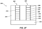
- a full liner 210 may be formed over the stacks 205 , as shown in FIG. 2E .
- portions of the materials overlying the substrate 220 may be removed to expose a top surface of the substrate 220 .
- portions of all the materials overlying the substrate 220 are removed until the top surface of the substrate 220 is exposed.
- the full liner 210 may be conformally formed over sidewalls and a top horizontal portion of the stacks 205 as well as the top surface of the substrate 220 in the trenches 215 .
- the material of the full liner 210 may be substantially the same as the material of the partial liner 225 .
- the full liner 210 may include alucone, alucone and aluminum oxide, a gradient of alucone, or combinations thereof.
- the full liner 210 may optionally include silicon atoms and/or nitride atoms as described above with reference to FIG. 1A through FIG. 1C .
- the full liner 210 may have a thickness as low as about 5 ⁇ or the full liner 210 may completely fill the trenches 215 . In some embodiments, the full liner 210 has a thickness ranging from between about 5 ⁇ and about 30 ⁇ . For example, the full liner 210 may have a thickness of between about 5 ⁇ and about 10 ⁇ , between about 10 ⁇ and about 20 ⁇ , or between about 20 ⁇ and about 30 ⁇ .
- the full liner 210 may be formed by conducting one or more ALD cycles, one or more MLD cycles, or combinations thereof. For example, the full liner 210 may be formed by performing one MLD cycle. In other embodiments, sufficient ALD and MLD cycles may be performed to completely fill the trenches 215 with the full liner 210 .
- the full liner 210 may be further processed to alter the chemistry of the full liner 210 after it has been deposited.
- the full liner 210 may be oxidized as previously described, to convert the alucone to aluminum oxide.
- the horizontal portions of the full liner 210 may be removed from a top horizontal portion of the stacks 205 and from a bottom horizontal portion of the trenches 215 so that sidewalls of the stacks 205 remain protected by the full liner 210 and a top surface of the stack 205 remains protected by the hard mask material 290 .
- a dry plasma etch as described above with respect to FIG. 2C may remove the full liner 210 from the tops of the stacks 205 and from bottom portions of the trenches 215 .
- the trenches 215 between adjacent stacks 205 may be filled with a dielectric material 235 such as a silicon dioxide material. Additional process acts may then be conducted to form a complete 3D cross-point memory structure 200 from the structure in FIG. 2F .
- the additional process acts may be formed by conventional techniques, which are not described in detail herein.
- the semiconductor device comprises stack structures comprising at least two chalcogenide materials overlying a substrate.
- a liner comprising alucone is on sidewalls of at least a portion of the stack structures.
- a method of forming a semiconductor device comprises forming stack structures over a substrate and forming a liner comprising alucone over the stack structures.
- the liner is removed from a bottom portion of trenches between the stack structures while leaving the liner on sidewalls of the stack structures.
- the alucone containing liner may be used in a 3D-NAND memory structure.
- a semiconductor structure 300 is shown that may be further processed to form a 3D-NAND flash memory device.
- the semiconductor structure 300 includes alternating conductive materials 350 and dielectric materials 340 formed over a substrate 320 .
- the alternating conductive materials 350 and dielectric materials 340 may be formed by conventional techniques.
- the substrate 320 may include a material similar to substrate 220 described with reference to FIG. 2A .
- the substrate 320 may include doped regions that form source and drain regions.
- a conductive material such as a source or drain may be formed on the substrate 320 or within the substrate 320 .
- a data/sense line (e.g., bit line, digit line, word line, etc.) (not shown), rather than a source or drain may be formed over the substrate 320 .
- the data/sense line may be formed from doped polysilicon, tungsten silicide, tungsten, or other conventional materials.
- a control gate material 330 may be formed over the substrate 320 .
- An etch stop material (not shown) may be formed over the control gate material 330 .
- the etch stop material may comprise an aluminum oxide material, a silicon nitride material, or other conventional material selected so that the materials of the stacks 305 may be selectively removed without removing the other materials of the semiconductor structure 300 .
- the control gate material 330 may comprise a control gate such as a select source gate (SSG) or a select gate drain (SGD) and may be electrically coupled to a source or drain region or a data/sense line on the substrate 320 .
- the control gate material 330 may comprise the same or different materials than the conductive material 350 .
- the dielectric material 340 may comprise an insulative material such as a silicon oxide.
- the alternating dielectric materials 340 comprise silicon dioxide.
- the conductive material 350 may comprise any known conductive material.
- the alternating conductive materials 350 may comprise n-doped polysilicon, p-doped polysilicon, undoped polysilicon, tungsten, aluminum, copper, titanium, tantalum, platinum, alloys thereof, conductive silicides, conductive nitrides, conductive carbides, or combinations thereof.
- the formation of the dielectric materials 340 and the conductive materials 350 may be repeated to form the alternating materials over the substrate 320 .
- a hard mask 390 may be formed over the 3D-NAND structure 300 .
- the hard mask 390 may be a nitride material such as a silicon nitride.
- a partial etch may form partial stacks 305 ′ by removing alternating portions of the conductive material 350 and the dielectric material 340 .
- the portions of the conductive material 350 and the dielectric material 340 may be removed with a single etch act, such as by reactive ion etching, dry plasma etching, an anisotropic dry etch process, or other suitable etching method.
- the partial etch may terminate on one of the dielectric materials 340 or on one of the conductive materials 350 .
- a partial liner 325 may be formed over the partial stacks 305 ′.
- the partial liner 325 may be conformally formed over the partial stacks 305 ′.
- the partial liner 325 may comprise materials as described above with reference to FIG. 1A through FIG. 1C , and may include alucone, alucone and aluminum oxide, a gradient of alucone, or combinations thereof.
- the partial liner 325 may optionally include silicon atoms and/or nitride atoms as described above with reference to FIG. 1A through FIG. 1C .
- an aluminum oxide portion of the partial liner 325 if present, may be in contact with the partial stacks 305 ′.
- the partial liner 325 may be removed from bottom portions of the trenches 315 .
- the partial liner 325 may be removed from a top horizontal surface of the partial stacks 305 ′.
- the partial liner 325 may be removed by a dry plasma etch.
- the plasma etch may be as described above with reference to FIG. 2C .
- a dry plasma etch may remove the partial liner 325 from the top horizontal surfaces of the partial stacks 305 ′ and the bottom portion of the trenches 315 without removing the partial liner 325 from sidewalls of the trenches 315 .
- these portions of the partial liner 325 may be removed without an aggressive wet etch chemistry that may damage the underlying partial stacks 305 ′.
- the partial liner 325 may be oxidized as previously described.
- the height of the partial stacks 305 ′ may be increased by continuing to remove exposed portions of the alternating dielectric materials 340 and conductive materials 350 , thereby forming stacks 305 .
- the depth of trenches 315 is increased.
- the alternating portions of the dielectric material 340 and the conductive material 350 may be removed as described above.
- the partial liner 325 may protect the alternating dielectric materials 340 and conductive materials 350 at upper portions of the stacks 305 from being damaged and the distance between adjacent stacks may not be increased during the etch.
- the etch may terminate at the etch stop material (not shown) over the control gate material 330 . In other embodiments, the etch may remove at least a portion of the control gate material 330 or at least a portion of the substrate 320 and may terminate on the control gate material 330 or on the substrate 320 .
- the full liner 310 or partial liner 325 is removed after the stacks 305 are formed. In other embodiments, the full liner 310 or partial liner 325 remains in the final structure. Referring to FIG. 3G , the full liner 310 may be removed from bottom portions of the trenches 315 . Although not shown, the full liner 310 may also be removed from a top horizontal surface of the stacks 305 .
- a charge trap comprising a tunnel dielectric, a charge trapping material, and a charge blocking material may be formed over the full liner 310 or partial liner 325 .
- the tunnel dielectric may comprise a silicon oxide such as silicon dioxide.
- a charge trapping material such as a silicon nitride may be formed over the tunnel dielectric.
- a charge blocking material such as a silicon oxide may be formed over the charge trapping material.
- an oxide-nitride-oxide (ONO) material may be formed over the material of the full liner 310 .
- the charge trap may comprise high-k dielectrics such as hafnium oxide, zirconium oxide, aluminum oxide, and low-k dielectrics, or combinations thereof may be formed over the material of the full liner 310 or partial liner 325 .
- the semiconductor device comprises stack structures comprising alternating dielectric materials and conductive materials overlying a substrate.
- a liner comprising alucone is on sidewalls of the stack structures.
Landscapes
- Engineering & Computer Science (AREA)
- Manufacturing & Machinery (AREA)
- Physics & Mathematics (AREA)
- Condensed Matter Physics & Semiconductors (AREA)
- General Physics & Mathematics (AREA)
- Computer Hardware Design (AREA)
- Microelectronics & Electronic Packaging (AREA)
- Power Engineering (AREA)
- Chemical & Material Sciences (AREA)
- Chemical Kinetics & Catalysis (AREA)
- Inorganic Chemistry (AREA)
- General Chemical & Material Sciences (AREA)
- Crystallography & Structural Chemistry (AREA)
- Semiconductor Memories (AREA)
Abstract
Description
-
- In some embodiments, a
full liner 310 may be formed over thestacks 305, as shown inFIG. 3F . Referring back toFIG. 3A , portions of the materials overlying thesubstrate 320 may be removed to expose a top surface of thesubstrate 320. Rather than terminating the etch on an intermediatedielectric material 340 or another intermediate material as inFIG. 3B , portions of all the alternatingdielectric materials 340 andconductive materials 350 overlying thesubstrate 320 are removed until the top surface of thesubstrate 320 is exposed, forming stacks 305. Thefull liner 310 may be conformally formed over thestacks 305. Thefull liner 310 may contact alternating portions of thedielectric material 340 and theconductive material 350, thecontrol gate material 330, and a portion of thesubstrate 320. Thefull liner 310 may be formed as described above with reference toFIG. 1A throughFIG. 1C and may include alucone, alucone and aluminum oxide, a gradient of alucone, or combinations thereof. In some embodiments, thefull liner 210 may optionally include silicon atoms and/or nitride atoms as described above with reference toFIG. 1A throughFIG. 1C . In some embodiments, thefull liner 310 is oxidized as previously described.
- In some embodiments, a
Claims (18)
Priority Applications (1)
| Application Number | Priority Date | Filing Date | Title |
|---|---|---|---|
| US16/446,746 US11223014B2 (en) | 2014-02-25 | 2019-06-20 | Semiconductor structures including liners comprising alucone and related methods |
Applications Claiming Priority (3)
| Application Number | Priority Date | Filing Date | Title |
|---|---|---|---|
| US14/189,323 US9484196B2 (en) | 2014-02-25 | 2014-02-25 | Semiconductor structures including liners comprising alucone and related methods |
| US15/244,629 US10573513B2 (en) | 2014-02-25 | 2016-08-23 | Semiconductor structures including liners comprising alucone and related methods |
| US16/446,746 US11223014B2 (en) | 2014-02-25 | 2019-06-20 | Semiconductor structures including liners comprising alucone and related methods |
Related Parent Applications (1)
| Application Number | Title | Priority Date | Filing Date |
|---|---|---|---|
| US15/244,629 Continuation US10573513B2 (en) | 2014-02-25 | 2016-08-23 | Semiconductor structures including liners comprising alucone and related methods |
Publications (2)
| Publication Number | Publication Date |
|---|---|
| US20190312200A1 US20190312200A1 (en) | 2019-10-10 |
| US11223014B2 true US11223014B2 (en) | 2022-01-11 |
Family
ID=68097393
Family Applications (1)
| Application Number | Title | Priority Date | Filing Date |
|---|---|---|---|
| US16/446,746 Active 2034-09-16 US11223014B2 (en) | 2014-02-25 | 2019-06-20 | Semiconductor structures including liners comprising alucone and related methods |
Country Status (1)
| Country | Link |
|---|---|
| US (1) | US11223014B2 (en) |
Cited By (1)
| Publication number | Priority date | Publication date | Assignee | Title |
|---|---|---|---|---|
| US12091251B2 (en) | 2019-09-19 | 2024-09-17 | Beijing Jingdong Qianshi Technology Co., Ltd. | Storage system |
Families Citing this family (1)
| Publication number | Priority date | Publication date | Assignee | Title |
|---|---|---|---|---|
| US20220359332A1 (en) * | 2021-05-09 | 2022-11-10 | Spts Technologies Limited | Temporary passivation layer on a substrate |
Citations (81)
| Publication number | Priority date | Publication date | Assignee | Title |
|---|---|---|---|---|
| US6404003B1 (en) | 1999-07-28 | 2002-06-11 | Symetrix Corporation | Thin film capacitors on silicon germanium substrate |
| US6486070B1 (en) | 2000-09-21 | 2002-11-26 | Lam Research Corporation | Ultra-high oxide to photoresist selective etch of high-aspect-ratio openings in a low-pressure, high-density plasma |
| US20030142944A1 (en) | 2001-09-17 | 2003-07-31 | Sundar Vikram C. | Semiconductor nanocrystal composite |
| KR20040068024A (en) | 2003-01-23 | 2004-07-30 | 샤프 가부시키가이샤 | Dual-trench isolated crosspoint memory array and method for fabricating same |
| US20040227227A1 (en) | 2003-05-15 | 2004-11-18 | Fujitsu Limited | Aerosol deposition process |
| US20050167842A1 (en) | 2004-01-15 | 2005-08-04 | Naofumi Nakamura | Semiconductor device |
| US20050263829A1 (en) | 2004-05-27 | 2005-12-01 | Yoon-Jong Song | Semiconductor devices having phase change memory cells, electronic systems employing the same and methods of fabricating the same |
| US20060056233A1 (en) | 2004-09-10 | 2006-03-16 | Parkinson Ward D | Using a phase change memory as a replacement for a buffered flash memory |
| US20060097240A1 (en) | 2004-11-08 | 2006-05-11 | Tyler Lowrey | Programmable matrix array with chalcogenide material |
| US7215564B2 (en) | 2004-04-27 | 2007-05-08 | Infineon Technologies Ag | Semiconductor memory component in cross-point architecture |
| US20070105306A1 (en) | 2005-11-04 | 2007-05-10 | Freescale Semiconductor, Inc. | Nanocrystal bitcell process integration for high density application |
| US20070117256A1 (en) | 2005-11-23 | 2007-05-24 | Duncan Stewart | Control layer for a nanoscale electronic switching device |
| US20070166980A1 (en) | 2004-12-30 | 2007-07-19 | Stmicroelectronics S.R.I. | Chemical vapor deposition chamber for depositing titanium silicon nitride films for forming phase change memory devices |
| US20070275560A1 (en) | 2006-02-22 | 2007-11-29 | Eiichi Nishimura | Method of manufacturing semiconductor device |
| US20080102560A1 (en) | 2006-10-10 | 2008-05-01 | Stmicroelectronics S.R.L. | Method of forming phase change memory devices in a pulsed DC deposition chamber |
| US20080124917A1 (en) | 2006-11-23 | 2008-05-29 | Samsung Electronics Co., Ltd. | Method of manufacturing a semiconductor device having air gaps |
| KR20080060321A (en) | 2006-12-27 | 2008-07-02 | 주식회사 하이닉스반도체 | Method for etching semiconductor device with multi layer stack |
| US20080293207A1 (en) | 2007-05-25 | 2008-11-27 | Koutny Jr William W C | Integration of non-volatile charge trap memory devices and logic cmos devices |
| US20080315359A1 (en) | 2007-06-21 | 2008-12-25 | Thomas Happ | Integrated circuit including vertical diode |
| US20090072274A1 (en) | 2007-09-14 | 2009-03-19 | Qimonda Ag | Integrated circuit including a first gate stack and a second gate stack and a method of manufacturing |
| US20090231911A1 (en) | 2008-03-14 | 2009-09-17 | Micron Technology, Inc. | Phase change memory cell with constriction structure |
| US20090251944A1 (en) | 2008-04-07 | 2009-10-08 | Macronix International Co., Ltd. | Memory cell having improved mechanical stability |
| US20090302362A1 (en) | 2007-03-14 | 2009-12-10 | Fujitsu Microelectronics Limited | Semiconductor device and method of manufacturing the same |
| US20100032637A1 (en) | 2008-08-06 | 2010-02-11 | Hitachi, Ltd. | Nonvolatile memory device and method of manufacturing the same |
| US7700472B2 (en) | 2006-12-28 | 2010-04-20 | Hynix Semiconductor Inc. | Method of forming a gate of a semiconductor device |
| US20100155723A1 (en) * | 2008-12-19 | 2010-06-24 | Unity Semiconductor Corporation | Memory stack cladding |
| US20100163818A1 (en) | 2008-12-30 | 2010-07-01 | Stmicroelectronics S.R.L. | Forming a carbon passivated ovonic threshold switch |
| US20100237502A1 (en) | 2009-03-23 | 2010-09-23 | Taiwan Semiconductor Manufacturing Company, Ltd. | Barrier for Through-Silicon Via |
| US20110068313A1 (en) | 2009-09-21 | 2011-03-24 | Micron Technology, Inc. | Memory devices with enhanced isolation of memory cells, systems including same and methods of forming same |
| US7936027B2 (en) | 2008-01-07 | 2011-05-03 | Magic Technologies, Inc. | Method of MRAM fabrication with zero electrical shorting |
| US20110244666A1 (en) | 2010-04-05 | 2011-10-06 | Samsung Electronics Co., Ltd. | Methods Of Manufacturing Stair-Type Structures And Methods Of Manufacturing Nonvolatile Memory Devices Using The Same |
| US20110272664A1 (en) | 2009-01-09 | 2011-11-10 | Munehiro Tada | Semiconductor device and method of manufacturing the same |
| US20120001145A1 (en) | 2008-12-31 | 2012-01-05 | Michele Magistretti | Avoiding degradation of chalcogenide material during definition of multilayer stack structure |
| US20120040528A1 (en) | 2010-08-13 | 2012-02-16 | Samsung Electronics Co., Ltd. | Methods for patterning microelectronic devices using two sacrificial layers |
| US8143610B2 (en) | 2009-01-05 | 2012-03-27 | Samsung Electronics Co., Ltd. | Semiconductor phase-change memory device |
| US20120080792A1 (en) | 2010-09-30 | 2012-04-05 | Institute of Microelectronics, Chinese Academy of Sciences | Metal Interconnection Structure and Method For Forming Metal Interlayer Via and Metal Interconnection Line |
| US8153527B2 (en) | 2008-10-13 | 2012-04-10 | Globalfoundries Singapore Pte. Ltd. | Method for reducing sidewall etch residue |
| US20120098146A1 (en) | 2010-10-21 | 2012-04-26 | Synos Technology, Inc. | Formation of barrier layer on device using atomic layer deposition |
| US8207557B2 (en) | 2009-02-19 | 2012-06-26 | Micron Technology, Inc. | Cross-point memory structures |
| US20120181596A1 (en) | 2011-01-14 | 2012-07-19 | Micron Technology, Inc. | Strings of memory cells having string select gates, memory devices incorporating such strings, and methods of accessing and forming the same |
| US8237213B2 (en) | 2010-07-15 | 2012-08-07 | Micron Technology, Inc. | Memory arrays having substantially vertical, adjacent semiconductor structures and the formation thereof |
| US20120220099A1 (en) | 2005-10-28 | 2012-08-30 | Dennison Charles H | Forming a Phase Change Memory With an Ovonic Threshold Switch |
| US20120225534A1 (en) | 2009-11-30 | 2012-09-06 | Micron Technology, Inc. | Self-aligned cross-point phase change memory-switch array |
| US20120236642A1 (en) | 2009-03-03 | 2012-09-20 | Macronix International Co., Ltd. | Integrated circuit self aligned 3d memory array and manufacturing method |
| US20120235109A1 (en) | 2011-03-18 | 2012-09-20 | Kabushiki Kaisha Toshiba | Non-volatile semiconductor storage device and manufacturing method of non-volatile semiconductor storage device |
| US20120313064A1 (en) | 2011-06-10 | 2012-12-13 | Kabushiki Kaisha Toshiba | Semiconductor memory device and method for manufacturing the same |
| US20120313199A1 (en) | 2011-05-26 | 2012-12-13 | Hitachi Chemical Company, Ltd. | Material for forming passivation film for semiconductor substrate, passivation film for semiconductor substrate and method of producing the same, and photovoltaic cell element and method of producing the same |
| US20120315384A1 (en) | 2011-06-07 | 2012-12-13 | GM Global Technology Operations LLC | Method of applying nonconductive ceramics on lithium-ion battery separators |
| US20130016557A1 (en) | 2010-04-05 | 2013-01-17 | Mosaid Technologies Incorporated | Semiconductor memory device having a three-dimensional structure |
| US20130043455A1 (en) | 2011-08-15 | 2013-02-21 | Unity Semiconductor Corporation | Vertical Cross Point Arrays For Ultra High Density Memory Applications |
| US20130056698A1 (en) | 2011-09-03 | 2013-03-07 | Kimihiro Satoh | Resistive memory device having vertical transistors and method for making the same |
| US8394683B2 (en) | 2008-01-15 | 2013-03-12 | Micron Technology, Inc. | Methods of forming semiconductor constructions, and methods of forming NAND unit cells |
| US8450714B2 (en) | 2010-03-19 | 2013-05-28 | Kabushiki Kaisha Toshiba | Semiconductor memory device including variable resistance element or phase-change element |
| US20130137275A1 (en) | 2011-11-29 | 2013-05-30 | Intermolecular, Inc. | Methods for selective etching of a multi-layer substrate |
| US20130207068A1 (en) | 2012-02-09 | 2013-08-15 | Micron Technology, Inc. | Memory cells and memory cell formation methods using sealing material |
| US8519371B2 (en) | 2008-03-07 | 2013-08-27 | Kabushiki Kaisha Toshiba | Nonvolatile memory device and method for manufacturing the same |
| US8536015B2 (en) | 2008-04-11 | 2013-09-17 | Sandisk 3D Llc | Memory cell that includes a carbon-based memory element and methods of forming the same |
| US20130294152A1 (en) | 2012-05-07 | 2013-11-07 | DerChang Kau | Apparatuses and methods including memory access in cross point memory |
| US20130333835A1 (en) | 2012-06-14 | 2013-12-19 | E I Du Pont De Nemours And Company | Process for manufacturing gas permeation barrier material and structure |
| US20140048795A1 (en) | 2012-08-14 | 2014-02-20 | Industry Academy Cooperation Foundation Of Kyunghee University | Thin film transistor and method of manufacturing the same and display device including the same |
| US20140170234A1 (en) | 2010-08-19 | 2014-06-19 | Allergan, Inc. | Compositions and improved soft tissue replacement methods |
| US20140168490A1 (en) | 2011-04-22 | 2014-06-19 | Panasonic Corporation | Imaging device, imaging system, and imaging method |
| US20140190565A1 (en) | 2013-01-09 | 2014-07-10 | Research & Business Foundation Sungkyunkwan University | Polymer/inorganic multi-layer encapsulation film |
| US8822968B2 (en) | 2012-03-26 | 2014-09-02 | Kabushiki Kaisha Toshiba | Nonvolatile memory device and method for manufacturing same |
| US20140273524A1 (en) | 2013-03-12 | 2014-09-18 | Victor Nguyen | Plasma Doping Of Silicon-Containing Films |
| US20140273516A1 (en) | 2013-03-13 | 2014-09-18 | Applied Materials, Inc. | Vbd and tddb improvement thru interface engineering |
| US8902634B2 (en) | 2012-09-12 | 2014-12-02 | Kabushiki Kaisha Toshiba | Resistance change type memory and manufacturing method thereof |
| US20150041749A1 (en) | 2013-08-06 | 2015-02-12 | Micron Technology, Inc. | Memory Cells and Methods of Forming Memory Cells |
| US20150069581A1 (en) | 2013-09-11 | 2015-03-12 | Taiwan Semiconductor Manufacturing Co., Ltd. | Noble gas bombardment to reduce scallops in bosch etching |
| US20150069559A1 (en) | 2013-09-09 | 2015-03-12 | Shuichi TSUBATA | Nonvolatile semiconductor memory device and method of manufacturing the same |
| US20150069473A1 (en) | 2013-09-06 | 2015-03-12 | Glenn A. Glass | Transistor fabrication technique including sacrificial protective layer for source/drain at contact location |
| US20150137061A1 (en) | 2013-11-21 | 2015-05-21 | Micron Technology, Inc. | Cross-point memory and methods for fabrication of same |
| US20150171324A1 (en) | 2012-01-19 | 2015-06-18 | Panasonic Corporation | Method of manufacturing variable resistance nonvolatile memory device, and variable resistance nonvolatile memory device |
| WO2015088921A1 (en) | 2013-12-13 | 2015-06-18 | Micron Technology, Inc. | Methods of forming metal on inhomogeneous surfaces and structures incorporating metal on inhomogeneous surfaces |
| US20150179706A1 (en) | 2013-12-20 | 2015-06-25 | Noel Rocklein | Liner for phase change memory (pcm) array and associated techniques and configurations |
| US20150243709A1 (en) | 2014-02-25 | 2015-08-27 | Micron Technology, Inc. | Semiconductor structures including liners comprising alucone and related methods |
| US20150243708A1 (en) | 2014-02-25 | 2015-08-27 | Micron Technology, Inc. | Cross-point memory and methods for fabrication of same |
| US20150243885A1 (en) | 2014-02-25 | 2015-08-27 | Micron Technology, Inc. | Cross-point memory and methods for fabrication of same |
| US20150287916A1 (en) | 2014-04-03 | 2015-10-08 | Micron Technology, Inc. | Semiconductor structures including multi-portion liners and related methods |
| US20160056208A1 (en) | 2014-08-25 | 2016-02-25 | Micron Technology, Inc. | Cross-point memory and methods for fabrication of same |
| US20160133671A1 (en) | 2014-11-07 | 2016-05-12 | Micron Technology, Inc. | Cross-point memory and methods for fabrication of same |
-
2019
- 2019-06-20 US US16/446,746 patent/US11223014B2/en active Active
Patent Citations (100)
| Publication number | Priority date | Publication date | Assignee | Title |
|---|---|---|---|---|
| US6404003B1 (en) | 1999-07-28 | 2002-06-11 | Symetrix Corporation | Thin film capacitors on silicon germanium substrate |
| US6486070B1 (en) | 2000-09-21 | 2002-11-26 | Lam Research Corporation | Ultra-high oxide to photoresist selective etch of high-aspect-ratio openings in a low-pressure, high-density plasma |
| US20030142944A1 (en) | 2001-09-17 | 2003-07-31 | Sundar Vikram C. | Semiconductor nanocrystal composite |
| KR20040068024A (en) | 2003-01-23 | 2004-07-30 | 샤프 가부시키가이샤 | Dual-trench isolated crosspoint memory array and method for fabricating same |
| US20040227227A1 (en) | 2003-05-15 | 2004-11-18 | Fujitsu Limited | Aerosol deposition process |
| US20050167842A1 (en) | 2004-01-15 | 2005-08-04 | Naofumi Nakamura | Semiconductor device |
| US7215564B2 (en) | 2004-04-27 | 2007-05-08 | Infineon Technologies Ag | Semiconductor memory component in cross-point architecture |
| US7482616B2 (en) | 2004-05-27 | 2009-01-27 | Samsung Electronics Co., Ltd. | Semiconductor devices having phase change memory cells, electronic systems employing the same and methods of fabricating the same |
| US20050263829A1 (en) | 2004-05-27 | 2005-12-01 | Yoon-Jong Song | Semiconductor devices having phase change memory cells, electronic systems employing the same and methods of fabricating the same |
| US20060056233A1 (en) | 2004-09-10 | 2006-03-16 | Parkinson Ward D | Using a phase change memory as a replacement for a buffered flash memory |
| US20060097240A1 (en) | 2004-11-08 | 2006-05-11 | Tyler Lowrey | Programmable matrix array with chalcogenide material |
| US20070166980A1 (en) | 2004-12-30 | 2007-07-19 | Stmicroelectronics S.R.I. | Chemical vapor deposition chamber for depositing titanium silicon nitride films for forming phase change memory devices |
| US20120220099A1 (en) | 2005-10-28 | 2012-08-30 | Dennison Charles H | Forming a Phase Change Memory With an Ovonic Threshold Switch |
| US20070105306A1 (en) | 2005-11-04 | 2007-05-10 | Freescale Semiconductor, Inc. | Nanocrystal bitcell process integration for high density application |
| US7491600B2 (en) | 2005-11-04 | 2009-02-17 | Freescale Semiconductor, Inc. | Nanocrystal bitcell process integration for high density application |
| US20070117256A1 (en) | 2005-11-23 | 2007-05-24 | Duncan Stewart | Control layer for a nanoscale electronic switching device |
| US7741638B2 (en) | 2005-11-23 | 2010-06-22 | Hewlett-Packard Development Company, L.P. | Control layer for a nanoscale electronic switching device |
| US20070275560A1 (en) | 2006-02-22 | 2007-11-29 | Eiichi Nishimura | Method of manufacturing semiconductor device |
| US20080102560A1 (en) | 2006-10-10 | 2008-05-01 | Stmicroelectronics S.R.L. | Method of forming phase change memory devices in a pulsed DC deposition chamber |
| US20080124917A1 (en) | 2006-11-23 | 2008-05-29 | Samsung Electronics Co., Ltd. | Method of manufacturing a semiconductor device having air gaps |
| KR20080060321A (en) | 2006-12-27 | 2008-07-02 | 주식회사 하이닉스반도체 | Method for etching semiconductor device with multi layer stack |
| US7700472B2 (en) | 2006-12-28 | 2010-04-20 | Hynix Semiconductor Inc. | Method of forming a gate of a semiconductor device |
| US20090302362A1 (en) | 2007-03-14 | 2009-12-10 | Fujitsu Microelectronics Limited | Semiconductor device and method of manufacturing the same |
| US20080293207A1 (en) | 2007-05-25 | 2008-11-27 | Koutny Jr William W C | Integration of non-volatile charge trap memory devices and logic cmos devices |
| US20080315359A1 (en) | 2007-06-21 | 2008-12-25 | Thomas Happ | Integrated circuit including vertical diode |
| US7838860B2 (en) | 2007-06-21 | 2010-11-23 | Qimonda Ag | Integrated circuit including vertical diode |
| US7875516B2 (en) | 2007-09-14 | 2011-01-25 | Qimonda Ag | Integrated circuit including a first gate stack and a second gate stack and a method of manufacturing |
| US20090072274A1 (en) | 2007-09-14 | 2009-03-19 | Qimonda Ag | Integrated circuit including a first gate stack and a second gate stack and a method of manufacturing |
| US7936027B2 (en) | 2008-01-07 | 2011-05-03 | Magic Technologies, Inc. | Method of MRAM fabrication with zero electrical shorting |
| US8394683B2 (en) | 2008-01-15 | 2013-03-12 | Micron Technology, Inc. | Methods of forming semiconductor constructions, and methods of forming NAND unit cells |
| US8519371B2 (en) | 2008-03-07 | 2013-08-27 | Kabushiki Kaisha Toshiba | Nonvolatile memory device and method for manufacturing the same |
| US20090231911A1 (en) | 2008-03-14 | 2009-09-17 | Micron Technology, Inc. | Phase change memory cell with constriction structure |
| US20090251944A1 (en) | 2008-04-07 | 2009-10-08 | Macronix International Co., Ltd. | Memory cell having improved mechanical stability |
| US8536015B2 (en) | 2008-04-11 | 2013-09-17 | Sandisk 3D Llc | Memory cell that includes a carbon-based memory element and methods of forming the same |
| KR20100018445A (en) | 2008-08-06 | 2010-02-17 | 가부시키가이샤 히타치세이사쿠쇼 | Nonvolatile memory device and manufacturing method thereof |
| US8129705B2 (en) | 2008-08-06 | 2012-03-06 | Hitachi, Ltd. | Nonvolatile memory device and method of manufacturing the same |
| US20100032637A1 (en) | 2008-08-06 | 2010-02-11 | Hitachi, Ltd. | Nonvolatile memory device and method of manufacturing the same |
| US8153527B2 (en) | 2008-10-13 | 2012-04-10 | Globalfoundries Singapore Pte. Ltd. | Method for reducing sidewall etch residue |
| US20100155723A1 (en) * | 2008-12-19 | 2010-06-24 | Unity Semiconductor Corporation | Memory stack cladding |
| US20100163818A1 (en) | 2008-12-30 | 2010-07-01 | Stmicroelectronics S.R.L. | Forming a carbon passivated ovonic threshold switch |
| US20120001145A1 (en) | 2008-12-31 | 2012-01-05 | Michele Magistretti | Avoiding degradation of chalcogenide material during definition of multilayer stack structure |
| US8143610B2 (en) | 2009-01-05 | 2012-03-27 | Samsung Electronics Co., Ltd. | Semiconductor phase-change memory device |
| US20110272664A1 (en) | 2009-01-09 | 2011-11-10 | Munehiro Tada | Semiconductor device and method of manufacturing the same |
| US9406877B2 (en) | 2009-01-09 | 2016-08-02 | Nec Corporation | Semiconductor device and method of manufacturing the same |
| US8207557B2 (en) | 2009-02-19 | 2012-06-26 | Micron Technology, Inc. | Cross-point memory structures |
| US20120236642A1 (en) | 2009-03-03 | 2012-09-20 | Macronix International Co., Ltd. | Integrated circuit self aligned 3d memory array and manufacturing method |
| US20100237502A1 (en) | 2009-03-23 | 2010-09-23 | Taiwan Semiconductor Manufacturing Company, Ltd. | Barrier for Through-Silicon Via |
| US20110068313A1 (en) | 2009-09-21 | 2011-03-24 | Micron Technology, Inc. | Memory devices with enhanced isolation of memory cells, systems including same and methods of forming same |
| US8203134B2 (en) | 2009-09-21 | 2012-06-19 | Micron Technology, Inc. | Memory devices with enhanced isolation of memory cells, systems including same and methods of forming same |
| US20120225534A1 (en) | 2009-11-30 | 2012-09-06 | Micron Technology, Inc. | Self-aligned cross-point phase change memory-switch array |
| US8450714B2 (en) | 2010-03-19 | 2013-05-28 | Kabushiki Kaisha Toshiba | Semiconductor memory device including variable resistance element or phase-change element |
| US20130016557A1 (en) | 2010-04-05 | 2013-01-17 | Mosaid Technologies Incorporated | Semiconductor memory device having a three-dimensional structure |
| US20110244666A1 (en) | 2010-04-05 | 2011-10-06 | Samsung Electronics Co., Ltd. | Methods Of Manufacturing Stair-Type Structures And Methods Of Manufacturing Nonvolatile Memory Devices Using The Same |
| US8237213B2 (en) | 2010-07-15 | 2012-08-07 | Micron Technology, Inc. | Memory arrays having substantially vertical, adjacent semiconductor structures and the formation thereof |
| US9012326B2 (en) | 2010-08-13 | 2015-04-21 | Samsung Electronics Co., Ltd. | Methods for patterning microelectronic devices using two sacrificial layers |
| US20120040528A1 (en) | 2010-08-13 | 2012-02-16 | Samsung Electronics Co., Ltd. | Methods for patterning microelectronic devices using two sacrificial layers |
| US20140170234A1 (en) | 2010-08-19 | 2014-06-19 | Allergan, Inc. | Compositions and improved soft tissue replacement methods |
| US20120080792A1 (en) | 2010-09-30 | 2012-04-05 | Institute of Microelectronics, Chinese Academy of Sciences | Metal Interconnection Structure and Method For Forming Metal Interlayer Via and Metal Interconnection Line |
| US20120098146A1 (en) | 2010-10-21 | 2012-04-26 | Synos Technology, Inc. | Formation of barrier layer on device using atomic layer deposition |
| US20120181596A1 (en) | 2011-01-14 | 2012-07-19 | Micron Technology, Inc. | Strings of memory cells having string select gates, memory devices incorporating such strings, and methods of accessing and forming the same |
| US20120235109A1 (en) | 2011-03-18 | 2012-09-20 | Kabushiki Kaisha Toshiba | Non-volatile semiconductor storage device and manufacturing method of non-volatile semiconductor storage device |
| US20140168490A1 (en) | 2011-04-22 | 2014-06-19 | Panasonic Corporation | Imaging device, imaging system, and imaging method |
| US20120313199A1 (en) | 2011-05-26 | 2012-12-13 | Hitachi Chemical Company, Ltd. | Material for forming passivation film for semiconductor substrate, passivation film for semiconductor substrate and method of producing the same, and photovoltaic cell element and method of producing the same |
| US20120315384A1 (en) | 2011-06-07 | 2012-12-13 | GM Global Technology Operations LLC | Method of applying nonconductive ceramics on lithium-ion battery separators |
| US20120313064A1 (en) | 2011-06-10 | 2012-12-13 | Kabushiki Kaisha Toshiba | Semiconductor memory device and method for manufacturing the same |
| US20130043455A1 (en) | 2011-08-15 | 2013-02-21 | Unity Semiconductor Corporation | Vertical Cross Point Arrays For Ultra High Density Memory Applications |
| US8937292B2 (en) | 2011-08-15 | 2015-01-20 | Unity Semiconductor Corporation | Vertical cross point arrays for ultra high density memory applications |
| US20130056698A1 (en) | 2011-09-03 | 2013-03-07 | Kimihiro Satoh | Resistive memory device having vertical transistors and method for making the same |
| US20130137275A1 (en) | 2011-11-29 | 2013-05-30 | Intermolecular, Inc. | Methods for selective etching of a multi-layer substrate |
| US20150171324A1 (en) | 2012-01-19 | 2015-06-18 | Panasonic Corporation | Method of manufacturing variable resistance nonvolatile memory device, and variable resistance nonvolatile memory device |
| US20130207068A1 (en) | 2012-02-09 | 2013-08-15 | Micron Technology, Inc. | Memory cells and memory cell formation methods using sealing material |
| US9136307B2 (en) | 2012-02-09 | 2015-09-15 | Micron Technology, Inc. | Memory cells and memory cell formation methods using sealing material |
| US8822968B2 (en) | 2012-03-26 | 2014-09-02 | Kabushiki Kaisha Toshiba | Nonvolatile memory device and method for manufacturing same |
| US20130294152A1 (en) | 2012-05-07 | 2013-11-07 | DerChang Kau | Apparatuses and methods including memory access in cross point memory |
| US20130333835A1 (en) | 2012-06-14 | 2013-12-19 | E I Du Pont De Nemours And Company | Process for manufacturing gas permeation barrier material and structure |
| US20140048795A1 (en) | 2012-08-14 | 2014-02-20 | Industry Academy Cooperation Foundation Of Kyunghee University | Thin film transistor and method of manufacturing the same and display device including the same |
| US8902634B2 (en) | 2012-09-12 | 2014-12-02 | Kabushiki Kaisha Toshiba | Resistance change type memory and manufacturing method thereof |
| US20140190565A1 (en) | 2013-01-09 | 2014-07-10 | Research & Business Foundation Sungkyunkwan University | Polymer/inorganic multi-layer encapsulation film |
| US20140273524A1 (en) | 2013-03-12 | 2014-09-18 | Victor Nguyen | Plasma Doping Of Silicon-Containing Films |
| US20140273516A1 (en) | 2013-03-13 | 2014-09-18 | Applied Materials, Inc. | Vbd and tddb improvement thru interface engineering |
| US20150041749A1 (en) | 2013-08-06 | 2015-02-12 | Micron Technology, Inc. | Memory Cells and Methods of Forming Memory Cells |
| US20150069473A1 (en) | 2013-09-06 | 2015-03-12 | Glenn A. Glass | Transistor fabrication technique including sacrificial protective layer for source/drain at contact location |
| US9093632B2 (en) | 2013-09-09 | 2015-07-28 | Shuichi TSUBATA | Nonvolatile semiconductor memory device and method of manufacturing the same |
| US20150069559A1 (en) | 2013-09-09 | 2015-03-12 | Shuichi TSUBATA | Nonvolatile semiconductor memory device and method of manufacturing the same |
| US20150069581A1 (en) | 2013-09-11 | 2015-03-12 | Taiwan Semiconductor Manufacturing Co., Ltd. | Noble gas bombardment to reduce scallops in bosch etching |
| US9224615B2 (en) | 2013-09-11 | 2015-12-29 | Taiwan Semiconductor Manufacturing Co., Ltd. | Noble gas bombardment to reduce scallops in bosch etching |
| US20150137061A1 (en) | 2013-11-21 | 2015-05-21 | Micron Technology, Inc. | Cross-point memory and methods for fabrication of same |
| WO2015088921A1 (en) | 2013-12-13 | 2015-06-18 | Micron Technology, Inc. | Methods of forming metal on inhomogeneous surfaces and structures incorporating metal on inhomogeneous surfaces |
| US20150179706A1 (en) | 2013-12-20 | 2015-06-25 | Noel Rocklein | Liner for phase change memory (pcm) array and associated techniques and configurations |
| US20150243885A1 (en) | 2014-02-25 | 2015-08-27 | Micron Technology, Inc. | Cross-point memory and methods for fabrication of same |
| US20150243708A1 (en) | 2014-02-25 | 2015-08-27 | Micron Technology, Inc. | Cross-point memory and methods for fabrication of same |
| US10573513B2 (en) * | 2014-02-25 | 2020-02-25 | Micron Technology, Inc. | Semiconductor structures including liners comprising alucone and related methods |
| US20150243709A1 (en) | 2014-02-25 | 2015-08-27 | Micron Technology, Inc. | Semiconductor structures including liners comprising alucone and related methods |
| US9484196B2 (en) * | 2014-02-25 | 2016-11-01 | Micron Technology, Inc. | Semiconductor structures including liners comprising alucone and related methods |
| US10249819B2 (en) | 2014-04-03 | 2019-04-02 | Micron Technology, Inc. | Methods of forming semiconductor structures including multi-portion liners |
| US10665782B2 (en) | 2014-04-03 | 2020-05-26 | Micron Technology, Inc. | Methods of forming semiconductor structures including multi-portion liners |
| US20150287916A1 (en) | 2014-04-03 | 2015-10-08 | Micron Technology, Inc. | Semiconductor structures including multi-portion liners and related methods |
| US20160056208A1 (en) | 2014-08-25 | 2016-02-25 | Micron Technology, Inc. | Cross-point memory and methods for fabrication of same |
| US20160133671A1 (en) | 2014-11-07 | 2016-05-12 | Micron Technology, Inc. | Cross-point memory and methods for fabrication of same |
| US9748311B2 (en) | 2014-11-07 | 2017-08-29 | Micron Technology, Inc. | Cross-point memory and methods for fabrication of same |
Non-Patent Citations (14)
| Title |
|---|
| "Current Status of the Phase Change Memory and its Future", 2003 IEEE. |
| "Fabrication of the Si2Sb2Te5 Phase Change Cell Structure for PCRAM by Using UV Nanoimprint Lithography", 2008 IEEE. |
| Dameron et al., Molecular Layer Deposition of Alucone Polymer Films Using Trimethylaluminum and Ethylene Glycol, Chem. Mater, vol. 20, (2008), pp. 3315-3326. |
| Gonzalez et al., Charge Trapping Analysis of Al2O3 Films Deposited by Atomic Layer Deposition Using H2O or O3 as Oxidant, J. Vacuum Sci. & Tech., vol. B 31, 01A101, 6 pages. |
| Jen et al., Critical Tensile Strain and Water Vapor Transmission Rate for Nanolaminate Films Grown Using Al2O3 Atomic Layer Deposition and Alucone Molecular Layer Deposition, Applied Physics Letters, vol. 101, (2012), pp. 234103-1-234103-3. |
| Lee et al. Alucone Alloys with Tunable Properties Using Alucone Molecular Layer Deposition and Al2O3 Atomic Layer Deposition, J. Phys. Chem. C, 116 (2012) pp. 3250-3257. |
| Lee et al., Characteristics of SiOC(-H) Thin Films Prepared by Using Plasma-Enhanced Atomic Layer Deposition, Journal of the Korean Physical Society, vol. 59, No. 5, Nov. 2011, pp. 3074-3079. |
| Lee et al., Growth and Properties of Hybrid Organic-Inorganic Melalcone Films Using Molecular Layer Deposition Techniques, Adv. Funct. Mater., vol. 23, (2013), pp. 532-546. |
| Miller et al., Termomechanical Properties of Aluminum Alkoxide (Alucone) Films Created Using Molecular Layer Deposition, Acta Malerialia, vol. 57 (2009), pp. 5083-5092. |
| Miller et al., Thermo-Mechanical Poperties of Alumina Films Created Using the Atomic Layer Deposition Technique, Sensorsand Actuators A: Physical, vol. 164 (2010), pp. 58-67. |
| Park et al. Gas diffusion barrier characteristics of Al2O3/alucone films formed using trimethylaluminum, water and ethylene glycol for organic light emitting diode encapsulation, Thin Solid Films, 546, 2013, pp. 153-156. (Year: 2013). * |
| Seghete et al., Sacrificial Layers for Air Gaps in NEMS Using Alucone Molecular Layer Deposition, Sensors and Actuators A:Physical, (2009), doi: 10.1016/j.sna.2008.12.016, 8 pages. |
| Sniegowski et al. IC-Compatible Polysilicon Surface Micromachining, Annu. Rev. Mater. Sci. 30 (2000) pp. 299-333. |
| Yoon et al. Molecular Layer Deposition of Hybrid Organic-Inorganic Alucone Polymer Films Using a Three-Step ABC Reaction Sequence, Chem. Mater. 21 (2009) pp. 5365-5374. |
Cited By (1)
| Publication number | Priority date | Publication date | Assignee | Title |
|---|---|---|---|---|
| US12091251B2 (en) | 2019-09-19 | 2024-09-17 | Beijing Jingdong Qianshi Technology Co., Ltd. | Storage system |
Also Published As
| Publication number | Publication date |
|---|---|
| US20190312200A1 (en) | 2019-10-10 |
Similar Documents
| Publication | Publication Date | Title |
|---|---|---|
| US10573513B2 (en) | Semiconductor structures including liners comprising alucone and related methods | |
| US10879462B2 (en) | Devices including multi-portion liners | |
| US11387347B2 (en) | Fin structures having varied fin heights for semiconductor device | |
| US11024627B2 (en) | High-K metal gate transistor structure and fabrication method thereof | |
| CN102737974B (en) | Method of fabricating a plurality of gate structures | |
| US12014960B2 (en) | Etch profile control of polysilicon structures of semiconductor devices | |
| US7838356B2 (en) | Gate dielectric first replacement gate processes and integrated circuits therefrom | |
| US11569125B2 (en) | Etch profile control of interconnect structures | |
| US12027424B2 (en) | Semiconductor integrated circuit | |
| US11145749B2 (en) | Method of fabricating a semiconductor device | |
| KR20080060376A (en) | Method for manufacturing semiconductor device | |
| US11223014B2 (en) | Semiconductor structures including liners comprising alucone and related methods | |
| US10741672B2 (en) | Gate structure for semiconductor device | |
| CN106298676A (en) | Method for manufacturing semiconductor element | |
| US20220344495A1 (en) | Fin structures having varied fin heights for semiconductor device | |
| US10032772B2 (en) | Integrated circuits with high voltage devices and methods for producing the same |
Legal Events
| Date | Code | Title | Description |
|---|---|---|---|
| FEPP | Fee payment procedure |
Free format text: ENTITY STATUS SET TO UNDISCOUNTED (ORIGINAL EVENT CODE: BIG.); ENTITY STATUS OF PATENT OWNER: LARGE ENTITY |
|
| STPP | Information on status: patent application and granting procedure in general |
Free format text: DOCKETED NEW CASE - READY FOR EXAMINATION |
|
| STPP | Information on status: patent application and granting procedure in general |
Free format text: NON FINAL ACTION MAILED |
|
| STPP | Information on status: patent application and granting procedure in general |
Free format text: RESPONSE TO NON-FINAL OFFICE ACTION ENTERED AND FORWARDED TO EXAMINER |
|
| STPP | Information on status: patent application and granting procedure in general |
Free format text: NOTICE OF ALLOWANCE MAILED -- APPLICATION RECEIVED IN OFFICE OF PUBLICATIONS |
|
| STPP | Information on status: patent application and granting procedure in general |
Free format text: PUBLICATIONS -- ISSUE FEE PAYMENT VERIFIED |
|
| STCF | Information on status: patent grant |
Free format text: PATENTED CASE |
|
| CC | Certificate of correction |