US8666471B2 - Implantable biomedical devices on bioresorbable substrates - Google Patents
Implantable biomedical devices on bioresorbable substrates Download PDFInfo
- Publication number
- US8666471B2 US8666471B2 US12/892,001 US89200110A US8666471B2 US 8666471 B2 US8666471 B2 US 8666471B2 US 89200110 A US89200110 A US 89200110A US 8666471 B2 US8666471 B2 US 8666471B2
- Authority
- US
- United States
- Prior art keywords
- target tissue
- bioresorbable substrate
- inorganic semiconductor
- semiconductor components
- implantable biomedical
- Prior art date
- Legal status (The legal status is an assumption and is not a legal conclusion. Google has not performed a legal analysis and makes no representation as to the accuracy of the status listed.)
- Active, expires
Links
Images


Classifications
-
- A—HUMAN NECESSITIES
- A61—MEDICAL OR VETERINARY SCIENCE; HYGIENE
- A61B—DIAGNOSIS; SURGERY; IDENTIFICATION
- A61B5/00—Measuring for diagnostic purposes; Identification of persons
- A61B5/05—Detecting, measuring or recording for diagnosis by means of electric currents or magnetic fields; Measuring using microwaves or radio waves
-
- A—HUMAN NECESSITIES
- A61—MEDICAL OR VETERINARY SCIENCE; HYGIENE
- A61B—DIAGNOSIS; SURGERY; IDENTIFICATION
- A61B5/00—Measuring for diagnostic purposes; Identification of persons
- A61B5/145—Measuring characteristics of blood in vivo, e.g. gas concentration, pH value; Measuring characteristics of body fluids or tissues, e.g. interstitial fluid, cerebral tissue
- A61B5/1468—Measuring characteristics of blood in vivo, e.g. gas concentration, pH value; Measuring characteristics of body fluids or tissues, e.g. interstitial fluid, cerebral tissue using chemical or electrochemical methods, e.g. by polarographic means
- A61B5/1473—Measuring characteristics of blood in vivo, e.g. gas concentration, pH value; Measuring characteristics of body fluids or tissues, e.g. interstitial fluid, cerebral tissue using chemical or electrochemical methods, e.g. by polarographic means invasive, e.g. introduced into the body by a catheter
-
- A—HUMAN NECESSITIES
- A61—MEDICAL OR VETERINARY SCIENCE; HYGIENE
- A61B—DIAGNOSIS; SURGERY; IDENTIFICATION
- A61B5/00—Measuring for diagnostic purposes; Identification of persons
- A61B5/24—Detecting, measuring or recording bioelectric or biomagnetic signals of the body or parts thereof
-
- A—HUMAN NECESSITIES
- A61—MEDICAL OR VETERINARY SCIENCE; HYGIENE
- A61B—DIAGNOSIS; SURGERY; IDENTIFICATION
- A61B5/00—Measuring for diagnostic purposes; Identification of persons
- A61B5/68—Arrangements of detecting, measuring or recording means, e.g. sensors, in relation to patient
- A61B5/6846—Arrangements of detecting, measuring or recording means, e.g. sensors, in relation to patient specially adapted to be brought in contact with an internal body part, i.e. invasive
- A61B5/6867—Arrangements of detecting, measuring or recording means, e.g. sensors, in relation to patient specially adapted to be brought in contact with an internal body part, i.e. invasive specially adapted to be attached or implanted in a specific body part
-
- A—HUMAN NECESSITIES
- A61—MEDICAL OR VETERINARY SCIENCE; HYGIENE
- A61L—METHODS OR APPARATUS FOR STERILISING MATERIALS OR OBJECTS IN GENERAL; DISINFECTION, STERILISATION OR DEODORISATION OF AIR; CHEMICAL ASPECTS OF BANDAGES, DRESSINGS, ABSORBENT PADS OR SURGICAL ARTICLES; MATERIALS FOR BANDAGES, DRESSINGS, ABSORBENT PADS OR SURGICAL ARTICLES
- A61L31/00—Materials for other surgical articles, e.g. stents, stent-grafts, shunts, surgical drapes, guide wires, materials for adhesion prevention, occluding devices, surgical gloves, tissue fixation devices
- A61L31/04—Macromolecular materials
- A61L31/043—Proteins; Polypeptides; Degradation products thereof
- A61L31/047—Other specific proteins or polypeptides not covered by A61L31/044 - A61L31/046
-
- A—HUMAN NECESSITIES
- A61—MEDICAL OR VETERINARY SCIENCE; HYGIENE
- A61L—METHODS OR APPARATUS FOR STERILISING MATERIALS OR OBJECTS IN GENERAL; DISINFECTION, STERILISATION OR DEODORISATION OF AIR; CHEMICAL ASPECTS OF BANDAGES, DRESSINGS, ABSORBENT PADS OR SURGICAL ARTICLES; MATERIALS FOR BANDAGES, DRESSINGS, ABSORBENT PADS OR SURGICAL ARTICLES
- A61L31/00—Materials for other surgical articles, e.g. stents, stent-grafts, shunts, surgical drapes, guide wires, materials for adhesion prevention, occluding devices, surgical gloves, tissue fixation devices
- A61L31/14—Materials characterised by their function or physical properties, e.g. injectable or lubricating compositions, shape-memory materials, surface modified materials
- A61L31/148—Materials at least partially resorbable by the body
-
- B—PERFORMING OPERATIONS; TRANSPORTING
- B82—NANOTECHNOLOGY
- B82Y—SPECIFIC USES OR APPLICATIONS OF NANOSTRUCTURES; MEASUREMENT OR ANALYSIS OF NANOSTRUCTURES; MANUFACTURE OR TREATMENT OF NANOSTRUCTURES
- B82Y15/00—Nanotechnology for interacting, sensing or actuating, e.g. quantum dots as markers in protein assays or molecular motors
-
- A—HUMAN NECESSITIES
- A61—MEDICAL OR VETERINARY SCIENCE; HYGIENE
- A61B—DIAGNOSIS; SURGERY; IDENTIFICATION
- A61B2562/00—Details of sensors; Constructional details of sensor housings or probes; Accessories for sensors
- A61B2562/02—Details of sensors specially adapted for in-vivo measurements
- A61B2562/0285—Nanoscale sensors
-
- A—HUMAN NECESSITIES
- A61—MEDICAL OR VETERINARY SCIENCE; HYGIENE
- A61N—ELECTROTHERAPY; MAGNETOTHERAPY; RADIATION THERAPY; ULTRASOUND THERAPY
- A61N1/00—Electrotherapy; Circuits therefor
- A61N1/02—Details
- A61N1/04—Electrodes
- A61N1/05—Electrodes for implantation or insertion into the body, e.g. heart electrode
- A61N1/0526—Head electrodes
- A61N1/0529—Electrodes for brain stimulation
-
- A—HUMAN NECESSITIES
- A61—MEDICAL OR VETERINARY SCIENCE; HYGIENE
- A61N—ELECTROTHERAPY; MAGNETOTHERAPY; RADIATION THERAPY; ULTRASOUND THERAPY
- A61N1/00—Electrotherapy; Circuits therefor
- A61N1/02—Details
- A61N1/04—Electrodes
- A61N1/05—Electrodes for implantation or insertion into the body, e.g. heart electrode
- A61N1/0551—Spinal or peripheral nerve electrodes
-
- H—ELECTRICITY
- H01—ELECTRIC ELEMENTS
- H01L—SEMICONDUCTOR DEVICES NOT COVERED BY CLASS H10
- H01L2924/00—Indexing scheme for arrangements or methods for connecting or disconnecting semiconductor or solid-state bodies as covered by H01L24/00
- H01L2924/0001—Technical content checked by a classifier
- H01L2924/0002—Not covered by any one of groups H01L24/00, H01L24/00 and H01L2224/00
-
- H—ELECTRICITY
- H05—ELECTRIC TECHNIQUES NOT OTHERWISE PROVIDED FOR
- H05K—PRINTED CIRCUITS; CASINGS OR CONSTRUCTIONAL DETAILS OF ELECTRIC APPARATUS; MANUFACTURE OF ASSEMBLAGES OF ELECTRICAL COMPONENTS
- H05K1/00—Printed circuits
- H05K1/02—Details
- H05K1/0277—Bendability or stretchability details
- H05K1/0283—Stretchable printed circuits
-
- H—ELECTRICITY
- H05—ELECTRIC TECHNIQUES NOT OTHERWISE PROVIDED FOR
- H05K—PRINTED CIRCUITS; CASINGS OR CONSTRUCTIONAL DETAILS OF ELECTRIC APPARATUS; MANUFACTURE OF ASSEMBLAGES OF ELECTRICAL COMPONENTS
- H05K3/00—Apparatus or processes for manufacturing printed circuits
- H05K3/10—Apparatus or processes for manufacturing printed circuits in which conductive material is applied to the insulating support in such a manner as to form the desired conductive pattern
- H05K3/20—Apparatus or processes for manufacturing printed circuits in which conductive material is applied to the insulating support in such a manner as to form the desired conductive pattern by affixing prefabricated conductor pattern
Definitions
- This invention is in the field of biomedical devices, and relates generally to implantable devices for sensing parameters associated with a target tissue and/or for actuating a target tissue. Methods for making, implanting, and using the implantable biomedical devices are provided.
- Implantable biomedical devices have potential for a range of important clinical applications, such as treatment and/or monitoring of neurological disorders (e.g., epilepsy and Parkinson's disease), heart disorders (e.g., arrhythmias), vascular disorders, muscular and/or nerve disorders (e.g., as brain-computer interfaces for controlling prosthetics).
- neurological disorders e.g., epilepsy and Parkinson's disease
- heart disorders e.g., arrhythmias
- vascular disorders e.g., muscular and/or nerve disorders
- muscular and/or nerve disorders e.g., as brain-computer interfaces for controlling prosthetics.
- Efficacious use of implantable biomedical devices is dependent in part upon design strategies that provide compatibility between the hard, planar surfaces of conventional integrated circuits and medical devices and the soft, curvilinear tissues of biological systems. Overcoming this physical mismatch is important because differences in form traditionally lead to low fidelity coupling at the biotic/abiotic interface and limited long-term tissue health in connection with some conventional implant
- amorphous silicon, organic or hybrid organic-inorganic semiconductors which exhibit electronic properties, such as field effect mobilities, on/off ratios, etc., significantly inferior to corresponding single crystalline silicon-based devices. While such amorphous silicon and organic-based materials may be electronically inferior to singe crystalline silicon, they do have certain properties useful for biomedical applications, such as flexibility, chemically biocompatibility and, in some cases, biodegradability.
- International Patent Application Publication WO 2008/085904 discloses biodegradable electronic devices that may include a biodegradable semiconducting material and a biodegradable substrate.
- International Patent Application Publication WO 2008/108838 discloses biodegradable devices for delivering fluids and/or biological material to tissue.
- International Patent Application Publication WO 2008/127402 discloses biodegradable sensors containing embedded biological materials.
- International Patent Application Publication WO 2008/103464 discloses medical devices having nanostructured surfaces, which are optionally coated with a biodegradable polymer.
- International Patent Application Publication WO 99/45860 discloses devices having biocompatible, and optionally resorbable, substrates with projections that, depending on their spacing, either promote or discourage cell adhesion.
- U.S. Pat. No. 5,403,700 discloses devices having polyimide substrates supporting patterned metal conductors.
- U.S. Pat. No. 7,190,051 discloses hermetically packaged and implantable electronics fabricated using silicon-on-insulator technology.
- International Patent Application Publications WO 2009/111641 and WO 2009/114689 disclose stretchable and flexible electronic devices and sensor arrays.
- implantable devices of the invention combine high performance single crystalline inorganic electronic materials and/or thin electrode arrays with bioresorbable substrates capable of at least partially resorbing upon contact with a target biological tissue.
- Incorporation of nanostructured single crystalline inorganic electronic materials and/or thin electrode arrays in some embodiments provides biocompatibility with a range of biological environments and provides mechanical properties (e.g., bending stiffness, Young's modulus, radius of curvature, etc.) and device attributes (e.g., flexibility, stretchability, etc.) useful for establishing conformal contact between the device and a target biological tissue.
- Incorporation of a bioresorbable substrate having a controllable and/or selectable resorption rate in some embodiments provides a biocompatible means of effectively deploying and interfacing the implantable device with a biological tissue of interest.
- At least partial resorption of the resorbable substrate establishes an interface providing for physical contact, electronic contact, thermal contact and/or optical communication between the device and a target biological tissue.
- devices of the present invention incorporate a highly biocompatible silk substrate providing useful and controllable resorption rates when provided in contact with a broad class of target tissues.
- the invention enables a versatile tissue sensing and actuation platform supporting a class of implantable biomedical systems, materials and methods suitable for a broad range of biomedical applications, including sensing, electrochemical actuation, drug delivery and the treatment of disease.
- the combination of nanostructured single crystalline inorganic electronic materials or thin electrode arrays and bioresorbable substrates provides implantable systems that suppress, or entirely avoid, undesirable inflammation and/or immune responses upon implantation.
- Embodiments combining nanostructured single crystalline silicon or thin electrode arrays and silk resorbable substrates, and optionally a barrier layer having a mesh structure provide implantable systems compatible with a broad class of tissue types, such as heart tissue, brain tissue, muscle tissue, nerve tissue, epithelial tissue or vascular tissue.
- the combination of nanostructured single crystalline inorganic electronic materials or thin electrode arrays and bioresorbable substrates provide implantable systems supporting a wide range of advanced device functionalities, including optical, electronic, electrochemical and chemical sensing and/or actuation.
- devices of the invention are useful for in vivo sensing of a parameter associated with a target tissue and/or biological environment, such as a chemical composition (e.g., pH, ionic strength, presence or concentration of a biomarker, protein, carbohydrate, etc.), an electrochemical parameter (e.g., current or voltage), temperature, and/or an optical parameter (e.g., absorption, scattering, etc.).
- a chemical composition e.g., pH, ionic strength, presence or concentration of a biomarker, protein, carbohydrate, etc.
- an electrochemical parameter e.g., current or voltage
- temperature e.g., temperature
- an optical parameter e.g., absorption, scattering, etc.
- devices of the invention are useful for in vivo actuation of a target tissue in a biological environment such as electrochemical actuation, drug delivery, optical actuation etc.
- a bioresorbable substrate of the implantable biomedical device at least partially resorbs into surrounding tissue of the biological environment, thereby allowing conformational changes to establish conformal contact and/or electrical contact and/or optical contact between the implantable biomedical device and the target tissue.
- An implantable device of this aspect comprises a bioresorbable substrate; an electronic device comprising a plurality of inorganic semiconductor components or electrodes of an electrode array supported, directly or indirectly, by the bioresorbable substrate, where at least one of the inorganic semiconductor components has at least one physical dimension less than or equal to 100 microns, and a thin (e.g. thickness less than or equal to 100 microns) barrier layer having a mesh structure encapsulating at least a portion of the inorganic semiconductor components or electrodes of an electrode array, optionally entirely encapsulating the inorganic semiconductor components or electrodes of an electrode array.
- the implantable device further comprises one or more additional substrate layers, such as one or more additional barrier layer or biocompatible layers, provided between the bioresorbable substrate and the inorganic semiconductor components to further provide encapsulation and/or selective electrical and/or chemical isolation of at least some of the inorganic semiconductor components.
- additional substrate layers such as one or more additional barrier layer or biocompatible layers
- an implantable biomedical device for actuating a target tissue or sensing a parameter associated with the target tissue in a biological environment, the device comprising: (1) a bioresorbable substrate; (2) an electronic device comprising a plurality of inorganic semiconductor components supported by the bioresorbable substrate, wherein at least one of the inorganic semiconductor components has at least one physical dimension less than or equal to 100 microns; and (3) a barrier layer encapsulating at least a portion of the inorganic semiconductor components; wherein upon contact with the biological environment the bioresorbable substrate is at least partially resorbed, thereby establishing conformal contact between the implantable biomedical device and the target tissue in the biological environment.
- the implantable device of an aspect further comprises a biocompatible layer provided on the bioresorbable substrate, for example, provided between the bioresorbable substrate and at least a portion of the electronic device or components thereof.
- the barrier layer and/or the biocompatible layer has mesh structure supporting and/or in physical contact with at least a portion of the inorganic semiconductor components of the device.
- the electronic device is supported by, and in physical contact with, the bioresorbable substrate.
- the electronic device is encapsulated by, and in physical contact with, the biocompatible layer and/or the barrier layer.
- all of the inorganic semiconductor components have at least one physical dimension less than or equal to 100 microns.
- the barrier layer, and optionally the biocompatible layer function to encapsulate portions of, or all of, the electronic device, thereby preventing current leakage to the local biological environment and/or electrical shorting of the device.
- the barrier layer and/or biocompatible layer encapsulates at least 50% of the inorganic semiconductor components of the device, optionally at least 90% of the inorganic semiconductor components of the device, and optionally all of the inorganic semiconductor components of the device.
- the implantable device further comprises one or more electrodes in electrical contact with at least a portion of the semiconductor components, for example electrodes comprising a biocompatible or bioresorbable metal and/or electrodes at least partially, and optionally entirely, encapsulated by the barrier layer, bioresorbable substrate and/or the biocompatible layer.
- electrodes comprising a biocompatible or bioresorbable metal and/or electrodes at least partially, and optionally entirely, encapsulated by the barrier layer, bioresorbable substrate and/or the biocompatible layer.
- an implantable biomedical device for actuating a target tissue or sensing a parameter associated with the target tissue in a biological environment, the device comprising: an electrode array comprising a plurality of individually addressable metal electrodes, wherein each metal electrode has at least one physical dimension less than or equal to 100 microns; a barrier layer having a mesh structure, wherein the barrier layer at least partially supports the electrode array; and a bioresorbable substrate supporting the electrode array, the barrier layer or both of the electrode array and the barrier layer; wherein upon contact with the biological environment the bioresorbable substrate is at least partially resorbed, thereby establishing conformal contact between the electrode array and the target tissue in the biological environment.
- the electrodes of the electrode array are physically separated from each other.
- the barrier layer is in physical contact with at least a portion of the electrode array, and optionally in physical contact with each of the electrodes of the array.
- the bioresorbable substrate is in physical contact with at least a portion of the electrode array and/or in physical contact with at least a portion of the barrier layer.
- each of the electrodes of the array is in electrical contact with at least one electronic interconnect, optionally configured for receiving and/or transmitting electronic signals to/from the individually addressable electrodes of the array.
- Devices of this aspect are useful generally for in vivo biomedical applications including sensing, actuating, imaging and/or delivery of therapeutic agents to a local biological environment.
- devices of the invention are useful for making electrophysiology measurements of a target tissue in a biological environment or for electrophysically actuating a target tissue in a biological environment, where the biological environment may be an in-vivo biological environment, and where the target tissue may be selected from, but not limited to, heart tissue, brain tissue, muscle tissue, nerve tissue, epithelial tissue and vascular tissue.
- Resorption of the bioresorbable substrate is useful for deploying, or otherwise positioning, manipulating and/or interfacing, the electronic device (e.g., a surface, a portion and/or component thereof) in a given biological environment.
- the electronic device is brought into conformal contact with a target tissue by a process involving resorption of the resorbable substrate, for example, wherein the resorption process brings the electronic device in contact (e.g., physical, electrical, thermal, etc.) with the target tissue, and optionally wherein the resorption process causes conformal and/or morphological changes to the electronic device that assists in interfacing the device with the target tissue.
- the device is deployed in, or otherwise positioned, manipulated and/or interfaced with, a biological environment via a process involving complete resorption of the bioresorbable substrate, for example, so as to provide the electronic device in physical contact, electrical contact or optical communication with a target tissue.
- the resorbable layer functions as a sacrificial layer during deployment so as to facilitate interfacing the electronic device with the target tissue.
- the device is deployed in, or otherwise positioned, manipulated and/or interfaced with, a biological environment via a process involving partial, but not complete, resorption of the bioresorbable substrate, for example, so as to provide the electronic device in physical contact, electrical contact or optical communication with a target tissue.
- the resorbable layer functions as a partial sacrificial layer during deployment but remains as a structural and/or functional component of the device during use.
- resorption of the bioresorbable substrate provides a minimally invasive and/or biocompatible approach to establishing conformal contact, and optionally physical contact, conformal contact, thermal contact and/or electrical contact, between the electronic device and the target tissue.
- partial or complete resorption of the bioresorbable substrate provides a means of selectively adjusting and/or manipulating the physical dimensions, conformation, morphology and/or shape of the electronic device so as to facilitate establishing conformal contact with a target tissue.
- partial or complete resorption of the bioresorbable substrate provides a means of selectively adjusting the chemical composition of the implantable device so as to establish conformal contact with a target tissue in a biocompatible manner, such as in a manner suppressing undesirable immune response and/or inflammation.
- a device of the invention has a composition, geometry and/or physical dimensions such that upon at least partial resorption of the bioresorbable substrate the device is broken up into fragments that are efficiently processed and cleared by a subject.
- the device is configured such that upon at least partial resorption of the bioresorbable substrate the device is broken up into fragments having lateral and thickness dimensions less than 100 microns, optionally less than 10 microns and optionally less than 1 micron, so as to facilitate processing and clearance of the device by a subject.
- the invention includes implantable devices having electronic device components that remain essentially intact (e.g., at least 70% intact or optionally at least 90% intact) upon at least partial resorption of the bioresorbable substrate, and optionally upon complete resorption.
- Embodiments of this aspect of the invention are useful for biomedical applications wherein the device is designed so as to be removable via a surgical procedure.
- the electronic device component exhibits physical dimensions and/or mechanical properties (e.g., rigidity, hardness, Young's modulus, etc.) after at least partial resorption of the bioresorbable substrate such that the device may be physically removed after implantation (e.g., by a surgeon).
- bioresorbable substrate of the present devices A variety of materials are useful for the bioresorbable substrate of the present devices, including materials that are efficiently processed and/or remodeled without formation of biologically active, toxic and/or harmful byproducts upon contact with a biological environment.
- useful materials for the bioresorbable substrate include, for example, a biopolymer (e.g., protein, peptide, carbohydrate, polynucleotide, etc.), a synthetic polymer, a protein, a polysaccharide, silk, poly(glycerol-sebacate) (PGS), polydioxanone, poly(lactic-co-glycolic acid) (PLGA), polylactic acid (PLA), collagen, chitosan, fibroin, and combinations of these.
- a biopolymer e.g., protein, peptide, carbohydrate, polynucleotide, etc.
- synthetic polymer e.g., a synthetic polymer, a protein, a polys
- Useful silk materials for bioresorbable substrates include, for example, silkworm fibroin, modified silkworm fibroin, spider silk, insect silk, recombinant silk, and any combination of these.
- modified silkworm fibroin refers to a polymer composition that is derived via chemical modification of silkworm fibroin.
- the bioresorbable substrate has a thickness less than or equal to 10,000 ⁇ m, and optionally in some embodiments less than or equal to 1000 ⁇ m, and optionally in some embodiments less than or equal to 100 ⁇ m, and optionally in some embodiments less than or equal to 10 ⁇ m; and optionally in some embodiments less than or equal to 1 ⁇ m.
- a thin bioresorbable substrate e.g., thickness less than or equal to 100 microns, optionally less than or equal to 10 microns and optionally less than or equal to 1 micron
- the bioresorbable substrate has a thickness selected over the range of 100 nanometers and 10000 ⁇ m, optionally for some applications selected over the range of 1 ⁇ m and 1000 ⁇ m, and optionally for some embodiments selected over the range of 1 ⁇ m and 10 ⁇ m.
- the composition and physical properties (e.g., Young's modulus, net bending stiffness, toughness, etc.) of the bioresorbable substrate are selected to provide sufficient structural support for the electronic device component, while also providing an ability to achieve a high degree of conformal contact upon deployment.
- the bioresorbable substrate is a low modulus layer.
- the invention includes devices having a bioresorbable substrate that is a high modulus layer.
- the bioresorbable substrate has a Young's modulus less than or equal to 10 GPa, preferably for some applications a Young's modulus less than or equal to 100 MPa, optionally for some applications less than or equal to 10 MPa.
- the bioresorbable substrate has a Young's modulus selected over the range of 0.5 MPa and 10 GPa, and optionally for some applications selected over the range of 0.5 MPa and 100 MPa, and optionally for some applications selected over the range of 0.5 MPa and 10 MPa.
- the bioresorbable substrate has a net bending stiffness less than or equal to 1 ⁇ 10 9 GPa ⁇ m 4 , optionally for some applications less than or equal to 1 ⁇ 10 7 GPa ⁇ m 4 and optionally for some applications less than or equal to 1 ⁇ 10 6 GPa ⁇ m 4 .
- the bioresorbable substrate has a net bending stiffness selected over the range of 0.1 ⁇ 10 4 GPa ⁇ m 4 and 1 ⁇ 10 9 GPa ⁇ m 4 , and optionally for some applications between 0.1 ⁇ 10 4 GPa ⁇ m 4 and 5 ⁇ 10 5 GPa ⁇ m 4 .
- the device includes a bioresobable substrate having a controllable and/or selectable in vivo resorption rate when provided in contact with a target tissue in a biological environment.
- the invention includes implantable devices having bioresorbable substrates exhibiting a range of resorption rates that are selected on the basis of an intended biological application, device functionality, tissue type, etc.
- the bioresorbable substrate exhibits a large resorption rate in vivo so as to provide rapid and complete resorption upon administration, for example, to facilitate interfacing the device with a target tissue and/or to facilitate conformational and/or morphological changes useful for deploying the device in a particular tissue environment.
- the bioresorbable substrate exhibits a small resorption rate in vivo so as to provide slow and incomplete resorption upon administration, for example, to provide encapsulation of the electronic components of the device and/or to provide structural properties useful for deploying or removing the device.
- the degradation of the bioresorbable substrate occurs via enzymatic degradation, for example, via protease mediated degradation.
- degradation occurs in some embodiments from the surfaces of the bioresorbable substrate that are exposed to the biological environment having degradation enzymes present, such as at the interface with a tissue and/or biological fluid. Accordingly, certain parameters of the bioresorbable substrate may be selected to effectively control the resorption rate.
- the chemical composition, physical state and/or thickness of the bioresorbable substrate is selected so as to control the resorption rate.
- the bioresorbable substrate comprises a biopolymer exhibiting a useful resorption rate for a selected biological environment, such as a silk biopolymer exhibiting a useful resorption rate.
- the invention includes bioresorbable substrates comprising amorphous materials, crystalline materials, partially amorphous materials and partially crystalline materials.
- the implantable device of the invention includes an at least partially crystalline material, wherein the extent of crystallinity of the bioresorbable substrate is selected to provide a useful and/or preselected resorption rate for a selected biological environment and device application. In some embodiments, the larger the degree of crystallinity of the bioresorbable substrate the slower the resorption rate when provided in contact with the target tissue.
- the invention includes implantable devices having a bioresorbable substrate with a degree of crystallinity less than or equal to 55%, and optionally a degree of crystallinity less than or equal to 30% and optionally a degree of crystallinity less than or equal to 20%, and optionally a degree of crystallinity less than or equal to 5%.
- the invention includes implantable devices having a bioresorbable substrate with a degree of crystallinity selected over the range of 0 to 55%, and optionally for some embodiments a degree of crystallinity selected over the range of 1 to 30%, and optionally for some embodiments a degree of crystallinity selected over the range of 5 to 20%.
- 0% crystallinity refers to an entirely amorphous material and the given degree of crystallinity corresponds to the amount of a material provided in a crystalline state relative to the total amount of material.
- the degree of crystallinity refers to the beta sheet content of the silk bioresorbable substrate.
- Bioresorbable substrates for some applications are biocompatible materials that are processed and/or remodeled upon contact with a target tissue without formation of biologically active, toxic and/or harmful byproducts.
- the geometry and/or morphology of the bioresorbable substrate are other characteristics important to establishing the functional capabilities of the present implantable devices.
- the bioresorbable substrate is a continuous layer having approximately uniform thickness (e.g., thicknesses within 10% of average thickness of the layer).
- the invention includes devices having a bioresobable substrate comprising a discontinuous layer and/or a layer having a nonuniform thickness profile.
- the invention includes implantable devices having additional bioresorbable substrates and/or layers, for example, for partial or full encapsulation and/or electronic isolation of electronic device components (e.g., semiconductors, electrodes, dielectrics, etc.).
- the bioresorbable substrate and/or barrier layer and/or second dielectric layer has a planar or non-planar (e.g., curved, concave, convex, etc.) contact surface for physically contacting the surface of a target tissue. Such embodiments are useful, for example, for providing sensing and/or actuation at the surface of a target tissue.
- the bioresorbable substrate and/or barrier layer and/or second dielectric layer has a nanostructured or microstructured contact surface for physically contacting the target tissue. Nanostructured or microstructured contact surfaces for some applications comprise a plurality of relief features that physically contact and/or penetrate the surface of a target tissue.
- the relief features extend from a surface of the bioresorbable substrate and/or barrier layer and/or second dielectric layer a length selected from the range of 10 nanometers to 1000 nanometers and preferably for some applications selected from the range of 10 nanometers to 500 nanometers.
- Useful relief features include, but are not limited to, barbs, spikes, columns, protrusions and any combination of these.
- Devices having a nanostructured bioresobable layer are useful in some embodiments for providing sensing and/or actuation below the surface of a target tissue and/or within the target tissue.
- At least a portion, and optionally all, of the plurality of inorganic semiconductor components of the electronic device is bonded to the bioresorbable substrate, barrier layer and/or the biocompatible layer.
- Bonding between the electronic device and the bioresorbable substrate, barrier layer and/or the biocompatible layer may be achieved directly involving covalent and noncovalent bonding (e.g., Van der Waals forces, hydrogen bonding, London dispersion forces, etc.) between layers and materials.
- bonding may be achieved by incorporation of an adhesive layer provided between the electronic device and the bioresorbable substrate, barrier layer and/or the biocompatible layer.
- Useful adhesive layers for bonding comprise a polymer, an elastomer (e.g. PDMS), a prepolymer, a thin metal layer, a silk layer, etc.
- the implantable biomedical device has a neutral mechanical plane and, in some embodiments, at least a portion, and optionally all, of the plurality of semiconductor components or electrodes of the electrode array is positioned proximate (e.g., within 10 microns, and optionally within 1 micron) to the neutral mechanical plane.
- a thickness of the barrier layer and a thickness of the bioresorbable substrate may be selected so as to position at least a portion of the plurality of semiconductor components or electrodes of the electrode array proximate to the neutral mechanical plane.
- Embodiments having semiconductor components or electrodes of the electrode array positioned proximate to the neutral mechanical plane are useful for applications wherein the device undergoes a significant change in conformation upon deployment, for example, by enhancing the structural integrity of the device when provided in a non-planar (e.g., bent, curved, convex, concave, etc.) conformation and/or in a stretched conformation.
- a non-planar e.g., bent, curved, convex, concave, etc.
- Useful inorganic semiconductor components include, but are not limited to, flexible semiconductor structures, stretchable semiconductor structures and/or semiconductor structures capable of undergoing a change in shape so as to conform to the surface of a target tissue.
- the inorganic semiconductor components comprises a microstructured material or a nanostructured material such as a nanoribbon, a nanomembrane, or a nanowire.
- microstructured refers to a structure having at least one physical dimension selected over the range of 1 micron to 1000 microns and the term “nanostructured” refers to a structure having at least one physical dimension selected over the range of 10 nanometers to 1000 nanometers.
- the inorganic semiconductor elements comprise a semiconductor device such as a transistor, a transistor channel, a diode, a p-n junction, a photodiode, a light emitting diode, a laser, an electrode, an integrated electronic device or combinations and/or arrays of these.
- a semiconductor device such as a transistor, a transistor channel, a diode, a p-n junction, a photodiode, a light emitting diode, a laser, an electrode, an integrated electronic device or combinations and/or arrays of these.
- the physical dimensions and shape of the electronic device, and components thereof, and of the implantable device are important parameters for establishing adequate conformal contact between the implantable biomedical device and the target tissue and for minimizing immunological responses to the device, such as minimizing inflammation upon contact with a target tissue.
- Use of thin inorganic semiconductor components e.g., thickness less than or equal to 100 microns, optionally less than or equal to 10 microns and optionally less than or equal to 1 micron
- the inorganic semiconductor components of the electronic device have a thickness less than or equal to 100 microns, and for some applications have a thickness less than or equal to 10 microns, and for some applications have a thickness less than or equal to 1 micron, and for some applications have a thickness less than or equal to 500 nanometers, and for some applications have a thickness less than or equal to 100 nanometers.
- the inorganic semiconductor components of the electronic device have a thickness selected from a range of 50 nm to 100 ⁇ m, optionally for some applications selected from a range of 50 nm to 10 ⁇ m, and optionally for some applications selected from a range of 100 nm to 1000 nm.
- the inorganic semiconductor components of the electronic device have lateral physical dimensions (e.g., length, width, diameter, etc.) less than or equal to 10000 ⁇ m, and for some applications have lateral physical dimensions less than or equal to 1000 ⁇ m, and for some applications have lateral physical dimensions less than or equal to 100 ⁇ m, and for some applications have lateral physical dimensions less than or equal to 1 ⁇ m.
- lateral physical dimensions e.g., length, width, diameter, etc.
- the inorganic semiconductor components of the electronic device have lateral physical dimensions selected from the range of 100 nm to 10000 ⁇ m, optionally for some applications selected from a range of 500 nm to 1000 ⁇ m, optionally for some applications selected from a range of 500 nm to 100 ⁇ m, and optionally for some applications selected from a range of 500 nm to 10 ⁇ m.
- the physical properties of the inorganic semiconductor components allow the implantable biomedical device to achieve a high degree of conformal contact with a target tissue.
- at least a portion, and optionally all, of the inorganic semiconductor components of the electronic device have a Young's modulus less than or equal to 10 GPa, optionally for some applications less than or equal to 100 MPa, optionally for some applications less than or equal to 10 MPa.
- At least a portion, and optionally all, of the inorganic semiconductor components of the electronic device have a Young's modulus selected over the range of 0.5 MPa and 10 GPa, and optionally for some applications selected over the range of 0.5 MPa and 100 MPa, and optionally for some applications selected over the range of 0.5 MPa and 10 MPa.
- at least a portion, and optionally all, of the inorganic semiconductor components of the electronic device have a net bending stiffness less than or equal to 1 ⁇ 10 8 GPa ⁇ m 4 , optionally for some applications less than or equal to 5 ⁇ 10 5 GPa ⁇ m 4 and optionally for some applications less than or equal to 1 ⁇ 10 5 GPa ⁇ m 4 .
- At least a portion, and optionally all, of the inorganic semiconductor components of the electronic device have a net bending stiffness selected over the range of 0.1 ⁇ 10 4 GPa ⁇ m 4 and 1 ⁇ 10 8 GPa ⁇ m 4 , and optionally for some applications between 0.1 ⁇ 10 GPa ⁇ m 4 and 5 ⁇ 10 5 GPa ⁇ m 4 .
- the electronic device, or components thereof are assembled on the bioresorbable substrate via a printing-based or molding-based process, for example, by transfer printing, dry contact transfer printing, solution-based printing, soft lithography printing, replica molding, imprint lithography, etc.
- the electronic device, or components thereof comprise printable semiconductor materials and/or devices. Integration of the electronic device and bioresorbable substrate components via a printing-based technique is beneficial in some embodiments, as it allows for independent processing of semiconductor devices/materials and processing for the bioresorbable substrate.
- the printing-based assembly approach allows semiconductor devices/materials to be processed via techniques that would not be compatible with some bioresorbable substrates.
- the semiconductor device/materials are first processed via high temperature processing, physical and chemical deposition processing, etching and/or aqueous processing (e.g. developing, etc.), and then subsequently assembled on the bioresorbable substrate via a printing-based technique.
- An advantage of this approach is that it avoids processing of the semiconductor device/materials on the bioresorbable substrate in a manner that could negatively impact the chemical and/or physical properties of the bioresorbable substrate, for example, by negatively impacting biocompatibility, toxicity and/or the resorption properties (e.g., resorption rate, etc.) of the bioresorbable substrate.
- this approach allows for effective fabrication of the electronic device without exposing the bioresorbable substrate to aqueous processing, for example, processing involving exposure of the bioresorbable substrate to an etchant, a stripper or a developer.
- the semiconductor components comprise a material selected from the group consisting of Si, Ge, Se, diamond, fullerenes, SiC, SiGe, SiO, SiO 2 , SiN, AlSb, AlAs, AlIn, AlN, AlP, AlS, BN, BP, BAs, As 2 S 3 , GaSb, GaAs, GaN, GaP, GaSe, InSb, InAs, InN, InP, CsSe, CdS, CdTe, Cd 3 P 2 , Cd 3 As 2 , Cd 3 Sb 2 , ZnO, ZnSe, ZnS, ZnTe, Zn 3 P 2 , Zn 3 As 2 , Zn 3 As 2 , Zn
- the inorganic semiconductor components include a material selected from the group consisting of Si, SiC, SiGe, SiO, SiO 2 , SiN, and any combination of these.
- the inorganic semiconductor components comprise single crystalline silicon, porous silicon and/or polycrystalline silicon.
- the inorganic semiconductor component comprises a single crystal inorganic semiconductor material.
- the inorganic semiconductor component is a bioresorbable material or a bioinert material. Useful materials for a bioresorbable, inorganic semiconductor component include, but are not limited to, porous silicon, polycrystalline silicon, and any combination of these.
- electronic devices of this aspect comprise one or more interconnected island and bridge structures.
- an island structure may comprise one or more semiconductor circuit components of the electronic device.
- a bridge structure may comprise one or more flexible and/or stretchable electrical interconnections providing electrical communication between elements, for example between different island structures.
- electronic devices of the present invention may comprise stretchable electronic devices having a plurality of electrically interconnected inorganic semiconductor components comprising one or more island structures and one or more flexible and/or stretchable bridge structures providing electrical interconnection; e.g., stretchable electronic interconnects.
- the electronic device may include one or more additional device components selected from the group consisting of an electrode, a dielectric layer, a chemical or biological sensor element, a pH sensor, an optical sensor, an optical source, a temperature sensor, and a capacitive sensor.
- the additional device component may comprise a bioinert material or a bioresorbable material.
- Useful bioinert materials include, but are not limited to, titanium, gold, silver, platinum, and any combination of these.
- Useful bioresorbable materials include, but are not limited to, iron, magnesium, and any combination of these.
- At least a portion of the plurality of inorganic semiconductor components comprise one or more of an amplifier circuit, a multiplexing circuit, a current limiting circuit, an integrated circuit, a transistor or a transistor array.
- Useful multiplexing circuits include those configured to individually address each of a plurality of electrodes spatially arranged over the bioresorbable substrate.
- the electrodes of the electrode array are metal films, for example thin (e.g., thickness ⁇ 100 microns) metal films.
- Use of thin electrodes e.g., thickness less than or equal to 100 microns, optionally less than or equal to 10 microns and optionally less than or equal to 1 micron
- the electrodes comprise a biocompatible metal, such as titanium, gold, silver, platinum, and any combination of these.
- the electrodes comprise a bioresorbable metal, such as of iron, magnesium, and any combination of these.
- the array comprises at least 10 electrodes and optionally comprises 10 to 10000 electrodes, optionally for some embodiments 10 to 1000 electrodes, and optionally for some embodiments 20 to 100 electrodes.
- each of the electrodes has a thickness less than or equal to 10 microns, and optionally each of the electrodes has a thickness less than or equal to 1 micron, and optionally each of the electrodes has a thickness less than or equal to 500 nanometers.
- each of the electrodes has a thickness selected over the range of 100 nanometers to 10 microns, and optionally a thickness selected over the range of 100 nanometers to 1 micron, and optionally a thickness selected over the range of 100 nanometers to 500 nanometers.
- each of the electrodes has lateral dimensions less than or equal to 10000 microns, and optionally lateral dimensions less than or equal to 1000 microns, and optionally lateral dimensions less than or equal to 100 microns, and optionally lateral dimensions less than or equal to 10 microns.
- electrodes in the electrode array are separated from adjacent electrodes by a distance greater than or equal to 10 microns, and optionally a distance greater than 100 microns.
- adjacent electrodes are separated from each other by a distance selected from the range of 10 microns to 10 millimeters, and optionally the range of 10 microns to 1000 microns, and optionally the range of 10 to 100 microns.
- a barrier layer having a mesh structure is beneficial in the invention for providing a supporting layer allowing for efficient handling and administration of the implantable device, while at the same time providing mechanical properties (e.g., flexibility, deformability, bendability, etc.) useful for establishing conformal contact with the target tissue.
- a mesh structure refers to a layer or other structural component that occupies a portion of, but not all, the foot print area of the device, for example, occupying a portion of, but not all of, the area of the device that interfaces the target tissue.
- the foot print area of the device is an area corresponding to the perimeter of the device that establishes the interface with a target tissue
- the mesh structure of the barrier layer occupies a portion, but not all of the, foot print area.
- Mesh structures in some embodiments, occupy 75% or less than the foot print area and/or tissue interface area of the device, and optionally 50% or less than the foot print area and/or tissue interface area; and optionally 25% or less than the foot print area and/or tissue interface area of the device.
- the barrier layer has a mesh structure that is a lattice structure, a perforated structure or a tentacle structure.
- the barrier layer is a mesh structure having structural regions at least partially supporting, or optionally in physical contact with, the inorganic semiconductor components or electrodes, wherein structural regions of the barrier layer are separated from each other by voids where the barrier layer is not present. In such embodiments, therefore, the presence of the void regions provides a mesh structured barrier layer occupying less than the foot print area of the device.
- the barrier layer having a mesh structure is a discontinuous layer, as opposed to a continuous layer, such as a continuous film or sheet.
- composition and physical dimensions of the barrier layer are also parameters useful for providing an implantable device useful for establishing conformal contact with a target tissue.
- Use of a thin barrier layer e.g., thickness less than or equal to 100 microns, optionally less than or equal to 10 microns, and optionally less than or equal to 1 micron
- the barrier layer comprises a polymer material, such as an elastomer, a thermoset, a thermoplastic, or a composite polymer material.
- the barrier layer is polyimide.
- the invention includes barrier layers comprising other materials, for example, SU-8, an insulator, a polyimide, a dielectric, and an inorganic dielectric, Si 3 N 4 .
- the barrier layer has a thickness less than or equal to 10000 ⁇ m, and optionally a thickness less than or equal to 1000 ⁇ m, and optionally a thickness less than or equal to 100 ⁇ m, and optionally a thickness less than or equal to 10 ⁇ m.
- the barrier layer has a thickness selected from the range of 500 nanometers to 1000 ⁇ m, and optionally a thickness selected from the range of 500 nanometers to 100 ⁇ m, and optionally a thickness selected from the range of 500 nanometers to 10 ⁇ m.
- the barrier layer is a low modulus layer.
- the invention includes devices having a barrier layer that is a high modulus layer.
- “Spatially arranged over the bioresorbable substrate” as used herein, refers to a distribution of elements (e.g. device components) over the surface area of a bioresorbable substrate such that each element is located at a different position. Inter-element spacing can be uniform or variable. In some embodiments, the elements are spatially arranged in a regular array pattern with equal inter-element spacing, for example in a 2D array. In some embodiments, the elements are spatially arranged in a line (e.g., a 1D array). Useful spatial arrangements include regular and irregular distributions of elements.
- the barrier layer and/or bioresorbable substrate encapsulates all of the inorganic semiconductor components and/or electrodes of the electronic device. In other embodiments, the barrier layer and/or bioresorbable substrate completely encapsulates the electronic device itself.
- the barrier layer, biocompatible layer, first dielectric layer, second dielectric layer and/or bioresorbable substrate has a thickness less than or equal to 10000 ⁇ m, optionally for some embodiments, a thickness less than or equal to 1000 ⁇ m, and optionally for some embodiments, a thickness less than or equal to 100 ⁇ m, and optionally for some embodiments, a thickness less than or equal to 10 ⁇ m.
- the barrier layer, biocompatible layer, first dielectric layer, second dielectric layer and/or bioresorbable substrate has a thickness selected from a range of 1 ⁇ m to 10000 ⁇ m, optionally for some applications selected from a range of 1 ⁇ m to 1000 ⁇ m, and optionally for some applications selected from a range of 1 ⁇ m to 100 ⁇ m.
- the barrier layer and/or bioresorbable substrate limits net leakage current from the electronic device upon deployment in an in vivo biological environment to 10 ⁇ A/ ⁇ m 2 or less.
- barrier layer and/or biocompatible layer and/or first dielectric layer and/or second dielectric layer include, for example, a polymer, an organic polymer, SU-8, an insulator, a polyimide, a dielectric, an inorganic dielectric, Si 3 N 4 , and any combination of these.
- the barrier layer and/or biocompatible layer comprises an electrical insulator.
- the barrier layer and/or biocompatible layer comprises a bioresorbable material or a bioinert material.
- the physical properties of the implantable biomedical device and/or electrode array provide rigidity for the device to be self-supporting, while also being capable of achieving a high degree of conformal contact with a target tissue.
- the bioresorbable substrate, the electronic device having a plurality of inorganic semiconductor elements, and the barrier layer provide a net bending stiffness of the implantable biomedical device of less than 1 ⁇ 10 9 GPa ⁇ m 4 , or a net bending stiffness selected from a range of 0.1 ⁇ 10 4 GPa ⁇ m 4 to 1 ⁇ 10 8 GPa ⁇ m 4 , optionally 1 ⁇ 10 5 GPa ⁇ m 4 to 1 ⁇ 10 8 GPa ⁇ m 4 .
- the bioresorbable substrate, the electronic device, and the barrier layer each independently comprise a bioresorbable material.
- the bioresorbable substrate, the biocompatible layer, the electrode array comprising a plurality of electrodes, and the barrier layer provide a net bending stiffness of the implantable biomedical device of less than 1 ⁇ 10 9 GPa ⁇ m 4 , or a net bending stiffness selected from a range of 0.1 ⁇ 10 4 GPa ⁇ m 4 to 1 ⁇ 10 9 GPa ⁇ m 4 , optionally 0.1 ⁇ 10 4 GPa ⁇ m 4 to 1 ⁇ 10 6 GPa ⁇ m 4 .
- the electronic device and barrier layer have a mesh structure, which is formed by removing at least a portion of one or more supporting or encapsulating layers located proximate to an electronic device component (e.g., inorganic semiconductor element, electrode, etc.) to provide a perforated structure, having one or more holes, or a tentacle structure, where semiconductor components are physically connected at a proximal end but physically separated at a distal end.
- an electronic device component e.g., inorganic semiconductor element, electrode, etc.
- the implantable device, and/or components thereof are at least partially optically transparent with respect to visible and/or infrared electromagnetic radiation.
- the electronic device, bioresorbable substrate, electrode array and/or barrier layer components exhibit a percentage transmission for light in the visible region of the electromagnetic spectrum equal to or greater than 70% and equal to or greater than 90% for some applications.
- At least partially optically transparent implantable devices are useful for visualizing and/or imaging the device during administration, use and/or removal.
- devices of the invention that are at least partially optically transparent are useful for coupling electromagnetic radiation into and/or out of the device.
- the invention includes, for example, implantable devices having an LED or laser array component for illuminating a target tissue or optical sensing, wherein the device is capable of transmitting light from the electronic device component through other components of the device, such as the bioresorbable substrate.
- a method of this aspect comprises the steps of providing an implantable biomedical device comprising a bioresorbable substrate, an electronic device comprising a plurality of inorganic semiconductor components supported by the bioresorbable substrate, wherein at least one of the inorganic semiconductor components has at least one physical dimension less than or equal to 100 microns, and a barrier layer encapsulating at least a portion of the inorganic semiconductor components; contacting the implantable biomedical device with a target tissue of a subject in a biological environment, and at least partially resorbing the bioresorbable substrate in the biological environment, thereby establishing conformal contact between the implantable biomedical device and the target tissue in the biological environment.
- Methods of this aspect are useful for administering an implantable biomedical device onto target tissue in a biological environment, where the biological environment is an in-vivo biological environment and where the target tissue may be selected from, but not limited to, heart tissue, brain tissue, muscle tissue, nerve tissue, epithelial tissue and vascular tissue.
- the Young's modulus of the implantable biomedical device decreases by at least 20%, or optionally by at least 50%, or optionally by at least 70%, upon complete or partial resorption of the bioresorbable substrate.
- the net bending stiffness of the implantable biomedical device decreases by at least 20%, or optionally by at least 50%, or optionally by at least 70%, upon complete or partial resorption of the bioresorbable substrate.
- a method of this aspect comprises the steps of providing an implantable biomedical device comprising a bioresorbable substrate, an electronic device comprising a plurality of inorganic semiconductor components supported by the bioresorbable substrate, wherein at least one of the inorganic semiconductor components has at least one physical dimension less than or equal to 100 microns, and a barrier layer encapsulating at least a portion of the inorganic semiconductor components; contacting the implantable biomedical device with the target tissue in the biological environment; at least partially resorbing the bioresorbable substrate in the biological environment, thereby establishing conformal contact between the implantable biomedical device and the target tissue in the biological environment; and actuating the target tissue or sensing the parameter associated with the target tissue that is in conformal contact with the implantable biomedical device.
- the invention provides methods for actuating a target tissue or sensing a parameter associated with the target tissue of a subject in a biological environment, the method comprising: (1) providing an implantable biomedical device comprising: an electrode array comprising a plurality of individually addressable metal electrodes, wherein each metal electrode has at least one physical dimension less than or equal to 100 microns; a barrier layer having a mesh structure, wherein the barrier layer at least partially supports the electrode array; and a bioresorbable substrate supporting the electrode array, the barrier layer or both of the electrode array and the barrier layer; contacting the implantable biomedical device with the target tissue in a biological environment; wherein upon contact with the biological environment the bioresorbable substrate is at least partially resorbed, thereby establishing conformal contact between the electrode array and the target tissue in the biological environment; and actuating the target tissue or sensing the parameter associated with the target tissue that is in conformal contact with the implantable biomedical device.
- the method of this aspect further comprises measuring a voltage at a surface of the target tissue and/or generating a voltage at a surface of the target tissue. In some embodiments, the voltage generated at the surface of the target tissue is sufficient to electrophysically actuate the target tissue. In an embodiment, the method of this aspect further comprises measuring electromagnetic radiation at a surface of the target tissue and/or generating electromagnetic radiation at a surface of the target tissue. In some embodiments, the electromagnetic radiation generated at the surface of the target tissue has a power sufficient to optically actuate the target tissue. In an embodiment, the method of this aspect further comprises measuring a current at a surface of the target tissue and/or generating a current at a surface of the target tissue. In some embodiments, the current generated at the surface of the target tissue has a value sufficient to electrophysically actuate the target tissue.
- a method of the invention comprises the steps of: (1) providing a bioresorbable substrate having a receiving surface; and (2) assembling a plurality of inorganic semiconductor components or electrodes of an electrode array on the receiving surface of the bioresorbable substrate by transfer printing.
- the step of assembling the plurality of inorganic semiconductor components or electrodes of the electrode array on the receiving surface of the bioresorbable substrate by transfer printing is carried out using dry contact transfer printing, for example, using an elastomeric stamp or a composite stamp.
- the method further comprises providing a barrier layer encapsulating at least a portion of, and optionally all of, the inorganic semiconductor components or electrodes of the electrode array on the receiving surface of the bioresorbable substrate, for example, a barrier layer having a mesh structure.
- the barrier layer in these aspects may completely or partially encapsulate the inorganic semiconductor components or electrodes of the electrode array.
- the inorganic semiconductor components or electrodes of the electrode array have thicknesses less than or equal to 100 microns, optionally less than or equal to 10 microns, and optionally less than or equal to 1 microns.
- the step of encapsulating at least a portion of, and optionally all of, the inorganic semiconductor components or electrodes of the electrode array is carried out before the step of assembling the plurality of inorganic semiconductor components or electrodes of the electrode array on the receiving surface of the bioresorbable substrate by transfer printing.
- the method further comprises providing an adhesive layer on the receiving surface of the bioresorbable substrate prior to the step of assembling the plurality of inorganic semiconductor components or electrodes of the electrode array on the receiving surface of the bioresorbable substrate by transfer printing.
- the invention provides a method of making an implantable electronic device, the method comprising the steps of: (1) providing a bioresorbable substrate having a receiving surface; (2) providing a handle substrate having a sacrificial layer; (3) generating a plurality of semiconductor elements or electrodes of an electrode array on the sacrificial layer of the substrate; (4) providing a barrier layer on the plurality of semiconductor elements or electrodes of the electrode array; (5) removing the sacrificial layer on the handle substrate, thereby releasing the plurality of semiconductor elements or electrodes of the electrode array; (6) assembling the plurality of inorganic semiconductor components or electrodes of an electrode array on the receiving surface of the bioresorbable substrate by transfer printing.
- the barrier layer in these aspects may completely or partially encapsulate the inorganic semiconductor components or electrodes of the electrode array.
- the step of assembling the plurality of inorganic semiconductor components or electrodes of the electrode array on the receiving surface of the bioresorbable substrate by transfer printing is carried out using dry contact transfer printing, for example, using an elastomeric stamp or a composite stamp.
- the method further comprises removing material from selected regions of the barrier layer to generate a mesh structure, for example, via wet or dry etching (e.g., reactive oxygen etching).
- the inorganic semiconductor components or electrodes of the electrode array have thicknesses less than or equal to 100 microns, optionally less than or equal to 10 microns, and optionally less than or equal to 1 microns.
- the method further comprises providing an adhesive layer on the receiving surface of the bioresorbable substrate prior to the step of assembling the plurality of inorganic semiconductor components or electrodes of an electrode array on the receiving surface of the bioresorbable substrate by transfer printing.
- the step of assembling the plurality of inorganic semiconductor components or electrodes of the electrode array on the receiving surface of the bioresorbable substrate by transfer printing comprises the steps of: (1) contacting one or more contact surfaces of the semiconductor components or electrodes of the electrode array with a transfer surface of a conformable transfer device, thereby generating a conformable transfer device having the semiconductor components or electrodes of the electrode array disposed on a transfer surface; (2) contacting the transfer surface of the conformable transfer device having the semiconductor components or electrodes of the electrode array with the receiving surface of the bioresorbable substrate in a manner to establish conformal contact between the transfer surface of the conformal transfer device and the receiving surface of the bioresorbable substrate; and (3) separating the conformable transfer device and the semiconductor components or electrodes of the electrode array, thereby transferring the semiconductor components or electrodes of the electrode array to the receiving surface of the bioresorbable substrate.
- the semiconductor components or electrodes of the electrode array are at least partially encapsulated by barrier layer and the transfer surface of the conformable transfer device contacts the barrier layer provided on the contact surfaces of the semiconductor components or electrodes of the electrode array.
- the conformal transfer device is a stamp, such as an elastomer stamp or a composite elastomer stamp.
- the invention provides a method of making an implantable device, the method comprising the steps of (1) providing a substrate having a sacrificial layer; applying a first dielectric layer on the sacrificial layer of the substrate; (2) providing at least one inorganic semiconductor component on the first dielectric layer; (3) covering a portion of the at least one inorganic semiconductor component with a second dielectric layer, thereby generating a covered inorganic semiconductor component having an exposed distal end; (4) providing an electrode that physically contacts the exposed distal end of the inorganic semiconductor component; (5) removing at least a portion of the first dielectric layer, the second dielectric layer or both, thereby generating a mesh structure; (6) removing the sacrificial layer on the substrate to leave a mesh structure; and (7) transferring the mesh structure to a receiving surface of a bioresorbable substrate.
- the step of removing at least a portion of the first dielectric layer and the second dielectric layer to generate the mesh structure comprises etching, for example, oxygen reactive ion etching.
- the step of providing at least one inorganic semiconductor component on the first dielectric layer is carried out via transfer printing, for example, via dry contact transfer printing.
- the step of transferring the mesh structure to a receiving surface of a bioresorbable substrate is carried out via transfer printing, for example, via dry contact transfer printing.
- implantable biomedical devices described above are made according to methods of this aspect.
- the inorganic semiconductor component has on dimension less than or equal to 100 microns, optionally for some embodiment less than or equal to 10 microns and optionally for some embodiment less than or equal to 1 micron.
- a method of this aspect comprises the steps of: (1) providing a sacrificial layer on a substrate; (2) applying a first polymer layer on the sacrificial layer on the substrate; (3) providing an electrode array on the first polymer layer, wherein the electrode array comprises a plurality of electrodes; (4) removing at least a portion of the first polymer layer, thereby generating a mesh structure; (5) removing the sacrificial layer on the substrate; and (6) transferring the mesh structure and electrode array to a receiving surface of a bioresorbable substrate.
- the step of removing at least a portion of the first polymer comprises dissolving or etching, for example, oxygen reactive ion etching.
- the step of providing an electrode array on the first polymer layer is carried out via transfer printing, for example, via dry contact transfer printing.
- the step of transferring the mesh structure and electrode array to a receiving surface of a bioresorbable substrate is carried out via transfer printing, for example, via dry contact transfer printing.
- implantable biomedical devices described above are made according to methods of this aspect.
- Useful materials for the sacrificial layer on the substrate include, but are not limited to, a polymer, polymethylmethacrylate (PMMA), polyimide, polyethylene terepthalate (PET), polystyrene, polycarbonate, polyvinyl alcohol (PVA), polybenzimidazole, tetrafluoroethylene, SU-8, parylene, polyester, poly-dimethyl-siloxane (PDMS), and any combination of these.
- implantable biomedical devices described above may be used in the disclosed methods.
- the geometry of electronic devices may be used to provide stretchability, flexibility, conformability and/or compressibility.
- the devices may exploit inorganic semiconductor materials configured into structural shapes that can geometrically accommodate large mechanical deformations without imparting significant strain in the materials themselves. For example, bridges connecting rigid device islands may be wavy, buckled, serpentine or meandering as further described in U.S. patent application Ser. No. 11/851,182 (U.S. Pub. No. 2008/0157235); U.S. patent application Ser. No. 12/405,475 (U.S. Pub. No. 2010/059863); and U.S. patent application Ser. No. 12/398,811 (U.S. Pub. No. 2010/0002402), each of which is hereby incorporated by reference.
- devices disclosed herein comprise one or more stretchable components, such as disclosed in U.S. patent application Ser. No. 11/851,182 and/or U.S. patent application Ser. No. 12/405,475 and/or U.S. patent application Ser. No. 12/398,811, and are made by one or more of the processes disclosed therein.
- U.S. patent application Ser. No. 11/851,182; U.S. patent application Ser. No. 12/405,475; and U.S. patent application Ser. No. 12/398,811 are hereby incorporated by reference.
- FIGS. 1 a , 1 b and 1 c provide top plan and cross-sectional views of an implantable biomedical device, according to an exemplary embodiment.
- FIG. 2 provides a top perspective view of the implantable biomedical device of FIG. 1 .
- FIG. 3 provides a top plan view of an implantable biomedical device having islands and bridges, according to an exemplary embodiment.
- FIG. 4 provides a side plan view of an implantable biomedical device having a biocompatible layer, according to an exemplary embodiment.
- FIGS. 5 a and 5 b provide a process flow schematic for making implantable biomedical devices having mesh structures, according to multiple embodiments.
- FIG. 6 provides a flowchart illustrating exemplary steps for making implantable biomedical devices having mesh structures.
- FIG. 7 provides a flowchart illustrating exemplary steps for implanting a biomedical device, and optionally using the implanted biomedical device to actuate a target tissue and/or sense a parameter associated with the target tissue.
- FIGS. 8 a and 8 b provide side plan views of implantable biomedical devices showing planar contact surfaces and nanostructured or microstructured contact surfaces, respectively.
- FIGS. 9 a , 9 b , 9 c and 9 d provide schematic diagrams and images of implantable biomedical devices having single crystalline silicon electronics.
- FIGS. 10 a and 10 b provide images and data showing bending and electronic properties of the implantable biomedical devices of FIG. 9 .
- the voltage for each IV curve in the right frame denotes the gate bias voltage.
- FIGS. 11 a , 11 b and 11 c show images of in-vitro bioresorbable substrate dissolution. Images of the water dissolution of a system of silicon electronics on silk, at various time stages (left) with magnified views (right): (a) start and (b) after 3 min. (c) Image of devices recovered on filter paper after complete dissolution of the silk (left) with magnified view (right).
- FIG. 12 provides photographs of a biomedical device implanted in a mouse model. Procedure and result of the animal toxicity test: image before (left) and shortly after (center) and two weeks after (right) implantation.
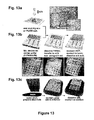
- FIGS. 13 a , 13 b and 13 c provide schematic illustrations and images corresponding to steps for fabricating silk-supported implantable biomedical devices. Schematic illustration and images corresponding to steps for fabricating conformal silk-supported Pl electrode arrays.
- a Casting and drying of silk fibroin solution on a temporary substrate of PDMS; 5-15 ⁇ m thick silk film after drying for 12 hours at room temperature.
- b Steps for fabricating the electrode arrays, transfer printing them onto silk, and connecting to ACF cable.
- c Schematic illustration of clinical usage of a representative device in an ultrathin mesh geometry with dissolvable silk support.
- FIGS. 14 a , 14 b and 14 c provide images of an implantable biomedical device fabrication process using a thick polyimide film. Electrode array fabrication process using thick PI film (Kapton, Dupont, USA). a, attach Pl film to PDMS coated glass. b, electrode array fabrication. c, ACF connection.
- FIGS. 15 a and 15 b provide images of implantable biomedical devices on silk and polyimide, respectively, after connection of anisotropic conductive film cables and circuit boards. Images of electrode array after connection of ACF and circuit board. a, electrode array with thin ( ⁇ 10 ⁇ m) substrate thickness. b, electrode array with thick (>10 ⁇ m) substrate thickness.
- FIGS. 16 a , 16 b , 16 c show time-dependent changes as a silk substrate dissolves. Time dependent changes as the silk substrate dissolves.
- a Dissolution of the silk via submersion in warm water.
- b Total bending stiffness of 7 ⁇ m and 2.5 ⁇ m electrode arrays on supporting silk films as a function of thickness of the supporting silk film; inset shows the ratio of bending stiffness between 7 ⁇ m and 2.5 ⁇ m.
- c Time dependent change in volume of a silk film during dissolution (left frame) and bending stiffness calculated for silk treated in 70% ethanol for 5 seconds for two different array thicknesses (right frame). The 5 second ethanol treatment increases the dissolution time from minutes to about 1 hour.
- FIG. 16 d shows The bending stiffness of the neural sensor of thickness 7 ⁇ m and 2.5 ⁇ m on a silk backing substrate.
- FIG. 17 shows time-dependent bending stiffness changes for 7 ⁇ m and 2.5 ⁇ m implantable biomedical devices.
- FIGS. 18 a , 18 b , 18 c and 18 d show photographs of neural implantable biomedical devices of varying thickness on simulated brain models. Neural electrode arrays of varying thickness on simulated brain models to illustrate flexibility.
- a Schematic illustration of trends in thickness and structure that improve conformal contact.
- b Series of pictures illustrating how the thickness of the electrode array contributes to conformal contact on a brain model.
- c Magnified view of these pictures.
- d Image of an electrode array with a mesh design on dissolvable silk substrate. Arrows indicate struts in the mesh that help to stabilize the Au interconnects after dissolution of the silk.
- the inset illustrates the high degree of conformal contact that can be achieved on the brain model once the silk substrate has been dissolved.
- FIG. 19 shows design parameters for a mesh electrode array.
- FIGS. 20 a and 20 b provide images of mesh implantable biomedical devices on a glass cylinder and a human brain model, respectively, after dissolution of a silk substrate.
- FIGS. 21 a , 21 b , 21 c , 21 d and 21 e provide images and graphs of mechanically modeled, theoretically predicted, and measured properties of implantable biomedical devices. Mechanical modeling, theoretical predictions and measured properties.
- a A thin film wrapped around a cylinder of radius R. The unwrapped and wrapped states appear in the top and center frames, respectively. The bottom frame compares the mechanics model and experiments.
- b A thin film wrapped around two overlapped cylinders. The top and center frames show the unwrapped and wrapped states, respectively.
- the bottom frame shows a comparison between the mechanics model and experiments.
- c Images of electrode arrays (76 ⁇ m sheet in left top, 2.5 ⁇ m sheet in right top and 2.5 ⁇ m mesh in bottom panel) wrapped onto a glass hemisphere.
- d Mechanics models for sheet (left frame) and mesh (right frame) designs.
- e The critical adhesion energy (left frame) and the normal (peeling) stress between the film and sphere surface (right frame) for sheet and mesh designs.
- FIGS. 22 a , 22 b , 22 c and 22 d provide images of wrapping experiments on glass cylinders of different diameters (diameter is a, 3.5 cm, b, 1.3 cm, c, 0.4 cm and d, 0.1 cm.)
- FIGS. 23 a and 23 b provide images of wrapping experiments on overlapped cylinders (a, angled view. b, side view).
- FIGS. 24 a and 24 b provide modeling results for the critical adhesion energy and normal (peeling) stress, respectively.
- a The critical adhesion energy for sheet and mesh designs.
- b The normal (peeling) stress between the film and sphere surface for sheet and mesh designs.
- FIGS. 25 a , 25 b , 25 c and 25 d provide photographs and data from animal validation experiments. Photographs and data from animal validation experiments. Image of electrode array on cat brain (left) and average evoked response from each electrode with the color showing the extent of cross-correlation between the evoked response on each electrode and an average of all the responses (right) for 75 ⁇ m a, 2.5 ⁇ m b and 2.5 ⁇ m mesh c electrode array. d, Representative voltage data from a single electrode in a 2.5 ⁇ m mesh electrode array showing a sleep spindle.
- FIGS. 26 a and 26 b provide schematic diagrams of implantable biomedical devices. Schematic diagram for analytical model and its modeling result. a, Cross section of the neural sensor, with geometrical parameters illustrated. b, Cross section of the neural sensor on a silk backing substrate.
- FIG. 27 shows the design of a circuit board.
- “Functional layer” refers to a layer that imparts some functionality to the device.
- the functional layer may contain semiconductor components.
- the functional layer may comprise multiple layers, such as multiple semiconductor layers separated by support layers.
- the functional layer may comprise a plurality of patterned elements, such as interconnects running between electrodes or islands.
- the functional layer may be heterogeneous or may have one or more properties that are inhomogeneous. “Inhomogeneous property” refers to a physical parameter that can spatially vary, thereby effecting the position of the neutral mechanical plane within a multilayer device.
- “Structural layer” refers to a layer that imparts structural functionality, for example by supporting and/or encapsulating device components.
- semiconductor refers to any material that is an insulator at a very low temperature, but which has an appreciable electrical conductivity at a temperature of about 300 Kelvin. In the present description, use of the term semiconductor is intended to be consistent with use of this term in the art of microelectronics and electronic devices.
- Useful semiconductors include those comprising elemental semiconductors, such as silicon, germanium and diamond, and compound semiconductors, such as group IV compound semiconductors such as SiC and SiGe, group III-V semiconductors such as AlSb, AlAs, AlN, AlP, BN, BP, BAs, GaSb, GaAs, GaN, GaP, InSb, InAs, InN, and InP, group III-V ternary semiconductors alloys such as Al x Ga 1-x As, group II-VI semiconductors such as CsSe, CdS, CdTe, ZnO, ZnSe, ZnS, and ZnTe, group I-VII semiconductors such as CuCl, group IV-VI semiconductors such as PbS, PbTe, and SnS, layer semiconductors such as PbI 2 , MoS 2 , and GaSe, oxide semiconductors such as CuO and Cu 2 O.
- group IV compound semiconductors such as SiC and SiGe
- semiconductor includes intrinsic semiconductors and extrinsic semiconductors that are doped with one or more selected materials, including semiconductors having p-type doping materials and n-type doping materials, to provide beneficial electronic properties useful for a given application or device.
- semiconductor includes composite materials comprising a mixture of semiconductors and/or dopants.
- Specific semiconductor materials useful for some embodiments include, but are not limited to, Si, Ge, Se, diamond, fullerenes, SiC, SiGe, SiO, SiO 2 , SiN, AlSb, AlAs, AlIn, AlN, AlP, AlS, BN, BP, BAs, As 2 S 3 , GaSb, GaAs, GaN, GaP, GaSe, InSb, InAs, InN, InP, CsSe, CdS, CdSe, CdTe, Cd 3 P 2 , Cd 3 As 2 , Cd 3 Sb 2 , ZnO, ZnSe, ZnS, ZnTe, Zn 3 P 2 , Zn 3 As 2 , Zn 3 Sb 2 , ZnSiP 2 , CuCl, PbS, PbSe, PbTe, FeO, FeS 2 , NiO, EuO, EuS, PtSi, TlBr, CrBr 3
- Impurities of semiconductor materials are atoms, elements, ions and/or molecules other than the semiconductor material(s) themselves or any dopants provided to the semiconductor material. Impurities are undesirable materials present in semiconductor materials which may negatively impact the electronic properties of semiconductor materials, and include but are not limited to oxygen, carbon, and metals including heavy metals. Heavy metal impurities include, but are not limited to, the group of elements between copper and lead on the periodic table, calcium, sodium, and all ions, compounds and/or complexes thereof.
- a “semiconductor component” broadly refers to any semiconductor material, composition or structure, and expressly includes high quality single crystalline and polycrystalline semiconductors, semiconductor materials fabricated via high temperature processing, doped semiconductor materials, inorganic semiconductors, and composite semiconductor materials.
- a “component” is used broadly to refer to an individual part of a device.
- An “interconnect” is one example of a component, and refers to an electrically conducting structure capable of establishing an electrical connection with another component or between components. In particular, an interconnect may establish electrical contact between components that are separate. Depending on the desired device specifications, operation, and application, an interconnect is made from a suitable material. Suitable conductive materials include semiconductors.
- TFTs thin film transistors
- Other components include, but are not limited to, thin film transistors (TFTs), transistors, electrodes, integrated circuits, circuit elements, control elements, microprocessors, transducers, islands, bridges and combinations thereof.
- Components may be connected to one or more contact pads as known in the art, such as by metal evaporation, wire bonding, and application of solids or conductive pastes, for example.
- NMP Neuro mechanical plane
- the NMP is less susceptible to bending stress than other planes of the device that lie at more extreme positions along the vertical, h, axis of the device and/or within more bendable layers of the device.
- the position of the NMP is determined by both the thickness of the device and the materials forming the layer(s) of the device.
- Coupled refers to the relative position of two or more objects, planes or surfaces, for example a surface such as a neutral mechanical plane that is positioned within or is adjacent to a layer, such as a functional layer, substrate layer, or other layer.
- a neutral mechanical plane is positioned to correspond to the most strain-sensitive layer or material within the layer.
- “Proximate” refers to the relative position of two or more objects, planes or surfaces, for example a neutral mechanical plane that closely follows the position of a layer, such as a functional layer, substrate layer, or other layer while still providing desired conformability without an adverse impact on the strain-sensitive material physical properties.
- Stress-sensitive refers to a material that fractures or is otherwise impaired in response to a relatively low level of strain. In general, a layer having a high strain sensitivity, and consequently being prone to being the first layer to fracture, is located in the functional layer, such as a functional layer containing a relatively brittle semiconductor or other strain-sensitive device element.
- a neutral mechanical plane that is proximate to a layer need not be constrained within that layer, but may be positioned proximate or sufficiently near to provide a functional benefit of reducing the strain on the strain-sensitive device element when the device is conformed to a tissue surface.
- Electrode generally refers to a device incorporating a plurality of components, and includes large area electronics, printed wire boards, integrated circuits, component arrays, biological and/or chemical sensors, and physical sensors (e.g., temperature, etc.).
- Sensing refers to detecting the presence, absence, amount, magnitude or intensity of a physical and/or chemical property.
- Useful electronic device components for sensing include, but are not limited to electrode elements, chemical or biological sensor elements, pH sensors, temperature sensors and capacitive sensors.
- Actuating refers to stimulating, controlling, or otherwise affecting an external structure, material or fluid, for example a biological tissue.
- Useful electronic device components for actuating include, but are not limited to, electrode elements, electromagnetic radiation emitting elements, light emitting diodes, lasers, and heating elements.
- Island refers to a relatively rigid component of an electronic device comprising a plurality of semiconductor components. “Bridge” refers to structures interconnecting two or more islands or one island to another component. Specific bridge structures include semiconductor interconnects.
- Encapsulate refers to the orientation of one structure such that it is at least partially, and in some cases completely, surrounded by one or more other structures. “Partially encapsulated” refers to the orientation of one structure such that it is partially surrounded by one or more other structures. “Completely encapsulated” refers to the orientation of one structure such that it is completely surrounded by one or more other structures.
- the invention includes implantable devices having partially or completely encapsulated inorganic semiconductor components and/or electrodes.
- Barrier layer refers to a component spatially separating two or more other components or spatially separating a component from a structure, material or fluid external to the device.
- a barrier layer encapsulates one or more components.
- a barrier layer separates one or more components from an aqueous solution, a biological tissue or both.
- a barrier layer(s), and optionally a sacrificial layer on a substrate may be etched to produce a “mesh structure”, where at least a portion of the barrier layer(s), and optionally the sacrificial layer on a substrate, is removed. For example a portion of the barrier layer(s) disposed approximately 10 nanometers or more from an inorganic semiconductor component or additional component is removed. Removal of at least a portion of the barrier layer(s), and optionally the sacrificial layer on the substrate, may produce (i) one or more holes within the barrier layer(s) and/or (ii) electrical components, which are physically joined by a barrier layer(s) at a proximal end and physically separated at a distal end.
- a mesh structure may be disposed upon a contiguous bioresorbable substrate, which provides structural support for the device during deployment into a biological environment.
- Contiguous refers to materials or layers that are touching or connected throughout in an unbroken sequence.
- a contiguous layer of an implantable biomedical device has not been etched to remove a substantial portion (e.g., 10% or more) of the originally provided material or layer.
- Active circuit and “active circuitry” refer to one or more components configured for performing a specific function.
- Useful active circuits include, but are not limited to, amplifier circuits, multiplexing circuits, current limiting circuits, integrated circuits, transistors and transistor arrays.
- Substrate refers to a material, layer or other structure having a surface, such as a receiving surface, that is capable of supporting one or more components or electronic devices.
- a component that is “bonded” to the substrate refers to a component that is in physical contact with the substrate and unable to substantially move relative to the substrate surface to which it is bonded. Unbonded components or portions of a component, in contrast, are capable of substantial movement relative to the substrate.
- Bioresorbable refers to a material that is susceptible to being chemically broken down into lower molecular weight chemical moieties by reagents that are naturally present in a biological environment. In an in-vivo application, the chemical moieties may be assimilated into human or animal tissue.
- a bioresorbable material that is “substantially completely” resorbed is highly resorbed (e.g., 95% resorbed, or 98% resorbed, or 99% resorbed, or 99.9% resorbed, or 99.99% resorbed), but not completely (i.e., 100%) resorbed.
- Biocompatible refers to a material that does not elicit an immunological rejection or detrimental effect when it is disposed within an in-vivo biological environment.
- a biological marker indicative of an immune response changes less than 10%, or less than 20%, or less than 25%, or less than 40%, or less than 50% from a baseline value when a biocompatible material is implanted into a human or animal.
- Bioinert refers to a material that does not elicit an immune response from a human or animal when it is disposed within an in-vivo biological environment. For example, a biological marker indicative of an immune response remains substantially constant (plus or minus 5% of a baseline value) when a bioinert material is implanted into a human or animal.
- Nanostructured contact surface and “microstructured contact surface” refer to device surfaces having nanometer-sized and micrometer-sized relief features, respectively, for contacting and penetrating a target tissue and improving adhesion between the implantable biomedical device and the target tissue.
- the relief features extend a length, x, from a substantially contiguous plane of the device surface.
- Quantitative descriptors of a structured contact surface include surface roughness parameters, such as R max , R a , and normalized roughness (R a /R max ), all of which may be measured by atomic force microscopy (AFM).
- R max is the maximum height between a highest peak to a lowest valley.
- R a is the center-line-mean roughness, which is the average of an absolute value of a deviation from a center line of a roughness curve to the roughness curve.
- the surface of a substrate or barrier layer is “substantially smooth”, for the purposes of this disclosure, if the surface has an R a value of 100 nm or less. If the surface has an R a value greater than 100 nm, the surface is considered to be a “structured surface” for purposes of this disclosure.
- a structured surface may contain at leastone feature selected from the group consisting of barbs, spikes, protrusions and any combination of these.
- Dielectric refers to a non-conducting or insulating material.
- an inorganic dielectric comprises a dielectric material substantially free of carbon.
- Specific examples of inorganic dielectric materials include, but are not limited to, silicon nitride, silicon dioxide and polymers.
- Polymer refers to a macromolecule composed of repeating structural units connected by covalent chemical bonds or the polymerization product of one or more monomers, often characterized by a high molecular weight.
- the term polymer includes homopolymers, or polymers consisting essentially of a single repeating monomer subunit.
- the term polymer also includes copolymers, or polymers consisting essentially of two or more monomer subunits, such as random, block, alternating, segmented, grafted, tapered and other copolymers.
- Useful polymers include organic polymers or inorganic polymers that may be in amorphous, semi-amorphous, crystalline or partially crystalline states. Crosslinked polymers having linked monomer chains are particularly useful for some applications.
- Polymers useable in the methods, devices and components include, but are not limited to, plastics, elastomers, thermoplastic elastomers, elastoplastics, thermoplastics and acrylates.
- Exemplary polymers include, but are not limited to, acetal polymers, biodegradable polymers, cellulosic polymers, fluoropolymers, nylons, polyacrylonitrile polymers, polyamide-imide polymers, polyimides, polyarylates, polybenzimidazole, polybutylene, polycarbonate, polyesters, polyetherimide, polyethylene, polyethylene copolymers and modified polyethylenes, polyketones, poly(methyl methacrylate), polymethylpentene, polyphenylene oxides and polyphenylene sulfides, polyphthalamide, polypropylene, polyurethanes, styrenic resins, sulfone-based resins, vinyl-based resins, rubber (including natural rubber, styrene-butadiene,
- Elastomeric stamp and “elastomeric transfer device” are used interchangeably and refer to an elastomeric material having a surface that can receive as well as transfer a material.
- Exemplary elastomeric transfer devices include stamps, molds and masks. The transfer device affects and/or facilitates material transfer from a donor material to a receiver material.
- Elastomer refers to a polymeric material which can be stretched or deformed and returned to its original shape without substantial permanent deformation. Elastomers commonly undergo substantially elastic deformations. Useful elastomers include those comprising polymers, copolymers, composite materials or mixtures of polymers and copolymers. Elastomeric layer refers to a layer comprising at least one elastomer. Elastomeric layers may also include dopants and other non-elastomeric materials.
- elastomers include, but are not limited to, thermoplastic elastomers, styrenic materials, olefinic materials, polyolefin, polyurethane thermoplastic elastomers, polyamides, synthetic rubbers, PDMS, polybutadiene, polyisobutylene, poly(styrene-butadiene-styrene), polyurethanes, polychloroprene and silicones.
- an elastomeric stamp comprises an elastomer.
- Exemplary elastomers include, but are not limited to silicon containing polymers such as polysiloxanes including poly(dimethyl siloxane) (i.e.
- PDMS and h-PDMS poly(methyl siloxane), partially alkylated poly(methyl siloxane), poly(alkyl methyl siloxane) and poly(phenyl methyl siloxane), silicon modified elastomers, thermoplastic elastomers, styrenic materials, olefinic materials, polyolefin, polyurethane thermoplastic elastomers, polyamides, synthetic rubbers, polyisobutylene, poly(styrene-butadiene-styrene), polyurethanes, polychloroprene and silicones.
- a polymer is an elastomer.
- Conformable refers to a device, material or substrate which has a bending stiffness that is sufficiently low to allow the device, material or substrate to adopt any desired contour profile, for example a contour profile allowing for conformal contact with a surface having a pattern of relief features.
- a desired contour profile is that of a tissue in a biological environment.
- Conformal contact refers to contact established between a device and a receiving surface, which may for example be a target tissue in a biological environment.
- conformal contact involves a macroscopic adaptation of one or more surfaces (e.g., contact surfaces) of an implantable device to the overall shape of a tissue surface.
- conformal contact involves a microscopic adaptation of one or more surfaces (e.g., contact surfaces) of an implantable device to a tissue surface resulting in an intimate contact substantially free of voids.
- conformal contact involves adaptation of a contact surface(s) of the implantable device to a receiving surface(s) of a tissue such that intimate contact is achieved, for example, wherein less than 20% of the surface area of a contact surface of the implantable device does not physically contact the receiving surface, or optionally less than 10% of a contact surface of the implantable device does not physically contact the receiving surface, or optionally less than 5% of a contact surface of the implantable device does not physically contact the receiving surface.
- Young's modulus is a mechanical property of a material, device or layer which refers to the ratio of stress to strain for a given substance. Young's modulus may be provided by the expression:
- E Young's modulus
- L 0 the equilibrium length
- ⁇ L the length change under the applied stress
- F the force applied
- A the area over which the force is applied.
- Young's modulus may also be expressed in terms of Lame constants via the equation:
- High Young's modulus (or “high modulus”) and low Young's modulus (or “low modulus”) are relative descriptors of the magnitude of Young's modulus in a given material, layer or device.
- a high Young's modulus is larger than a low Young's modulus, preferably about 10 times larger for some applications, more preferably about 100 times larger for other applications, and even more preferably about 1000 times larger for yet other applications.
- a low modulus layer has a Young's modulus less than 100 MPa, optionally less than 10 MPa, and optionally a Young's modulus selected from the range of 0.1 MPa to 50 MPa.
- a high modulus layer has a Young's modulus greater than 100 MPa, optionally greater than 10 GPa, and optionally a Young's modulus selected from the range of 1 GPa to 100 GPa.
- “Inhomogeneous Young's modulus” refers to a material having a Young's modulus that spatially varies (e.g., changes with surface location).
- a material having an inhomogeneous Young's modulus may optionally be described in terms of a “bulk” or “average” Young's modulus for the entire material.
- Low modulus refers to materials having a Young's modulus less than or equal to 10 MPa, less than or equal to 5 MPa or less than or equal to 1 MPa.
- Bending stiffness is a mechanical property of a material, device or layer describing the resistance of the material, device or layer to an applied bending moment. Generally, bending stiffness is defined as the product of the modulus and area moment of inertia of the material, device or layer. A material having an inhomogeneous bending stiffness may optionally be described in terms of a “bulk” or “average” bending stiffness for the entire layer of material.
- implantable biomedical devices for sensing a parameter associated with a target tissue and/or actuating a target tissue in a biological environment, as well as methods for making and using the implantable biomedical devices. These devices are capable of intimate integration on the soft, curvilinear surfaces of biological tissues and are useful for monitoring and/or treating medical conditions in real time and with high spatial precision.
- the disclosed devices and methods also include those specially suited for monitoring and/or actuating tissues in-vivo.
- the approaches rely on dissolvable, biocompatible, and bioresorbable substrates, where dissolution and capillary forces drive a wrapping process. Purely passive electrode systems serve to demonstrate the advantages and underlying aspects of these systems, but the same approaches are compatible with fully active electronics and optoelectronics.
- Implantable biomedical devices and methods of making and using the devices will now be described with reference to the figures. For clarity, multiple items within a figure may not be labeled and the figures may not be drawn to scale. Like numerals in multiple figures represent like items, and items numbered with parentheses, e.g., implantable biomedical devices 100 ( 1 )- 100 ( 7 ), represent species within a genus, which may be broadly referred to without parentheses, e.g., implantable biomedical device 100 .
- FIG. 1 a shows a top plan view of an implantable biomedical device 100 ( 1 ) having a plurality of electronic interconnects 106 and electrodes 108 , which form part of an electronic device, disposed upon or encapsulated within a barrier layer 104 ( 1 ) that is supported by a bioresorbable substrate 102 ( 1 ).
- Connection of an anisotropic conductive film (ACF) cable 110 to implantable biomedical device 100 ( 1 ) allows for communication with a circuit board 112 , which may be used in conjunction with known software, memory devices, user interfaces, and power sources (not shown) to analyze data obtained from device 100 ( 1 ) and/or to deliver electromagnetic radiation to device 100 ( 1 ).
- FIG. 1 a shows a top plan view of an implantable biomedical device 100 ( 1 ) having a plurality of electronic interconnects 106 and electrodes 108 , which form part of an electronic device, disposed upon or encapsulated within a barrier layer 104 ( 1 ) that is supported by
- FIG. 1 b shows a cross-sectional view of implantable biomedical device 100 ( 1 ) taken through a plane defined by line B-B.
- Interconnects 106 are shown as encapsulated within barrier layer 104 ( 1 ) and coincident to a neutral mechanical plane (NMP) of the device.
- FIG. 1 c shows a cross-sectional view of implantable biomedical device 100 ( 1 ) taken through a plane defined by line C-C.
- Interconnects 106 remain disposed within barrier layer 104 ( 1 ), but electrodes 108 are shown as exposed to ambient conditions. In other embodiments (not shown), the entire electronic device including electrodes 108 may be encapsulated within a barrier layer.
- FIG. 2 provides a top perspective view of implantable biomedical device 100 ( 1 ) having physical dimensions including a vertical dimension or height, h, a lateral dimension or width, b, and a longitudinal dimension or length, L.
- Implantable biomedical device 100 ( 1 ) may have any regular or irregular shape, but will often be in the form of a square or rectangular parallelogram.
- FIG. 3 shows a top plan view of an implantable biomedical device 100 ( 2 ) having islands 302 and bridges 304 , which form part of an electronic device.
- Islands 302 and bridges 304 are at least partially encapsulated by a barrier layer 104 ( 2 ) and supported by a bioresorbable substrate 102 ( 2 ).
- Islands 302 may, for example, be rigid semiconductor components linked by bridges 304 , which may have a wavy, serpentine or meandering configuration that allows for a high degree of flexibility, bendability, conformability or compressibility.
- Bridges 304 may be disposed completely within the plane of the islands or at least a portion of bridges 304 may extend vertically above the plane of the islands, such that a void space exists beneath at least part of each bridge 304 .
- FIG. 4 shows a side plan view of an implantable biomedical device 100 ( 3 ) having a biocompatible layer 402 in addition to a bioresorbable substrate 102 ( 3 ), a barrier layer 104 ( 3 ) and electronic device components 404 , such as interconnects, electrodes, islands, bridges, etc.
- FIGS. 5 a and 5 b provide schematic illustrations of implantable biomedical devices 100 ( 4 ) and 100 ( 5 ) having mesh structures.
- FIG. 5 a shows an electronic device having a tentacle mesh structure, where semiconductor components 502 are at least partially encapsulated by a barrier layer and/or biocompatible layer 508 .
- Layer 508 physically joins proximal ends 504 of semiconductor components 502 , but distal ends 506 of semiconductor components 502 are physically separated.
- each semiconductor component 502 is separated from every other semiconductor component at its distal end 506 .
- groups of two or more semiconductor components 502 may be physically separated from other groups of neighboring semiconductor components 502 .
- a bioresorbable substrate 102 ( 4 ) provides support for the mesh electronic device.
- FIG. 5 b shows an electronic device having a perforated mesh structure, where semiconductor components in the form of islands 302 and bridges 304 are at least partially encapsulated by a barrier layer and/or biocompatible layer 510 .
- Layer 510 contains holes 512 where the material of layer 510 has been removed, e.g., by reactive ion etching.
- a bioresorbable substrate 102 ( 5 ) provides support for the mesh electronic device.
- Perforated mesh structures are not limited to electronic devices comprising islands and bridges. Barrier and/or biocompatible layer material may be removed to form holes in any of the electronic devices described herein. For example, etching of implantable biomedical device 100 ( 4 ) ( FIG. 5 a ) that removes material between semiconductor components 502 but leaves both proximal 504 and distal 506 ends joined will create a perforated mesh structure.
- FIG. 6 provides a flowchart 600 illustrating exemplary steps for making implantable biomedical devices 100 having a mesh structure, e.g., 100 ( 4 ) and 100 ( 5 ).
- a sacrificial layer is provided on a substrate.
- a first dielectric layer is applied to the sacrificial layer on a substrate in step 606 , and at least one inorganic semiconductor component is positioned or otherwise assembled on the first dielectric layer in step 608 .
- a portion of the at least one inorganic semiconductor component is covered with a second dielectric layer, in step 610 , to generate a covered inorganic semiconductor component having an exposed distal end.
- an electrode is positioned to physically contact the exposed distal end of the inorganic semiconductor component.
- a portion of the first and second dielectric layers is then removed to generate a mesh structure in step 614 .
- the sacrificial layer on the substrate is removed (e.g., dissolved or etched), in step 616 , to leave a substantially substrate-free, mesh structure.
- the substantially substrate-free, mesh structure is transferred to a bioresorbable substrate in step 618 , for example using transfer printing, such as dry contact transfer printing.
- FIG. 7 provides a flowchart 700 illustrating exemplary steps for implanting a biomedical device 100 , and optionally using the implanted biomedical device to actuate a target tissue and/or sense a parameter associated with the target tissue.
- an implantable biomedical device 100 is provided.
- the implantable biomedical device is then contacted, in step 706 , with a target tissue in a biological environment and a bioresorbable substrate of the implantable biomedical device is at least partially resorbed to establish conformal contact between the implantable biomedical device and the target tissue, in step 708 .
- the target tissue is actuated.
- a voltage, electromagnetic radiation or current may be generated at a surface of the target tissue, in optional step 712 .
- a parameter associated with the target tissue may be sensed.
- a voltage, electromagnetic radiation or current may be measured at a surface of the target tissue, in optional step 716 .
- Steps 710 and 712 for actuating the target tissue and steps 714 and 716 for sensing a parameter associated with the tissue are not mutually exclusive.
- a portion of semiconductor components of an implantable biomedical device may actuate the target tissue while another portion senses parameters associated with the target tissue.
- all the semiconductor components of an implantable biomedical device may alternately sense and actuate, e.g., in accordance with a feedback loop.
- FIGS. 8 a and 8 b show side plan views of implantable biomedical devices 100 ( 6 ) and 100 ( 7 ) having planar contact surfaces 802 and nanostructured or microstructured contact surfaces 804 , respectively.
- barrier layer 104 interfaces with the target tissue.
- bioresorbable substrate 102 may interface with the target tissue, and bioresorbable substrate 102 may be planar or structured.
- Structured contact surfaces 804 have nanometer-sized or micrometer-sized relief features 806 , such as barbs 808 , spikes 810 , and protrusions 812 , which may extend a length, x, from a surface of implantable biomedical device 100 ( 7 ).
- implantable biomedical devices advantageously utilize silk as a bioresorbable substrate.
- Silk is biocompatible, FDA-approved, optically transparent, mechanically robust (high mechanical modulus and toughness), and flexible in thin film form. It is also compatible with aqueous processing, which preserves sensitive electronic functions, and amenable to chemical and biological functionalization. The presence of diverse amino acid side chains facilitates coupling chemistry for functionalizing silks.
- Silk is also water soluble with programmable rates of proteolytic biodegradation (yielding non-inflammatory amino acids) over a range from minutes to hours to years.
- Some other natural polymers that exhibit properties similar to or analogous to silk include, but are not limited to, chitosan, collagen, gelatin, agarose, chitin, polyhydroxyalkanoates, pullan, starch (amylose amylopectin), cellulose, hyaluronic acid, or any combination of these.
- Silk may be obtained from various natural sources, for example, from the silkworm Bombyx mori or from the spider Nephila clavipes .
- Silk solutions used in accordance with embodiments of the present invention may be obtained, for example, from a solution containing a dissolved silkworm silk (e.g. from Bombyx mori ), a dissolved spider silk (e.g. from Nephila clavipes ), or from a solution containing a recombinant silk, such as from bacteria, yeast, mammalian cells, transgenic animals, or transgenic plants.
- the silk of the bioresorbable substrate may be silk fibroin protein, which consists of layers of antiparallel beta sheets and has a primary structure consisting mainly of the recurrent amino acid sequence (Gly-Ser-Gly-Ala-Gly-Ala) n .
- Fibroin is known to arrange itself in three structures, called silk I, II, and III.
- Silk I is the natural, amorphous form of fibroin, as emitted from the Bombyx mori silk glands.
- Silk II refers to the crystalline arrangement of fibroin molecules in spun silk, which has greater strength.
- Silk III is formed principally in solutions of fibroin at an interface (i.e. air-water interface, water-oil interface, etc.). In the disclosed implantable biomedical devices, silk I, II and/or III may be used.
- Silk substrates were typically prepared from material derived from Bombyx mori cocoons, according to published procedures. See, Sofia, S., McCarthy, M. B., Gronowicz, G. & Kaplan, D. L. Functionalized silk-based biomaterials for bone formation. J. Biomed. Mater. Res. 54, 139-148 (2001); Perry, H., Gopinath, A., Kaplan, D. L., Negro, L. D. & Omenetto, F. G. Nano- and micropatterning of optically transparent, mechanically robust, biocompatible silk fibroin films. Adv. Mater. 20, 3070-3072 (2008); and WO 2008/108838.
- silk solutions may be prepared using organic solvents, as described in WO 2008/108838 which is hereby incorporated by reference in its entirety.
- organic solvents used in the preparation of silk materials can alter the biocompatibility and physical properties of silk materials. For example, immersion of silk films in organic solvents, such as methanol, may cause dehydration of the hydrated or swollen structure, leading to crystallization and, thus, loss of solubility in water. Further, the use of organic solvents can render the silk material less degradable.
- the presence of organic solvents, as compared to aqueous solvents, in the silk solution may generate silk substrates with more crystalline structures, as compared to amorphous structures. This phenomenon may be used to control, for example, the rate of bioresorption of the silk. Accordingly, depending on the desired resorption rate, the silk solution may be prepared using any suitable ratio of aqueous:organic solution, for example, 100% aqueous, about 80% aqueous, about 60% aqueous, about 50% aqueous, about 40% aqueous, about 20% aqueous, or about 10% aqueous.
- Additional techniques may be used to control the bioresorption rate of the silk substrate.
- the rate at which resorption occurs may be tailored by altering: substrate material, substrate thickness, crosslinking, the extent of inter-chain hydrogen bonding or Van der Weals forces, and/or molecular alignment (e.g., via mono-axial or bi-axial stretching, spinning into fiber, and/or weaving).
- bioresorbable polymers including, but not limited to, a biopolymer, a synthetic polymer, a protein, a polysaccharide, poly(glycerol-sebacate) (PGS), polydioxanone, poly(lactic-co-glycolic acid) (PLGA), polylactic acid (PLA), collagen, chitosan, or any combination of these, may be used alone as the bioresorbable substrate or may be added to the silk solution to generate composite silk substrates.
- a substrate comprises from about 50 to about 99.99 parts by volume (vol %) silk protein solution and from about 0.01 to about 50 vol % additional polymer.
- implantable biomedical devices described herein may be used for drug delivery.
- one or more therapeutic agents may be encapsulated within the substrate material as a liquid, a gel, a dispersed solid, or any other appropriate physical form, to be administered to a patient upon resorption of the substrate.
- the silk or other bioresorbable polymer solution may be mixed with one or more therapeutic agents, and optionally a pharmaceutically acceptable carrier, prior to forming the substrate. Any pharmaceutical carrier that does not dissolve the bioresorbable material may be used.
- implantable biomedical devices of the invention are used to administer, deliver and/or activate a therapeutic agent provided to a subject.
- the bioresorbable substrate is a multifunctional component that releases a therapeutic agent upon administration to a biological environment and/or contact with a target tissue.
- the invention includes, for example, bioresorbable substrates having embedded therapeutic agents, such as drugs (e.g., small molecule therapeutics), nanoparticles and/or biomolecules, such as proteins, peptides, oligonucleotides (e.g., DNA or RNA), etc.
- This aspect of the present invention may be useful for a range of therapeutic applications including controlled release of therapeutic agents and/or targeted administration of therapeutic agents to a selected tissue type.
- the invention includes implantable devices and systems wherein the electronic device component mediates release of therapeutic agent from the bioresorbable substrate via thermal means, for example by local heating of components of the implantable device, such as the bioresorbable substrate.
- the invention includes implantable devices and systems wherein the electronic device component mediates release of therapeutic agent from the bioresorbable substrate via processes driven by generation and control of local electric fields, such as electrophoresis processes for the release of proteins or peptides.
- the invention includes implantable devices and systems wherein the electronic device component mediates release and/or activation of a therapeutic agent from the bioresorbable substrate via processes driven by absorption of electromagnetic radiation.
- the implantable device includes an electronic device component, such as a laser or LED array, capable of optically activating a therapeutic agent during and/or upon release from the bioresorbable substrate. This aspect of the invention is useful for therapeutic applications including phototherapy.
- Therapeutic agents that may be used in conjunction with the devices described herein include, but are not limited to: small molecules; proteins; peptides; nucleotides; nucleic acids; carbohydrates; simple sugars; cells; genes; anti-thrombotics; anti-metabolics; anticoagulants; antimitotics; fibrinolytics; anti-inflammatory steroids; monoclonal antibodies; vitamins; sedatives; steroids; hypnotics; antiinfectives, such as antibiotics and antiviral agents; chemotherapeutic agents (i.e., anticancer agents); prostaglandins, radiopharmaceuticals, anti-rejection agents; analgesics; anti-inflammatory agents; hormones, such as steroids; growth factors (inhibitors and promoters), such as epidermal growth factor, fibroblast growth factor, platelet-derived growth factor, insulin-like growth factor, transforming growth factors, and vascular endothelial growth factor; anti-angiogenic proteins such as endostatin; polysaccharides; glycoproteins; lipoprotein
- a therapeutic agent circulating through an in-vivo biological environment may be activated when it receives electromagnetic radiation from a biomedical device implanted at a therapeutic site.
- electromagnetic radiation from a biomedical device implanted at a therapeutic site.
- energy within the ultraviolet and visible regions of the electromagnetic spectrum may be useful.
- Advanced implantable bioMedical devices have great potential in clinical applications. Systems that allow insertion into the body to establish conformal contact with the curvilinear surfaces of various organs must be flexible and biocompatible. The conformal and flexible characteristics could be enabled by recently reported organic, inorganic, and nanomaterial based electronics. Achieving biocompatibility, on the other hand, can be challenging, due to the complex nature of the biological response to many organic and inorganic materials. An ideal solution to this problem that largely avoids the longer term issues involves the construction of the electronics out of materials that are soluble and biodegradable; here the device simply disappears, or resorbs, over time.
- a large fraction of the device can be designed to resorb, such that a sufficiently small amount of material remains that its induced biological response is negligible.
- This approach has the advantage that it does not require the development of an entire set of biodegradable electronic materials, but still yields an overall system that dissipates bulk material features at a rate suitable for the application.
- This example describes the combination of silicon electronics, based on nanomembranes of silicon, with biodegradable thin film substrates of silk protein, to yield a flexible system and device that is largely resorbable in the body.
- the use of silicon provides high performance, good reliability, and robust operation.
- Silk is attractive, compared to other biodegradable polymers such as poly(glycolic acid), poly(L-lactic acid), and collagen, because of its robust mechanical properties, the ability to tailor the dissolution, and/or biodegradation rates from hours to years, the formation of noninflammatory amino acid degradation products, and the option to prepare the materials at ambient conditions to preserve sensitive electronic functions
- FIG. 9 shows the schematic fabrication process.
- Single crystalline nanomembranes of silicon (thickness ⁇ 260 nm p-type, SOITEC, France) were used to construct transistors on ultrathin sheets of polyimide (Pl).
- the doped silicon nanomembranes were transfer printed onto a film of Pl (Pl, ⁇ 1.2 ⁇ m, Sigma Aldrich, USA) cast onto a thin sacrificial layer of poly(methylmethacrylate) (PMMA, ⁇ 100 nm, A2 PMMA, MicroChem, USA) on a silicon wafer (i.e., carrier wafer for processing).
- Pl poly(methylmethacrylate)
- Transfer printing delivered the devices to either a spin cast film of silk on a silicon substrate ( FIG. 9( c )) or a freestanding silk membrane ( FIG. 9( d )).
- a ⁇ 7% aqueous silk solution was spin coated on the backsides of the devices while on the PDMS stamp, at spin rates between 2000 and 3000 rpm for 30 s.
- This layer of silk served as an adhesive for a transfer, which involves first establishing conformal contact with the silk substrate while on a hot plate ( ⁇ 110° C.) and then slowly retrieving the stamp.
- This process yielded a system in which the substrate is water soluble, and resorbable, but the devices are not, as shown in the schematic diagram in FIG.
- the devices can be constructed in very small dimensions (interconnected or not, depending on the application), with very small total amounts of material, thereby offering the possibility to minimize their effects on the biology. Further, the mode of processing the silk can be designed to yield rapid dissolution rates, as is the case here, or to degrade over years.
- FIG. 10( a ) shows a freestanding silk film with transfer printed silicon devices.
- the center and right frames of FIG. 10( a ) demonstrate the mechanical flexibility of the system. Under bending at these levels (radius of curvature, R, as ⁇ 5 mm), no mechanical or adhesive failure was observed. It is estimated that the bend induced strains at the top surface of the silk film ( ⁇ 25 ⁇ m, ⁇ 5 mm bending radius) are in the range of ⁇ 0.25%. Electrical measurements of a typical n channel device show expected properties (solid line of FIG. 10( b )). Here, the channel length and width was 13 and 100 ⁇ m, respectively, and the gate oxide thickness was 50 nm.
- the electron mobility, threshold voltage, and on/off ratio calculated from the transfer curve in the left frame of FIG. 10( b ) are ⁇ 500 cm 2 /V s, ⁇ 0.2 V, and >10 4 , respectively.
- the current-voltage characteristics at different gate biases are shown in the right frame of FIG. 10( b ).
- the gate leakage current was less than tens of picoamperes.
- the nMOS transistor was characterized after dissolving the silk substrate in water and then filtering out the devices onto filter paper (dotted line of FIG. 10( b )). Even after dissolution, the transistors functioned with only modest changes in properties.
- the electron mobility, threshold voltage, and on/off ratio were estimated from the transfer curves to be ⁇ 440 cm 2 /V s, ⁇ 0.5 V, and >10 4 .
- This dissolution process relies on the capability of silk to disintegrate in water, leaving proteins as the products that are then degraded by proteolytic activity.
- the resulting silk fibroin protein is a Food and Drug Administration (FDA) approved biocompatible material that generates noninflammatory amino acid degradation products usable in cell metabolic functions.
- FDA Food and Drug Administration
- the mechanical properties of the silk substrate can be tailored, based on the mode of processing, to match the level of toughness required. To illustrate the process, images were collected at various times after dipping a typical device into a petri dish filled with water, at room temperature. With a ⁇ 25 ⁇ m thick silk substrate, complete dissolution within 3 min was observed, as shown in FIGS. 11( a ) and 11 ( b ).
- 11( c ) shows devices recovered onto a piece of filter paper. Since the vast majority of this type of implantable device consists of the substrate and because the sizes of the active devices can be reduced even further by using standard microelectronic technology, very tiny or negligible residues of nonresorbable materials can remain after dissolution.
- mice did not exhibit any sign of abscessing or liquid buildup, and initial integration of the silk carrier into the subcutaneous layers could be observed.
- the size of the implant is estimated to be between 15%-20% smaller than the originally implanted device and detachment of a few transistor structures can be observed, as shown in the right frame of FIG. 12 . Although additional studies are required, these initial in vivo tests suggest some promise for this form of biodegradable electronics.
- Penetrating microelectrode arrays consisting of sharp pins (typically, 10 ⁇ 10 arrays of pins with base widths ⁇ 80 ⁇ m, lengths ⁇ 1.5 mm and pitch ⁇ 400 ⁇ m) that connect to flat platforms for conventional wafer-based electronics are valuable for research in BCI, but they damage the tissue and do not offer long-term electrical interface stability. Comparable BCI performance can be achieved with non-penetrating, surface electrode systems that are minimally-invasive and provide greatly improved stability. Standard clinical subdural electrode arrays are useful for BCI but their widely spaced ( ⁇ 1 cm), large contact electrodes ( ⁇ 0.35 cm diameter) spatially undersample the electrical signals present on the surface of the brain. Decreasing the spacing and size of the measurement points can improve BCI performance by providing access to high temporal and spatial frequency signals. Such designs, however, demand excellent conformal coverage over the highly convoluted brain surface to ensure direct coupling between the brain surface and the electrodes.
- Silk is an appealing biopolymer for this application because it is optically transparent, mechanically robust and flexible in thin film form, compatible with aqueous processing, amenable to chemical and biological functionalization, and it is biocompatible, bioresorbable, and water soluble with programmable rates of dissolution.
- the ability of silk films to serve as a platform for transistors and various classes of photonic devices has been demonstrated.
- the process for preparing silk substrates for the purposes reported here began with material derived from Bombyx mori cocoons, and followed published procedures. Briefly, boiling the cocoons in a 0.02 M aqueous solution of sodium carbonate for 60 minutes removed sericin, a water-soluble glycoprotein that binds fibroin filaments in the cocoon but can induce undesirable immunological responses.
- polyimide served as a support for arrays of electrodes designed for passive neural recording.
- Control devices consisted of otherwise similar layouts, but formed using standard photolithographic procedures applied directly on commercial Pl films (Kapton, DuPont) with thicknesses of 25 and 75 ⁇ m ( FIG. 14 ).
- Anisotropic conductive film (ACF) bonded to electrode pads at one end of the arrays provided electrical connection to the external data acquisition system ( FIG. 15 ).
- Ultrathin Pl films, with or without mesh layouts, cannot be manipulated effectively for processing, interconnecting or implanting onto the brain due to their extreme flexibility and mechanical fragility.
- the fabrication process exploited layers of Pl spin cast onto silicon wafers coated with sacrificial films of poly(methylmethacrylate) (PMMA) (left frame of FIG. 13 b ).
- PMMA poly(methylmethacrylate)
- the mesh structure devices underwent further etching to remove unwanted parts of the Pl.
- the processing was completed by dissolving the PMMA layer with acetone, transfer printing the entire assembly to a film of silk and connecting the ACF, yielding easily manipulated bioresorbable neural recording systems. See schematic illustrations and images of FIG. 13 b .
- the electrode arrays consisted of 30 measurement electrodes (Au, 150 nm) in a 6 ⁇ 5 configuration, each with dimensions of 500 ⁇ m ⁇ 500 ⁇ m and spaced by 2 mm.
- Electrodes to each electrode were protected by a thin ( ⁇ 1.2 ⁇ m) overcoat of Pl to prevent contact with the tissue. Details of the fabrication steps appear in the methods section.
- the electrode arrays were implanted by placing them on the brain and then flushing with saline to dissolve the silk, thereby inducing spontaneous, conformal wrapping of the device, as illustrated schematically for the mesh design in FIG. 13 c.
- FIG. 16 a shows the dissolution process for a representative case (7 ⁇ m thick Pl film, connected to ACF on a silk substrate with thickness of ⁇ 25 ⁇ m) inserted into warm water ( ⁇ 35° C.).
- the silk substrate disappears, the total bending stiffness, El, diminishes dramatically due to its cubic dependence on thickness.
- the inset shows the ratio of El for these two cases.
- 16 c shows, as an example, the dissolution rate of silk film slightly treated with ethanol (left frame) and computed time dependence of El in devices that employ more thorough ethanol treatment (right frame). See below for detailed conditions. This dissolution time can be lengthened even more by extending the treatment time to days or weeks; the corresponding time dependence of El appears in FIG. 17 .
- FIG. 18 provides images for various cases after washing with saline, including relatively thick control devices that do not incorporate silk. Clearly, the extent of conformal coverage increases with decreasing thickness; the mesh design provides further improvements, as shown in FIGS. 18 d , 19 and 20 .
- FIGS. 18 d , 19 and 20 To reveal the underlying mechanics, systematic and quantitative studies were performed on well-defined surfaces that capture certain basic features of the curvature of the brain. The first set of experiments explored wrapping the devices on isolated and overlapped cylindrical surfaces.
- FIG. 21 a shows the simplest case of a device with bending stiffness El, thickness h, width b and length 2 L, wrapped on a cylinder with radius R.
- Analytical expressions for El can be written for the multilayer structures of FIG. 13 in terms of material properties and geometries, as described below.
- the unwrapped state (top frame of FIG. 21 a ) corresponds to zero energy.
- U b +U a ⁇ 0 which gives
- FIG. 21 a compares the above relation with a series of experiments ( FIG. 22 ).
- the data are consistent with an adhesion energy per unit area ⁇ on the order of 10 mJ/m 2 , which is comparable to reported values for wet interfaces. Reducing the thickness provides clear benefits, e.g. wrapping cylinders using only capillary adhesion forces is possible for R ⁇ 1 cm when h ⁇ ⁇ 15 ⁇ m.
- FIG. 21 b shows cylinders with radii R, a center-to-center separation of 2d and connected by a smooth arc of radius r 0 , at the angular position ⁇ 0 sin ⁇ 1 [d/(R+r 0) ].
- the energy of the unwrapped state top frame of FIG. 21 b
- the wrapped configuration involves bending energy of the film and adhesion energy at the interface, according to (see below for details)
- FIG. 21 c shows results for electrode arrays with sheet designs at thicknesses of 7 and 2.5 ⁇ m and with an open mesh layout at 2.5 ⁇ m, each on a glass hemisphere with radius of curvature of 6.3 mm.
- the mesh electrode array achieves excellent conformal contact.
- the sheets show comparatively poor contact, with large wrinkles, even for the thinnest case (i.e. 2.5 ⁇ m).
- Mechanical analysis of a simple model reveals the underlying physics.
- 21 d shows the case of a circular film with radius r+w wrapped onto a sphere with radius R.
- the central green part denotes a Pl plate of radius r, tension stiffness (Eh) Pl and equi-biaxial bending stiffness (EI) Pl .
- the yellow ring corresponds to a multilayer structure of Pl and Au, of width w, tension stiffness (Eh) composite and equi-biaxial bending stiffness (El) composite .
- the required minimum adhesion energy per unit area is obtained analytically as
- ⁇ c mesh ( EI ) composite R 2 + w 2 ⁇ ( Eh ) composite 24 ⁇ r 2 ⁇ ( 1 - 1 - r 2 R 2 ) 2 . ( 5 )
- the mesh design involves membrane strains that are smaller, by roughly a factor of w/r, compared to sheets with similar thickness. For the experimental mesh systems, this ratio is on the order of 1/4. As a result, for a representative critical wrinkling strain of 0.1%, nearly two thirds of the sheet will wrinkle. Under the same conditions, the entire mesh gives perfect, conformal contact. Finally, the normal (peeling) interfacial stresses for the mesh is only 1/4 of that for the sheet (right frame of FIG. 21 e and FIG. 24 b ), leading to improved adhesion and reduced forces applied to the substrate. See below for details.
- FIGS. 25 a, b and c Three kinds of electrode arrays were used for comparison: 76 ⁇ m and 2.5 ⁇ m thick sheets and a 2.5 ⁇ m thick mesh.
- the second two included dissolvable silk supports.
- the left images of FIGS. 25 a, b and c illustrate the progressively improved conformal contact with reduced thickness (i.e. 76 ⁇ m to 2.5 ⁇ m, in FIGS. 25 a and b , respectively) and with introduction of the mesh (i.e. FIG. 25 c ).
- the right frames of FIGS. 25 a, b and c demonstrate the effectiveness of decreasing the electrode thickness and the mesh structure on physiological measurements of brain activity. In particular, these frames show the average evoked response measured at each electrode, each plotted in a spatial orientation that corresponds to the images in the left frames.
- the background color of each plot illustrates the zero-lag cross-correlation between the evoked response on that electrode and an average of all the responses from the entire array.
- the color bar at the bottom of FIG. 25 c provides the numerical scale for all of the colors used in FIGS. 25 a, b and c .
- This measurement serves as a quantitative metric of the electrode performance, because the uniform nature of the stimulation is expected to evoke similar responses across the entire visual cortex.
- 28 of the 30 electrode channels were recorded and evaluated for evoked potential response, as colored in green through red.
- the channels with high and low correlations to the average response are colored green and red, respectively.
- the 76 ⁇ m FIG.
- FIG. 25 a shows representative single channel data from one of the 2.5 ⁇ m mesh electrodes. A sleep spindle is observed with good signal amplitude and signal to noise ratio. This collective set of observations is consistent with the systematic mechanics studies described previously.
- this example introduces a class of conformal electronics capable of intimate integration on the soft, curvilinear surfaces of biological tissues.
- the approaches rely on dissolvable, biocompatible and bioresorbable substrates, where dissolution and capillary forces drive a wrapping process in a non-invasive manner.
- purely passive electrode systems serve to demonstrate the advantages and underlying aspects of these systems, the same approaches are compatible with fully active electronics and optoelectronics. As a result, these concepts may have the potential to yield important technologies for human health, by providing capabilities that are unavailable with established classes of implantable devices.
- FIG. 14 provides a schematic diagram and images of the process.
- THIN ELECTRODE ARRAY ( ⁇ 10 ⁇ M) FABRICATION.
- the fabrication in this case used a carrier silicon wafer coated with a thin ( ⁇ 1.2 ⁇ m) spin cast layer of poly(methylmethacrylate) (PMMA, A2, MicroChem, USA).
- PMMA poly(methylmethacrylate)
- the device substrate consisted of a film of Pl (Sigma Aldrich, USA) spin cast onto the PMMA. Procedures similar to those described for thick devices formed the metal electrodes and Pl overcoat. After fabrication, the ultrathin devices were released by dissolving the sacrificial PMMA layer. Transfer printing with a PDMS stamp delivered the devices to dry silk film substrates, coated with ⁇ 9% silk solution as an adhesive. The final step involved bonding of an ACF cable.
- MESH ELECTRODE ARRAY ( ⁇ 10 ⁇ M) FABRICATION.
- the first and last parts of the fabrication sequence were identical to the steps outlined in the previous section. The only difference was the addition of a step to remove certain regions of the polymer layers (i.e. Pl and underlying PMMA) by oxygen reactive ion etching through a mask (design in FIG. 26 ) to define the mesh structure. Detailed dimensions are as follows: thickness ⁇ 2.5 ⁇ m, contact electrode size 500 ⁇ m ⁇ 500 ⁇ m, mesh width ⁇ 250 ⁇ m. (See more details in FIG. 19 ) This etching immediately followed the formation of the electrode pads.
- the contact pads on the electrode array were first aligned with the ACF cable. Metal clips were used to apply pressure, spread evenly over the contact pad area using a piece of PDMS inserted between the ACF and the clips. Next, the clamped sample and ACF were placed in an oven preheated to ⁇ 150° C. for ⁇ 15 min. This process formed a strong mechanical bond between the electrode array and the ACF with low electrical resistance.
- the electrode arrays were connected to a Neuralynx DigitalLynx data acquisition system via anisotropic conductive film (ACF) and a custom electrode interface board.
- ACF anisotropic conductive film
- FIG. 15 shows the connected electrode array, ACF ribbon and circuit board.
- ANIMAL EXPERIMENTS Animal experiments were conducted according to protocol. Anesthesia was obtained by an intraperitoneal injection of thiopental (25 mg/kg). Subsequent inhalent isofluroane was administered during cannulation of a branch of the femoral vein. Following cannulation, anesthesia was maintained through thiopental infusion (8-12 mg/hr) and supplemented by intermittent thiopental boluses. The level of anesthesia was constantly monitored through the use of an EEG (presence of “sleep spindles” and slow wave oscillations), a CO 2 Monitor ( ⁇ 4%), and a blood pressure and heart rate monitor ( ⁇ 180-200 bpm).
- EEG Presence of “sleep spindles” and slow wave oscillations
- CO 2 Monitor ⁇ 4%
- a blood pressure and heart rate monitor ⁇ 180-200 bpm
- Silk dissolution test By altering the secondary structure of a silk film, one can program the amount of time it takes for the film to dissolve in water. In some embodiments, it is desirable for the film to dissolve within minitues, or within hours. No treatment was required to make the film dissolve in miniutes. Creating some beta sheet structure by exposing to 70% ethanol for approximately 5 seconds increased the dissolution time to approximately 1 hour. To determine a dissolution rate, 51 square inch films were made, exposed to ethanol for 5 seconds, put in a room temperature water bath and their dry weight after a certain time in the water bath was measured. See FIG. 16 c.
- the bending stiffness of the thin film The cross sectional geometry of the thin film is illustrated in FIG. 26 a .
- the distance between the neutral axis and bottom of the thin film is
- y 0 h 2 ⁇ 1 + 2 ⁇ h ′ + h m h ⁇ ( E Au E PI - 1 ) ⁇ nb m ⁇ h m bh 1 + ( E Au E PI - 1 ) ⁇ nb m ⁇ h m bh , ( S1 )
- h′ is the distance between bottoms of gold bricks and thin film. The bending stiffness of the thin film is
- EI E PI ⁇ bh ⁇ ( 1 3 ⁇ h 2 - hy 0 + y 0 2 ) + ( E Au - E PI ) ⁇ nb m ⁇ h m ⁇ [ 1 3 ⁇ h m 2 + h m ⁇ ( h ′ - y 0 ) + ( h ′ - y 0 ) 2 ] . ( S2 )
- the bending stiffness of the thin film on a silk backing substrate The cross sectional geometry of the thin film on a silk backing substrate is illustrated in FIG. 26 b .
- the distance between the neutral axis and bottom of the thin film is
- the bending stiffness of the thin film is
- EI E PI ⁇ bh ⁇ ( 1 3 ⁇ h 2 - hy 0 + y 0 2 ) + E silk ⁇ bH ⁇ ( 1 3 ⁇ H 2 + Hy 0 + y 0 2 ) + ( E Au - E PI ) ⁇ nb m ⁇ h m ⁇ [ 1 3 ⁇ h m 2 + h m ⁇ ( h ′ - y 0 ) + ( h ′ - y 0 ) 2 ] . ( S4 )
- the bending energy in the thin film is obtained as
- the adhesion energy is a
- the total energy of the wrapped state is the summation of the above bending energy and adhesion eneray.
- EI ) composite E _ PI ⁇ ( 1 + v PI ) ⁇ h ⁇ ( 1 3 ⁇ h 2 - hy 1 + y 1 2 ) + [ E _ Au ⁇ ( 1 + v Au ) - E _ PI ⁇ ( 1 + v PI ) ] ⁇ [ 1 3 ⁇ h m 2 + h m ⁇ ( h ′ - y 1 ) + ( h ′ - y 1 ) 2 ] ⁇ h m , where
- the total energy of the wrapped state which is composed of the bending energy and membrane energy in the thin film and the adhesion energy between the thin film and sphere, is given analytically as
- the total energy of the wrapped state which is also composed of the bending energy and membrane energy in the yellow composite ring and the adhesion energy between the thin film and the sphere, is given analytically as
- isotopic variants of compounds disclosed herein are intended to be encompassed by the disclosure.
- any one or more hydrogens in a molecule disclosed can be replaced with deuterium or tritium.
- Isotopic variants of a molecule are generally useful as standards in assays for the molecule and in chemical and biological research related to the molecule or its use. Methods for making such isotopic variants are known in the art. Specific names of compounds are intended to be exemplary, as it is known that one of ordinary skill in the art can name the same compounds differently.
- ranges specifically include the values provided as endpoint values of the range.
- ranges specifically include all the integer values of the range. For example, a range of 1 to 100 specifically includes the end point values of 1 and 100. It will be understood that any subranges or individual values in a range or subrange that are included in the description herein can be excluded from the claims herein.
Landscapes
- Health & Medical Sciences (AREA)
- Life Sciences & Earth Sciences (AREA)
- General Health & Medical Sciences (AREA)
- Heart & Thoracic Surgery (AREA)
- Veterinary Medicine (AREA)
- Public Health (AREA)
- Animal Behavior & Ethology (AREA)
- Engineering & Computer Science (AREA)
- Surgery (AREA)
- Biomedical Technology (AREA)
- Molecular Biology (AREA)
- Physics & Mathematics (AREA)
- Pathology (AREA)
- Biophysics (AREA)
- Medical Informatics (AREA)
- Chemical & Material Sciences (AREA)
- Vascular Medicine (AREA)
- Epidemiology (AREA)
- Nuclear Medicine, Radiotherapy & Molecular Imaging (AREA)
- Radiology & Medical Imaging (AREA)
- Nanotechnology (AREA)
- Cardiology (AREA)
- Neurosurgery (AREA)
- Neurology (AREA)
- Crystallography & Structural Chemistry (AREA)
- Psychology (AREA)
- Orthopedic Medicine & Surgery (AREA)
- Chemical Kinetics & Catalysis (AREA)
- General Chemical & Material Sciences (AREA)
- Optics & Photonics (AREA)
- Prostheses (AREA)
- Electrotherapy Devices (AREA)
- Measurement Of The Respiration, Hearing Ability, Form, And Blood Characteristics Of Living Organisms (AREA)
- Measurement And Recording Of Electrical Phenomena And Electrical Characteristics Of The Living Body (AREA)
Priority Applications (10)
| Application Number | Priority Date | Filing Date | Title |
|---|---|---|---|
| US12/892,001 US8666471B2 (en) | 2010-03-17 | 2010-09-28 | Implantable biomedical devices on bioresorbable substrates |
| EP11754158.1A EP2544598B1 (fr) | 2010-03-12 | 2011-03-11 | Ensemble optoélectronique extensible étanche à l'eau |
| TW100108416A TWI623063B (zh) | 2010-03-12 | 2011-03-11 | 生物醫學裝置及其製造方法、流體遞送監視器、監視在管子中流動之流體的方法、近接感測器及感測兩個物件之間的距離的方法 |
| US13/046,191 US9936574B2 (en) | 2009-12-16 | 2011-03-11 | Waterproof stretchable optoelectronics |
| EP20168313.3A EP3695792B1 (fr) | 2010-03-12 | 2011-03-11 | Ensemble optoélectronique extensible étanche à l'eau |
| PCT/US2011/028094 WO2011112931A1 (fr) | 2010-03-12 | 2011-03-11 | Ensemble optoélectronique extensible étanche à l'eau |
| TW106143643A TWI646988B (zh) | 2010-03-12 | 2011-03-11 | 生物醫學裝置及其製造方法、流體遞送監視器、監視在管子中流動之流體的方法、近接感測器及感測兩個物件之間的距離的方法 |
| TW100108419A TWI556802B (zh) | 2010-03-12 | 2011-03-11 | 在生物可再吸收基板上之可植入生物醫學裝置 |
| US14/140,299 US9986924B2 (en) | 2010-03-17 | 2013-12-24 | Implantable biomedical devices on bioresorbable substrates |
| US15/942,242 US11057991B2 (en) | 2009-12-16 | 2018-03-30 | Waterproof stretchable optoelectronics |
Applications Claiming Priority (2)
| Application Number | Priority Date | Filing Date | Title |
|---|---|---|---|
| US31473910P | 2010-03-17 | 2010-03-17 | |
| US12/892,001 US8666471B2 (en) | 2010-03-17 | 2010-09-28 | Implantable biomedical devices on bioresorbable substrates |
Related Parent Applications (1)
| Application Number | Title | Priority Date | Filing Date |
|---|---|---|---|
| PCT/US2010/050468 Continuation-In-Part WO2011115643A1 (fr) | 2009-12-16 | 2010-09-28 | Dispositifs biomédicaux implantables sur substrats biorésorbables |
Related Child Applications (2)
| Application Number | Title | Priority Date | Filing Date |
|---|---|---|---|
| PCT/US2010/060425 Continuation-In-Part WO2011084450A1 (fr) | 2009-12-16 | 2010-12-15 | Électrophysiologie in vivo faisant intervenir des équipements électroniques conformes |
| US14/140,299 Continuation US9986924B2 (en) | 2010-03-17 | 2013-12-24 | Implantable biomedical devices on bioresorbable substrates |
Publications (2)
| Publication Number | Publication Date |
|---|---|
| US20110230747A1 US20110230747A1 (en) | 2011-09-22 |
| US8666471B2 true US8666471B2 (en) | 2014-03-04 |
Family
ID=44647761
Family Applications (2)
| Application Number | Title | Priority Date | Filing Date |
|---|---|---|---|
| US12/892,001 Active 2031-06-18 US8666471B2 (en) | 2009-12-16 | 2010-09-28 | Implantable biomedical devices on bioresorbable substrates |
| US14/140,299 Active 2032-11-19 US9986924B2 (en) | 2010-03-17 | 2013-12-24 | Implantable biomedical devices on bioresorbable substrates |
Family Applications After (1)
| Application Number | Title | Priority Date | Filing Date |
|---|---|---|---|
| US14/140,299 Active 2032-11-19 US9986924B2 (en) | 2010-03-17 | 2013-12-24 | Implantable biomedical devices on bioresorbable substrates |
Country Status (7)
| Country | Link |
|---|---|
| US (2) | US8666471B2 (fr) |
| EP (2) | EP2547258B1 (fr) |
| JP (2) | JP5751728B2 (fr) |
| KR (2) | KR101837481B1 (fr) |
| CN (3) | CN102892356B (fr) |
| HK (3) | HK1181625A1 (fr) |
| WO (1) | WO2011115643A1 (fr) |
Cited By (89)
| Publication number | Priority date | Publication date | Assignee | Title |
|---|---|---|---|---|
| US20120238943A1 (en) * | 2011-03-14 | 2012-09-20 | The Board Of Trustees Of The Leland Stanford Junior University | Methods of electric field induced delivery of compounds, compositions used in delivery, and systems of delivery |
| US20130033797A1 (en) * | 2011-08-06 | 2013-02-07 | Delphi Technologies, Inc. | Animal deterrent device for electrical charging system |
| US20140349380A1 (en) * | 2006-11-03 | 2014-11-27 | Tufts University | Biopolymer optofluidic device and method of manufacturing the same |
| US20150099959A1 (en) * | 2012-04-27 | 2015-04-09 | Giorgio Bonmassar | Implantable electrode system |
| US9105782B2 (en) | 2008-09-24 | 2015-08-11 | The Board Of Trustees Of The University Of Illinois | Arrays of ultrathin silicon solar microcells |
| US9105555B2 (en) | 2004-06-04 | 2015-08-11 | The Board Of Trustees Of The University Of Illinois | Stretchable form of single crystal silicon for high performance electronics on rubber substrates |
| US9117940B2 (en) | 2007-01-17 | 2015-08-25 | The Board Of Trustees Of The University Of Illinois | Optical systems fabricated by printing-based assembly |
| US9324733B2 (en) | 2004-06-04 | 2016-04-26 | The Board Of Trustees Of The University Of Illinois | Controlled buckling structures in semiconductor interconnects and nanomembranes for stretchable electronics |
| US20160128182A1 (en) * | 2014-11-03 | 2016-05-05 | Samsung Electronics Co., Ltd. | Flexible printed circuit board |
| US9349900B2 (en) | 2006-09-20 | 2016-05-24 | The Board Of Trustees Of The University Of Illinois | Release strategies for making transferable semiconductor structures, devices and device components |
| US9450043B2 (en) | 2004-06-04 | 2016-09-20 | The Board Of Trustees Of The University Of Illinois | Methods and devices for fabricating and assembling printable semiconductor elements |
| US9496229B2 (en) | 2013-04-12 | 2016-11-15 | The Board Of Trustees Of The University Of Illinois | Transient electronic devices comprising inorganic or hybrid inorganic and organic substrates and encapsulates |
| US9517023B2 (en) | 2009-06-01 | 2016-12-13 | Profusa, Inc. | Method and system for directing a localized biological response to an implant |
| US9517357B2 (en) | 2010-09-03 | 2016-12-13 | Tufts University | Plasmonic nanoparticle-doped silk materials |
| WO2017004531A1 (fr) * | 2015-07-02 | 2017-01-05 | The Board Of Trustees Of The University Of Illinois | Dispositifs médicaux souples entièrement implantables pour une interface avec un tissu biologique |
| US9554484B2 (en) | 2012-03-30 | 2017-01-24 | The Board Of Trustees Of The University Of Illinois | Appendage mountable electronic devices conformable to surfaces |
| US9603243B2 (en) | 2010-04-12 | 2017-03-21 | Tufts University | Silk electronic components |
| US20170079584A1 (en) * | 2014-05-19 | 2017-03-23 | Commissariat A L'energie Atomique Et Aux Energies Alternatives | Skin device including a flexible area and means for limiting bending |
| US9610546B2 (en) | 2014-03-12 | 2017-04-04 | Lockheed Martin Corporation | Separation membranes formed from perforated graphene and methods for use thereof |
| US9613911B2 (en) | 2013-02-06 | 2017-04-04 | The Board Of Trustees Of The University Of Illinois | Self-similar and fractal design for stretchable electronics |
| US9647171B2 (en) | 2009-05-12 | 2017-05-09 | The Board Of Trustees Of The University Of Illinois | Printed assemblies of ultrathin, microscale inorganic light emitting diodes for deformable and semitransparent displays |
| US20170146474A1 (en) * | 2015-11-20 | 2017-05-25 | International Business Machines Corporation | Flexible and stretchable sensors formed by patterned spalling |
| US9744617B2 (en) | 2014-01-31 | 2017-08-29 | Lockheed Martin Corporation | Methods for perforating multi-layer graphene through ion bombardment |
| US9765934B2 (en) | 2011-05-16 | 2017-09-19 | The Board Of Trustees Of The University Of Illinois | Thermally managed LED arrays assembled by printing |
| US9795718B1 (en) | 2016-08-05 | 2017-10-24 | International Business Machines Corporation | Biocompatible devices with dissolvable substrates and methods of forming the same |
| US9802374B2 (en) | 2006-11-03 | 2017-10-31 | Tufts University | Biopolymer sensor and method of manufacturing the same |
| US9825229B2 (en) | 2013-04-04 | 2017-11-21 | The Board Of Trustees Of The University Of Illinois | Purification of carbon nanotubes via selective heating |
| US9833748B2 (en) | 2010-08-25 | 2017-12-05 | Lockheed Martin Corporation | Perforated graphene deionization or desalination |
| US9834809B2 (en) | 2014-02-28 | 2017-12-05 | Lockheed Martin Corporation | Syringe for obtaining nano-sized materials for selective assays and related methods of use |
| US9844757B2 (en) | 2014-03-12 | 2017-12-19 | Lockheed Martin Corporation | Separation membranes formed from perforated graphene and methods for use thereof |
| US9870895B2 (en) | 2014-01-31 | 2018-01-16 | Lockheed Martin Corporation | Methods for perforating two-dimensional materials using a broad ion field |
| US9875974B2 (en) | 2013-03-08 | 2018-01-23 | The Board Of Trustees Of The University Of Illinois | Processing techniques for silicon-based transient devices |
| US9969134B2 (en) | 2006-11-03 | 2018-05-15 | Trustees Of Tufts College | Nanopatterned biopolymer optical device and method of manufacturing the same |
| US10005038B2 (en) | 2014-09-02 | 2018-06-26 | Lockheed Martin Corporation | Hemodialysis and hemofiltration membranes based upon a two-dimensional membrane material and methods employing same |
| US10010272B2 (en) | 2010-05-27 | 2018-07-03 | Profusa, Inc. | Tissue-integrating electronic apparatus |
| US10017852B2 (en) | 2016-04-14 | 2018-07-10 | Lockheed Martin Corporation | Method for treating graphene sheets for large-scale transfer using free-float method |
| US10045722B2 (en) | 2013-03-14 | 2018-08-14 | Profusa, Inc. | Method and device for correcting optical signals |
| US10057983B1 (en) | 2014-06-13 | 2018-08-21 | Verily Life Sciences Llc | Fabrication methods for bio-compatible devices using an etch stop and/or a coating |
| US10064269B2 (en) | 2008-03-05 | 2018-08-28 | The Board Of Trustees Of The University Of Illinois | Stretchable and foldable electronic devices |
| US10058263B2 (en) | 2014-03-24 | 2018-08-28 | University Of Utah Research Foundation | Neural interface |
| US10118130B2 (en) | 2016-04-14 | 2018-11-06 | Lockheed Martin Corporation | Two-dimensional membrane structures having flow passages |
| US10117613B2 (en) | 2010-10-06 | 2018-11-06 | Profusa, Inc. | Tissue-integrating sensors |
| US20180362779A1 (en) * | 2017-06-02 | 2018-12-20 | Dazzeon Technology Co., Ltd. | Waterproof device and its electroconductive methods |
| EP3351584A4 (fr) * | 2015-09-18 | 2019-02-06 | Spiber Inc. | Article moulé et procédé de fabrication d'article moulé |
| EP3351586A4 (fr) * | 2015-09-18 | 2019-02-06 | Spiber Inc. | Article moulé et son procédé de fabrication |
| US10201784B2 (en) | 2013-03-12 | 2019-02-12 | Lockheed Martin Corporation | Method for forming perforated graphene with uniform aperture size |
| US10203295B2 (en) | 2016-04-14 | 2019-02-12 | Lockheed Martin Corporation | Methods for in situ monitoring and control of defect formation or healing |
| US10213746B2 (en) | 2016-04-14 | 2019-02-26 | Lockheed Martin Corporation | Selective interfacial mitigation of graphene defects |
| US10219729B2 (en) | 2013-06-06 | 2019-03-05 | Profusa, Inc. | Apparatus and methods for detecting optical signals from implanted sensors |
| US10292263B2 (en) | 2013-04-12 | 2019-05-14 | The Board Of Trustees Of The University Of Illinois | Biodegradable materials for multilayer transient printed circuit boards |
| TWI667478B (zh) * | 2017-02-20 | 2019-08-01 | 台灣生捷科技股份有限公司 | 用於線上測量微陣列的品質的方法 |
| US10376845B2 (en) | 2016-04-14 | 2019-08-13 | Lockheed Martin Corporation | Membranes with tunable selectivity |
| US10396173B2 (en) | 2011-12-01 | 2019-08-27 | The Board Of Trustees Of The University Of Illinois | Transient devices designed to undergo programmable transformations |
| US10390724B2 (en) * | 2013-06-26 | 2019-08-27 | The Penn State Research Foundation | Three-dimensional bio-medical probe sensing and contacting structures with addressibility and tunability |
| WO2019173572A1 (fr) * | 2018-03-09 | 2019-09-12 | The Board Of Trustees Of The Leland Stanford Junior University | Maillage neuronal souple à faible invasivité implanté par fixation temporaire à un microfil à profil bas |
| US10418143B2 (en) | 2015-08-05 | 2019-09-17 | Lockheed Martin Corporation | Perforatable sheets of graphene-based material |
| US10471199B2 (en) | 2013-06-21 | 2019-11-12 | Lockheed Martin Corporation | Graphene-based filter for isolating a substance from blood |
| US10497633B2 (en) | 2013-02-06 | 2019-12-03 | The Board Of Trustees Of The University Of Illinois | Stretchable electronic systems with fluid containment |
| US10500546B2 (en) | 2014-01-31 | 2019-12-10 | Lockheed Martin Corporation | Processes for forming composite structures with a two-dimensional material using a porous, non-sacrificial supporting layer |
| US10538028B2 (en) | 2014-11-17 | 2020-01-21 | The Board Of Trustees Of The University Of Illinois | Deterministic assembly of complex, three-dimensional architectures by compressive buckling |
| US10562024B2 (en) | 2011-01-04 | 2020-02-18 | Tufts University | Electronic components on paper-based substrates |
| US10576268B2 (en) | 2017-03-22 | 2020-03-03 | International Business Machines Corporation | High resolution brain-electronics interface |
| US10617300B2 (en) | 2013-02-13 | 2020-04-14 | The Board Of Trustees Of The University Of Illinois | Injectable and implantable cellular-scale electronic devices |
| US10653342B2 (en) | 2016-06-17 | 2020-05-19 | The Board Of Trustees Of The University Of Illinois | Soft, wearable microfluidic systems capable of capture, storage, and sensing of biofluids |
| US10653824B2 (en) | 2012-05-25 | 2020-05-19 | Lockheed Martin Corporation | Two-dimensional materials and uses thereof |
| US10696554B2 (en) | 2015-08-06 | 2020-06-30 | Lockheed Martin Corporation | Nanoparticle modification and perforation of graphene |
| US10736551B2 (en) | 2014-08-11 | 2020-08-11 | The Board Of Trustees Of The University Of Illinois | Epidermal photonic systems and methods |
| DE102019107163B3 (de) * | 2019-03-20 | 2020-09-10 | Fraunhofer-Gesellschaft zur Förderung der angewandten Forschung e.V. | Dünnschichttransistor und Verfahren zum Herstellen eines Dünnschichttransistors |
| US10820862B2 (en) | 2013-10-02 | 2020-11-03 | The Board Of Trustees Of The University Of Illinois | Organ mounted electronics |
| US10840536B2 (en) | 2013-02-06 | 2020-11-17 | The Board Of Trustees Of The University Of Illinois | Stretchable electronic systems with containment chambers |
| US10900924B2 (en) | 2017-06-19 | 2021-01-26 | International Business Machines Corporation | Porous nanostructured electrodes for detection of neurotransmitters |
| US10925543B2 (en) | 2015-11-11 | 2021-02-23 | The Board Of Trustees Of The University Of Illinois | Bioresorbable silicon electronics for transient implants |
| US10953370B2 (en) | 2015-02-05 | 2021-03-23 | The Penn State Research Foundation | Nano-pore arrays for bio-medical, environmental, and industrial sorting, filtering, monitoring, or dispensing |
| US10978396B2 (en) | 2016-09-30 | 2021-04-13 | Vanderbilt University | Transient electronics using thermoresponsive materials |
| US10980919B2 (en) | 2016-04-14 | 2021-04-20 | Lockheed Martin Corporation | Methods for in vivo and in vitro use of graphene and other two-dimensional materials |
| US20210128919A1 (en) * | 2019-11-01 | 2021-05-06 | Intelligent Implants Limited | System and method for embedding electronic components within an implant |
| US11064946B2 (en) | 2014-08-11 | 2021-07-20 | The Board Of Trustees Of The University Of Illinois | Devices and related methods for epidermal characterization of biofluids |
| US11154201B2 (en) | 2016-04-01 | 2021-10-26 | The Board Of Trustees Of The University Of Illinois | Implantable medical devices for optogenetics |
| US11160489B2 (en) | 2015-07-02 | 2021-11-02 | The Board Of Trustees Of The University Of Illinois | Wireless optofluidic systems for programmable in vivo pharmacology and optogenetics |
| US11160458B2 (en) | 2014-08-11 | 2021-11-02 | The Board Of Trustees Of The University Of Illinois | Epidermal devices for analysis of temperature and thermal transport characteristics |
| US11331019B2 (en) | 2017-08-07 | 2022-05-17 | The Research Foundation For The State University Of New York | Nanoparticle sensor having a nanofibrous membrane scaffold |
| US11331018B2 (en) | 2016-12-22 | 2022-05-17 | Profusa, Inc. | System and single-channel biosensor for and method of determining analyte value |
| US11375895B2 (en) * | 2017-04-03 | 2022-07-05 | The Regents Of The University Of California | Three-dimensional integrated stretchable electronics |
| US20220264703A1 (en) * | 2021-02-12 | 2022-08-18 | William Marsh Rice University | Integrated microheater array for efficient and localized heating of magnetic nanoparticles at microwave frequencies |
| US11445919B2 (en) * | 2010-09-21 | 2022-09-20 | Somaxis Incorporated | Systems for assessing and optimizing muscular performance |
| US20220344909A1 (en) * | 2021-04-26 | 2022-10-27 | Lumentum Operations Llc | Matrix addressable vertical cavity surface emitting laser array |
| US20230103510A1 (en) * | 2020-03-02 | 2023-04-06 | Vanderbilt University | Bioresorbable rf coils for post-surgical monitoring by mri |
| US11844706B2 (en) | 2019-03-20 | 2023-12-19 | Grabango Co. | System and method for positioning and orienting an orthopedic implant |
| US11844881B2 (en) | 2018-05-17 | 2023-12-19 | The Curators Of The University Of Missouri | Composite material with high dielectric constant and use in biocompatible devices |
Families Citing this family (112)
| Publication number | Priority date | Publication date | Assignee | Title |
|---|---|---|---|---|
| US7799699B2 (en) | 2004-06-04 | 2010-09-21 | The Board Of Trustees Of The University Of Illinois | Printable semiconductor structures and related methods of making and assembling |
| WO2008127314A1 (fr) | 2006-11-22 | 2008-10-23 | President And Fellows Of Harvard College | Capteurs à nanofil à haute sensibilité |
| FR2922460B1 (fr) * | 2007-10-22 | 2011-11-18 | Centre Nat Rech Scient | "dispositif de stimulation d'un tissu vivant par microelectrodes,ses modules amovibles et utilisation" |
| US9289132B2 (en) | 2008-10-07 | 2016-03-22 | Mc10, Inc. | Catheter balloon having stretchable integrated circuitry and sensor array |
| US8389862B2 (en) | 2008-10-07 | 2013-03-05 | Mc10, Inc. | Extremely stretchable electronics |
| US9119533B2 (en) * | 2008-10-07 | 2015-09-01 | Mc10, Inc. | Systems, methods, and devices having stretchable integrated circuitry for sensing and delivering therapy |
| US8372726B2 (en) | 2008-10-07 | 2013-02-12 | Mc10, Inc. | Methods and applications of non-planar imaging arrays |
| US8097926B2 (en) | 2008-10-07 | 2012-01-17 | Mc10, Inc. | Systems, methods, and devices having stretchable integrated circuitry for sensing and delivering therapy |
| US8886334B2 (en) | 2008-10-07 | 2014-11-11 | Mc10, Inc. | Systems, methods, and devices using stretchable or flexible electronics for medical applications |
| WO2011038228A1 (fr) | 2009-09-24 | 2011-03-31 | President And Fellows Of Harvard College | Nanofils incurvés et détection associée d'espèces |
| US9723122B2 (en) | 2009-10-01 | 2017-08-01 | Mc10, Inc. | Protective cases with integrated electronics |
| US9936574B2 (en) | 2009-12-16 | 2018-04-03 | The Board Of Trustees Of The University Of Illinois | Waterproof stretchable optoelectronics |
| US10441185B2 (en) | 2009-12-16 | 2019-10-15 | The Board Of Trustees Of The University Of Illinois | Flexible and stretchable electronic systems for epidermal electronics |
| JP6046491B2 (ja) | 2009-12-16 | 2016-12-21 | ザ ボード オブ トラスティーズ オブ ザ ユニヴァーシティー オブ イリノイ | コンフォーマル電子機器を使用した生体内での電気生理学 |
| CN102892356B (zh) | 2010-03-17 | 2016-01-13 | 伊利诺伊大学评议会 | 基于生物可吸收基质的可植入生物医学装置 |
| EP2582289B1 (fr) * | 2010-06-15 | 2016-09-07 | Ecole Polytechnique Fédérale de Lausanne (EPFL) | Ensemble multiélectrodes et chémotrodes extensibles et à base de pdms pour enregistrement neuronal épidural et sous-dural, stimulation électrique et administration de médicament |
| US9442285B2 (en) | 2011-01-14 | 2016-09-13 | The Board Of Trustees Of The University Of Illinois | Optical component array having adjustable curvature |
| US10335519B2 (en) | 2011-04-20 | 2019-07-02 | Trustees Of Tufts College | Dynamic silk coatings for implantable devices |
| JP2014523633A (ja) | 2011-05-27 | 2014-09-11 | エムシー10 インコーポレイテッド | 電子的、光学的、且つ/又は機械的装置及びシステム並びにこれらの装置及びシステムを製造する方法 |
| US8934965B2 (en) | 2011-06-03 | 2015-01-13 | The Board Of Trustees Of The University Of Illinois | Conformable actively multiplexed high-density surface electrode array for brain interfacing |
| WO2012170340A2 (fr) * | 2011-06-04 | 2012-12-13 | The Regents Of The University Of Michigan | Sonde neuronale pouvant être introduite ayant une structure flexible |
| WO2012170655A1 (fr) * | 2011-06-07 | 2012-12-13 | Cornell University | Compositions dérivées de la soie et leurs procédés d'utilisation |
| EP2736594B1 (fr) * | 2011-07-25 | 2016-09-14 | NeuroNexus Technologies, Inc. | Système de transfection pour neuromodulation avec administration de fluide passive |
| US10310294B2 (en) * | 2012-07-24 | 2019-06-04 | Johnson & Johnson Vision Care, Inc. | Thinned and flexible semiconductor elements on three dimensional surfaces |
| WO2014016701A2 (fr) * | 2012-07-26 | 2014-01-30 | Adi Mashiach | Adaptation de résonance externe entre un dispositif implanté et un dispositif externe |
| US20150351691A1 (en) * | 2012-08-24 | 2015-12-10 | President And Fellows Of Harvard College | Nanoscale wire probes |
| DE102012107838A1 (de) * | 2012-08-24 | 2014-02-27 | Albert-Ludwigs-Universität Freiburg | Sensoreinrichtung zur Detektion bioelektrischer Signale |
| US9171794B2 (en) | 2012-10-09 | 2015-10-27 | Mc10, Inc. | Embedding thin chips in polymer |
| DE102012110358B4 (de) * | 2012-10-30 | 2016-04-07 | Leibniz-Institut für Neurobiologie Magdeburg | Mikroelektrodenarray |
| CN105142529A (zh) | 2012-11-21 | 2015-12-09 | 电路治疗公司 | 用于光遗传疗法的系统和方法 |
| US20140200626A1 (en) * | 2013-01-15 | 2014-07-17 | Transient Electronics, Inc. | Implantable transient nerve stimulation device |
| EP2954762B1 (fr) * | 2013-02-06 | 2022-04-06 | The Board of Trustees of the University of Illinois | Systèmes électroniques étirables dotés de chambres de confinement |
| WO2014127309A1 (fr) | 2013-02-15 | 2014-08-21 | Tufts University | Nano-impression à base de soie |
| US9694190B2 (en) * | 2013-03-15 | 2017-07-04 | Lawrence Livermore National Security, Llc | Method to pattern <10 micrometer conducting and passivating features on 3D substrates for implantable devices |
| US11009792B2 (en) | 2013-03-15 | 2021-05-18 | Tufts University | All water-based nanopatterning |
| WO2014144971A1 (fr) | 2013-03-15 | 2014-09-18 | Tufts University | Lithographie à eau sur soie |
| US10004917B2 (en) * | 2013-07-11 | 2018-06-26 | Board Of Trustees Of Michigan State University | Neural prosthetic device and method of making same |
| US9781842B2 (en) * | 2013-08-05 | 2017-10-03 | California Institute Of Technology | Long-term packaging for the protection of implant electronics |
| US20150140289A1 (en) | 2013-11-19 | 2015-05-21 | Bioflex Devices | Method of patterning a bioresorbable material |
| US11224372B2 (en) * | 2014-01-07 | 2022-01-18 | The Trustees Of The University Of Pennsylvania | Graphene-passivated implantable electrodes |
| WO2015137922A1 (fr) * | 2014-03-11 | 2015-09-17 | Empire Technology Development Llc | Cartes de circuits imprimes bidegradables |
| US10492703B2 (en) | 2014-03-28 | 2019-12-03 | Board Of Regents, The University Of Texas System | Epidermal sensor system and process |
| US20170182312A1 (en) * | 2014-04-08 | 2017-06-29 | Case Western Reserve University | Neural electrodes and methods for implanting same |
| KR101967133B1 (ko) * | 2014-04-22 | 2019-04-10 | 한국과학기술원 | 플렉서블 약물 전달 소자 제조방법 및 플렉서블 약물 전달 소자 |
| CA2955373A1 (fr) * | 2014-08-01 | 2016-02-04 | Western Michigan University Research Foundation | Dispositifs electroniques auto-supportes |
| WO2016022906A1 (fr) * | 2014-08-07 | 2016-02-11 | The Regents Of The University Of California | Réseaux multiélectrodes corticaux pénétrants souples, dispositifs de détection, et procédés de fabrication |
| LU92539B1 (en) * | 2014-09-10 | 2016-03-11 | Luxembourg Inst Of Science And Technology List | Implantable substrate with selective cell adhesion |
| KR101647507B1 (ko) | 2014-10-20 | 2016-08-10 | 건국대학교 글로컬산학협력단 | 정전용량 기반의 혈관삽입형 바이오센서를 이용한 심혈관 질환 진단 데이터 획득 시스템 및 방법 |
| US10507321B2 (en) * | 2014-11-25 | 2019-12-17 | Medtronic Bakken Research Center B.V. | Multilayer structure and method of manufacturing a multilayer structure |
| CN104434388B (zh) * | 2014-11-25 | 2017-05-24 | 陶虎 | 一种用于术后抑菌的可植入式电子加热模块及其制备方法 |
| CN104523227B (zh) * | 2014-12-22 | 2018-03-09 | 浙江智柔科技有限公司 | 一种基于生物兼容薄膜的柔性可延展电子器件及制备方法 |
| US20160198984A1 (en) * | 2015-01-08 | 2016-07-14 | The Government Of The United States Of America, As Represented By The Secretary Of The Navy | Nanocellulose and Nanocellulose Composites as Substrates for Conformal Bioelectronics |
| US20170020402A1 (en) * | 2015-05-04 | 2017-01-26 | The Board Of Trustees Of The University Of Illinois | Implantable and bioresorbable sensors |
| US11040200B2 (en) | 2015-05-05 | 2021-06-22 | Case Western Reserve University | Systems that use feedback-based neural stimulation for blood pressure control |
| BR112017025609A2 (pt) | 2015-06-01 | 2018-08-07 | The Board Of Trustees Of The University Of Illinois | sistemas eletrônicos miniaturizados com potência sem fio e capacidades de comunicação de campo próximo |
| JP2018524566A (ja) | 2015-06-01 | 2018-08-30 | ザ ボード オブ トラスティーズ オブ ザ ユニヴァーシティー オブ イリノイ | 代替的uvセンシング手法 |
| JP6491556B2 (ja) * | 2015-07-09 | 2019-03-27 | 日東電工株式会社 | 配線回路基板 |
| JP6484133B2 (ja) * | 2015-07-09 | 2019-03-13 | 日東電工株式会社 | 配線回路基板の製造方法 |
| JP6590277B2 (ja) * | 2015-08-07 | 2019-10-16 | 国立大学法人 奈良先端科学技術大学院大学 | 生体情報取得装置 |
| US20210177432A1 (en) * | 2015-10-07 | 2021-06-17 | Fiomet Ventures, Inc. | Smart Tourniquet |
| US20210145621A1 (en) * | 2015-10-07 | 2021-05-20 | Fiomet Ventures, Inc. | Smart Custom Orthotic |
| US20170128632A1 (en) * | 2015-11-10 | 2017-05-11 | II William Charles McJames | Device and method for controlling the release of bioactive and therapeutic agents from an implantable medical device |
| WO2017084014A1 (fr) * | 2015-11-16 | 2017-05-26 | 深圳市洛书和科技发展有限公司 | Connecteur électroconducteur souple et circuit électronique modulaire |
| US10670656B2 (en) * | 2016-05-09 | 2020-06-02 | International Business Machines Corporation | Integrated electro-optical module assembly |
| US10342450B2 (en) * | 2016-05-11 | 2019-07-09 | Cerenion Oy | Apparatus and method for electroencephalographic measurement |
| JP6784092B2 (ja) * | 2016-08-10 | 2020-11-11 | Smk株式会社 | 生体用電極及び生体用電極付き着用具 |
| US11464438B2 (en) | 2016-08-11 | 2022-10-11 | Willowwood Global Llc | Conductive human interfaces |
| US11213409B2 (en) | 2016-08-11 | 2022-01-04 | Willowwood Global Llc | Conductive human interfaces |
| WO2019032118A1 (fr) * | 2017-08-11 | 2019-02-14 | The Ohio Willow Wood Company | Interfaces humaines conductrices |
| FI127173B (fi) * | 2016-09-27 | 2017-12-29 | Tty-Säätiö Sr | Venyvä rakenne käsittäen johtavan polun ja menetelmä rakenteen valmistamiseksi |
| US11357974B2 (en) | 2016-10-06 | 2022-06-14 | Willowwood Global Llc | Electrically conductive gel and conductive human interfaces and electrodes formed using electrically conductive gel |
| US10786671B2 (en) * | 2016-11-11 | 2020-09-29 | Board Of Regents, The University Of Texas System | Spinal cord stimulator device and methods of manufacture and use thereof |
| US10746612B2 (en) | 2016-11-30 | 2020-08-18 | The Board Of Trustees Of Western Michigan University | Metal-metal composite ink and methods for forming conductive patterns |
| CA3042558A1 (fr) * | 2017-01-19 | 2018-07-26 | Dexcom, Inc. | Capteurs d'analyte flexibles |
| US20190391415A1 (en) * | 2017-01-25 | 2019-12-26 | Asemma MOHANTY | Thermally tunable low broadband waveguides and related systems and methods |
| EP3354480A1 (fr) * | 2017-01-26 | 2018-08-01 | Centre National de la Recherche Scientifique CNRS | Méthode d'impression par transfert par un solvant |
| EP3595515A4 (fr) * | 2017-03-14 | 2020-12-30 | University of Connecticut | Capteur de pression biodégradable |
| WO2018227019A1 (fr) * | 2017-06-07 | 2018-12-13 | Neuronexus Technologies, Inc. | Systèmes et procédés pour réseaux d'électrodes flexibles |
| DE20168827T1 (de) | 2017-06-30 | 2021-01-21 | Gtx Medical B.V. | System zur neuromodulierung |
| CN107473175B (zh) * | 2017-08-15 | 2019-09-06 | 薛宁 | 一种基于多孔硅和聚合物的神经电极及其制作工艺和应用 |
| US11759144B2 (en) * | 2017-09-10 | 2023-09-19 | Smith & Nephew Plc | Systems and methods for inspection of encapsulation and components in sensor equipped wound dressings |
| US11517238B2 (en) * | 2017-10-17 | 2022-12-06 | Northwestern University | Encapsulated flexible electronics for long-term implantation |
| US10161667B1 (en) * | 2017-11-15 | 2018-12-25 | Haier Us Appliance Solutions, Inc. | Refrigerator appliance having a defrost chamber |
| RU2020132467A (ru) | 2018-03-05 | 2022-04-05 | Юниверсити Оф Коннектикут | Микроигольная платформа со структурой типа сердцевина-оболочка для трансдермальной и пульсирующей доставки лекарств/вакцин и способ ее изготовления |
| US11464964B2 (en) * | 2018-08-03 | 2022-10-11 | Brown University | Neural interrogation platform |
| WO2020080297A1 (fr) | 2018-10-17 | 2020-04-23 | 日東電工株式会社 | Capteur biologique et son procédé de production |
| EP3876682A4 (fr) * | 2018-10-31 | 2022-12-07 | Dai Nippon Printing Co., Ltd. | Carte de câblage et procédé de fabrication de carte de câblage |
| CN112654498A (zh) | 2018-11-06 | 2021-04-13 | 积水保力马科技株式会社 | 伸缩配线构件 |
| KR102333032B1 (ko) * | 2018-11-13 | 2021-12-01 | 단국대학교 천안캠퍼스 산학협력단 | 무선 자극기, 무선 자극 및 측정기 및 치료 시스템 |
| EP3653260A1 (fr) | 2018-11-13 | 2020-05-20 | GTX medical B.V. | Capteur dans des vêtements de membre ou une chaussure |
| JP7503271B2 (ja) * | 2018-12-18 | 2024-06-20 | アモーレパシフィック コーポレーション | 皮膚に貼り付け可能な電子機器及びこれを製造する方法 |
| US11781217B2 (en) * | 2018-12-31 | 2023-10-10 | Industry-Academic Cooperation Foundation, Yonsei University | Transient sensor using molybdenum disulfide and method of manufacturing the same |
| EP3682941B1 (fr) * | 2019-01-18 | 2021-11-10 | Ecole Polytechnique Federale De Lausanne (EPFL) EPFL-TTO | Dispositif biomédical comprenant un élément mécaniquement adaptatif |
| US11678989B2 (en) | 2019-03-01 | 2023-06-20 | University Of Connecticut | Biodegradable piezoelectric nanofiber scaffold for bone or tissue regeneration |
| US11826495B2 (en) | 2019-03-01 | 2023-11-28 | University Of Connecticut | Biodegradable piezoelectric ultrasonic transducer system |
| WO2020198648A1 (fr) * | 2019-03-27 | 2020-10-01 | Trustees Of Tufts College | Motifs de plis réversibles et leurs procédés de préparations et d'utilisations |
| EP3714772A1 (fr) * | 2019-03-29 | 2020-09-30 | Picosun Oy | Capteur et son procédé de fabrication |
| US20220192518A1 (en) * | 2019-04-02 | 2022-06-23 | Georgia Tech Research Corporation | Implantable cerebral sensing devices and systems and methods related thereto |
| CN110196125B (zh) * | 2019-04-19 | 2020-11-06 | 浙江大学 | 一种基于多孔结构的岛桥式柔性传感阵列装置 |
| JP2023504347A (ja) * | 2019-10-11 | 2023-02-03 | ザ トラスティーズ オブ ザ ユニバーシティ オブ ペンシルバニア | 軟質センサーおよび導電体用吸水性基板の迅速な製造方法 |
| WO2021183626A1 (fr) | 2020-03-10 | 2021-09-16 | University Of Connecticut | Bandage thérapeutique |
| CN111603297A (zh) * | 2020-05-19 | 2020-09-01 | 成都怀慈福佑电子科技有限公司 | 一种三维堆叠式多功能瞬态医疗芯片 |
| CN111603298B (zh) * | 2020-05-19 | 2022-03-25 | 成都怀慈福佑电子科技有限公司 | 一种瞬态医疗芯片的制备工艺方法 |
| CN111938632B (zh) * | 2020-08-10 | 2024-07-05 | 中国科学院上海微系统与信息技术研究所 | 一种脑内信号采集器件及其制备方法、脑机接口 |
| TR202017548A2 (tr) | 2020-11-03 | 2022-05-23 | Koc Ueniversitesi | Bi̇r kafa i̇çi̇ basinç sensörü |
| CN112274263A (zh) * | 2020-11-05 | 2021-01-29 | 汤小江 | 一种生物可吸收型乳腺组织定位标记夹及其制备方法 |
| KR20220132886A (ko) * | 2021-03-24 | 2022-10-04 | 포항공과대학교 산학협력단 | 시한성 소자의 분해시간 제어 구조체 |
| EP4351701A1 (fr) * | 2021-06-11 | 2024-04-17 | INBRAIN Neuroelectronics SL | Interface neuronale avec matériau poreux à bord protégé |
| WO2023287972A1 (fr) * | 2021-07-15 | 2023-01-19 | University Of Pittsburgh - Of The Commonwealth System Of Higher Education | Dispositifs et procédés de transport de signaux neuronaux vers un dispositif de traitement |
| US20230121718A1 (en) * | 2021-10-15 | 2023-04-20 | California Institute Of Technology | Methods and systems for fabricating biosensors |
| WO2023192419A2 (fr) * | 2022-03-30 | 2023-10-05 | The Regents Of The University Of Michigan | Fabrication de tissu kirigami et plate-forme de test |
| WO2023201131A1 (fr) * | 2022-04-12 | 2023-10-19 | Massachusetts Institute Of Technology | Fibres et ensembles microélectroniques étirables en tant qu'interfaces bioélectroniques multifonctionnelles pour organes entiers |
Citations (300)
| Publication number | Priority date | Publication date | Assignee | Title |
|---|---|---|---|---|
| US3949410A (en) | 1975-01-23 | 1976-04-06 | International Business Machines Corporation | Jet nozzle structure for electrohydrodynamic droplet formation and ink jet printing system therewith |
| US4058418A (en) | 1974-04-01 | 1977-11-15 | Solarex Corporation | Fabrication of thin film solar cells utilizing epitaxial deposition onto a liquid surface to obtain lateral growth |
| US4392451A (en) | 1980-12-31 | 1983-07-12 | The Boeing Company | Apparatus for forming thin-film heterojunction solar cells employing materials selected from the class of I-III-VI2 chalcopyrite compounds |
| US4471003A (en) | 1980-11-25 | 1984-09-11 | Cann Gordon L | Magnetoplasmadynamic apparatus and process for the separation and deposition of materials |
| US4487162A (en) | 1980-11-25 | 1984-12-11 | Cann Gordon L | Magnetoplasmadynamic apparatus for the separation and deposition of materials |
| US4663828A (en) | 1985-10-11 | 1987-05-12 | Energy Conversion Devices, Inc. | Process and apparatus for continuous production of lightweight arrays of photovoltaic cells |
| US4761335A (en) | 1985-03-07 | 1988-08-02 | National Starch And Chemical Corporation | Alpha-particle protection of semiconductor devices |
| US4766670A (en) | 1987-02-02 | 1988-08-30 | International Business Machines Corporation | Full panel electronic packaging structure and method of making same |
| US4784720A (en) | 1985-05-03 | 1988-11-15 | Texas Instruments Incorporated | Trench etch process for a single-wafer RIE dry etch reactor |
| US4855017A (en) | 1985-05-03 | 1989-08-08 | Texas Instruments Incorporated | Trench etch process for a single-wafer RIE dry etch reactor |
| US5041973A (en) | 1988-10-25 | 1991-08-20 | London Health Association | Cardiac mapping system simulator |
| US5118400A (en) | 1990-01-29 | 1992-06-02 | Spire Corporation | Method of making biocompatible electrodes |
| US5178957A (en) | 1989-05-02 | 1993-01-12 | Minnesota Mining And Manufacturing Company | Noble metal-polymer composites and flexible thin-film conductors prepared therefrom |
| US5204144A (en) | 1991-05-10 | 1993-04-20 | Celestech, Inc. | Method for plasma deposition on apertured substrates |
| US5313094A (en) | 1992-01-28 | 1994-05-17 | International Business Machines Corportion | Thermal dissipation of integrated circuits using diamond paths |
| US5339180A (en) | 1991-11-05 | 1994-08-16 | Tadanobu Katoh | Flat display |
| US5376820A (en) | 1992-02-05 | 1994-12-27 | Ncr Corporation | Semiconductor fuse structure |
| US5403700A (en) | 1990-02-14 | 1995-04-04 | Eli Lilly And Company | Method of making a thin film electrical component |
| US5427096A (en) | 1993-11-19 | 1995-06-27 | Cmc Assemblers, Inc. | Water-degradable electrode |
| US5434751A (en) | 1994-04-11 | 1995-07-18 | Martin Marietta Corporation | Reworkable high density interconnect structure incorporating a release layer |
| US5455178A (en) | 1990-05-03 | 1995-10-03 | Hoffmann-La Roche Inc. | Microoptical sensor and method |
| US5469845A (en) | 1991-08-28 | 1995-11-28 | Nellcor Incorporated | Disposable pulse oximeter sensor |
| US5501893A (en) | 1992-12-05 | 1996-03-26 | Robert Bosch Gmbh | Method of anisotropically etching silicon |
| US5512218A (en) | 1994-03-24 | 1996-04-30 | Cambridge Scientific, Inc. | Method of making biopolymer-based nonlinear optical materials |
| US5525815A (en) | 1994-10-03 | 1996-06-11 | General Electric Company | Diamond film structure with high thermal conductivity |
| US5545291A (en) | 1993-12-17 | 1996-08-13 | The Regents Of The University Of California | Method for fabricating self-assembling microstructures |
| US5625471A (en) | 1994-11-02 | 1997-04-29 | Litel Instruments | Dual plate holographic imaging technique and masks |
| US5648148A (en) | 1993-12-30 | 1997-07-15 | Saint Gobain/Norton Industrial Ceramics Corp. | Thermal management of electronic components using synthetic diamond |
| US5653742A (en) * | 1995-09-20 | 1997-08-05 | Cochlear Pty. Ltd. | Use of bioresorbable polymers in cochlear implants and other implantable devices |
| US5687737A (en) | 1992-10-09 | 1997-11-18 | Washington University | Computerized three-dimensional cardiac mapping with interactive visual displays |
| US5691245A (en) | 1996-10-28 | 1997-11-25 | He Holdings, Inc. | Methods of forming two-sided HDMI interconnect structures |
| US5753529A (en) | 1994-05-05 | 1998-05-19 | Siliconix Incorporated | Surface mount and flip chip technology for total integrated circuit isolation |
| US5767578A (en) | 1994-10-12 | 1998-06-16 | Siliconix Incorporated | Surface mount and flip chip technology with diamond film passivation for total integated circuit isolation |
| US5772905A (en) | 1995-11-15 | 1998-06-30 | Regents Of The University Of Minnesota | Nanoimprint lithography |
| US5790151A (en) | 1996-03-27 | 1998-08-04 | Imaging Technology International Corp. | Ink jet printhead and method of making |
| US5817242A (en) | 1995-08-04 | 1998-10-06 | International Business Machines Corporation | Stamp for a lithographic process |
| US5824186A (en) | 1993-12-17 | 1998-10-20 | The Regents Of The University Of California | Method and apparatus for fabricating self-assembling microstructures |
| DE19748173A1 (de) | 1997-10-31 | 1999-05-06 | Ahlers Horst Dr Ing Habil | Elektronikbauelemente einschließlich Sensoren |
| US5904545A (en) | 1993-12-17 | 1999-05-18 | The Regents Of The University Of California | Apparatus for fabricating self-assembling microstructures |
| US5907189A (en) | 1997-05-29 | 1999-05-25 | Lsi Logic Corporation | Conformal diamond coating for thermal improvement of electronic packages |
| US5915180A (en) | 1994-04-06 | 1999-06-22 | Denso Corporation | Process for producing a semiconductor device having a single thermal oxidizing step |
| US5917534A (en) | 1995-06-29 | 1999-06-29 | Eastman Kodak Company | Light-emitting diode arrays with integrated photodetectors formed as a monolithic device and methods and apparatus for using same |
| US5928001A (en) | 1997-09-08 | 1999-07-27 | Motorola, Inc. | Surface mountable flexible interconnect |
| TW367570B (en) | 1996-10-17 | 1999-08-21 | Seiko Epson Corp | Semiconductor device and manufacturing method thereof, circuit board and flexible board |
| US5954715A (en) * | 1997-06-05 | 1999-09-21 | Adiana, Inc. | Method and apparatus for tubal occlusion |
| US5955781A (en) | 1998-01-13 | 1999-09-21 | International Business Machines Corporation | Embedded thermal conductors for semiconductor chips |
| US5976683A (en) | 1996-10-24 | 1999-11-02 | Leybold Systems Gmbh | Coating system transparent to light and reflecting thermal radiation |
| US5998291A (en) | 1997-04-07 | 1999-12-07 | Raytheon Company | Attachment method for assembly of high density multiple interconnect structures |
| US6024702A (en) | 1997-09-03 | 2000-02-15 | Pmt Corporation | Implantable electrode manufactured with flexible printed circuit |
| US6057212A (en) | 1998-05-04 | 2000-05-02 | International Business Machines Corporation | Method for making bonded metal back-plane substrates |
| US6080608A (en) | 1993-10-29 | 2000-06-27 | Vlsi Technology, Inc. | Polysilicon pillar heat sinks for semiconductor on insulator circuits |
| JP2000180969A (ja) | 1998-12-14 | 2000-06-30 | Dainippon Printing Co Ltd | 透過型スクリーン用部材 |
| US6091979A (en) * | 1998-07-07 | 2000-07-18 | Children's Medical Center Corporation | Subdural electrode arrays for monitoring cortical electrical activity |
| US6097984A (en) | 1998-11-25 | 2000-08-01 | Medtronic, Inc. | System and method of stimulation for treating gastro-esophageal reflux disease |
| EP1025988A1 (fr) | 1997-10-24 | 2000-08-09 | Nippon Sheet Glass Co., Ltd. | Substrat a revetement multicouche et son procede de fabrication |
| EP0929097A3 (fr) | 1998-01-07 | 2000-08-09 | Nec Corporation | Procédé pour l'assemblage d'un dispositif semiconducteur et dispositif semiconducteur fabriqué par cette méthode |
| US6134045A (en) | 1997-07-17 | 2000-10-17 | The United States Of America As Represented By The Secretary Of The Air Force | Chitosan optical materials |
| US6165391A (en) | 1996-01-23 | 2000-12-26 | Nimbus Manufacturing (Uk) Limited | Manufacture of optical data storage disc |
| US6171730B1 (en) | 1997-11-07 | 2001-01-09 | Canon Kabushiki Kaisha | Exposure method and exposure apparatus |
| JP2001007340A (ja) | 1999-06-25 | 2001-01-12 | Toshiba Corp | アクティブマトリクス基板及びその製造方法、素子形成基板、中間転写基板 |
| US6225149B1 (en) | 1999-05-03 | 2001-05-01 | Feng Yuan Gan | Methods to fabricate thin film transistors and circuits |
| US6236883B1 (en) | 1999-02-03 | 2001-05-22 | The Trustees Of Columbia University In The City Of New York | Methods and systems for localizing reentrant circuits from electrogram features |
| JP2001147301A (ja) | 1999-11-22 | 2001-05-29 | Tri Chemical Laboratory Inc | 光学素子及びその製造方法 |
| US20010003043A1 (en) | 1999-04-21 | 2001-06-07 | Andres Metspalu | Method and device for imaging and analysis of biopolymer arrays |
| US6265326B1 (en) | 1997-07-04 | 2001-07-24 | Fuji Electric Co., Ltd. | Method for forming thermal oxide film of silicon carbide semiconductor device |
| US6274508B1 (en) | 1999-02-05 | 2001-08-14 | Alien Technology Corporation | Apparatuses and methods used in forming assemblies |
| US6277712B1 (en) | 1999-03-31 | 2001-08-21 | Samsung Electronics Co., Ltd. | Multilayered wafer with thick sacrificial layer using porous silicon or porous silicon oxide and fabrication method thereof |
| US6276775B1 (en) | 1999-04-29 | 2001-08-21 | Hewlett-Packard Company | Variable drop mass inkjet drop generator |
| US6281038B1 (en) | 1999-02-05 | 2001-08-28 | Alien Technology Corporation | Methods for forming assemblies |
| US6284418B1 (en) | 1998-11-16 | 2001-09-04 | Cambridge Scientific, Inc. | Biopolymer-based optical element |
| US6291896B1 (en) | 1999-02-16 | 2001-09-18 | Alien Technology Corporation | Functionally symmetric integrated circuit die |
| US6316283B1 (en) | 1998-03-25 | 2001-11-13 | Asulab Sa | Batch manufacturing method for photovoltaic cells |
| US6317175B1 (en) | 1990-12-31 | 2001-11-13 | Kopin Corporation | Single crystal silicon arrayed devices with optical shield between transistor and substrate |
| US6316278B1 (en) | 1999-03-16 | 2001-11-13 | Alien Technology Corporation | Methods for fabricating a multiple modular assembly |
| US6322895B1 (en) | 1995-08-03 | 2001-11-27 | Qinetiq Limited | Biomaterial |
| US6330481B1 (en) * | 1999-10-04 | 2001-12-11 | Medtronic Inc. | Temporary medical electrical lead having biodegradable electrode mounting pad |
| US6334960B1 (en) | 1999-03-11 | 2002-01-01 | Board Of Regents, The University Of Texas System | Step and flash imprint lithography |
| US20020021445A1 (en) | 2000-07-21 | 2002-02-21 | Sergey Bozhevolnyi | Surface plasmon polariton band gap structures |
| JP2002092984A (ja) | 2000-09-18 | 2002-03-29 | Hitachi Maxell Ltd | スタンパ及びその製造方法、並びにプラスチック基板 |
| US6380729B1 (en) | 1999-02-16 | 2002-04-30 | Alien Technology Corporation | Testing integrated circuit dice |
| US6403397B1 (en) | 2000-06-28 | 2002-06-11 | Agere Systems Guardian Corp. | Process for fabricating organic semiconductor device involving selective patterning |
| US6413790B1 (en) | 1999-07-21 | 2002-07-02 | E Ink Corporation | Preferred methods for producing electrical circuit elements used to control an electronic display |
| US6417025B1 (en) | 2001-04-02 | 2002-07-09 | Alien Technology Corporation | Integrated circuit packages assembled utilizing fluidic self-assembly |
| TW494257B (en) | 1997-03-18 | 2002-07-11 | Massachusetts Inst Technology | Printable electronic display |
| US6420266B1 (en) | 1999-11-02 | 2002-07-16 | Alien Technology Corporation | Methods for creating elements of predetermined shape and apparatuses using these elements |
| US6433401B1 (en) | 1999-04-06 | 2002-08-13 | Analog Devices Imi, Inc. | Microfabricated structures with trench-isolation using bonded-substrates and cavities |
| US20020110766A1 (en) | 2001-02-09 | 2002-08-15 | Industrial Technology Research Institute | Process method of using excimer laser for forming micro spherical and non-spherical polymeric structure array |
| US6451191B1 (en) | 1999-11-18 | 2002-09-17 | 3M Innovative Properties Company | Film based addressable programmable electronic matrix articles and methods of manufacturing and using the same |
| US6459418B1 (en) | 1995-07-20 | 2002-10-01 | E Ink Corporation | Displays combining active and non-active inks |
| US6468638B2 (en) | 1999-03-16 | 2002-10-22 | Alien Technology Corporation | Web process interconnect in electronic assemblies |
| US6479395B1 (en) | 1999-11-02 | 2002-11-12 | Alien Technology Corporation | Methods for forming openings in a substrate and apparatuses with these openings and methods for creating assemblies with openings |
| US20030003759A1 (en) | 2001-06-27 | 2003-01-02 | Infineon Technologies North America Corp | Etch selectivity inversion for etching along crystallographic directions in silicon |
| US20030006527A1 (en) | 2001-06-22 | 2003-01-09 | Rabolt John F. | Method of fabricating micron-and submicron-scale elastomeric templates for surface patterning |
| US6517995B1 (en) | 1999-09-14 | 2003-02-11 | Massachusetts Institute Of Technology | Fabrication of finely featured devices by liquid embossing |
| US20030032892A1 (en) | 2001-04-25 | 2003-02-13 | Erlach Julian Van | Nanodevices, microdevices and sensors on in-vivo structures and method for the same |
| US6527964B1 (en) | 1999-11-02 | 2003-03-04 | Alien Technology Corporation | Methods and apparatuses for improved flow in performing fluidic self assembly |
| US6555408B1 (en) | 1999-02-05 | 2003-04-29 | Alien Technology Corporation | Methods for transferring elements from a template to a substrate |
| US20030082889A1 (en) | 2001-10-30 | 2003-05-01 | Junya Maruyama | Semiconductor device and method of manufacturing the same |
| US20030087476A1 (en) | 2001-09-06 | 2003-05-08 | Toyoharu Oohata | Method of transferring devices, method of arranging devices using the same, and method of manufacturing an image display system |
| US6580151B2 (en) | 1997-10-15 | 2003-06-17 | Stmicroelectronics S.A. | Mechanical resistance of a single-crystal silicon wafer |
| US6590346B1 (en) | 2001-07-16 | 2003-07-08 | Alien Technology Corporation | Double-metal background driven displays |
| US20030138704A1 (en) | 2002-01-23 | 2003-07-24 | Ping Mei | Optical-mechanical feature fabrication during manufacture of semiconductors and other micro-devices and nano-devices that include micron and sub-micron features |
| US20030149456A1 (en) | 2002-02-01 | 2003-08-07 | Rottenberg William B. | Multi-electrode cardiac lead adapter with multiplexer |
| US6606247B2 (en) | 2001-05-31 | 2003-08-12 | Alien Technology Corporation | Multi-feature-size electronic structures |
| US6606079B1 (en) | 1999-02-16 | 2003-08-12 | Alien Technology Corporation | Pixel integrated circuit |
| US6608370B1 (en) | 2002-01-28 | 2003-08-19 | Motorola, Inc. | Semiconductor wafer having a thin die and tethers and methods of making the same |
| US6623579B1 (en) | 1999-11-02 | 2003-09-23 | Alien Technology Corporation | Methods and apparatus for fluidic self assembly |
| US20030178316A1 (en) | 2000-06-30 | 2003-09-25 | President And Fellows Of Harvard College | Electric microcontact printing method and apparatus |
| US6639578B1 (en) | 1995-07-20 | 2003-10-28 | E Ink Corporation | Flexible displays |
| EP1357773A2 (fr) | 2002-04-25 | 2003-10-29 | Matsushita Electric Industrial Co., Ltd. | Feuille de transfert de câblage et son procédé de fabrication, et panneau de câblage et son procédé de fabrication |
| US6655286B2 (en) | 2001-01-19 | 2003-12-02 | Lucent Technologies Inc. | Method for preventing distortions in a flexibly transferred feature pattern |
| US6657289B1 (en) | 2001-07-13 | 2003-12-02 | Alien Technology Corporation | Apparatus relating to block configurations and fluidic self-assembly processes |
| US6661037B2 (en) | 2001-07-20 | 2003-12-09 | Microlink Devices, Inc. | Low emitter resistance contacts to GaAs high speed HBT |
| US20030227116A1 (en) | 2002-04-29 | 2003-12-11 | Marcus Halik | Surface-functionalized inorganic semiconductor particles as electrical semiconductors for microelectronics applications |
| US6665044B1 (en) | 1999-02-05 | 2003-12-16 | Alien Technology Corporation | Apparatuses and methods for forming electronic assemblies |
| US6666821B2 (en) | 2001-01-08 | 2003-12-23 | Medtronic, Inc. | Sensor system |
| US20040005723A1 (en) | 2002-04-02 | 2004-01-08 | Nanosys, Inc. | Methods of making, positioning and orienting nanostructures, nanostructure arrays and nanostructure devices |
| US6683663B1 (en) | 1999-02-05 | 2004-01-27 | Alien Technology Corporation | Web fabrication of devices |
| US20040026684A1 (en) | 2002-04-02 | 2004-02-12 | Nanosys, Inc. | Nanowire heterostructures for encoding information |
| US6693384B1 (en) | 2002-02-01 | 2004-02-17 | Alien Technology Corporation | Interconnect structure for electronic devices |
| US6706402B2 (en) | 2001-07-25 | 2004-03-16 | Nantero, Inc. | Nanotube films and articles |
| US6720469B1 (en) | 1998-03-11 | 2004-04-13 | The University Court Of The University Of Glasgow | Cell adhesion |
| US6723576B2 (en) | 2000-06-30 | 2004-04-20 | Seiko Epson Corporation | Disposing method for semiconductor elements |
| US20040079464A1 (en) | 2001-02-26 | 2004-04-29 | Hiroyuki Kumakura | Manufacturing method for electric device |
| US20040081384A1 (en) | 2002-10-25 | 2004-04-29 | Datesman Aaron M. | Multiple-mode planar-waveguide sensor, fabrication materials and techniques |
| US6731353B1 (en) | 2001-08-17 | 2004-05-04 | Alien Technology Corporation | Method and apparatus for transferring blocks |
| US6730990B2 (en) | 2000-06-30 | 2004-05-04 | Seiko Epson Corporation | Mountable microstructure and optical transmission apparatus |
| US20040095658A1 (en) | 2002-09-05 | 2004-05-20 | Nanosys, Inc. | Nanocomposites |
| US6743982B2 (en) | 2000-11-29 | 2004-06-01 | Xerox Corporation | Stretchable interconnects using stress gradient films |
| US20040112964A1 (en) | 2002-09-30 | 2004-06-17 | Nanosys, Inc. | Applications of nano-enabled large area macroelectronic substrates incorporating nanowires and nanowire composites |
| US20040136866A1 (en) | 2002-06-27 | 2004-07-15 | Nanosys, Inc. | Planar nanowire based sensor elements, devices, systems and methods for using and making same |
| US20040146560A1 (en) | 2002-09-05 | 2004-07-29 | Nanosys, Inc. | Oriented nanostructures and methods of preparing |
| US20040155290A1 (en) | 2003-01-17 | 2004-08-12 | Mech Brian V. | Chip level hermetic and biocompatible electronics package using SOI wafers |
| US6780696B1 (en) | 2000-09-12 | 2004-08-24 | Alien Technology Corporation | Method and apparatus for self-assembly of functional blocks on a substrate facilitated by electrode pairs |
| US6784450B2 (en) | 2001-07-20 | 2004-08-31 | Microlink Devices, Inc. | Graded base GaAsSb for high speed GaAs HBT |
| US6787052B1 (en) | 2000-06-19 | 2004-09-07 | Vladimir Vaganov | Method for fabricating microstructures with deep anisotropic etching of thick silicon wafers |
| US20040176312A1 (en) * | 2002-04-23 | 2004-09-09 | Gillis Scott H. | Treatment of ungual and subungual diseases |
| US20040178390A1 (en) | 2002-09-05 | 2004-09-16 | Nanosys, Inc. | Organic species that facilitate charge transfer to or from nanostructures |
| US20040192082A1 (en) | 2003-03-28 | 2004-09-30 | Sigurd Wagner | Stretchable and elastic interconnects |
| EP1467224A1 (fr) | 2003-04-07 | 2004-10-13 | CSEM Centre Suisse d'Electronique et de Microtechnique SA | Détecteur de proximité optique |
| US20040200734A1 (en) | 2002-12-19 | 2004-10-14 | Co Man Sung | Nanotube-based sensors for biomolecules |
| US20040206448A1 (en) | 2003-04-17 | 2004-10-21 | Nanosys, Inc. | Structures, systems and methods for joining articles and materials and uses therefor |
| US20040211458A1 (en) | 2003-04-28 | 2004-10-28 | General Electric Company | Tandem photovoltaic cell stacks |
| US20040211459A1 (en) | 2002-07-31 | 2004-10-28 | Kyocera Corporation | Photovoltaic power generation system |
| JP2004307661A (ja) | 2003-04-08 | 2004-11-04 | Fujitsu Ltd | ポリ乳酸含有樹脂組成物および光学部品 |
| US6814898B1 (en) | 2000-10-17 | 2004-11-09 | Seagate Technology Llc | Imprint lithography utilizing room temperature embossing |
| EP1477230A1 (fr) | 2002-02-21 | 2004-11-17 | National Institute of Advanced Industrial Science and Technology | Dispositif de projection de fluide a microdiametre |
| US20040250950A1 (en) | 2003-04-17 | 2004-12-16 | Nanosys, Inc. | Structures, systems and methods for joining articles and materials and uses therefor |
| US20040252559A1 (en) | 2003-06-12 | 2004-12-16 | International Business Machines Corporation | Transplanted magnetic random access memory (MRAM) devices on thermally-sensitive substrates using laser transfer and method for making the same |
| US6844673B1 (en) | 2001-12-06 | 2005-01-18 | Alien Technology Corporation | Split-fabrication for light emitting display structures |
| US20050020094A1 (en) | 2003-07-21 | 2005-01-27 | Micron Technology, Inc. | Strained semiconductor by full wafer bonding |
| US6850312B2 (en) | 1999-03-16 | 2005-02-01 | Alien Technology Corporation | Apparatuses and methods for flexible displays |
| US6848162B2 (en) | 2002-08-02 | 2005-02-01 | Matrics, Inc. | System and method of transferring dies using an adhesive surface |
| US6856830B2 (en) | 2001-07-19 | 2005-02-15 | Bin He | Method and apparatus of three dimension electrocardiographic imaging |
| US20050038498A1 (en) | 2003-04-17 | 2005-02-17 | Nanosys, Inc. | Medical device applications of nanostructured surfaces |
| US6864570B2 (en) | 1993-12-17 | 2005-03-08 | The Regents Of The University Of California | Method and apparatus for fabricating self-assembling microstructures |
| US6863219B1 (en) | 2001-08-17 | 2005-03-08 | Alien Technology Corporation | Apparatuses and methods for forming electronic assemblies |
| US6864435B2 (en) | 2001-04-25 | 2005-03-08 | Alien Technology Corporation | Electrical contacts for flexible displays |
| US6878871B2 (en) | 2002-09-05 | 2005-04-12 | Nanosys, Inc. | Nanostructure and nanocomposite based compositions and photovoltaic devices |
| US6881979B2 (en) | 2000-12-15 | 2005-04-19 | University Of Houston | One-chip micro-integrated optoelectronic sensor |
| US20050082526A1 (en) | 2003-10-15 | 2005-04-21 | International Business Machines Corporation | Techniques for layer transfer processing |
| US6887450B2 (en) | 2002-01-02 | 2005-05-03 | Zyvex Corporation | Directional assembly of carbon nanotube strings |
| US6900094B2 (en) | 2001-06-14 | 2005-05-31 | Amberwave Systems Corporation | Method of selective removal of SiGe alloys |
| US20050124712A1 (en) | 2003-12-05 | 2005-06-09 | 3M Innovative Properties Company | Process for producing photonic crystals |
| US20050133954A1 (en) | 2003-12-19 | 2005-06-23 | Homola Andrew M. | Composite stamper for imprint lithography |
| US20050149158A1 (en) * | 2003-11-10 | 2005-07-07 | Angiotech International Ag | Medical implants and anti-scarring agents |
| US6917061B2 (en) | 2001-07-20 | 2005-07-12 | Microlink Devices, Inc. | AlGaAs or InGaP low turn-on voltage GaAs-based heterojunction bipolar transistor |
| EP1558444A2 (fr) | 2002-06-24 | 2005-08-03 | Tufts University | Biomateriaux a base de soie et leurs methodes d'utilisation |
| US6936181B2 (en) | 2001-10-11 | 2005-08-30 | Kovio, Inc. | Methods for patterning using liquid embossing |
| US20050192636A1 (en) * | 2004-02-19 | 2005-09-01 | Silverleaf Medical Products, Inc. | Batteries and methods of manufacture and use |
| US6949199B1 (en) | 2001-08-16 | 2005-09-27 | Seagate Technology Llc | Heat-transfer-stamp process for thermal imprint lithography |
| US6950220B2 (en) | 2002-03-18 | 2005-09-27 | E Ink Corporation | Electro-optic displays, and methods for driving same |
| US20050214962A1 (en) | 2004-03-29 | 2005-09-29 | Daniels John J | Light active sheet and methods for making the same |
| CN1222758C (zh) | 2000-08-02 | 2005-10-12 | 恩德莱斯和豪瑟尔两合公司 | 用于测量容器中填料填充位置的装置 |
| US20050227389A1 (en) | 2004-04-13 | 2005-10-13 | Rabin Bhattacharya | Deformable organic devices |
| US20050238967A1 (en) | 2004-04-27 | 2005-10-27 | The Board Of Trustees Of The University Of Illinois | Composite patterning devices for soft lithography |
| US20050255686A1 (en) | 2004-05-11 | 2005-11-17 | Takaharu Yamano | Method of manufacturing semiconductor device |
| US20050261561A1 (en) | 2004-05-24 | 2005-11-24 | Christopher W. Jones | Blood testing and therapeutic compound delivery system |
| US6984934B2 (en) | 2001-07-10 | 2006-01-10 | The Trustees Of Princeton University | Micro-lens arrays for display intensity enhancement |
| US6989285B2 (en) | 1996-05-20 | 2006-01-24 | Micron Technology, Inc. | Method of fabrication of stacked semiconductor devices |
| US20060038182A1 (en) | 2004-06-04 | 2006-02-23 | The Board Of Trustees Of The University | Stretchable semiconductor elements and stretchable electrical circuits |
| US20060049485A1 (en) | 2004-08-19 | 2006-03-09 | Microlink Devices, Inc. | High on-state breakdown heterojunction bipolar transistor |
| US20060076561A1 (en) | 2002-05-17 | 2006-04-13 | Kabushiki Kaisha Toshiba | Active matrix type display device and method of manufacturing the same |
| US7029951B2 (en) | 2003-09-12 | 2006-04-18 | International Business Machines Corporation | Cooling system for a semiconductor device and method of fabricating same |
| US20060084012A1 (en) | 2004-10-14 | 2006-04-20 | Nuzzo Ralph G | Decal transfer lithography |
| US7033961B1 (en) | 2003-07-15 | 2006-04-25 | Rf Micro Devices, Inc. | Epitaxy/substrate release layer |
| US20060085976A1 (en) | 2004-10-22 | 2006-04-27 | Formfactor, Inc. | Electroform spring built on mandrel transferable to other surface |
| JP2006119424A (ja) | 2004-10-22 | 2006-05-11 | Canon Inc | 光学素子及びその製造方法 |
| US20060102525A1 (en) | 2004-11-12 | 2006-05-18 | Xerox Corporation | Systems and methods for transporting particles |
| US20060119853A1 (en) | 2004-11-04 | 2006-06-08 | Mesophotonics Limited | Metal nano-void photonic crystal for enhanced raman spectroscopy |
| US20060129056A1 (en) | 2004-12-10 | 2006-06-15 | Washington University | Electrocorticography telemitter |
| US20060127817A1 (en) | 2004-12-10 | 2006-06-15 | Eastman Kodak Company | In-line fabrication of curved surface transistors |
| US20060134893A1 (en) | 2004-12-16 | 2006-06-22 | Savage Donald E | Fabrication of strained heterojunction structures |
| US20060132025A1 (en) | 2004-12-22 | 2006-06-22 | Eastman Kodak Company | Flexible display designed for minimal mechanical strain |
| US7067903B2 (en) | 2002-11-07 | 2006-06-27 | Kabushiki Kaisha Kobe Seiko Sho | Heat spreader and semiconductor device and package using the same |
| US20060141617A1 (en) | 2002-11-19 | 2006-06-29 | The Board Of Trustees Of The University Of Illinois | Multilayered microcultures |
| JP2006186294A (ja) | 2004-12-03 | 2006-07-13 | Toppan Printing Co Ltd | 薄膜トランジスタ及びその製造方法 |
| US20060159837A1 (en) | 2003-06-06 | 2006-07-20 | Tufts University | Method for forming inorganic coatings |
| US20060173364A1 (en) | 2004-10-29 | 2006-08-03 | Worcester Polytechnic Institute | Multi-channel electrophysiologic signal data acquisition system on an integrated circuit |
| US20060169989A1 (en) | 2003-03-28 | 2006-08-03 | Rabin Bhattacharya | Deformable organic devices |
| US20060177479A1 (en) | 2005-02-08 | 2006-08-10 | University Of Washington | Methods and devices for promoting epithelial cell differentiation and keratinization |
| US20060178655A1 (en) | 2001-01-09 | 2006-08-10 | Santini John T Jr | Implantable, tissue conforming drug delivery device |
| US7116318B2 (en) | 2002-04-24 | 2006-10-03 | E Ink Corporation | Backplanes for display applications, and components for use therein |
| US7132313B2 (en) | 2001-04-06 | 2006-11-07 | Intel Corporation | Diamond heat spreading and cooling technique for integrated circuits |
| US20060255341A1 (en) | 2005-04-21 | 2006-11-16 | Aonex Technologies, Inc. | Bonded intermediate substrate and method of making same |
| US20060273279A1 (en) | 2003-01-07 | 2006-12-07 | Massachusetts Institute Of Technology | Electrospun pharmaceutical compositions |
| US7148512B2 (en) | 2004-03-12 | 2006-12-12 | Hon Hai Precision Industry Co., Ltd. | Thermal interface with silver-filled carbon nanotubes |
| US20060279191A1 (en) | 2005-06-10 | 2006-12-14 | Geohegan David B | Fabrication of high thermal conductivity arrays of carbon nanotubes and their composites |
| US20060286488A1 (en) | 2003-12-01 | 2006-12-21 | Rogers John A | Methods and devices for fabricating three-dimensional nanoscale structures |
| US20060286785A1 (en) | 2004-06-04 | 2006-12-21 | The Board Of Trustees Of The University Of Illinois | A Stretchable Form of Single Crystal Silicon for High Performance Electronics on Rubber Substrates |
| US7158277B2 (en) | 2002-03-07 | 2007-01-02 | Acreo Ab | Electrochemical device |
| US20070009968A1 (en) | 2005-07-08 | 2007-01-11 | The Board Of Trustees Of The University Of Illinois | Photonic crystal biosensor structure and fabrication method |
| US7169546B2 (en) | 2002-03-01 | 2007-01-30 | Dai Nippon Printing Co., Ltd. | Thermally transferable image protective sheet, method for protective layer formation, and record produced by said method |
| US7169669B2 (en) | 2001-12-04 | 2007-01-30 | Origin Energy Solar Pty. Ltd. | Method of making thin silicon sheets for solar cells |
| US20070032089A1 (en) | 2004-06-04 | 2007-02-08 | The Board Of Trustees Of The University Of Illinois | Printable Semiconductor Structures and Related Methods of Making and Assembling |
| US20070031607A1 (en) | 2000-12-19 | 2007-02-08 | Alexander Dubson | Method and apparatus for coating medical implants |
| US20070043416A1 (en) | 2005-08-19 | 2007-02-22 | Cardiac Pacemakers, Inc. | Implantable electrode array |
| US7186624B2 (en) | 2000-11-27 | 2007-03-06 | Kopin Corporation | Bipolar transistor with lattice matched base layer |
| US20070058254A1 (en) | 2003-11-11 | 2007-03-15 | Tae Il Kim | Advertising sheet using micro-prism retroreflective sheet and method for manufacturing the same |
| US20070073130A1 (en) | 2003-11-06 | 2007-03-29 | Dudley Finch | Shape-memory polymer coated electrodes |
| EP1773240A2 (fr) | 2004-06-11 | 2007-04-18 | Trustees of the Tufts College | Systeme d'administration de medicament a base de soie |
| US7223609B2 (en) | 2003-08-14 | 2007-05-29 | Agilent Technologies, Inc. | Arrays for multiplexed surface plasmon resonance detection of biological molecules |
| JP2007515391A (ja) | 2003-04-10 | 2007-06-14 | タフツ ユニバーシティー | 濃縮された水性シルクフィブロイン溶液およびそれらの使用 |
| US7253442B2 (en) | 2004-04-02 | 2007-08-07 | Tsing Hua University | Thermal interface material with carbon nanotubes |
| US7255919B2 (en) | 2002-03-13 | 2007-08-14 | Mitsui Mining & Smelting Co., Ltd. | Mold release layer transferring film and laminate film |
| US20070212730A1 (en) | 2005-04-20 | 2007-09-13 | Trustees Of Tufts College | Covalently immobilized protein gradients in three-dimensional porous scaffolds |
| US20070227586A1 (en) | 2006-03-31 | 2007-10-04 | Kla-Tencor Technologies Corporation | Detection and ablation of localized shunting defects in photovoltaics |
| US20070233208A1 (en) | 2006-03-28 | 2007-10-04 | Eastman Kodak Company | Light therapy bandage with imbedded emitters |
| US20080000871A1 (en) | 2005-08-29 | 2008-01-03 | Kahp-Yang Suh | Method for forming nanostructure having high aspect ratio and method for forming nanopattern using the same |
| US20080038236A1 (en) | 2006-03-06 | 2008-02-14 | Artecel Sciences, Inc. | Biocompatible scaffolds and adipose-derived stem cells |
| US20080041617A1 (en) | 2006-08-18 | 2008-02-21 | Industrial Technology Research Institute | Flexible electronic assembly |
| US20080055581A1 (en) | 2004-04-27 | 2008-03-06 | Rogers John A | Devices and methods for pattern generation by ink lithography |
| US20080102096A1 (en) | 2006-09-25 | 2008-05-01 | Ela Medical S.A.S. | Implantable biocompatible component integrating an active sensor for measurement of a physiological parameter, a micro-electromechanical system or an integrated circuit |
| US20080108171A1 (en) | 2006-09-20 | 2008-05-08 | Rogers John A | Release strategies for making transferable semiconductor structures, devices and device components |
| US7374968B2 (en) | 2005-01-28 | 2008-05-20 | Hewlett-Packard Development Company, L.P. | Method of utilizing a contact printing stamp |
| US20080152281A1 (en) | 2006-09-01 | 2008-06-26 | Pacific Biosciences Of California, Inc. | Substrates, systems and methods for analyzing materials |
| US20080157235A1 (en) | 2004-06-04 | 2008-07-03 | Rogers John A | Controlled buckling structures in semiconductor interconnects and nanomembranes for stretchable electronics |
| US20080183076A1 (en) | 2007-01-26 | 2008-07-31 | The Regents Of The University Of Michigan | High-resolution mapping of bio-electric fields |
| US20080203431A1 (en) | 2006-11-08 | 2008-08-28 | Garcia Michael A | GaN-BASED NITRIC OXIDE SENSORS AND METHODS OF MAKING AND USING THE SAME |
| TW200836353A (en) | 2006-09-06 | 2008-09-01 | Univ Illinois | Controlled buckling structures in semiconductor interconnects and nanomembranes for stretchable electronics |
| US20080212102A1 (en) | 2006-07-25 | 2008-09-04 | Nuzzo Ralph G | Multispectral plasmonic crystal sensors |
| US7425523B2 (en) | 2004-07-05 | 2008-09-16 | Dai Nippon Printing Co., Ltd. | Thermal transfer recording material and thermal transfer recording method |
| US20080239755A1 (en) | 1999-02-23 | 2008-10-02 | Parker Jeffery R | Light redirecting films and film systems |
| US20080243217A1 (en) * | 2000-05-30 | 2008-10-02 | Michael Peter Wildon | Cardiac stimulation apparatus |
| US20080280360A1 (en) | 2004-10-12 | 2008-11-13 | Trustees Of Tufts College | Method for Producing Biomaterial Scaffolds |
| US20080288037A1 (en) | 2005-04-28 | 2008-11-20 | Jordan Matthew Neysmith | Flexible Circuit Electrode Array |
| US20080293919A1 (en) | 2005-01-14 | 2008-11-27 | Kaplan David L | Fibrous Protein Fusions and Use Thereof in the Formation of Advanced Organic/Inorganic Composite Materials |
| US20080306359A1 (en) | 2005-09-01 | 2008-12-11 | Zdeblick Mark J | Medical Diagnostic and Treatment Platform Using Near-Field Wireless Communication of Information Within a Patient's Body |
| US20090004737A1 (en) | 2006-11-21 | 2009-01-01 | Borenstein Jeffrey T | Microfluidic Devices and Methods for Fabricating the Same |
| US20090028910A1 (en) | 2003-12-19 | 2009-01-29 | University Of North Carolina At Chapel Hill | Methods for Fabrication Isolated Micro-and Nano-Structures Using Soft or Imprint Lithography |
| EP1498456A4 (fr) | 2002-04-22 | 2009-06-10 | Konica Corp | Composition de semi-conducteur organique, element semi-conducteur organique et procede pour les produire |
| US20090149930A1 (en) | 2007-12-07 | 2009-06-11 | Thermage, Inc. | Apparatus and methods for cooling a treatment apparatus configured to non-invasively deliver electromagnetic energy to a patient's tissue |
| US20090198293A1 (en) | 2003-12-19 | 2009-08-06 | Lawrence Cauller | Microtransponder Array for Implant |
| US20090202614A1 (en) | 2005-08-02 | 2009-08-13 | Trustees Of Tufts College | Methods for stepwise deposition of silk fibroin coatings |
| US20090199960A1 (en) | 2004-06-04 | 2009-08-13 | Nuzzo Ralph G | Pattern Transfer Printing by Kinetic Control of Adhesion to an Elastomeric Stamp |
| EP1726329B1 (fr) | 2005-05-25 | 2009-08-19 | Alfred E. Mann Foundation for Scientific Research | Réseau d'électrodes tridimensionnel hermétiquement scellé |
| US20090208555A1 (en) | 2003-12-24 | 2009-08-20 | Biotronik Vi Patent Ag | Control of the degradation of biodegradable implants using a coating |
| US20090221896A1 (en) | 2006-02-23 | 2009-09-03 | Rickert Joern | Probe For Data Transmission Between A Brain And A Data Processing Device |
| US20090232963A1 (en) | 2008-03-13 | 2009-09-17 | Trustees Of Tufts College | Diazonium salt modification of silk polymer |
| EP2101975A2 (fr) | 2006-11-03 | 2009-09-23 | Trustees of Tufts College | Capteur de biopolymère et procédé de fabrication de celui-ci |
| JP2009536422A (ja) | 2006-05-09 | 2009-10-08 | コーニンクレッカ フィリップス エレクトロニクス エヌ ヴィ | ディスクをアクセスするための方法及び装置 |
| EP2107964A2 (fr) | 2006-11-03 | 2009-10-14 | Trustees of the Tufts College | Guide d'onde optique de biopolymère et procédé de fabrication de celui-ci |
| US20090289246A1 (en) | 2006-08-09 | 2009-11-26 | Gernot Schneider | Method for producing at least one multilayer body, and multilayer body |
| US7629691B2 (en) | 2004-06-16 | 2009-12-08 | Honeywell International Inc. | Conductor geometry for electronic circuits fabricated on flexible substrates |
| EP2129772A2 (fr) | 2007-02-27 | 2009-12-09 | Trustees of Tufts College | Organes de soie produits par génie tissulaire |
| US20100002402A1 (en) | 2008-03-05 | 2010-01-07 | Rogers John A | Stretchable and Foldable Electronic Devices |
| US20100028451A1 (en) | 2006-09-26 | 2010-02-04 | Trustees Of Tufts College | Silk microspheres for encapsulation and controlled release |
| US20100046902A1 (en) | 2006-11-03 | 2010-02-25 | Trustees Of Tufts College | Biopolymer photonic crystals and method of manufacturing the same |
| US20100052112A1 (en) | 2008-04-03 | 2010-03-04 | Rogers John A | Printable, Flexible and Stretchable Diamond for Thermal Management |
| US20100068740A1 (en) | 2006-11-03 | 2010-03-18 | Trustees Of Tufts College | Microfluidic device with a cylindrical microchannel and a method for fabricating same |
| JP2010509645A (ja) | 2006-11-03 | 2010-03-25 | トラスティーズ オブ タフツ カレッジ | ナノパターンが形成されたバイオポリマー光学デバイスおよびその製造方法 |
| US7700402B2 (en) | 2003-10-24 | 2010-04-20 | Leonhard Kurz Stiftung & Co. Kg | Method for production of a film |
| US7709961B2 (en) | 2005-11-02 | 2010-05-04 | Second Sight Medical Products, Inc. | Implantable microelectronic device and method of manufacture |
| US20100121420A1 (en) | 2007-04-30 | 2010-05-13 | Peter Depew Fiset | Uva1-led phototherapy device and method |
| US20100152651A1 (en) * | 2008-10-31 | 2010-06-17 | Searete Llc, A Limited Liability Corporation Of The State Of Delaware | Frozen compositions and methods for piercing a substrate |
| US20100160999A1 (en) * | 2005-09-21 | 2010-06-24 | Arthur J Epstein | Electrical Stimulation of Cell and Tissue Growth with Two-and Three-Dimensionally Patterned Electrodes |
| CN101772348A (zh) | 2007-05-29 | 2010-07-07 | 塔夫茨大学信托人 | 利用超声处理使丝纤蛋白凝胶化的方法 |
| EP2206017A1 (fr) | 2007-11-05 | 2010-07-14 | Trustees of Tufts College | Fabrication de structures photoniques de fibroïne de soie par impression par nanocontact |
| US20100176705A1 (en) | 2007-06-08 | 2010-07-15 | Koninklijke Philips Electronics N.V. | Light output device |
| US20100200752A1 (en) | 2009-02-06 | 2010-08-12 | Siliconfile Technologies Inc. | Image sensor capable of judging proximity to subject |
| US20100252840A1 (en) | 2009-04-06 | 2010-10-07 | Cree, Inc. | High voltage low current surface emitting led |
| US20100283069A1 (en) | 2007-01-17 | 2010-11-11 | John Rogers | Optical systems fabricated by printing-based assembly |
| EP2249886A2 (fr) | 2008-02-07 | 2010-11-17 | Trustees Of Tufts College | Compositions d'hydroxyapatite et de soie en trois dimensions |
| US7844345B2 (en) * | 2007-02-08 | 2010-11-30 | Neuropace, Inc. | Drug eluting lead systems |
| US20100317132A1 (en) | 2009-05-12 | 2010-12-16 | Rogers John A | Printed Assemblies of Ultrathin, Microscale Inorganic Light Emitting Diodes for Deformable and Semitransparent Displays |
| US20110068672A1 (en) | 2010-09-22 | 2011-03-24 | Ghulam Hasnain | Distributed LED-Based Light Source |
| US20110147715A1 (en) | 2008-06-16 | 2011-06-23 | Purdue Research Foundation | Medium Scale Carbon Nanotube Thin Film Integrated Circuits on Flexible Plastic Substrates |
| US20110170225A1 (en) | 2010-01-08 | 2011-07-14 | John Rogers | High Resolution Printing of Charge |
| US20110187798A1 (en) | 2007-07-19 | 2011-08-04 | Rogers John A | High Resolution Electrohydrodynamic Jet Printing for Manufacturing Systems |
| US20110230747A1 (en) | 2010-03-17 | 2011-09-22 | Rogers John A | Implantable biomedical devices on bioresorbable substrates |
| US20110245914A1 (en) | 1999-11-17 | 2011-10-06 | Boston Scientific Scimed, Inc. | Stent having active release reservoirs |
| US20110276124A1 (en) | 2010-05-06 | 2011-11-10 | Biotronik Ag | Biocorrodable implant in which corrosion may be triggered or accelerated after implantation by means of an external stimulus |
| US20110277813A1 (en) | 2008-09-24 | 2011-11-17 | Rogers John A | Arrays of Ultrathin Silicon Solar Microcells |
| US20120105528A1 (en) | 2010-11-01 | 2012-05-03 | Alleyne Andrew | High Resolution Sensing and Control of Electrohydrodynamic Jet Printing |
| US20120157804A1 (en) | 2009-12-16 | 2012-06-21 | Rogers John A | High-Speed, High-Resolution Electrophysiology In-Vivo Using Conformal Electronics |
| US20120165759A1 (en) * | 2009-12-16 | 2012-06-28 | Rogers John A | Waterproof stretchable optoelectronics |
| US20120223293A1 (en) * | 2007-01-05 | 2012-09-06 | Borenstein Jeffrey T | Biodegradable Electronic Devices |
| US8386006B2 (en) * | 2007-12-10 | 2013-02-26 | Neuronano Ab | Medical electrode, electrode bundle and electrode bundle array |
| EP1511096B1 (fr) | 2003-08-28 | 2013-02-27 | Shin-Etsu Chemical Co., Ltd. | Transistor à effet de champ et à couche mince et procédé de sa fabrication |
| US20130140649A1 (en) | 2011-12-01 | 2013-06-06 | John A. Rogers | Transient devices designed to undergo programmable transformations |
Family Cites Families (96)
| Publication number | Priority date | Publication date | Assignee | Title |
|---|---|---|---|---|
| JPH01135853A (ja) | 1987-11-24 | 1989-05-29 | Asahi Chem Ind Co Ltd | 有機光学材料 |
| US5178400A (en) * | 1991-01-14 | 1993-01-12 | General Electric Company | Squeeze film damper seal |
| JPH06163365A (ja) | 1992-11-25 | 1994-06-10 | Nec Corp | 半導体装置の製造方法 |
| US5686697A (en) | 1995-01-06 | 1997-11-11 | Metatech Corporation | Electrical circuit suspension system |
| DE69533455T2 (de) * | 1995-09-20 | 2005-09-01 | Cochlear Ltd., Lane Cove | Bioresorbiebares polymer für cochlear und andere implantate |
| US5997569A (en) | 1997-01-29 | 1999-12-07 | Light Sciences Limited Partnership | Flexible and adjustable grid for medical therapy |
| AUPO662497A0 (en) | 1997-05-05 | 1997-05-29 | Cardiac Crc Nominees Pty Limited | An epicardial electrode array |
| JPH1126344A (ja) | 1997-06-30 | 1999-01-29 | Hitachi Ltd | パターン形成方法及び装置並びに半導体装置の製造方法 |
| CH691519A5 (fr) | 1997-08-15 | 2001-07-31 | Ebauchesfabrik Eta Ag | Transformateur piézo-électrique. |
| JP3406207B2 (ja) | 1997-11-12 | 2003-05-12 | シャープ株式会社 | 表示用トランジスタアレイパネルの形成方法 |
| JPH11183854A (ja) | 1997-12-19 | 1999-07-09 | Mitsui Chem Inc | サングラス |
| IT1310277B1 (it) | 1999-07-27 | 2002-02-11 | Clarbruno Vedruccio | Analizzatore elettromagnetico di anisotropia in sistemi chimiciorganizzati. |
| WO2001031082A1 (fr) | 1999-10-28 | 2001-05-03 | P1 Diamond, Inc. | Composants de gestion thermique ameliores a base de diamant |
| WO2001036007A2 (fr) | 1999-11-12 | 2001-05-25 | Angiotech Pharmaceuticals, Inc. | Compositions et methodes destinees au traitement de maladies utilisant une therapie radioactive et des inhibiteurs du cycle cellulaire combines |
| US7043296B1 (en) | 1999-11-19 | 2006-05-09 | Omron Corporation | Bioelectric signal detector and massage machine |
| AU2001240043A1 (en) | 2000-03-06 | 2001-09-17 | University Of Connecticut | Apparatus and method for fabrication of photonic crystals |
| CN1214286C (zh) | 2000-06-22 | 2005-08-10 | 皇家菲利浦电子有限公司 | 形成光学图象的方法、用于本方法的掩模、用本方法制造器件的方法及实施本方法的设备 |
| US6980184B1 (en) | 2000-09-27 | 2005-12-27 | Alien Technology Corporation | Display devices and integrated circuits |
| DE10050199A1 (de) | 2000-10-11 | 2002-04-25 | Ethicon Gmbh | Flächiges Implantat mit im Ultraschall detektierbaren Elementen |
| GB2385975B (en) | 2000-11-21 | 2004-10-13 | Avery Dennison Corp | Display device and methods of manufacture and control |
| GB0029312D0 (en) | 2000-12-01 | 2001-01-17 | Philips Corp Intellectual Pty | Flexible electronic device |
| ES2587906T3 (es) | 2001-03-06 | 2016-10-27 | Samsung Electronics Co., Ltd. | Dispositivo de visualización |
| WO2002073699A2 (fr) | 2001-03-14 | 2002-09-19 | University Of Massachusetts | Nanofabrication |
| WO2002092778A2 (fr) | 2001-05-17 | 2002-11-21 | The Board Of Trustees Of The Leland Stanford Junior University | Procede et dispositif de localisation et d'interconnexion fonctionnelle dans les trois dimensions de l'espace de differents types de cellules |
| US6988667B2 (en) | 2001-05-31 | 2006-01-24 | Alien Technology Corporation | Methods and apparatuses to identify devices |
| US6642129B2 (en) | 2001-07-26 | 2003-11-04 | The Board Of Trustees Of The University Of Illinois | Parallel, individually addressable probes for nanolithography |
| AUPR795401A0 (en) | 2001-09-28 | 2001-10-18 | University Of Queensland, The | Components based on melanin and melanin-like bio-molecules and processes for their production |
| US7193504B2 (en) | 2001-10-09 | 2007-03-20 | Alien Technology Corporation | Methods and apparatuses for identification |
| AU2003205307B2 (en) | 2002-01-23 | 2009-03-26 | Ruizhang Technology Limited Company | Apparatus incorporating small-feature-size and large-feature-size components and method for making same |
| AU2003253690A1 (en) | 2002-06-24 | 2004-01-06 | Massachusetts Institute Of Technology | Silk biomaterials and methods of use thereof |
| EP1530510A1 (fr) | 2002-08-27 | 2005-05-18 | Nanosys GMBH | Procede d'impermeabilisation de la surface d'un substrat tout en conservant sa porosite |
| EP2218681A2 (fr) | 2002-09-30 | 2010-08-18 | Nanosys, Inc. Et AL. | Applications de substrats macro-électroniques de grande surface nano-actives incorporant des nanofils et des composites de nanofil |
| AU2003283973B2 (en) | 2002-09-30 | 2008-10-30 | Oned Material Llc | Large-area nanoenabled macroelectronic substrates and uses therefor |
| EP1563480A4 (fr) | 2002-09-30 | 2010-03-03 | Nanosys Inc | Afficheurs integres utilisant des transistors nanofils |
| WO2004034025A2 (fr) | 2002-10-10 | 2004-04-22 | Nanosys, Inc. | Biocapteurs sur transistors a effet de champ a nanostructure chimique |
| JP4406697B2 (ja) * | 2003-01-17 | 2010-02-03 | 財団法人生産技術研究奨励会 | フレキシブル神経プローブおよびその製造方法 |
| AU2004269297A1 (en) | 2003-03-11 | 2005-03-10 | Nanosys, Inc. | Process for producing nanocrystals and nanocrystals produced thereby |
| US7253735B2 (en) | 2003-03-24 | 2007-08-07 | Alien Technology Corporation | RFID tags and processes for producing RFID tags |
| AU2004256392B2 (en) | 2003-04-28 | 2009-10-01 | Oned Material Llc | Super-hydrophobic surfaces, methods of their construction and uses therefor |
| TWI427709B (zh) | 2003-05-05 | 2014-02-21 | Nanosys Inc | 用於增加表面面積之應用的奈米纖維表面 |
| US7803574B2 (en) | 2003-05-05 | 2010-09-28 | Nanosys, Inc. | Medical device applications of nanostructured surfaces |
| AU2003902270A0 (en) | 2003-05-09 | 2003-05-29 | Origin Energy Solar Pty Ltd | Separating and assembling semiconductor strips |
| US7244326B2 (en) | 2003-05-16 | 2007-07-17 | Alien Technology Corporation | Transfer assembly for manufacturing electronic devices |
| US7265298B2 (en) | 2003-05-30 | 2007-09-04 | The Regents Of The University Of California | Serpentine and corduroy circuits to enhance the stretchability of a stretchable electronic device |
| JP2005040187A (ja) | 2003-07-23 | 2005-02-17 | Omron Healthcare Co Ltd | 携帯型心電計 |
| AU2004265938B2 (en) | 2003-08-04 | 2009-07-02 | Nanosys, Inc. | System and process for producing nanowire composites and electronic substrates therefrom |
| WO2005015480A2 (fr) | 2003-08-09 | 2005-02-17 | Alien Technology Corporation | Procedes et appareils permettant d'identifier des dispositifs |
| JP2007507101A (ja) | 2003-09-24 | 2007-03-22 | コーニンクレッカ フィリップス エレクトロニクス エヌ ヴィ | 半導体装置、半導体装置の製造方法、識別ラベル及び情報担体 |
| WO2005031724A1 (fr) | 2003-09-26 | 2005-04-07 | Sanyo Electric Co., Ltd. | Disque optique de type ver |
| GB0323286D0 (en) | 2003-10-04 | 2003-11-05 | Koninkl Philips Electronics Nv | Device and method of making a device having a flexible layer structure |
| GB0323285D0 (en) | 2003-10-04 | 2003-11-05 | Koninkl Philips Electronics Nv | Device and method of making a device having a patterned layer on a flexible substrate |
| US20050187608A1 (en) | 2004-02-24 | 2005-08-25 | O'hara Michael D. | Radioprotective compound coating for medical devices |
| AU2005232074A1 (en) | 2004-03-29 | 2005-10-20 | LumaChip, Inc. | Roll-to-roll fabricated light sheet and encapsulated semiconductor circuit devices |
| JP4814873B2 (ja) | 2004-04-28 | 2011-11-16 | アイユーシーエフ‐エイチワイユー | 可撓性電気光学装置及びその製造方法 |
| WO2006028996A2 (fr) | 2004-09-03 | 2006-03-16 | Trustees Of Tufts College | Microspheres d'emulsan-alginate et procedes d'utilisation de celles-ci |
| US9138445B2 (en) * | 2005-03-09 | 2015-09-22 | Cook Biotech Incorporated | Medical graft materials with adherent extracellular matrix fibrous mass |
| JP4914828B2 (ja) | 2005-03-28 | 2012-04-11 | パイオニア株式会社 | ゲート絶縁膜、有機トランジスタ、有機el表示装置の製造方法、ディスプレイ |
| US7501069B2 (en) | 2005-06-01 | 2009-03-10 | The Board Of Trustees Of The University Of Illinois | Flexible structures for sensors and electronics |
| WO2006130721A2 (fr) | 2005-06-02 | 2006-12-07 | The Board Of Trustees Of The University Of Illinois | Structures de semi-conducteurs imprimables et procedes de production et d'assemblage connexes |
| WO2007000037A1 (fr) | 2005-06-29 | 2007-01-04 | Mitchell, Richard, J. | Matrice incurvable de del à flux élevé |
| WO2007003019A2 (fr) | 2005-07-01 | 2007-01-11 | K.U. Leuven Research & Development | Systeme de restauration fonctionnelle de systeme nerveux endommage |
| US8005526B2 (en) | 2005-08-31 | 2011-08-23 | The Regents Of The University Of Michigan | Biologically integrated electrode devices |
| WO2007126412A2 (fr) | 2006-03-03 | 2007-11-08 | The Board Of Trustees Of The University Of Illinois | Procede pour fabriquer des nanotubes ou des ensembles de nanotubes alignes dans l'espace |
| CN101516438A (zh) | 2006-09-25 | 2009-08-26 | 皇家飞利浦电子股份有限公司 | 插入活组织的分支治疗元件和方法 |
| JP2008202022A (ja) | 2007-01-23 | 2008-09-04 | Fujifilm Corp | 光ナノインプリントリソグラフィ用硬化性組成物およびそれを用いたパターン形成方法 |
| EP2136702B1 (fr) | 2007-03-26 | 2015-07-01 | Boston Scientific Limited | Catheter electrophysiologique a haute resolution |
| JP2008295867A (ja) | 2007-06-01 | 2008-12-11 | Oisaka Denshi Kiki:Kk | 生体信号計測装置 |
| WO2009023615A1 (fr) | 2007-08-10 | 2009-02-19 | Trustees Of Tufts College | Compositions de soie tubulaires et procédés d'utilisation de celles-ci |
| US8290557B2 (en) | 2007-12-12 | 2012-10-16 | Medtronic, Inc. | Implantable optical sensor and method for use |
| GB0800797D0 (en) | 2008-01-16 | 2008-02-27 | Cambridge Entpr Ltd | Neural interface |
| US8728025B2 (en) | 2008-03-10 | 2014-05-20 | S.E.A. Medical Systems, Inc. | Intravenous fluid monitoring |
| WO2009114689A1 (fr) | 2008-03-12 | 2009-09-17 | The Trustees Of The University Of Pennsylvania | Réseau de capteurs flexibles et pouvant être mis à l’échelle pour enregistrer et moduler une activité physiologique |
| CN102027615A (zh) | 2008-03-26 | 2011-04-20 | 皇家飞利浦电子股份有限公司 | 发光二极管器件 |
| US9068282B2 (en) | 2008-04-08 | 2015-06-30 | Trustees Of Tufts College | System and method for making biomaterial structures |
| CA2721961A1 (fr) | 2008-05-15 | 2009-11-19 | Trustees Of Tufts College | Liberation d'adenosine a base de polymere de soie : potentiel therapeutique pour l'epilepsie |
| WO2009155397A2 (fr) | 2008-06-18 | 2009-12-23 | Trustees Of Tufts College | Produits holographiques comestibles en soie |
| JP5885505B2 (ja) | 2008-09-26 | 2016-03-15 | タフツ ユニバーシティー/トラスティーズ オブ タフツ カレッジ | 活性なシルク粘液接着剤、シルク電気的ゲル化方法、およびデバイス |
| BRPI0920453A2 (pt) | 2008-10-09 | 2015-12-22 | Tufts College | pelicula de seda, construção para engenharia de tecido, metodos para preparar uma película de seda, para cobrir uma superfície de um substrato com uma composição de seda, e para embutir pelo menos um agente ativo em uma película de seda, e, substrato coberto com película de sedal |
| US9750592B2 (en) | 2008-10-10 | 2017-09-05 | Carsten Nils Gutt | Arrangement for implanting and method for implanting |
| EP2345069B1 (fr) | 2008-10-27 | 2016-02-17 | Nxp B.V. | Procédé de fabrication d'une electrode biocompatible |
| US9427499B2 (en) | 2008-11-17 | 2016-08-30 | Trustees Of Tufts College | Surface modification of silk fibroin matrices with poly(ethylene glycol) useful as anti-adhesion barriers and anti-thrombotic materials |
| WO2010065957A2 (fr) | 2008-12-05 | 2010-06-10 | Trustees Of Tufts College | Constructions cutanées vivantes vascularisées et leurs procédés d'utilisation |
| WO2010126640A2 (fr) | 2009-02-12 | 2010-11-04 | Trustees Of Tufts College | Lithographie par nano-impression de structures de fibroïne de soie pour des applications biomédicales et biophotoniques |
| JP5909362B2 (ja) | 2009-03-04 | 2016-04-26 | タフツ ユニバーシティー/トラスティーズ オブ タフツ カレッジ | 抗生物質送達のための絹フィブロインシステム |
| US20120070427A1 (en) | 2009-06-01 | 2012-03-22 | Trustees Of Tufts College | Vortex-induced silk fibroin gelation for encapsulation and delivery |
| WO2011006133A2 (fr) | 2009-07-10 | 2011-01-13 | Trustees Of Tufts College | Système dadministration dacide nucléique à base de protéine de soie biologiquement modifiée |
| EP2453931A4 (fr) | 2009-07-14 | 2014-04-30 | Tufts College | Systèmes de matériau de soie électrofilée pour cicatrisation |
| WO2011046652A2 (fr) | 2009-07-20 | 2011-04-21 | Trustees Of Tufts College | Réflecteurs implantables et résorbables tout en protéines |
| US8293486B2 (en) | 2009-07-21 | 2012-10-23 | Trustees Of Tufts College | Functionalization of silk material by avidin-biotin interaction |
| WO2011026101A2 (fr) | 2009-08-31 | 2011-03-03 | Trustees Of Tufts College | Dispositifs à transistor à base de soie |
| EP2483460B1 (fr) | 2009-09-28 | 2015-09-02 | Trustees Of Tufts College | Procédé de préparation de fibres de soie électrogélifiées étirées |
| JP5730317B2 (ja) | 2009-09-29 | 2015-06-10 | タフツ ユニバーシティー/トラスティーズ オブ タフツ カレッジ | 絹ナノスフェアおよび絹マイクロスフェアならびにこれらを作製する方法 |
| TWI623063B (zh) | 2010-03-12 | 2018-05-01 | 美國伊利諾大學理事會 | 生物醫學裝置及其製造方法、流體遞送監視器、監視在管子中流動之流體的方法、近接感測器及感測兩個物件之間的距離的方法 |
| US9603243B2 (en) | 2010-04-12 | 2017-03-21 | Tufts University | Silk electronic components |
| TWI418072B (zh) | 2010-05-28 | 2013-12-01 | Nat Univ Tsing Hua | 以紙做為基板並以蠶絲做為介電材料之有機薄膜電晶體及其製作方法 |
| JP2015101239A (ja) * | 2013-11-26 | 2015-06-04 | トヨタ自動車株式会社 | 車両 |
-
2010
- 2010-09-28 CN CN201080066816.4A patent/CN102892356B/zh active Active
- 2010-09-28 EP EP10848120.1A patent/EP2547258B1/fr not_active Not-in-force
- 2010-09-28 CN CN201510925329.3A patent/CN105496423A/zh active Pending
- 2010-09-28 KR KR1020177007247A patent/KR101837481B1/ko active IP Right Grant
- 2010-09-28 JP JP2013500037A patent/JP5751728B2/ja not_active Expired - Fee Related
- 2010-09-28 WO PCT/US2010/050468 patent/WO2011115643A1/fr active Application Filing
- 2010-09-28 EP EP15179455.9A patent/EP2974673B1/fr active Active
- 2010-09-28 US US12/892,001 patent/US8666471B2/en active Active
- 2010-09-28 KR KR1020127027062A patent/KR101724273B1/ko active IP Right Grant
- 2010-09-28 CN CN201410418525.7A patent/CN104224171B/zh not_active Expired - Fee Related
-
2013
- 2013-07-04 HK HK13107825.1A patent/HK1181625A1/zh not_active IP Right Cessation
- 2013-07-04 HK HK15105995.7A patent/HK1205445A1/xx not_active IP Right Cessation
- 2013-12-24 US US14/140,299 patent/US9986924B2/en active Active
-
2015
- 2015-05-18 JP JP2015101239A patent/JP6399968B2/ja not_active Expired - Fee Related
-
2016
- 2016-08-02 HK HK16109197.4A patent/HK1221623A1/zh unknown
Patent Citations (372)
| Publication number | Priority date | Publication date | Assignee | Title |
|---|---|---|---|---|
| US4058418A (en) | 1974-04-01 | 1977-11-15 | Solarex Corporation | Fabrication of thin film solar cells utilizing epitaxial deposition onto a liquid surface to obtain lateral growth |
| US3949410A (en) | 1975-01-23 | 1976-04-06 | International Business Machines Corporation | Jet nozzle structure for electrohydrodynamic droplet formation and ink jet printing system therewith |
| US4471003A (en) | 1980-11-25 | 1984-09-11 | Cann Gordon L | Magnetoplasmadynamic apparatus and process for the separation and deposition of materials |
| US4487162A (en) | 1980-11-25 | 1984-12-11 | Cann Gordon L | Magnetoplasmadynamic apparatus for the separation and deposition of materials |
| US4392451A (en) | 1980-12-31 | 1983-07-12 | The Boeing Company | Apparatus for forming thin-film heterojunction solar cells employing materials selected from the class of I-III-VI2 chalcopyrite compounds |
| US4761335A (en) | 1985-03-07 | 1988-08-02 | National Starch And Chemical Corporation | Alpha-particle protection of semiconductor devices |
| US4784720A (en) | 1985-05-03 | 1988-11-15 | Texas Instruments Incorporated | Trench etch process for a single-wafer RIE dry etch reactor |
| US4855017A (en) | 1985-05-03 | 1989-08-08 | Texas Instruments Incorporated | Trench etch process for a single-wafer RIE dry etch reactor |
| US4663828A (en) | 1985-10-11 | 1987-05-12 | Energy Conversion Devices, Inc. | Process and apparatus for continuous production of lightweight arrays of photovoltaic cells |
| US4766670A (en) | 1987-02-02 | 1988-08-30 | International Business Machines Corporation | Full panel electronic packaging structure and method of making same |
| US5041973A (en) | 1988-10-25 | 1991-08-20 | London Health Association | Cardiac mapping system simulator |
| US5178957A (en) | 1989-05-02 | 1993-01-12 | Minnesota Mining And Manufacturing Company | Noble metal-polymer composites and flexible thin-film conductors prepared therefrom |
| US5118400A (en) | 1990-01-29 | 1992-06-02 | Spire Corporation | Method of making biocompatible electrodes |
| US5403700A (en) | 1990-02-14 | 1995-04-04 | Eli Lilly And Company | Method of making a thin film electrical component |
| US5455178A (en) | 1990-05-03 | 1995-10-03 | Hoffmann-La Roche Inc. | Microoptical sensor and method |
| US6317175B1 (en) | 1990-12-31 | 2001-11-13 | Kopin Corporation | Single crystal silicon arrayed devices with optical shield between transistor and substrate |
| US5204144A (en) | 1991-05-10 | 1993-04-20 | Celestech, Inc. | Method for plasma deposition on apertured substrates |
| US5469845A (en) | 1991-08-28 | 1995-11-28 | Nellcor Incorporated | Disposable pulse oximeter sensor |
| US5339180A (en) | 1991-11-05 | 1994-08-16 | Tadanobu Katoh | Flat display |
| US5313094A (en) | 1992-01-28 | 1994-05-17 | International Business Machines Corportion | Thermal dissipation of integrated circuits using diamond paths |
| US5376820A (en) | 1992-02-05 | 1994-12-27 | Ncr Corporation | Semiconductor fuse structure |
| US5687737A (en) | 1992-10-09 | 1997-11-18 | Washington University | Computerized three-dimensional cardiac mapping with interactive visual displays |
| US5501893A (en) | 1992-12-05 | 1996-03-26 | Robert Bosch Gmbh | Method of anisotropically etching silicon |
| US6080608A (en) | 1993-10-29 | 2000-06-27 | Vlsi Technology, Inc. | Polysilicon pillar heat sinks for semiconductor on insulator circuits |
| US5427096A (en) | 1993-11-19 | 1995-06-27 | Cmc Assemblers, Inc. | Water-degradable electrode |
| US6864570B2 (en) | 1993-12-17 | 2005-03-08 | The Regents Of The University Of California | Method and apparatus for fabricating self-assembling microstructures |
| US5824186A (en) | 1993-12-17 | 1998-10-20 | The Regents Of The University Of California | Method and apparatus for fabricating self-assembling microstructures |
| US5545291A (en) | 1993-12-17 | 1996-08-13 | The Regents Of The University Of California | Method for fabricating self-assembling microstructures |
| US5904545A (en) | 1993-12-17 | 1999-05-18 | The Regents Of The University Of California | Apparatus for fabricating self-assembling microstructures |
| US5783856A (en) | 1993-12-17 | 1998-07-21 | The Regents Of The University Of California | Method for fabricating self-assembling microstructures |
| US5648148A (en) | 1993-12-30 | 1997-07-15 | Saint Gobain/Norton Industrial Ceramics Corp. | Thermal management of electronic components using synthetic diamond |
| US5512218A (en) | 1994-03-24 | 1996-04-30 | Cambridge Scientific, Inc. | Method of making biopolymer-based nonlinear optical materials |
| US5915180A (en) | 1994-04-06 | 1999-06-22 | Denso Corporation | Process for producing a semiconductor device having a single thermal oxidizing step |
| US5434751A (en) | 1994-04-11 | 1995-07-18 | Martin Marietta Corporation | Reworkable high density interconnect structure incorporating a release layer |
| US5753529A (en) | 1994-05-05 | 1998-05-19 | Siliconix Incorporated | Surface mount and flip chip technology for total integrated circuit isolation |
| US5757081A (en) | 1994-05-05 | 1998-05-26 | Siliconix Incorporated | Surface mount and flip chip technology for total integrated circuit isolation |
| US5525815A (en) | 1994-10-03 | 1996-06-11 | General Electric Company | Diamond film structure with high thermal conductivity |
| US5767578A (en) | 1994-10-12 | 1998-06-16 | Siliconix Incorporated | Surface mount and flip chip technology with diamond film passivation for total integated circuit isolation |
| US5625471A (en) | 1994-11-02 | 1997-04-29 | Litel Instruments | Dual plate holographic imaging technique and masks |
| US5917534A (en) | 1995-06-29 | 1999-06-29 | Eastman Kodak Company | Light-emitting diode arrays with integrated photodetectors formed as a monolithic device and methods and apparatus for using same |
| US6639578B1 (en) | 1995-07-20 | 2003-10-28 | E Ink Corporation | Flexible displays |
| US6459418B1 (en) | 1995-07-20 | 2002-10-01 | E Ink Corporation | Displays combining active and non-active inks |
| US6322895B1 (en) | 1995-08-03 | 2001-11-27 | Qinetiq Limited | Biomaterial |
| US5817242A (en) | 1995-08-04 | 1998-10-06 | International Business Machines Corporation | Stamp for a lithographic process |
| US5653742A (en) * | 1995-09-20 | 1997-08-05 | Cochlear Pty. Ltd. | Use of bioresorbable polymers in cochlear implants and other implantable devices |
| US5772905A (en) | 1995-11-15 | 1998-06-30 | Regents Of The University Of Minnesota | Nanoimprint lithography |
| US6165391A (en) | 1996-01-23 | 2000-12-26 | Nimbus Manufacturing (Uk) Limited | Manufacture of optical data storage disc |
| US5790151A (en) | 1996-03-27 | 1998-08-04 | Imaging Technology International Corp. | Ink jet printhead and method of making |
| US6989285B2 (en) | 1996-05-20 | 2006-01-24 | Micron Technology, Inc. | Method of fabrication of stacked semiconductor devices |
| TW367570B (en) | 1996-10-17 | 1999-08-21 | Seiko Epson Corp | Semiconductor device and manufacturing method thereof, circuit board and flexible board |
| US5976683A (en) | 1996-10-24 | 1999-11-02 | Leybold Systems Gmbh | Coating system transparent to light and reflecting thermal radiation |
| US5691245A (en) | 1996-10-28 | 1997-11-25 | He Holdings, Inc. | Methods of forming two-sided HDMI interconnect structures |
| TW494257B (en) | 1997-03-18 | 2002-07-11 | Massachusetts Inst Technology | Printable electronic display |
| US5998291A (en) | 1997-04-07 | 1999-12-07 | Raytheon Company | Attachment method for assembly of high density multiple interconnect structures |
| US5907189A (en) | 1997-05-29 | 1999-05-25 | Lsi Logic Corporation | Conformal diamond coating for thermal improvement of electronic packages |
| US5954715A (en) * | 1997-06-05 | 1999-09-21 | Adiana, Inc. | Method and apparatus for tubal occlusion |
| US6265326B1 (en) | 1997-07-04 | 2001-07-24 | Fuji Electric Co., Ltd. | Method for forming thermal oxide film of silicon carbide semiconductor device |
| US6134045A (en) | 1997-07-17 | 2000-10-17 | The United States Of America As Represented By The Secretary Of The Air Force | Chitosan optical materials |
| US6024702A (en) | 1997-09-03 | 2000-02-15 | Pmt Corporation | Implantable electrode manufactured with flexible printed circuit |
| US5928001A (en) | 1997-09-08 | 1999-07-27 | Motorola, Inc. | Surface mountable flexible interconnect |
| US6580151B2 (en) | 1997-10-15 | 2003-06-17 | Stmicroelectronics S.A. | Mechanical resistance of a single-crystal silicon wafer |
| EP1025988A1 (fr) | 1997-10-24 | 2000-08-09 | Nippon Sheet Glass Co., Ltd. | Substrat a revetement multicouche et son procede de fabrication |
| DE19748173A1 (de) | 1997-10-31 | 1999-05-06 | Ahlers Horst Dr Ing Habil | Elektronikbauelemente einschließlich Sensoren |
| US6171730B1 (en) | 1997-11-07 | 2001-01-09 | Canon Kabushiki Kaisha | Exposure method and exposure apparatus |
| EP0929097A3 (fr) | 1998-01-07 | 2000-08-09 | Nec Corporation | Procédé pour l'assemblage d'un dispositif semiconducteur et dispositif semiconducteur fabriqué par cette méthode |
| US5955781A (en) | 1998-01-13 | 1999-09-21 | International Business Machines Corporation | Embedded thermal conductors for semiconductor chips |
| US6720469B1 (en) | 1998-03-11 | 2004-04-13 | The University Court Of The University Of Glasgow | Cell adhesion |
| US6316283B1 (en) | 1998-03-25 | 2001-11-13 | Asulab Sa | Batch manufacturing method for photovoltaic cells |
| US6057212A (en) | 1998-05-04 | 2000-05-02 | International Business Machines Corporation | Method for making bonded metal back-plane substrates |
| US6091979A (en) * | 1998-07-07 | 2000-07-18 | Children's Medical Center Corporation | Subdural electrode arrays for monitoring cortical electrical activity |
| US6284418B1 (en) | 1998-11-16 | 2001-09-04 | Cambridge Scientific, Inc. | Biopolymer-based optical element |
| US6097984A (en) | 1998-11-25 | 2000-08-01 | Medtronic, Inc. | System and method of stimulation for treating gastro-esophageal reflux disease |
| JP2000180969A (ja) | 1998-12-14 | 2000-06-30 | Dainippon Printing Co Ltd | 透過型スクリーン用部材 |
| US6236883B1 (en) | 1999-02-03 | 2001-05-22 | The Trustees Of Columbia University In The City Of New York | Methods and systems for localizing reentrant circuits from electrogram features |
| US6665044B1 (en) | 1999-02-05 | 2003-12-16 | Alien Technology Corporation | Apparatuses and methods for forming electronic assemblies |
| US6281038B1 (en) | 1999-02-05 | 2001-08-28 | Alien Technology Corporation | Methods for forming assemblies |
| US6683663B1 (en) | 1999-02-05 | 2004-01-27 | Alien Technology Corporation | Web fabrication of devices |
| US6555408B1 (en) | 1999-02-05 | 2003-04-29 | Alien Technology Corporation | Methods for transferring elements from a template to a substrate |
| US6274508B1 (en) | 1999-02-05 | 2001-08-14 | Alien Technology Corporation | Apparatuses and methods used in forming assemblies |
| US6606079B1 (en) | 1999-02-16 | 2003-08-12 | Alien Technology Corporation | Pixel integrated circuit |
| US6380729B1 (en) | 1999-02-16 | 2002-04-30 | Alien Technology Corporation | Testing integrated circuit dice |
| US6291896B1 (en) | 1999-02-16 | 2001-09-18 | Alien Technology Corporation | Functionally symmetric integrated circuit die |
| US20080239755A1 (en) | 1999-02-23 | 2008-10-02 | Parker Jeffery R | Light redirecting films and film systems |
| US6334960B1 (en) | 1999-03-11 | 2002-01-01 | Board Of Regents, The University Of Texas System | Step and flash imprint lithography |
| US6850312B2 (en) | 1999-03-16 | 2005-02-01 | Alien Technology Corporation | Apparatuses and methods for flexible displays |
| US6316278B1 (en) | 1999-03-16 | 2001-11-13 | Alien Technology Corporation | Methods for fabricating a multiple modular assembly |
| US6468638B2 (en) | 1999-03-16 | 2002-10-22 | Alien Technology Corporation | Web process interconnect in electronic assemblies |
| US6277712B1 (en) | 1999-03-31 | 2001-08-21 | Samsung Electronics Co., Ltd. | Multilayered wafer with thick sacrificial layer using porous silicon or porous silicon oxide and fabrication method thereof |
| US6433401B1 (en) | 1999-04-06 | 2002-08-13 | Analog Devices Imi, Inc. | Microfabricated structures with trench-isolation using bonded-substrates and cavities |
| US20010003043A1 (en) | 1999-04-21 | 2001-06-07 | Andres Metspalu | Method and device for imaging and analysis of biopolymer arrays |
| US6276775B1 (en) | 1999-04-29 | 2001-08-21 | Hewlett-Packard Company | Variable drop mass inkjet drop generator |
| US6225149B1 (en) | 1999-05-03 | 2001-05-01 | Feng Yuan Gan | Methods to fabricate thin film transistors and circuits |
| US6559905B1 (en) | 1999-06-25 | 2003-05-06 | Kabushiki Kaisha Toshiba | Active matrix substrate and method of manufacturing the same |
| JP2001007340A (ja) | 1999-06-25 | 2001-01-12 | Toshiba Corp | アクティブマトリクス基板及びその製造方法、素子形成基板、中間転写基板 |
| US6413790B1 (en) | 1999-07-21 | 2002-07-02 | E Ink Corporation | Preferred methods for producing electrical circuit elements used to control an electronic display |
| US6517995B1 (en) | 1999-09-14 | 2003-02-11 | Massachusetts Institute Of Technology | Fabrication of finely featured devices by liquid embossing |
| US6330481B1 (en) * | 1999-10-04 | 2001-12-11 | Medtronic Inc. | Temporary medical electrical lead having biodegradable electrode mounting pad |
| US6623579B1 (en) | 1999-11-02 | 2003-09-23 | Alien Technology Corporation | Methods and apparatus for fluidic self assembly |
| US6527964B1 (en) | 1999-11-02 | 2003-03-04 | Alien Technology Corporation | Methods and apparatuses for improved flow in performing fluidic self assembly |
| US6479395B1 (en) | 1999-11-02 | 2002-11-12 | Alien Technology Corporation | Methods for forming openings in a substrate and apparatuses with these openings and methods for creating assemblies with openings |
| US6586338B2 (en) | 1999-11-02 | 2003-07-01 | Alien Technology Corporation | Methods for creating elements of predetermined shape and apparatus using these elements |
| US6420266B1 (en) | 1999-11-02 | 2002-07-16 | Alien Technology Corporation | Methods for creating elements of predetermined shape and apparatuses using these elements |
| US20110245914A1 (en) | 1999-11-17 | 2011-10-06 | Boston Scientific Scimed, Inc. | Stent having active release reservoirs |
| US6451191B1 (en) | 1999-11-18 | 2002-09-17 | 3M Innovative Properties Company | Film based addressable programmable electronic matrix articles and methods of manufacturing and using the same |
| JP2001147301A (ja) | 1999-11-22 | 2001-05-29 | Tri Chemical Laboratory Inc | 光学素子及びその製造方法 |
| US20080243217A1 (en) * | 2000-05-30 | 2008-10-02 | Michael Peter Wildon | Cardiac stimulation apparatus |
| US6787052B1 (en) | 2000-06-19 | 2004-09-07 | Vladimir Vaganov | Method for fabricating microstructures with deep anisotropic etching of thick silicon wafers |
| US6403397B1 (en) | 2000-06-28 | 2002-06-11 | Agere Systems Guardian Corp. | Process for fabricating organic semiconductor device involving selective patterning |
| US20030178316A1 (en) | 2000-06-30 | 2003-09-25 | President And Fellows Of Harvard College | Electric microcontact printing method and apparatus |
| US6723576B2 (en) | 2000-06-30 | 2004-04-20 | Seiko Epson Corporation | Disposing method for semiconductor elements |
| US6730990B2 (en) | 2000-06-30 | 2004-05-04 | Seiko Epson Corporation | Mountable microstructure and optical transmission apparatus |
| US20020021445A1 (en) | 2000-07-21 | 2002-02-21 | Sergey Bozhevolnyi | Surface plasmon polariton band gap structures |
| CN1222758C (zh) | 2000-08-02 | 2005-10-12 | 恩德莱斯和豪瑟尔两合公司 | 用于测量容器中填料填充位置的装置 |
| US6780696B1 (en) | 2000-09-12 | 2004-08-24 | Alien Technology Corporation | Method and apparatus for self-assembly of functional blocks on a substrate facilitated by electrode pairs |
| JP2002092984A (ja) | 2000-09-18 | 2002-03-29 | Hitachi Maxell Ltd | スタンパ及びその製造方法、並びにプラスチック基板 |
| US6814898B1 (en) | 2000-10-17 | 2004-11-09 | Seagate Technology Llc | Imprint lithography utilizing room temperature embossing |
| US7186624B2 (en) | 2000-11-27 | 2007-03-06 | Kopin Corporation | Bipolar transistor with lattice matched base layer |
| US6743982B2 (en) | 2000-11-29 | 2004-06-01 | Xerox Corporation | Stretchable interconnects using stress gradient films |
| US6881979B2 (en) | 2000-12-15 | 2005-04-19 | University Of Houston | One-chip micro-integrated optoelectronic sensor |
| US20070031607A1 (en) | 2000-12-19 | 2007-02-08 | Alexander Dubson | Method and apparatus for coating medical implants |
| US6666821B2 (en) | 2001-01-08 | 2003-12-23 | Medtronic, Inc. | Sensor system |
| US20060178655A1 (en) | 2001-01-09 | 2006-08-10 | Santini John T Jr | Implantable, tissue conforming drug delivery device |
| US6655286B2 (en) | 2001-01-19 | 2003-12-02 | Lucent Technologies Inc. | Method for preventing distortions in a flexibly transferred feature pattern |
| US20020110766A1 (en) | 2001-02-09 | 2002-08-15 | Industrial Technology Research Institute | Process method of using excimer laser for forming micro spherical and non-spherical polymeric structure array |
| US20040079464A1 (en) | 2001-02-26 | 2004-04-29 | Hiroyuki Kumakura | Manufacturing method for electric device |
| US6566744B2 (en) | 2001-04-02 | 2003-05-20 | Alien Technology Corporation | Integrated circuit packages assembled utilizing fluidic self-assembly |
| US6417025B1 (en) | 2001-04-02 | 2002-07-09 | Alien Technology Corporation | Integrated circuit packages assembled utilizing fluidic self-assembly |
| US7132313B2 (en) | 2001-04-06 | 2006-11-07 | Intel Corporation | Diamond heat spreading and cooling technique for integrated circuits |
| US6864435B2 (en) | 2001-04-25 | 2005-03-08 | Alien Technology Corporation | Electrical contacts for flexible displays |
| US20030032892A1 (en) | 2001-04-25 | 2003-02-13 | Erlach Julian Van | Nanodevices, microdevices and sensors on in-vivo structures and method for the same |
| US6606247B2 (en) | 2001-05-31 | 2003-08-12 | Alien Technology Corporation | Multi-feature-size electronic structures |
| US6816380B2 (en) | 2001-05-31 | 2004-11-09 | Alien Technology Corporation | Electronic devices with small functional elements supported on a carrier |
| US6900094B2 (en) | 2001-06-14 | 2005-05-31 | Amberwave Systems Corporation | Method of selective removal of SiGe alloys |
| US20030006527A1 (en) | 2001-06-22 | 2003-01-09 | Rabolt John F. | Method of fabricating micron-and submicron-scale elastomeric templates for surface patterning |
| US20030003759A1 (en) | 2001-06-27 | 2003-01-02 | Infineon Technologies North America Corp | Etch selectivity inversion for etching along crystallographic directions in silicon |
| US6984934B2 (en) | 2001-07-10 | 2006-01-10 | The Trustees Of Princeton University | Micro-lens arrays for display intensity enhancement |
| US6657289B1 (en) | 2001-07-13 | 2003-12-02 | Alien Technology Corporation | Apparatus relating to block configurations and fluidic self-assembly processes |
| US6590346B1 (en) | 2001-07-16 | 2003-07-08 | Alien Technology Corporation | Double-metal background driven displays |
| US6856830B2 (en) | 2001-07-19 | 2005-02-15 | Bin He | Method and apparatus of three dimension electrocardiographic imaging |
| US6661037B2 (en) | 2001-07-20 | 2003-12-09 | Microlink Devices, Inc. | Low emitter resistance contacts to GaAs high speed HBT |
| US6917061B2 (en) | 2001-07-20 | 2005-07-12 | Microlink Devices, Inc. | AlGaAs or InGaP low turn-on voltage GaAs-based heterojunction bipolar transistor |
| US6784450B2 (en) | 2001-07-20 | 2004-08-31 | Microlink Devices, Inc. | Graded base GaAsSb for high speed GaAs HBT |
| US6706402B2 (en) | 2001-07-25 | 2004-03-16 | Nantero, Inc. | Nanotube films and articles |
| US6949199B1 (en) | 2001-08-16 | 2005-09-27 | Seagate Technology Llc | Heat-transfer-stamp process for thermal imprint lithography |
| US6731353B1 (en) | 2001-08-17 | 2004-05-04 | Alien Technology Corporation | Method and apparatus for transferring blocks |
| US6863219B1 (en) | 2001-08-17 | 2005-03-08 | Alien Technology Corporation | Apparatuses and methods for forming electronic assemblies |
| US20030087476A1 (en) | 2001-09-06 | 2003-05-08 | Toyoharu Oohata | Method of transferring devices, method of arranging devices using the same, and method of manufacturing an image display system |
| US20050233546A1 (en) | 2001-09-06 | 2005-10-20 | Toyoharu Oohata | Method of transferring devices, method of arranging devices using the same, and method of manufacturing an image display system |
| US6936181B2 (en) | 2001-10-11 | 2005-08-30 | Kovio, Inc. | Methods for patterning using liquid embossing |
| US20030082889A1 (en) | 2001-10-30 | 2003-05-01 | Junya Maruyama | Semiconductor device and method of manufacturing the same |
| US7169669B2 (en) | 2001-12-04 | 2007-01-30 | Origin Energy Solar Pty. Ltd. | Method of making thin silicon sheets for solar cells |
| US6844673B1 (en) | 2001-12-06 | 2005-01-18 | Alien Technology Corporation | Split-fabrication for light emitting display structures |
| US6887450B2 (en) | 2002-01-02 | 2005-05-03 | Zyvex Corporation | Directional assembly of carbon nanotube strings |
| US20030138704A1 (en) | 2002-01-23 | 2003-07-24 | Ping Mei | Optical-mechanical feature fabrication during manufacture of semiconductors and other micro-devices and nano-devices that include micron and sub-micron features |
| US6608370B1 (en) | 2002-01-28 | 2003-08-19 | Motorola, Inc. | Semiconductor wafer having a thin die and tethers and methods of making the same |
| US20030149456A1 (en) | 2002-02-01 | 2003-08-07 | Rottenberg William B. | Multi-electrode cardiac lead adapter with multiplexer |
| US6693384B1 (en) | 2002-02-01 | 2004-02-17 | Alien Technology Corporation | Interconnect structure for electronic devices |
| EP1477230A1 (fr) | 2002-02-21 | 2004-11-17 | National Institute of Advanced Industrial Science and Technology | Dispositif de projection de fluide a microdiametre |
| US7169546B2 (en) | 2002-03-01 | 2007-01-30 | Dai Nippon Printing Co., Ltd. | Thermally transferable image protective sheet, method for protective layer formation, and record produced by said method |
| US7158277B2 (en) | 2002-03-07 | 2007-01-02 | Acreo Ab | Electrochemical device |
| US7255919B2 (en) | 2002-03-13 | 2007-08-14 | Mitsui Mining & Smelting Co., Ltd. | Mold release layer transferring film and laminate film |
| US6950220B2 (en) | 2002-03-18 | 2005-09-27 | E Ink Corporation | Electro-optic displays, and methods for driving same |
| US20040026684A1 (en) | 2002-04-02 | 2004-02-12 | Nanosys, Inc. | Nanowire heterostructures for encoding information |
| US20040005723A1 (en) | 2002-04-02 | 2004-01-08 | Nanosys, Inc. | Methods of making, positioning and orienting nanostructures, nanostructure arrays and nanostructure devices |
| US6872645B2 (en) | 2002-04-02 | 2005-03-29 | Nanosys, Inc. | Methods of positioning and/or orienting nanostructures |
| EP1498456A4 (fr) | 2002-04-22 | 2009-06-10 | Konica Corp | Composition de semi-conducteur organique, element semi-conducteur organique et procede pour les produire |
| US20040176312A1 (en) * | 2002-04-23 | 2004-09-09 | Gillis Scott H. | Treatment of ungual and subungual diseases |
| US7116318B2 (en) | 2002-04-24 | 2006-10-03 | E Ink Corporation | Backplanes for display applications, and components for use therein |
| EP1357773A2 (fr) | 2002-04-25 | 2003-10-29 | Matsushita Electric Industrial Co., Ltd. | Feuille de transfert de câblage et son procédé de fabrication, et panneau de câblage et son procédé de fabrication |
| CN1454045A (zh) | 2002-04-25 | 2003-11-05 | 松下电器产业株式会社 | 布线转印片材及其制造方法、以及布线基板及其制造方法 |
| US20030227116A1 (en) | 2002-04-29 | 2003-12-11 | Marcus Halik | Surface-functionalized inorganic semiconductor particles as electrical semiconductors for microelectronics applications |
| US20060076561A1 (en) | 2002-05-17 | 2006-04-13 | Kabushiki Kaisha Toshiba | Active matrix type display device and method of manufacturing the same |
| US7674882B2 (en) | 2002-06-24 | 2010-03-09 | Trustees Of Tufts College | Silk biomaterials and methods of use thereof |
| US20100196447A1 (en) | 2002-06-24 | 2010-08-05 | Trustees Of Tufts College | Silk biomaterials and methods of use thereof |
| EP1558444A2 (fr) | 2002-06-24 | 2005-08-03 | Tufts University | Biomateriaux a base de soie et leurs methodes d'utilisation |
| JP2006504450A (ja) | 2002-06-24 | 2006-02-09 | タフツ ユニバーシティー | 絹糸生体材料およびその使用方法 |
| US20050260706A1 (en) | 2002-06-24 | 2005-11-24 | Tufts University | Silk biomaterials and methods of use thereof |
| US20040136866A1 (en) | 2002-06-27 | 2004-07-15 | Nanosys, Inc. | Planar nanowire based sensor elements, devices, systems and methods for using and making same |
| US20040211459A1 (en) | 2002-07-31 | 2004-10-28 | Kyocera Corporation | Photovoltaic power generation system |
| US6848162B2 (en) | 2002-08-02 | 2005-02-01 | Matrics, Inc. | System and method of transferring dies using an adhesive surface |
| US6949206B2 (en) | 2002-09-05 | 2005-09-27 | Nanosys, Inc. | Organic species that facilitate charge transfer to or from nanostructures |
| US20040095658A1 (en) | 2002-09-05 | 2004-05-20 | Nanosys, Inc. | Nanocomposites |
| US20040146560A1 (en) | 2002-09-05 | 2004-07-29 | Nanosys, Inc. | Oriented nanostructures and methods of preparing |
| US6878871B2 (en) | 2002-09-05 | 2005-04-12 | Nanosys, Inc. | Nanostructure and nanocomposite based compositions and photovoltaic devices |
| US20040178390A1 (en) | 2002-09-05 | 2004-09-16 | Nanosys, Inc. | Organic species that facilitate charge transfer to or from nanostructures |
| US20040112964A1 (en) | 2002-09-30 | 2004-06-17 | Nanosys, Inc. | Applications of nano-enabled large area macroelectronic substrates incorporating nanowires and nanowire composites |
| US20040081384A1 (en) | 2002-10-25 | 2004-04-29 | Datesman Aaron M. | Multiple-mode planar-waveguide sensor, fabrication materials and techniques |
| US7067903B2 (en) | 2002-11-07 | 2006-06-27 | Kabushiki Kaisha Kobe Seiko Sho | Heat spreader and semiconductor device and package using the same |
| US20060141617A1 (en) | 2002-11-19 | 2006-06-29 | The Board Of Trustees Of The University Of Illinois | Multilayered microcultures |
| US20040200734A1 (en) | 2002-12-19 | 2004-10-14 | Co Man Sung | Nanotube-based sensors for biomolecules |
| US20060273279A1 (en) | 2003-01-07 | 2006-12-07 | Massachusetts Institute Of Technology | Electrospun pharmaceutical compositions |
| US20100279112A1 (en) | 2003-01-07 | 2010-11-04 | Trustees Of Tufts College | Silk fibroin materials and use thereof |
| US7842780B2 (en) | 2003-01-07 | 2010-11-30 | Trustees Of Tufts College | Silk fibroin materials and use thereof |
| US7190051B2 (en) | 2003-01-17 | 2007-03-13 | Second Sight Medical Products, Inc. | Chip level hermetic and biocompatible electronics package using SOI wafers |
| US20040155290A1 (en) | 2003-01-17 | 2004-08-12 | Mech Brian V. | Chip level hermetic and biocompatible electronics package using SOI wafers |
| US20080090322A1 (en) | 2003-01-17 | 2008-04-17 | Mech Brian V | Method of forming an implantable electronic device chip level hermetic and biocompatible electronics package using SOI wafers |
| US7291540B2 (en) | 2003-01-17 | 2007-11-06 | Second Sight Medical Products, Inc. | Method of forming an implantable electronic device chip level hermetic and biocompatible electronics package using SOI wafers |
| US20040192082A1 (en) | 2003-03-28 | 2004-09-30 | Sigurd Wagner | Stretchable and elastic interconnects |
| US20060169989A1 (en) | 2003-03-28 | 2006-08-03 | Rabin Bhattacharya | Deformable organic devices |
| EP1467224A1 (fr) | 2003-04-07 | 2004-10-13 | CSEM Centre Suisse d'Electronique et de Microtechnique SA | Détecteur de proximité optique |
| JP2004307661A (ja) | 2003-04-08 | 2004-11-04 | Fujitsu Ltd | ポリ乳酸含有樹脂組成物および光学部品 |
| US20070187862A1 (en) | 2003-04-10 | 2007-08-16 | Trustees Of Tufts College | Concentrated aqueous silk fibroin solution and use thereof |
| US20100055438A1 (en) | 2003-04-10 | 2010-03-04 | Trustees Of Tufts College | Concentrated aqueous silk fibroin solution and use thereof |
| US7635755B2 (en) | 2003-04-10 | 2009-12-22 | Trustees Of Tufts College | Concentrated aqueous silk fibroin solution and use thereof |
| US20090234026A1 (en) | 2003-04-10 | 2009-09-17 | Trustees Of Tufts College | Concentrated aqueous silk fibroin solution and use thereof |
| JP2007515391A (ja) | 2003-04-10 | 2007-06-14 | タフツ ユニバーシティー | 濃縮された水性シルクフィブロイン溶液およびそれらの使用 |
| EP1613796A4 (fr) | 2003-04-10 | 2007-08-15 | Univ Tufts | Solution aqueuse concentree de fibroine et utilisation |
| US20040206448A1 (en) | 2003-04-17 | 2004-10-21 | Nanosys, Inc. | Structures, systems and methods for joining articles and materials and uses therefor |
| US20040250950A1 (en) | 2003-04-17 | 2004-12-16 | Nanosys, Inc. | Structures, systems and methods for joining articles and materials and uses therefor |
| US20050038498A1 (en) | 2003-04-17 | 2005-02-17 | Nanosys, Inc. | Medical device applications of nanostructured surfaces |
| US20040211458A1 (en) | 2003-04-28 | 2004-10-28 | General Electric Company | Tandem photovoltaic cell stacks |
| US7727575B2 (en) | 2003-06-06 | 2010-06-01 | Trustees Of Tufts College | Method for forming inorganic coatings |
| US20100203226A1 (en) | 2003-06-06 | 2010-08-12 | Trustees Of Tufts College | Method for forming inorganic coatings |
| US20060159837A1 (en) | 2003-06-06 | 2006-07-20 | Tufts University | Method for forming inorganic coatings |
| US20040252559A1 (en) | 2003-06-12 | 2004-12-16 | International Business Machines Corporation | Transplanted magnetic random access memory (MRAM) devices on thermally-sensitive substrates using laser transfer and method for making the same |
| US7033961B1 (en) | 2003-07-15 | 2006-04-25 | Rf Micro Devices, Inc. | Epitaxy/substrate release layer |
| US20060244105A1 (en) | 2003-07-21 | 2006-11-02 | Micron Technology, Inc. | Strained semiconductor by full wafer bonding |
| US20050020094A1 (en) | 2003-07-21 | 2005-01-27 | Micron Technology, Inc. | Strained semiconductor by full wafer bonding |
| US7223609B2 (en) | 2003-08-14 | 2007-05-29 | Agilent Technologies, Inc. | Arrays for multiplexed surface plasmon resonance detection of biological molecules |
| EP1511096B1 (fr) | 2003-08-28 | 2013-02-27 | Shin-Etsu Chemical Co., Ltd. | Transistor à effet de champ et à couche mince et procédé de sa fabrication |
| US7029951B2 (en) | 2003-09-12 | 2006-04-18 | International Business Machines Corporation | Cooling system for a semiconductor device and method of fabricating same |
| US7170164B2 (en) | 2003-09-12 | 2007-01-30 | International Business Machines Corporation | Cooling system for a semiconductor device and method of fabricating same |
| US20050082526A1 (en) | 2003-10-15 | 2005-04-21 | International Business Machines Corporation | Techniques for layer transfer processing |
| US7700402B2 (en) | 2003-10-24 | 2010-04-20 | Leonhard Kurz Stiftung & Co. Kg | Method for production of a film |
| US20070073130A1 (en) | 2003-11-06 | 2007-03-29 | Dudley Finch | Shape-memory polymer coated electrodes |
| US20050149158A1 (en) * | 2003-11-10 | 2005-07-07 | Angiotech International Ag | Medical implants and anti-scarring agents |
| US20070058254A1 (en) | 2003-11-11 | 2007-03-15 | Tae Il Kim | Advertising sheet using micro-prism retroreflective sheet and method for manufacturing the same |
| US7704684B2 (en) | 2003-12-01 | 2010-04-27 | The Board Of Trustees Of The University Of Illinois | Methods and devices for fabricating three-dimensional nanoscale structures |
| US20060286488A1 (en) | 2003-12-01 | 2006-12-21 | Rogers John A | Methods and devices for fabricating three-dimensional nanoscale structures |
| US20050124712A1 (en) | 2003-12-05 | 2005-06-09 | 3M Innovative Properties Company | Process for producing photonic crystals |
| US20090028910A1 (en) | 2003-12-19 | 2009-01-29 | University Of North Carolina At Chapel Hill | Methods for Fabrication Isolated Micro-and Nano-Structures Using Soft or Imprint Lithography |
| US20050133954A1 (en) | 2003-12-19 | 2005-06-23 | Homola Andrew M. | Composite stamper for imprint lithography |
| US20090198293A1 (en) | 2003-12-19 | 2009-08-06 | Lawrence Cauller | Microtransponder Array for Implant |
| US20090208555A1 (en) | 2003-12-24 | 2009-08-20 | Biotronik Vi Patent Ag | Control of the degradation of biodegradable implants using a coating |
| US20050192636A1 (en) * | 2004-02-19 | 2005-09-01 | Silverleaf Medical Products, Inc. | Batteries and methods of manufacture and use |
| US7148512B2 (en) | 2004-03-12 | 2006-12-12 | Hon Hai Precision Industry Co., Ltd. | Thermal interface with silver-filled carbon nanotubes |
| US20050214962A1 (en) | 2004-03-29 | 2005-09-29 | Daniels John J | Light active sheet and methods for making the same |
| US7253442B2 (en) | 2004-04-02 | 2007-08-07 | Tsing Hua University | Thermal interface material with carbon nanotubes |
| US20050227389A1 (en) | 2004-04-13 | 2005-10-13 | Rabin Bhattacharya | Deformable organic devices |
| US20050238967A1 (en) | 2004-04-27 | 2005-10-27 | The Board Of Trustees Of The University Of Illinois | Composite patterning devices for soft lithography |
| US20080055581A1 (en) | 2004-04-27 | 2008-03-06 | Rogers John A | Devices and methods for pattern generation by ink lithography |
| US7195733B2 (en) | 2004-04-27 | 2007-03-27 | The Board Of Trustees Of The University Of Illinois | Composite patterning devices for soft lithography |
| US20050255686A1 (en) | 2004-05-11 | 2005-11-17 | Takaharu Yamano | Method of manufacturing semiconductor device |
| US20050261561A1 (en) | 2004-05-24 | 2005-11-24 | Christopher W. Jones | Blood testing and therapeutic compound delivery system |
| US7982296B2 (en) | 2004-06-04 | 2011-07-19 | The Board Of Trustees Of The University Of Illinois | Methods and devices for fabricating and assembling printable semiconductor elements |
| US7943491B2 (en) | 2004-06-04 | 2011-05-17 | The Board Of Trustees Of The University Of Illinois | Pattern transfer printing by kinetic control of adhesion to an elastomeric stamp |
| US20070032089A1 (en) | 2004-06-04 | 2007-02-08 | The Board Of Trustees Of The University Of Illinois | Printable Semiconductor Structures and Related Methods of Making and Assembling |
| US20090199960A1 (en) | 2004-06-04 | 2009-08-13 | Nuzzo Ralph G | Pattern Transfer Printing by Kinetic Control of Adhesion to an Elastomeric Stamp |
| US8198621B2 (en) | 2004-06-04 | 2012-06-12 | The Board Of Trustees Of The University Of Illinois | Stretchable form of single crystal silicon for high performance electronics on rubber substrates |
| US7557367B2 (en) | 2004-06-04 | 2009-07-07 | The Board Of Trustees Of The University Of Illinois | Stretchable semiconductor elements and stretchable electrical circuits |
| US8217381B2 (en) | 2004-06-04 | 2012-07-10 | The Board Of Trustees Of The University Of Illinois | Controlled buckling structures in semiconductor interconnects and nanomembranes for stretchable electronics |
| US8039847B2 (en) | 2004-06-04 | 2011-10-18 | The Board Of Trustees Of The University Of Illinois | Printable semiconductor structures and related methods of making and assembling |
| US7521292B2 (en) | 2004-06-04 | 2009-04-21 | The Board Of Trustees Of The University Of Illinois | Stretchable form of single crystal silicon for high performance electronics on rubber substrates |
| US7799699B2 (en) | 2004-06-04 | 2010-09-21 | The Board Of Trustees Of The University Of Illinois | Printable semiconductor structures and related methods of making and assembling |
| US7622367B1 (en) | 2004-06-04 | 2009-11-24 | The Board Of Trustees Of The University Of Illinois | Methods and devices for fabricating and assembling printable semiconductor elements |
| US20100289124A1 (en) | 2004-06-04 | 2010-11-18 | The Board Of Trustees Of The University Of Illinois | Printable Semiconductor Structures and Related Methods of Making and Assembling |
| US20100072577A1 (en) | 2004-06-04 | 2010-03-25 | The Board Of Trustees Of The University Of Illinois | Methods and Devices for Fabricating and Assembling Printable Semiconductor Elements |
| US20130100618A1 (en) | 2004-06-04 | 2013-04-25 | The Board Of Trustees Of The University Of Illinoi | Stretchable Form of Single Crystal Silicon for High Performance Electronics on Rubber Substrates |
| US20080157235A1 (en) | 2004-06-04 | 2008-07-03 | Rogers John A | Controlled buckling structures in semiconductor interconnects and nanomembranes for stretchable electronics |
| US20060038182A1 (en) | 2004-06-04 | 2006-02-23 | The Board Of Trustees Of The University | Stretchable semiconductor elements and stretchable electrical circuits |
| US8440546B2 (en) | 2004-06-04 | 2013-05-14 | The Board Of Trustees Of The University Of Illinois | Methods and devices for fabricating and assembling printable semiconductor elements |
| US20090294803A1 (en) | 2004-06-04 | 2009-12-03 | The Board Of Trustees Of The University Of Illinois | Methods and devices for fabricating and assembling printable semiconductor elements |
| US20100059863A1 (en) | 2004-06-04 | 2010-03-11 | The Board Of Trustees Of The University Of Illinois | Stretchable Form of Single Crystal Silicon for High Performance Electronics on Rubber Substrates |
| US20110220890A1 (en) | 2004-06-04 | 2011-09-15 | The Board Of Trustees Of The University Of Illinois | Methods and Devices for Fabricating and Assembling Printable Semiconductor Elements |
| US20060286785A1 (en) | 2004-06-04 | 2006-12-21 | The Board Of Trustees Of The University Of Illinois | A Stretchable Form of Single Crystal Silicon for High Performance Electronics on Rubber Substrates |
| EP1773240A2 (fr) | 2004-06-11 | 2007-04-18 | Trustees of the Tufts College | Systeme d'administration de medicament a base de soie |
| JP2008502739A (ja) | 2004-06-11 | 2008-01-31 | トラスティーズ オブ タフツ カレッジ | 絹に基づく薬物送達システム |
| US20080085272A1 (en) | 2004-06-11 | 2008-04-10 | Trustees Of Tufts College | Silk-Based Drug Delivery System |
| US7629691B2 (en) | 2004-06-16 | 2009-12-08 | Honeywell International Inc. | Conductor geometry for electronic circuits fabricated on flexible substrates |
| US7425523B2 (en) | 2004-07-05 | 2008-09-16 | Dai Nippon Printing Co., Ltd. | Thermal transfer recording material and thermal transfer recording method |
| US20060049485A1 (en) | 2004-08-19 | 2006-03-09 | Microlink Devices, Inc. | High on-state breakdown heterojunction bipolar transistor |
| US20080280360A1 (en) | 2004-10-12 | 2008-11-13 | Trustees Of Tufts College | Method for Producing Biomaterial Scaffolds |
| US20060084012A1 (en) | 2004-10-14 | 2006-04-20 | Nuzzo Ralph G | Decal transfer lithography |
| JP2006119424A (ja) | 2004-10-22 | 2006-05-11 | Canon Inc | 光学素子及びその製造方法 |
| US20060085976A1 (en) | 2004-10-22 | 2006-04-27 | Formfactor, Inc. | Electroform spring built on mandrel transferable to other surface |
| US20060173364A1 (en) | 2004-10-29 | 2006-08-03 | Worcester Polytechnic Institute | Multi-channel electrophysiologic signal data acquisition system on an integrated circuit |
| US20060119853A1 (en) | 2004-11-04 | 2006-06-08 | Mesophotonics Limited | Metal nano-void photonic crystal for enhanced raman spectroscopy |
| US20060102525A1 (en) | 2004-11-12 | 2006-05-18 | Xerox Corporation | Systems and methods for transporting particles |
| JP2006186294A (ja) | 2004-12-03 | 2006-07-13 | Toppan Printing Co Ltd | 薄膜トランジスタ及びその製造方法 |
| US20060129056A1 (en) | 2004-12-10 | 2006-06-15 | Washington University | Electrocorticography telemitter |
| US20060127817A1 (en) | 2004-12-10 | 2006-06-15 | Eastman Kodak Company | In-line fabrication of curved surface transistors |
| US20060134893A1 (en) | 2004-12-16 | 2006-06-22 | Savage Donald E | Fabrication of strained heterojunction structures |
| US20060132025A1 (en) | 2004-12-22 | 2006-06-22 | Eastman Kodak Company | Flexible display designed for minimal mechanical strain |
| US20080293919A1 (en) | 2005-01-14 | 2008-11-27 | Kaplan David L | Fibrous Protein Fusions and Use Thereof in the Formation of Advanced Organic/Inorganic Composite Materials |
| US7374968B2 (en) | 2005-01-28 | 2008-05-20 | Hewlett-Packard Development Company, L.P. | Method of utilizing a contact printing stamp |
| US20060177479A1 (en) | 2005-02-08 | 2006-08-10 | University Of Washington | Methods and devices for promoting epithelial cell differentiation and keratinization |
| US20070212730A1 (en) | 2005-04-20 | 2007-09-13 | Trustees Of Tufts College | Covalently immobilized protein gradients in three-dimensional porous scaffolds |
| US20060255341A1 (en) | 2005-04-21 | 2006-11-16 | Aonex Technologies, Inc. | Bonded intermediate substrate and method of making same |
| US20080288037A1 (en) | 2005-04-28 | 2008-11-20 | Jordan Matthew Neysmith | Flexible Circuit Electrode Array |
| EP1726329B1 (fr) | 2005-05-25 | 2009-08-19 | Alfred E. Mann Foundation for Scientific Research | Réseau d'électrodes tridimensionnel hermétiquement scellé |
| US20060279191A1 (en) | 2005-06-10 | 2006-12-14 | Geohegan David B | Fabrication of high thermal conductivity arrays of carbon nanotubes and their composites |
| US20070009968A1 (en) | 2005-07-08 | 2007-01-11 | The Board Of Trustees Of The University Of Illinois | Photonic crystal biosensor structure and fabrication method |
| EP1915436B1 (fr) | 2005-08-02 | 2011-09-28 | Trustees Of Tufts College | Procédés de dépôt progressif de revêtements de fibroïne |
| US20090202614A1 (en) | 2005-08-02 | 2009-08-13 | Trustees Of Tufts College | Methods for stepwise deposition of silk fibroin coatings |
| US20070043416A1 (en) | 2005-08-19 | 2007-02-22 | Cardiac Pacemakers, Inc. | Implantable electrode array |
| US20080000871A1 (en) | 2005-08-29 | 2008-01-03 | Kahp-Yang Suh | Method for forming nanostructure having high aspect ratio and method for forming nanopattern using the same |
| US20080306359A1 (en) | 2005-09-01 | 2008-12-11 | Zdeblick Mark J | Medical Diagnostic and Treatment Platform Using Near-Field Wireless Communication of Information Within a Patient's Body |
| US20100160999A1 (en) * | 2005-09-21 | 2010-06-24 | Arthur J Epstein | Electrical Stimulation of Cell and Tissue Growth with Two-and Three-Dimensionally Patterned Electrodes |
| US8478422B2 (en) * | 2005-09-21 | 2013-07-02 | The Ohio State University | Electrical stimulation of cell and tissue growth with two-and three-dimensionally patterned electrodes |
| US7709961B2 (en) | 2005-11-02 | 2010-05-04 | Second Sight Medical Products, Inc. | Implantable microelectronic device and method of manufacture |
| US20090221896A1 (en) | 2006-02-23 | 2009-09-03 | Rickert Joern | Probe For Data Transmission Between A Brain And A Data Processing Device |
| US20080038236A1 (en) | 2006-03-06 | 2008-02-14 | Artecel Sciences, Inc. | Biocompatible scaffolds and adipose-derived stem cells |
| US20070233208A1 (en) | 2006-03-28 | 2007-10-04 | Eastman Kodak Company | Light therapy bandage with imbedded emitters |
| US20070227586A1 (en) | 2006-03-31 | 2007-10-04 | Kla-Tencor Technologies Corporation | Detection and ablation of localized shunting defects in photovoltaics |
| JP2009536422A (ja) | 2006-05-09 | 2009-10-08 | コーニンクレッカ フィリップス エレクトロニクス エヌ ヴィ | ディスクをアクセスするための方法及び装置 |
| US20080212102A1 (en) | 2006-07-25 | 2008-09-04 | Nuzzo Ralph G | Multispectral plasmonic crystal sensors |
| US7705280B2 (en) | 2006-07-25 | 2010-04-27 | The Board Of Trustees Of The University Of Illinois | Multispectral plasmonic crystal sensors |
| US20090289246A1 (en) | 2006-08-09 | 2009-11-26 | Gernot Schneider | Method for producing at least one multilayer body, and multilayer body |
| US20080041617A1 (en) | 2006-08-18 | 2008-02-21 | Industrial Technology Research Institute | Flexible electronic assembly |
| US20080152281A1 (en) | 2006-09-01 | 2008-06-26 | Pacific Biosciences Of California, Inc. | Substrates, systems and methods for analyzing materials |
| TW200836353A (en) | 2006-09-06 | 2008-09-01 | Univ Illinois | Controlled buckling structures in semiconductor interconnects and nanomembranes for stretchable electronics |
| US20080108171A1 (en) | 2006-09-20 | 2008-05-08 | Rogers John A | Release strategies for making transferable semiconductor structures, devices and device components |
| US7932123B2 (en) | 2006-09-20 | 2011-04-26 | The Board Of Trustees Of The University Of Illinois | Release strategies for making transferable semiconductor structures, devices and device components |
| US20110171813A1 (en) | 2006-09-20 | 2011-07-14 | The Board Of Trustees Of The University Of Illinois | Release Strategies for Making Transferable Semiconductor Structures, Devices and Device Components |
| US20110316120A1 (en) | 2006-09-20 | 2011-12-29 | The Board Of Trustees Of The University Of Illinois | Release Strategies for Making Transferable Semiconductor Structures, Devices and Device Components |
| US20080102096A1 (en) | 2006-09-25 | 2008-05-01 | Ela Medical S.A.S. | Implantable biocompatible component integrating an active sensor for measurement of a physiological parameter, a micro-electromechanical system or an integrated circuit |
| US20100028451A1 (en) | 2006-09-26 | 2010-02-04 | Trustees Of Tufts College | Silk microspheres for encapsulation and controlled release |
| JP2010509645A (ja) | 2006-11-03 | 2010-03-25 | トラスティーズ オブ タフツ カレッジ | ナノパターンが形成されたバイオポリマー光学デバイスおよびその製造方法 |
| US20100096763A1 (en) | 2006-11-03 | 2010-04-22 | Trustees Of Tufts College | Biopolymer optofluidic device and method of manufacturing the same |
| EP2107964A2 (fr) | 2006-11-03 | 2009-10-14 | Trustees of the Tufts College | Guide d'onde optique de biopolymère et procédé de fabrication de celui-ci |
| EP2101975A2 (fr) | 2006-11-03 | 2009-09-23 | Trustees of Tufts College | Capteur de biopolymère et procédé de fabrication de celui-ci |
| US20100068740A1 (en) | 2006-11-03 | 2010-03-18 | Trustees Of Tufts College | Microfluidic device with a cylindrical microchannel and a method for fabricating same |
| EP2109634A2 (fr) | 2006-11-03 | 2009-10-21 | Trustees of the Tufts College | Dispositifs optiques et électro-optiques à biopolymère électroactif et leur procédé de fabrication |
| US20100046902A1 (en) | 2006-11-03 | 2010-02-25 | Trustees Of Tufts College | Biopolymer photonic crystals and method of manufacturing the same |
| US20100063404A1 (en) | 2006-11-03 | 2010-03-11 | Trustees Of Tufts College | Biopolymer optical waveguide and method of manufacturing the same |
| JP2010509644A (ja) | 2006-11-03 | 2010-03-25 | トラスティーズ オブ タフツ カレッジ | バイオポリマー光導波路およびその製造方法 |
| EP2086749B1 (fr) | 2006-11-03 | 2013-05-08 | Trustees Of Tufts College | Dispositif optique de biopolymère à nanomotifs et procédé de fabrication de celui-ci |
| US20100120116A1 (en) | 2006-11-03 | 2010-05-13 | Trustees Of Tufts College | Nanopatterned biopolymer optical device and method of manufacturing the same |
| JP2010508852A (ja) | 2006-11-03 | 2010-03-25 | トラスティーズ オブ タフツ カレッジ | 電気活性バイオポリマー光学デバイスおよび電気活性バイオポリマー電気光学デバイスならびにその製造方法 |
| US20100070068A1 (en) | 2006-11-03 | 2010-03-18 | Trustees Of Tufts College | Biopolymer sensor and method of manufacturing the same |
| US20100065784A1 (en) | 2006-11-03 | 2010-03-18 | Trustees Of Tufts College | Electroactive biopolymer optical and electro-optical devices and method of manufacturing the same |
| JP2010509593A (ja) | 2006-11-03 | 2010-03-25 | トラスティーズ オブ タフツ カレッジ | バイオポリマーセンサーおよびその製造方法 |
| US20080203431A1 (en) | 2006-11-08 | 2008-08-28 | Garcia Michael A | GaN-BASED NITRIC OXIDE SENSORS AND METHODS OF MAKING AND USING THE SAME |
| US20090004737A1 (en) | 2006-11-21 | 2009-01-01 | Borenstein Jeffrey T | Microfluidic Devices and Methods for Fabricating the Same |
| US20120223293A1 (en) * | 2007-01-05 | 2012-09-06 | Borenstein Jeffrey T | Biodegradable Electronic Devices |
| US20100283069A1 (en) | 2007-01-17 | 2010-11-11 | John Rogers | Optical systems fabricated by printing-based assembly |
| US7972875B2 (en) | 2007-01-17 | 2011-07-05 | The Board Of Trustees Of The University Of Illinois | Optical systems fabricated by printing-based assembly |
| US20110266561A1 (en) | 2007-01-17 | 2011-11-03 | John Rogers | Optical Systems Fabricated by Printing-Based Assembly |
| US20080183076A1 (en) | 2007-01-26 | 2008-07-31 | The Regents Of The University Of Michigan | High-resolution mapping of bio-electric fields |
| US7844345B2 (en) * | 2007-02-08 | 2010-11-30 | Neuropace, Inc. | Drug eluting lead systems |
| EP2129772A2 (fr) | 2007-02-27 | 2009-12-09 | Trustees of Tufts College | Organes de soie produits par génie tissulaire |
| US20100191328A1 (en) | 2007-02-27 | 2010-07-29 | Trustees Of Tufts College | Tissue-engineered silk organs |
| JP2010522583A (ja) | 2007-02-27 | 2010-07-08 | トラスティーズ オブ タフツ カレッジ | 組織工学的に作製された絹製臓器 |
| US20100121420A1 (en) | 2007-04-30 | 2010-05-13 | Peter Depew Fiset | Uva1-led phototherapy device and method |
| US20100178304A1 (en) | 2007-05-29 | 2010-07-15 | Trustees Of Tufts College | Method for silk fibroin gelation using sonication |
| JP2010529230A (ja) | 2007-05-29 | 2010-08-26 | トラスティーズ オブ タフツ カレッジ | 音波処理を用いた絹フィブロインのゲル化のための方法 |
| CN101772348A (zh) | 2007-05-29 | 2010-07-07 | 塔夫茨大学信托人 | 利用超声处理使丝纤蛋白凝胶化的方法 |
| EP2211876A1 (fr) | 2007-05-29 | 2010-08-04 | Trustees Of Tufts College | Procédé de gélification de la fibroïne de soie à l'aide de la sonication |
| US20100176705A1 (en) | 2007-06-08 | 2010-07-15 | Koninklijke Philips Electronics N.V. | Light output device |
| US20110187798A1 (en) | 2007-07-19 | 2011-08-04 | Rogers John A | High Resolution Electrohydrodynamic Jet Printing for Manufacturing Systems |
| EP2206017A1 (fr) | 2007-11-05 | 2010-07-14 | Trustees of Tufts College | Fabrication de structures photoniques de fibroïne de soie par impression par nanocontact |
| US20090149930A1 (en) | 2007-12-07 | 2009-06-11 | Thermage, Inc. | Apparatus and methods for cooling a treatment apparatus configured to non-invasively deliver electromagnetic energy to a patient's tissue |
| US8386006B2 (en) * | 2007-12-10 | 2013-02-26 | Neuronano Ab | Medical electrode, electrode bundle and electrode bundle array |
| EP2249886A2 (fr) | 2008-02-07 | 2010-11-17 | Trustees Of Tufts College | Compositions d'hydroxyapatite et de soie en trois dimensions |
| US20100002402A1 (en) | 2008-03-05 | 2010-01-07 | Rogers John A | Stretchable and Foldable Electronic Devices |
| US8552299B2 (en) | 2008-03-05 | 2013-10-08 | The Board Of Trustees Of The University Of Illinois | Stretchable and foldable electronic devices |
| US20090232963A1 (en) | 2008-03-13 | 2009-09-17 | Trustees Of Tufts College | Diazonium salt modification of silk polymer |
| US20100052112A1 (en) | 2008-04-03 | 2010-03-04 | Rogers John A | Printable, Flexible and Stretchable Diamond for Thermal Management |
| US20110147715A1 (en) | 2008-06-16 | 2011-06-23 | Purdue Research Foundation | Medium Scale Carbon Nanotube Thin Film Integrated Circuits on Flexible Plastic Substrates |
| US20110277813A1 (en) | 2008-09-24 | 2011-11-17 | Rogers John A | Arrays of Ultrathin Silicon Solar Microcells |
| US20100152651A1 (en) * | 2008-10-31 | 2010-06-17 | Searete Llc, A Limited Liability Corporation Of The State Of Delaware | Frozen compositions and methods for piercing a substrate |
| US20100200752A1 (en) | 2009-02-06 | 2010-08-12 | Siliconfile Technologies Inc. | Image sensor capable of judging proximity to subject |
| US20100252840A1 (en) | 2009-04-06 | 2010-10-07 | Cree, Inc. | High voltage low current surface emitting led |
| US20100317132A1 (en) | 2009-05-12 | 2010-12-16 | Rogers John A | Printed Assemblies of Ultrathin, Microscale Inorganic Light Emitting Diodes for Deformable and Semitransparent Displays |
| US20120165759A1 (en) * | 2009-12-16 | 2012-06-28 | Rogers John A | Waterproof stretchable optoelectronics |
| US20120157804A1 (en) | 2009-12-16 | 2012-06-21 | Rogers John A | High-Speed, High-Resolution Electrophysiology In-Vivo Using Conformal Electronics |
| US20110170225A1 (en) | 2010-01-08 | 2011-07-14 | John Rogers | High Resolution Printing of Charge |
| US20110230747A1 (en) | 2010-03-17 | 2011-09-22 | Rogers John A | Implantable biomedical devices on bioresorbable substrates |
| US20110276124A1 (en) | 2010-05-06 | 2011-11-10 | Biotronik Ag | Biocorrodable implant in which corrosion may be triggered or accelerated after implantation by means of an external stimulus |
| US20110068672A1 (en) | 2010-09-22 | 2011-03-24 | Ghulam Hasnain | Distributed LED-Based Light Source |
| US20120105528A1 (en) | 2010-11-01 | 2012-05-03 | Alleyne Andrew | High Resolution Sensing and Control of Electrohydrodynamic Jet Printing |
| US20130140649A1 (en) | 2011-12-01 | 2013-06-06 | John A. Rogers | Transient devices designed to undergo programmable transformations |
Non-Patent Citations (896)
Cited By (134)
| Publication number | Priority date | Publication date | Assignee | Title |
|---|---|---|---|---|
| US11088268B2 (en) | 2004-06-04 | 2021-08-10 | The Board Of Trustees Of The University Of Illinois | Methods and devices for fabricating and assembling printable semiconductor elements |
| US10374072B2 (en) | 2004-06-04 | 2019-08-06 | The Board Of Trustees Of The University Of Illinois | Methods and devices for fabricating and assembling printable semiconductor elements |
| US9768086B2 (en) | 2004-06-04 | 2017-09-19 | The Board Of Trustees Of The University Of Illinois | Methods and devices for fabricating and assembling printable semiconductor elements |
| US11456258B2 (en) | 2004-06-04 | 2022-09-27 | The Board Of Trustees Of The University Of Illinois | Stretchable form of single crystal silicon for high performance electronics on rubber substrates |
| US10355113B2 (en) | 2004-06-04 | 2019-07-16 | The Board Of Trustees Of The University Of Illinois | Controlled buckling structures in semiconductor interconnects and nanomembranes for stretchable electronics |
| US9761444B2 (en) | 2004-06-04 | 2017-09-12 | The Board Of Trustees Of The University Of Illinois | Methods and devices for fabricating and assembling printable semiconductor elements |
| US9105555B2 (en) | 2004-06-04 | 2015-08-11 | The Board Of Trustees Of The University Of Illinois | Stretchable form of single crystal silicon for high performance electronics on rubber substrates |
| US10204864B2 (en) | 2004-06-04 | 2019-02-12 | The Board Of Trustees Of The University Of Illinois | Stretchable form of single crystal silicon for high performance electronics on rubber substrates |
| US9324733B2 (en) | 2004-06-04 | 2016-04-26 | The Board Of Trustees Of The University Of Illinois | Controlled buckling structures in semiconductor interconnects and nanomembranes for stretchable electronics |
| US12074213B2 (en) | 2004-06-04 | 2024-08-27 | The Board Of Trustees Of The University Of Illinois | Methods and devices for fabricating and assembling printable semiconductor elements |
| US9450043B2 (en) | 2004-06-04 | 2016-09-20 | The Board Of Trustees Of The University Of Illinois | Methods and devices for fabricating and assembling printable semiconductor elements |
| US9515025B2 (en) | 2004-06-04 | 2016-12-06 | The Board Of Trustees Of The University Of Illinois | Stretchable form of single crystal silicon for high performance electronics on rubber substrates |
| US9349900B2 (en) | 2006-09-20 | 2016-05-24 | The Board Of Trustees Of The University Of Illinois | Release strategies for making transferable semiconductor structures, devices and device components |
| US20140349380A1 (en) * | 2006-11-03 | 2014-11-27 | Tufts University | Biopolymer optofluidic device and method of manufacturing the same |
| US9802374B2 (en) | 2006-11-03 | 2017-10-31 | Tufts University | Biopolymer sensor and method of manufacturing the same |
| US10280204B2 (en) | 2006-11-03 | 2019-05-07 | Tufts University | Electroactive biopolymer optical and electro-optical devices and method of manufacturing the same |
| US10040834B2 (en) * | 2006-11-03 | 2018-08-07 | Tufts University | Biopolymer optofluidic device and method of manufacturing the same |
| US9969134B2 (en) | 2006-11-03 | 2018-05-15 | Trustees Of Tufts College | Nanopatterned biopolymer optical device and method of manufacturing the same |
| US10424572B2 (en) | 2007-01-17 | 2019-09-24 | The Board Of Trustees Of The University Of Illinois | Optical systems fabricated by printing-based assembly |
| US9601671B2 (en) | 2007-01-17 | 2017-03-21 | The Board Of Trustees Of The University Of Illinois | Optical systems fabricated by printing-based assembly |
| US9117940B2 (en) | 2007-01-17 | 2015-08-25 | The Board Of Trustees Of The University Of Illinois | Optical systems fabricated by printing-based assembly |
| US11309305B2 (en) | 2007-01-17 | 2022-04-19 | The Board Of Trustees Of The University Of Illinois | Optical systems fabricated by printing-based assembly |
| US10361180B2 (en) | 2007-01-17 | 2019-07-23 | The Board Of Trustees Of The University Of Illinois | Optical systems fabricated by printing-based assembly |
| US10504882B2 (en) | 2007-01-17 | 2019-12-10 | The Board Of Trustees Of The University Of Illinois | Optical systems fabricated by printing-based assembly |
| US10064269B2 (en) | 2008-03-05 | 2018-08-28 | The Board Of Trustees Of The University Of Illinois | Stretchable and foldable electronic devices |
| US10292261B2 (en) | 2008-03-05 | 2019-05-14 | The Board Of Trustees Of The University Of Illinois | Stretchable and foldable electronic devices |
| US9105782B2 (en) | 2008-09-24 | 2015-08-11 | The Board Of Trustees Of The University Of Illinois | Arrays of ultrathin silicon solar microcells |
| US9647171B2 (en) | 2009-05-12 | 2017-05-09 | The Board Of Trustees Of The University Of Illinois | Printed assemblies of ultrathin, microscale inorganic light emitting diodes for deformable and semitransparent displays |
| US10546841B2 (en) | 2009-05-12 | 2020-01-28 | The Board Of Trustees Of The University Of Illinois | Printed assemblies of ultrathin, microscale inorganic light emitting diodes for deformable and semitransparent displays |
| US10583308B2 (en) | 2009-06-01 | 2020-03-10 | Profusa, Inc. | Method and system for directing a localized biological response to an implant |
| US9517023B2 (en) | 2009-06-01 | 2016-12-13 | Profusa, Inc. | Method and system for directing a localized biological response to an implant |
| US9603243B2 (en) | 2010-04-12 | 2017-03-21 | Tufts University | Silk electronic components |
| US10010272B2 (en) | 2010-05-27 | 2018-07-03 | Profusa, Inc. | Tissue-integrating electronic apparatus |
| US9833748B2 (en) | 2010-08-25 | 2017-12-05 | Lockheed Martin Corporation | Perforated graphene deionization or desalination |
| US9517357B2 (en) | 2010-09-03 | 2016-12-13 | Tufts University | Plasmonic nanoparticle-doped silk materials |
| US11445919B2 (en) * | 2010-09-21 | 2022-09-20 | Somaxis Incorporated | Systems for assessing and optimizing muscular performance |
| US10463287B2 (en) | 2010-10-06 | 2019-11-05 | Profusa, Inc. | Tissue-integrating sensors |
| US10117613B2 (en) | 2010-10-06 | 2018-11-06 | Profusa, Inc. | Tissue-integrating sensors |
| US10562024B2 (en) | 2011-01-04 | 2020-02-18 | Tufts University | Electronic components on paper-based substrates |
| US20120238943A1 (en) * | 2011-03-14 | 2012-09-20 | The Board Of Trustees Of The Leland Stanford Junior University | Methods of electric field induced delivery of compounds, compositions used in delivery, and systems of delivery |
| US9713702B2 (en) * | 2011-03-14 | 2017-07-25 | The Board Of Trustee Of The Leland Stanford Junior University | Methods of electric field induced delivery of compounds, compositions used in delivery, and systems of delivery |
| US9765934B2 (en) | 2011-05-16 | 2017-09-19 | The Board Of Trustees Of The University Of Illinois | Thermally managed LED arrays assembled by printing |
| US20130033797A1 (en) * | 2011-08-06 | 2013-02-07 | Delphi Technologies, Inc. | Animal deterrent device for electrical charging system |
| US8824123B2 (en) * | 2011-08-06 | 2014-09-02 | Delphi Technologies, Inc. | Animal deterrent device for electrical charging system |
| US10396173B2 (en) | 2011-12-01 | 2019-08-27 | The Board Of Trustees Of The University Of Illinois | Transient devices designed to undergo programmable transformations |
| US9554484B2 (en) | 2012-03-30 | 2017-01-24 | The Board Of Trustees Of The University Of Illinois | Appendage mountable electronic devices conformable to surfaces |
| US10052066B2 (en) | 2012-03-30 | 2018-08-21 | The Board Of Trustees Of The University Of Illinois | Appendage mountable electronic devices conformable to surfaces |
| US10357201B2 (en) | 2012-03-30 | 2019-07-23 | The Board Of Trustees Of The University Of Illinois | Appendage mountable electronic devices conformable to surfaces |
| US9486168B2 (en) * | 2012-04-27 | 2016-11-08 | The General Hospital Corporation | Implantable electrode system |
| US20150099959A1 (en) * | 2012-04-27 | 2015-04-09 | Giorgio Bonmassar | Implantable electrode system |
| US10653824B2 (en) | 2012-05-25 | 2020-05-19 | Lockheed Martin Corporation | Two-dimensional materials and uses thereof |
| US10840536B2 (en) | 2013-02-06 | 2020-11-17 | The Board Of Trustees Of The University Of Illinois | Stretchable electronic systems with containment chambers |
| US10497633B2 (en) | 2013-02-06 | 2019-12-03 | The Board Of Trustees Of The University Of Illinois | Stretchable electronic systems with fluid containment |
| US10192830B2 (en) | 2013-02-06 | 2019-01-29 | The Board Of Trustees Of The University Of Illinois | Self-similar and fractal design for stretchable electronics |
| US9613911B2 (en) | 2013-02-06 | 2017-04-04 | The Board Of Trustees Of The University Of Illinois | Self-similar and fractal design for stretchable electronics |
| US10617300B2 (en) | 2013-02-13 | 2020-04-14 | The Board Of Trustees Of The University Of Illinois | Injectable and implantable cellular-scale electronic devices |
| US9875974B2 (en) | 2013-03-08 | 2018-01-23 | The Board Of Trustees Of The University Of Illinois | Processing techniques for silicon-based transient devices |
| US10201784B2 (en) | 2013-03-12 | 2019-02-12 | Lockheed Martin Corporation | Method for forming perforated graphene with uniform aperture size |
| US10045722B2 (en) | 2013-03-14 | 2018-08-14 | Profusa, Inc. | Method and device for correcting optical signals |
| US12059254B2 (en) | 2013-03-14 | 2024-08-13 | Profusa, Inc. | Method and device for correcting optical signals |
| US11134871B2 (en) | 2013-03-14 | 2021-10-05 | Profusa, Inc. | Method and device for correcting optical signals |
| US10333069B2 (en) | 2013-04-04 | 2019-06-25 | The Board Of Trustees Of The University Of Illinois | Purification of carbon nanotubes via selective heating |
| US9825229B2 (en) | 2013-04-04 | 2017-11-21 | The Board Of Trustees Of The University Of Illinois | Purification of carbon nanotubes via selective heating |
| US9496229B2 (en) | 2013-04-12 | 2016-11-15 | The Board Of Trustees Of The University Of Illinois | Transient electronic devices comprising inorganic or hybrid inorganic and organic substrates and encapsulates |
| US10292263B2 (en) | 2013-04-12 | 2019-05-14 | The Board Of Trustees Of The University Of Illinois | Biodegradable materials for multilayer transient printed circuit boards |
| US10154592B2 (en) | 2013-04-12 | 2018-12-11 | The Board Of Trustees Of The University Of Illinois | Materials, electronic systems and modes for active and passive transience |
| US10143086B2 (en) | 2013-04-12 | 2018-11-27 | The Board Of Trustees Of The University Of Illinois | Transient electronic devices comprising inorganic or hybrid inorganic and organic substrates and encapsulates |
| US10219729B2 (en) | 2013-06-06 | 2019-03-05 | Profusa, Inc. | Apparatus and methods for detecting optical signals from implanted sensors |
| US11504035B2 (en) | 2013-06-06 | 2022-11-22 | Profusa, Inc. | Apparatus and methods for detecting optical signals from implanted sensors |
| US10471199B2 (en) | 2013-06-21 | 2019-11-12 | Lockheed Martin Corporation | Graphene-based filter for isolating a substance from blood |
| US10390724B2 (en) * | 2013-06-26 | 2019-08-27 | The Penn State Research Foundation | Three-dimensional bio-medical probe sensing and contacting structures with addressibility and tunability |
| US10820862B2 (en) | 2013-10-02 | 2020-11-03 | The Board Of Trustees Of The University Of Illinois | Organ mounted electronics |
| US9870895B2 (en) | 2014-01-31 | 2018-01-16 | Lockheed Martin Corporation | Methods for perforating two-dimensional materials using a broad ion field |
| US10500546B2 (en) | 2014-01-31 | 2019-12-10 | Lockheed Martin Corporation | Processes for forming composite structures with a two-dimensional material using a porous, non-sacrificial supporting layer |
| US9744617B2 (en) | 2014-01-31 | 2017-08-29 | Lockheed Martin Corporation | Methods for perforating multi-layer graphene through ion bombardment |
| US9834809B2 (en) | 2014-02-28 | 2017-12-05 | Lockheed Martin Corporation | Syringe for obtaining nano-sized materials for selective assays and related methods of use |
| US9844757B2 (en) | 2014-03-12 | 2017-12-19 | Lockheed Martin Corporation | Separation membranes formed from perforated graphene and methods for use thereof |
| US9610546B2 (en) | 2014-03-12 | 2017-04-04 | Lockheed Martin Corporation | Separation membranes formed from perforated graphene and methods for use thereof |
| US10058263B2 (en) | 2014-03-24 | 2018-08-28 | University Of Utah Research Foundation | Neural interface |
| US10945666B2 (en) * | 2014-05-19 | 2021-03-16 | Commissariat A L'energie Atomique Et Aux Energies Alternatives | Skin device including a flexible area and means for limiting bending |
| US20170079584A1 (en) * | 2014-05-19 | 2017-03-23 | Commissariat A L'energie Atomique Et Aux Energies Alternatives | Skin device including a flexible area and means for limiting bending |
| US10057983B1 (en) | 2014-06-13 | 2018-08-21 | Verily Life Sciences Llc | Fabrication methods for bio-compatible devices using an etch stop and/or a coating |
| US10736551B2 (en) | 2014-08-11 | 2020-08-11 | The Board Of Trustees Of The University Of Illinois | Epidermal photonic systems and methods |
| US11160458B2 (en) | 2014-08-11 | 2021-11-02 | The Board Of Trustees Of The University Of Illinois | Epidermal devices for analysis of temperature and thermal transport characteristics |
| US11064946B2 (en) | 2014-08-11 | 2021-07-20 | The Board Of Trustees Of The University Of Illinois | Devices and related methods for epidermal characterization of biofluids |
| US10005038B2 (en) | 2014-09-02 | 2018-06-26 | Lockheed Martin Corporation | Hemodialysis and hemofiltration membranes based upon a two-dimensional membrane material and methods employing same |
| US20160128182A1 (en) * | 2014-11-03 | 2016-05-05 | Samsung Electronics Co., Ltd. | Flexible printed circuit board |
| US9942979B2 (en) * | 2014-11-03 | 2018-04-10 | Samsung Electronics Co., Ltd. | Flexible printed circuit board |
| US10538028B2 (en) | 2014-11-17 | 2020-01-21 | The Board Of Trustees Of The University Of Illinois | Deterministic assembly of complex, three-dimensional architectures by compressive buckling |
| US10953370B2 (en) | 2015-02-05 | 2021-03-23 | The Penn State Research Foundation | Nano-pore arrays for bio-medical, environmental, and industrial sorting, filtering, monitoring, or dispensing |
| US11160489B2 (en) | 2015-07-02 | 2021-11-02 | The Board Of Trustees Of The University Of Illinois | Wireless optofluidic systems for programmable in vivo pharmacology and optogenetics |
| WO2017004531A1 (fr) * | 2015-07-02 | 2017-01-05 | The Board Of Trustees Of The University Of Illinois | Dispositifs médicaux souples entièrement implantables pour une interface avec un tissu biologique |
| US10418143B2 (en) | 2015-08-05 | 2019-09-17 | Lockheed Martin Corporation | Perforatable sheets of graphene-based material |
| US10696554B2 (en) | 2015-08-06 | 2020-06-30 | Lockheed Martin Corporation | Nanoparticle modification and perforation of graphene |
| US10961285B2 (en) | 2015-09-18 | 2021-03-30 | Spiber Inc. | Molded article and method for producing molded article |
| EP3351584A4 (fr) * | 2015-09-18 | 2019-02-06 | Spiber Inc. | Article moulé et procédé de fabrication d'article moulé |
| EP3351586A4 (fr) * | 2015-09-18 | 2019-02-06 | Spiber Inc. | Article moulé et son procédé de fabrication |
| US10925543B2 (en) | 2015-11-11 | 2021-02-23 | The Board Of Trustees Of The University Of Illinois | Bioresorbable silicon electronics for transient implants |
| US9874534B2 (en) * | 2015-11-20 | 2018-01-23 | International Business Machines Corporation | Flexible and stretchable sensors formed by patterned spalling |
| US20170146474A1 (en) * | 2015-11-20 | 2017-05-25 | International Business Machines Corporation | Flexible and stretchable sensors formed by patterned spalling |
| US10365240B2 (en) * | 2015-11-20 | 2019-07-30 | International Business Machines Corporation | Flexible and stretchable sensors formed by patterned spalling |
| US11154201B2 (en) | 2016-04-01 | 2021-10-26 | The Board Of Trustees Of The University Of Illinois | Implantable medical devices for optogenetics |
| US10213746B2 (en) | 2016-04-14 | 2019-02-26 | Lockheed Martin Corporation | Selective interfacial mitigation of graphene defects |
| US10017852B2 (en) | 2016-04-14 | 2018-07-10 | Lockheed Martin Corporation | Method for treating graphene sheets for large-scale transfer using free-float method |
| US10376845B2 (en) | 2016-04-14 | 2019-08-13 | Lockheed Martin Corporation | Membranes with tunable selectivity |
| US10118130B2 (en) | 2016-04-14 | 2018-11-06 | Lockheed Martin Corporation | Two-dimensional membrane structures having flow passages |
| US10980919B2 (en) | 2016-04-14 | 2021-04-20 | Lockheed Martin Corporation | Methods for in vivo and in vitro use of graphene and other two-dimensional materials |
| US10981120B2 (en) | 2016-04-14 | 2021-04-20 | Lockheed Martin Corporation | Selective interfacial mitigation of graphene defects |
| US10203295B2 (en) | 2016-04-14 | 2019-02-12 | Lockheed Martin Corporation | Methods for in situ monitoring and control of defect formation or healing |
| US10653342B2 (en) | 2016-06-17 | 2020-05-19 | The Board Of Trustees Of The University Of Illinois | Soft, wearable microfluidic systems capable of capture, storage, and sensing of biofluids |
| US11596329B2 (en) | 2016-06-17 | 2023-03-07 | The Board Of Trustees Of The University Of Illinois | Soft, wearable microfluidic systems capable of capture, storage and sensing of biofluids |
| US9795718B1 (en) | 2016-08-05 | 2017-10-24 | International Business Machines Corporation | Biocompatible devices with dissolvable substrates and methods of forming the same |
| US10978396B2 (en) | 2016-09-30 | 2021-04-13 | Vanderbilt University | Transient electronics using thermoresponsive materials |
| US11331018B2 (en) | 2016-12-22 | 2022-05-17 | Profusa, Inc. | System and single-channel biosensor for and method of determining analyte value |
| US10732166B2 (en) | 2017-02-20 | 2020-08-04 | Centrillion Technologies Taiwan Co. LTD. | Method for in-line measurement of quality of microarray |
| TWI667478B (zh) * | 2017-02-20 | 2019-08-01 | 台灣生捷科技股份有限公司 | 用於線上測量微陣列的品質的方法 |
| US11191950B2 (en) | 2017-03-22 | 2021-12-07 | International Business Machines Corporation | High resolution brain-electronics interface |
| US10576268B2 (en) | 2017-03-22 | 2020-03-03 | International Business Machines Corporation | High resolution brain-electronics interface |
| US11375895B2 (en) * | 2017-04-03 | 2022-07-05 | The Regents Of The University Of California | Three-dimensional integrated stretchable electronics |
| US20180362779A1 (en) * | 2017-06-02 | 2018-12-20 | Dazzeon Technology Co., Ltd. | Waterproof device and its electroconductive methods |
| US11674922B2 (en) | 2017-06-19 | 2023-06-13 | International Business Machines Corporation | Porous nanostructured electrodes for detection of neurotransmitters |
| US10900924B2 (en) | 2017-06-19 | 2021-01-26 | International Business Machines Corporation | Porous nanostructured electrodes for detection of neurotransmitters |
| US11331019B2 (en) | 2017-08-07 | 2022-05-17 | The Research Foundation For The State University Of New York | Nanoparticle sensor having a nanofibrous membrane scaffold |
| WO2019173572A1 (fr) * | 2018-03-09 | 2019-09-12 | The Board Of Trustees Of The Leland Stanford Junior University | Maillage neuronal souple à faible invasivité implanté par fixation temporaire à un microfil à profil bas |
| US11844881B2 (en) | 2018-05-17 | 2023-12-19 | The Curators Of The University Of Missouri | Composite material with high dielectric constant and use in biocompatible devices |
| US11844706B2 (en) | 2019-03-20 | 2023-12-19 | Grabango Co. | System and method for positioning and orienting an orthopedic implant |
| WO2020188010A2 (fr) | 2019-03-20 | 2020-09-24 | Fraunhofer-Gesellschaft zur Förderung der angewandten Forschung e. V. | Transistor à couches minces et procédé de fabrication d'un transistor à couches minces |
| DE102019107163B3 (de) * | 2019-03-20 | 2020-09-10 | Fraunhofer-Gesellschaft zur Förderung der angewandten Forschung e.V. | Dünnschichttransistor und Verfahren zum Herstellen eines Dünnschichttransistors |
| US20210128919A1 (en) * | 2019-11-01 | 2021-05-06 | Intelligent Implants Limited | System and method for embedding electronic components within an implant |
| US11944818B2 (en) * | 2019-11-01 | 2024-04-02 | Intelligent Implants Limited | System and method for embedding electronic components within an implant |
| US20230103510A1 (en) * | 2020-03-02 | 2023-04-06 | Vanderbilt University | Bioresorbable rf coils for post-surgical monitoring by mri |
| US12082916B2 (en) * | 2020-03-02 | 2024-09-10 | Vanderbilt University | Bioresorbable RF coils for post-surgical monitoring by MRI |
| US20220264703A1 (en) * | 2021-02-12 | 2022-08-18 | William Marsh Rice University | Integrated microheater array for efficient and localized heating of magnetic nanoparticles at microwave frequencies |
| US20220344909A1 (en) * | 2021-04-26 | 2022-10-27 | Lumentum Operations Llc | Matrix addressable vertical cavity surface emitting laser array |
Also Published As
| Publication number | Publication date |
|---|---|
| JP5751728B2 (ja) | 2015-07-22 |
| JP2015164564A (ja) | 2015-09-17 |
| EP2974673B1 (fr) | 2017-03-22 |
| KR20130057983A (ko) | 2013-06-03 |
| CN105496423A (zh) | 2016-04-20 |
| JP6399968B2 (ja) | 2018-10-03 |
| EP2547258A4 (fr) | 2014-06-04 |
| HK1181625A1 (zh) | 2013-11-15 |
| US20140163390A1 (en) | 2014-06-12 |
| WO2011115643A1 (fr) | 2011-09-22 |
| US9986924B2 (en) | 2018-06-05 |
| KR20170033906A (ko) | 2017-03-27 |
| HK1205445A1 (en) | 2015-12-18 |
| CN102892356A (zh) | 2013-01-23 |
| JP2013524866A (ja) | 2013-06-20 |
| EP2547258A1 (fr) | 2013-01-23 |
| EP2974673A1 (fr) | 2016-01-20 |
| US20110230747A1 (en) | 2011-09-22 |
| CN102892356B (zh) | 2016-01-13 |
| KR101837481B1 (ko) | 2018-03-13 |
| KR101724273B1 (ko) | 2017-04-07 |
| CN104224171A (zh) | 2014-12-24 |
| EP2547258B1 (fr) | 2015-08-05 |
| CN104224171B (zh) | 2017-06-09 |
| HK1221623A1 (zh) | 2017-06-09 |
Similar Documents
| Publication | Publication Date | Title |
|---|---|---|
| US9986924B2 (en) | Implantable biomedical devices on bioresorbable substrates | |
| TWI556802B (zh) | 在生物可再吸收基板上之可植入生物醫學裝置 | |
| US11057991B2 (en) | Waterproof stretchable optoelectronics | |
| Feiner et al. | Tissue–electronics interfaces: from implantable devices to engineered tissues | |
| Yang et al. | A review: electrode and packaging materials for neurophysiology recording implants | |
| Park et al. | Transfer printing of electronic functions on arbitrary complex surfaces | |
| KR101327762B1 (ko) | 나노 와이어와 지지층을 포함하는 신경소자 | |
| KR20160090877A (ko) | 감지 및 치료 전달을 위한 연신 가능한 집적 회로망을 가지는 시스템, 방법 및 디바이스 | |
| Herbert et al. | Recent advances in printing technologies of nanomaterials for implantable wireless systems in health monitoring and diagnosis | |
| Kassanos et al. | Sensor embodiment and flexible electronics | |
| Castagnola et al. | Flexible and soft materials and devices for neural interface | |
| Yin et al. | Nonconventional biosensors based on nanomembrane materials | |
| Liu et al. | Transfer-printed devices for biomedical applications | |
| Ko et al. | Flexible/stretchable devices for medical applications | |
| Shi et al. | Smart Materials in Medicine |
Legal Events
| Date | Code | Title | Description |
|---|---|---|---|
| AS | Assignment |
Owner name: ENERGY, UNITED STATES DEPARTMENT OF, DISTRICT OF C Free format text: CONFIRMATORY LICENSE;ASSIGNOR:UNIVERSITY OF ILLINOIS AT URBANA-CHAMPAIGN;REEL/FRAME:026082/0286 Effective date: 20101129 |
|
| AS | Assignment |
Owner name: THE TRUSTEES OF THE UNIVERSITY OF PENNSYLVANIA, PE Free format text: ASSIGNMENT OF ASSIGNORS INTEREST;ASSIGNORS:LITT, BRIAN;VIVENTI, JONATHAN;REEL/FRAME:026181/0435 Effective date: 20110404 Owner name: TRUSTEES OF TUFTS COLLEGE, MASSACHUSETTS Free format text: ASSIGNMENT OF ASSIGNORS INTEREST;ASSIGNORS:OMENETTO, FIORENZO;KAPLAN, DAVID;REEL/FRAME:026181/0453 Effective date: 20110126 Owner name: THE BOARD OF TRUSTEES OF THE UNIVERSITY OF ILLINOI Free format text: ASSIGNMENT OF ASSIGNORS INTEREST;ASSIGNORS:ROGERS, JOHN A.;KIM, DAE-HYEONG;SIGNING DATES FROM 20101102 TO 20101208;REEL/FRAME:026181/0421 Owner name: NORTHWESTERN UNIVERSITY, ILLINOIS Free format text: ASSIGNMENT OF ASSIGNORS INTEREST;ASSIGNOR:HUANG, YONGGANG;REEL/FRAME:026181/0466 Effective date: 20101129 |
|
| AS | Assignment |
Owner name: TRUSTEES OF TUFTS COLLEGE, MASSACHUSETTS Free format text: ASSIGNMENT OF ASSIGNORS INTEREST;ASSIGNOR:AMSDEN, JASON;REEL/FRAME:029086/0812 Effective date: 20120521 |
|
| STCF | Information on status: patent grant |
Free format text: PATENTED CASE |
|
| FPAY | Fee payment |
Year of fee payment: 4 |
|
| MAFP | Maintenance fee payment |
Free format text: PAYMENT OF MAINTENANCE FEE, 8TH YR, SMALL ENTITY (ORIGINAL EVENT CODE: M2552); ENTITY STATUS OF PATENT OWNER: SMALL ENTITY Year of fee payment: 8 |