US11009792B2 - All water-based nanopatterning - Google Patents
All water-based nanopatterning Download PDFInfo
- Publication number
- US11009792B2 US11009792B2 US14/776,083 US201414776083A US11009792B2 US 11009792 B2 US11009792 B2 US 11009792B2 US 201414776083 A US201414776083 A US 201414776083A US 11009792 B2 US11009792 B2 US 11009792B2
- Authority
- US
- United States
- Prior art keywords
- silk
- silk fibroin
- fibroin
- crosslinking
- water
- Prior art date
- Legal status (The legal status is an assumption and is not a legal conclusion. Google has not performed a legal analysis and makes no representation as to the accuracy of the status listed.)
- Active
Links
Images


Classifications
-
- G—PHYSICS
- G03—PHOTOGRAPHY; CINEMATOGRAPHY; ANALOGOUS TECHNIQUES USING WAVES OTHER THAN OPTICAL WAVES; ELECTROGRAPHY; HOLOGRAPHY
- G03F—PHOTOMECHANICAL PRODUCTION OF TEXTURED OR PATTERNED SURFACES, e.g. FOR PRINTING, FOR PROCESSING OF SEMICONDUCTOR DEVICES; MATERIALS THEREFOR; ORIGINALS THEREFOR; APPARATUS SPECIALLY ADAPTED THEREFOR
- G03F7/00—Photomechanical, e.g. photolithographic, production of textured or patterned surfaces, e.g. printing surfaces; Materials therefor, e.g. comprising photoresists; Apparatus specially adapted therefor
- G03F7/004—Photosensitive materials
- G03F7/039—Macromolecular compounds which are photodegradable, e.g. positive electron resists
-
- G—PHYSICS
- G03—PHOTOGRAPHY; CINEMATOGRAPHY; ANALOGOUS TECHNIQUES USING WAVES OTHER THAN OPTICAL WAVES; ELECTROGRAPHY; HOLOGRAPHY
- G03F—PHOTOMECHANICAL PRODUCTION OF TEXTURED OR PATTERNED SURFACES, e.g. FOR PRINTING, FOR PROCESSING OF SEMICONDUCTOR DEVICES; MATERIALS THEREFOR; ORIGINALS THEREFOR; APPARATUS SPECIALLY ADAPTED THEREFOR
- G03F7/00—Photomechanical, e.g. photolithographic, production of textured or patterned surfaces, e.g. printing surfaces; Materials therefor, e.g. comprising photoresists; Apparatus specially adapted therefor
- G03F7/0037—Production of three-dimensional images
-
- G—PHYSICS
- G03—PHOTOGRAPHY; CINEMATOGRAPHY; ANALOGOUS TECHNIQUES USING WAVES OTHER THAN OPTICAL WAVES; ELECTROGRAPHY; HOLOGRAPHY
- G03F—PHOTOMECHANICAL PRODUCTION OF TEXTURED OR PATTERNED SURFACES, e.g. FOR PRINTING, FOR PROCESSING OF SEMICONDUCTOR DEVICES; MATERIALS THEREFOR; ORIGINALS THEREFOR; APPARATUS SPECIALLY ADAPTED THEREFOR
- G03F7/00—Photomechanical, e.g. photolithographic, production of textured or patterned surfaces, e.g. printing surfaces; Materials therefor, e.g. comprising photoresists; Apparatus specially adapted therefor
- G03F7/004—Photosensitive materials
- G03F7/038—Macromolecular compounds which are rendered insoluble or differentially wettable
-
- G—PHYSICS
- G03—PHOTOGRAPHY; CINEMATOGRAPHY; ANALOGOUS TECHNIQUES USING WAVES OTHER THAN OPTICAL WAVES; ELECTROGRAPHY; HOLOGRAPHY
- G03F—PHOTOMECHANICAL PRODUCTION OF TEXTURED OR PATTERNED SURFACES, e.g. FOR PRINTING, FOR PROCESSING OF SEMICONDUCTOR DEVICES; MATERIALS THEREFOR; ORIGINALS THEREFOR; APPARATUS SPECIALLY ADAPTED THEREFOR
- G03F7/00—Photomechanical, e.g. photolithographic, production of textured or patterned surfaces, e.g. printing surfaces; Materials therefor, e.g. comprising photoresists; Apparatus specially adapted therefor
- G03F7/16—Coating processes; Apparatus therefor
- G03F7/162—Coating on a rotating support, e.g. using a whirler or a spinner
-
- G—PHYSICS
- G03—PHOTOGRAPHY; CINEMATOGRAPHY; ANALOGOUS TECHNIQUES USING WAVES OTHER THAN OPTICAL WAVES; ELECTROGRAPHY; HOLOGRAPHY
- G03F—PHOTOMECHANICAL PRODUCTION OF TEXTURED OR PATTERNED SURFACES, e.g. FOR PRINTING, FOR PROCESSING OF SEMICONDUCTOR DEVICES; MATERIALS THEREFOR; ORIGINALS THEREFOR; APPARATUS SPECIALLY ADAPTED THEREFOR
- G03F7/00—Photomechanical, e.g. photolithographic, production of textured or patterned surfaces, e.g. printing surfaces; Materials therefor, e.g. comprising photoresists; Apparatus specially adapted therefor
- G03F7/16—Coating processes; Apparatus therefor
- G03F7/168—Finishing the coated layer, e.g. drying, baking, soaking
-
- G—PHYSICS
- G03—PHOTOGRAPHY; CINEMATOGRAPHY; ANALOGOUS TECHNIQUES USING WAVES OTHER THAN OPTICAL WAVES; ELECTROGRAPHY; HOLOGRAPHY
- G03F—PHOTOMECHANICAL PRODUCTION OF TEXTURED OR PATTERNED SURFACES, e.g. FOR PRINTING, FOR PROCESSING OF SEMICONDUCTOR DEVICES; MATERIALS THEREFOR; ORIGINALS THEREFOR; APPARATUS SPECIALLY ADAPTED THEREFOR
- G03F7/00—Photomechanical, e.g. photolithographic, production of textured or patterned surfaces, e.g. printing surfaces; Materials therefor, e.g. comprising photoresists; Apparatus specially adapted therefor
- G03F7/20—Exposure; Apparatus therefor
- G03F7/2051—Exposure without an original mask, e.g. using a programmed deflection of a point source, by scanning, by drawing with a light beam, using an addressed light or corpuscular source
- G03F7/2059—Exposure without an original mask, e.g. using a programmed deflection of a point source, by scanning, by drawing with a light beam, using an addressed light or corpuscular source using a scanning corpuscular radiation beam, e.g. an electron beam
-
- G—PHYSICS
- G03—PHOTOGRAPHY; CINEMATOGRAPHY; ANALOGOUS TECHNIQUES USING WAVES OTHER THAN OPTICAL WAVES; ELECTROGRAPHY; HOLOGRAPHY
- G03F—PHOTOMECHANICAL PRODUCTION OF TEXTURED OR PATTERNED SURFACES, e.g. FOR PRINTING, FOR PROCESSING OF SEMICONDUCTOR DEVICES; MATERIALS THEREFOR; ORIGINALS THEREFOR; APPARATUS SPECIALLY ADAPTED THEREFOR
- G03F7/00—Photomechanical, e.g. photolithographic, production of textured or patterned surfaces, e.g. printing surfaces; Materials therefor, e.g. comprising photoresists; Apparatus specially adapted therefor
- G03F7/26—Processing photosensitive materials; Apparatus therefor
- G03F7/30—Imagewise removal using liquid means
- G03F7/32—Liquid compositions therefor, e.g. developers
Definitions
- Nanopatterning of polymers is attractive for a number of fields including biology, chemical engineering, medical science, and the development of nanoelectronics/photonics.
- Lithography Since its inception over 200 years ago, lithography has been widely utilized as a relatively simple, versatile printing technique. Lithography generally takes advantage of chemicals that repel each other, e.g., a “positive” substance and a “negative” substance. While the technique provides a cost-effective means of producing high resolution printing, the process typically involves the use of highly toxic or hazardous materials, as well as strict waste management.
- the present invention provides, inter alia, novel green lithography techniques.
- the present invention encompasses the recognition that certain biological materials can be used to replace conventional toxic or volatile substances used as resists (e.g., photoresists) and solvents used in subsequent developing processes in carrying out lithography, thereby rendering the process “green.”
- the present disclosure includes the recognition that silk fibroin-based materials can be used as a resist, in lieu of conventional resists, for carrying out high resolution lithography that is cost-effective, easy to use, user-safe and environmentally friendly.
- silk fibroin-based electron beam lithography (EBL) techniques described herein can be used for the fabrication of nanostructures at a resolution comparable to that of modern lithography techniques available in the art, all the while using entirely water-based processing.
- EBL electron beam lithography
- the present application provides a novel use of silk fibroin materials as a natural electron beam resist for EBL.
- the process is simple and represents an entirely water-based approach to nano-patterning. This is accomplished by directly nano-patterning the silk fibroin protein, utilizing only EBL and water, therefore eliminating unnecessary fabrication steps involving toxic chemicals.
- two-faced patterning (“positive tone” and “negative tone”) in a silk is possible with high resolution.
- the ability to easily dope silk with either inorganic and/or organic dopants provides augmented utility by allowing innumerable combinations of functionalized resist to be generated.
- methods described herein take advantage of structural properties of silk fibroin, in that the “ON/OFF” (or “positive/negative”) modes of silk fibroin-based resists can be controlled by differential solubility of silk fibroin, depending on the degree of crystallinity of the material.
- silk fibroin can be rendered soluble or insoluble, by controlling protein structures at the molecular level.
- silk fibroin materials comprising such silk fibroin protein are said to be insoluble in an aqueous environment (e.g., water).
- silk fibroin protein is not immobilized, silk fibroin materials comprising such silk fibroin protein are said to be soluble in an aqueous environment (e.g., water).
- a silk fibroin material can thus be selectively immobilized or selectively not immobilized in a predetermined spatial pattern (e.g., topography). This allows portions of the silk fibroin material corresponding to immobilized silk fibroin to be rendered insoluble in water, and such portions of the silk fibroin material will withstand water treatment without dissolving.
- Portions of the silk fibroin material that are not immobilized are soluble and therefore may easily be washed away (or dissolved) with the use of a water-based agent, such as de-ionized water or an appropriate buffer, in so-called the “developing” step in carrying out lithography.
- a water-based agent such as de-ionized water or an appropriate buffer
- the process can be controlled at the nano-scale level, allowing fabrication of nanostructures that correspond to portions of silk fibroin that are selectively immobilized or not immobilized.
- nanostructures fabricated by green methods in accordance with the present application have a degree of resolution and aspect ratio comparable to those prepared by conventional EBL techniques.
- the present invention demonstrates the versatility of reformulating silk as a doped resist to add utility to materials that operate at the interface between nanotechnology and biology.
- such applications include silk-based photonic crystals combined with one or more functional elements that are reactive to light stimulation and augment light-induced effects, including, for example, plasmonic resonance, photosensitive reactions, light emission by quantum dots and fluorescent entities, and so on.
- FIG. 1 illustrates working principle of all water-based electron beam patterning on a silk film. Schematics show exemplary fabrication steps of direct nano-patterning on silk fibroin using electron beam lithography (EBL).
- EBL electron beam lithography
- FIG. 2 show exemplary silk nanostructures (two dimensional photonic crystal patterns) generated by direct EBL: (a) “positive” tone resist; and (b) “negative” tone resist.
- FIG. 3 depicts fluorescence-enhancement of GFP by the silk photonic crystal (PhC), demonstrating utility of direct nano-patterning of silk fibroin films in enhancement of fluorescence emission:
- FIG. 4 provides schematic diagram of the formation of ⁇ -sheet. Through the annealing process, the structure of silk fibroin can be controlled to have large content of ⁇ -sheet.
- FIG. 5 provides a set of scanning electron microscope (SEM) images of the patterned silk resist.
- SEM scanning electron microscope
- FIG. 6 shows sensitivity to electron dose characteristics for positive silk resist (a) and negative silk resist (b).
- AFM images show the surface morphologies of a square pattern at different electron dose. Bottom graph is the cross section profile of the pattern. Red line is about 90 mC/cm 2 and blue line is about 40 mC/cm 2 .
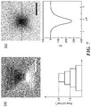
- FIG. 7 demonstrates three dimensional structure of silk resist: (a) SEM image (top) and the distribution of dose (bottom); (b) AFM image of the pattern (top) and the cross section profile (bottom).
- FIG. 8 provides comparison of silk resist with PMMA. SEM and AFM image of the square lattice pattern on the PMMA film (a, b) and the silk film (c, d). All scale bar represent 400 nm.
- FIG. 9 presents theoretical estimation of the gain enhancement.
- Photonic band-structure calculated by the PWE method At the band-edges (in red circle), the generated photons can be enhanced due to slow group velocity.
- the description of the super-cells used in the calculation is shown (right).
- the periodic slab is a reason that modes irrelevant to the 2D PhC are shown in the band-structure.
- FIG. 10 illustrates a representative embodiment of silk resist resolution.
- FIG. 11 provides images of nano-patterned voids produced on a silk film; Thickness of silk film ⁇ 160 nm, minimum feature size ⁇ 40 nm.
- FIG. 12 provides images of nano-patterned voids produced on a silk film; Thickness of silk film ⁇ 80 nm, minimum feature size ⁇ 40 nm.
- FIG. 13 provides images of nano-patterned voids produced on a silk film; Thickness of silk film ⁇ 80 nm, diameter of holes in CAD ⁇ 30 nm, and diameter of holes in SEM ⁇ 32 nm.
- FIG. 14 provides images of nano-patterned voids produced on a silk film: (a) 20 nm feature but uneven pattern; (b) 50 nm feature and diameters of ⁇ 50 nm and ⁇ 57 nm in SEM.
- FIG. 15 provides images of nano-patterned voids produced on a silk film having the thickness of ⁇ 160 nm: (a) ⁇ 30 nm feature, 35 nm and 33 nm in SEM; (b) ⁇ 20 nm feature, 25 nm in SEM.
- FIG. 16 provides an image of nano-patterned voids produced on a silk film; ⁇ 100 nm feature, 98 nm in SEM.
- Silk fibroin including the natural protein extracted from the Bombyx mori caterpillar, has been shown to be an attractive material for applications in bio-electronics and photonics due to its biocompatibility and unique mechanical and optical characteristics. 4, 5
- the favorable characteristics of silk fibroin films afford the adaptation of micro- and nano-fabrication techniques commonly used in organic electronics and photonics manufacturing.
- Silk fibroin-based materials embody the interface between technology and biology by complementing their material traits with the ability to be a biologically favorable carrier, in which bio-dopants such as biologics and other biologically active agents and therapeutics maintain their function. 7
- Silk-based nanoimprinting has been described. Water-based silk solution extracted from natural silk fibers can be used as a precursor that can be cast on various micro- and nano-structured molds, faithfully replicating their topographies. 8, 9 Nanoimprinting has been used to fabricate two dimensional photonic crystal (PhC) with feature sizes under 50 nm. 10 Additionally, microscale metal-patterns were successfully transferred to silk films and used as an etching mask or as conformal electrodes. 11, 12 However, most micro- and nano-fabrication techniques for generating desired patterns in silk fibroin-based materials or other polymers demand non-trivial fabrication steps involving the use of toxic chemicals or limit freedom of the pattern's diversity.
- EBL ultrahigh resolution electron-beam lithography
- PMMA poly(methyl methacrylate)
- the present invention combines the advantageous features of EBL and unique material properties of silk fibroin in realizing truly green nanopatterning.
- silk fibroin-based green lithography methods described herein are based on selective “ON-OFF” control of silk fibroin materials, conferred by differential solubility of the materials to water.
- the silk material is immobilized (e.g., annealed, crosslinked, etc.)
- the silk material is water-insoluble. Portions of silk fibroin material that are not immobilized can be washed away.
- the crystallinity of silk fibroin can be controlled at the nano-scale to provide either “soluble” or “insoluble” form of silk fibroin materials.
- silk resist e.g., silk fibroin materials
- Such silk resist can then be “developed” by a washing step so as to “wash away” or dissolve soluble portions of the silk resist. Insoluble or immobilized portions of silk resist remain intact.
- high-resolution, highly reproducible, inexpensive methods involving EBL can be carried out using an entirely water-based process.
- solubility refers to solubility of a material (such as silk fibroin-based materials) in an aqueous environment (e.g., using aqueous agents, such as water and water-based buffers), unless expressly stated otherwise.
- aqueous agents such as water and water-based buffers
- insoluble likewise refers to inability of a material to be soluble or be solubilized in an aqueous environment.
- an insoluble silk fibroin material is also characterized as “immobilized” in the context of the present disclosure.
- immobilization or “immobilizing” does not imply tethering to a support; rather, the term refers to structurally stabilized forms of silk fibroin that are not soluble in water or water-based buffers.
- immobilization occurs through molecular interactions of silk fibroin molecules.
- immobilization may involve intra- and/or inter-molecular interactions of fibroin molecules present in a silk fibroin material (or silk fibroin-based material). These interaction may comprise non-covalent interactions, such as hydrogen bonds, hydrophobic interactions, ionic interactions, as well as covalent bonds. In some embodiments, any of these interactions may take place in certain portions (or fragments) of silk fibroin molecule. In some embodiments, primarily hydrophobic stretches of the silk fibroin polypeptide mediate hydrophobic interactions, hydrogen bond formations, or both.
- the first mechanism is to induce annealing of silk fibroin; the second mechanism is to crosslink (or cross-link) silk fibroin.
- the first mechanism is to induce annealing of silk fibroin; the second mechanism is to crosslink (or cross-link) silk fibroin.
- the process of annealing involves increased non-covalent interactions of silk fibroin molecules to induce the formation of beta sheet secondary structures.
- Such non-covalent interactions may include intra-molecular interactions, inter-molecular interactions, or both.
- non-covalent interactions are mediated by hydrogen bonds, as well as hydrophobic interactions of silk fibroin molecules, which are associated with increased beta sheet formation.
- silk fibroin Upon reaching a certain critical level of beta sheet content, silk fibroin is rendered insoluble in an aqueous condition. This phenomenon is generally associated with greater crystallinity, and the status of such silk fibroin is referred to as the Silk II structure.
- “annealing” involves non-covalent interactions (e.g., the hydrogen bonds, hydrophobic interactions, etc.), which favor structural shift of silk fibroin into higher beta sheet content, such that silk fibroin is crystalized and thus made insoluble.
- organic solvent(s) such as alcohols, e.g., methanol, ethanol, isopropyl, acetone, etc.
- Such solvents have an effect of dehydrating silk fibroin, which promotes “packing” of silk fibroin molecules to favor the formation of beta sheet structures.
- plasticizing silk fibroin can be achieved by treating solidified but soluble forms of silk fibroin with a plasticizing agent.
- a plasticizing agent is water vapor. Water molecules of water vapor are thought to act as a plasticizer, which allows increased chain mobility of fibroin molecules to promote the formation of hydrogen bonds, leading to increased beta sheet secondary structures.
- a third novel means of annealing involves slow, controlled evaporation of water from silk fibroin.
- a silk fibroin solution or hydrolyzed silk fibroin material is allowed to evaporate at a low rate, often over hours or days.
- silk materials may be placed in a substantially closed chamber or container, in which the moisture content in the surrounding environment (e.g., humidity) is maintained relatively high. In this way, the rate of evaporation from the silk materials can be retarded.
- evaporation is allowed to occur at a humidity ranging between about 40% and 100%, e.g., about 40%, about 45%, about 50%, about 55%, about 60%, about 65%, about 70%, about 75%, about 80%, about 85%, about 90%, about 95%, and about 100%. It is contemplated that slow evaporation of water molecules from a silk fibroin material allows slow, more orderly “packing” of fibroin molecules into beta sheet structure, as compared to silk fibroin that is allowed to evaporate more rapidly at the same temperature, which leads to a higher degree of disorganization in the resulting silk fibroin structures upon solidification. Orderly packing means greater crystallinity of silk fibroin.
- annealed silk fibroin exhibits high degrees of crystallinity such that it becomes water-insoluble.
- “high degrees of crystallinity” refers to beta sheet contents of between about 20% and about 80%, e.g., about 20%, about 25%, about 30%, about 35%, about 40%, about 45%, about 50%, about 55%, about 60%, about 65% and about 75%, or greater.
- crosslinking refers to the formation of covalent bonds involving silk fibroin molecules.
- Crosslinking can immobilize silk fibroin molecules such that crosslinked silk fibroin material is insoluble in water. Unlike the process of annealing, however, this mode of immobilization does not depend on the formation of beta sheet structures in silk fibroin. Rather, crosslinked silk fibroin molecules are “fixed in place” so-to-speak, via covalent bonds.
- the process of crosslinking involves the formation of free radicals.
- the process of crosslinking preferentially affects certain amino acid residues of silk fibroin polypeptides.
- the process of crosslinking preferentially affects tyrosine residues of silk fibroin polypeptides.
- the process of crosslinking involves tyrosyl radicals.
- crosslinking is induced in silk fibroin comprising extra tyrosine residues, as compared to the native (or wild type) silk fibroin polypeptide sequence.
- recombinantly produced silk fibroin is used for crosslinking.
- silk fibroin is enriched with hydrophobic fragments of the silk fibroin polypeptide.
- crosslinking comprises the use of at least one crosslinking agents, such as polymers and linkers. In some embodiments, such crosslinking agents form covalent bonds with silk fibroin molecules via reactive groups.
- the basic premise underlining the present invention is the ability to control the ON/OFF states of silk fibroin resists by manipulating its solubility.
- two modes of silk fibroin-based green lithography are described herein: (i) the negative tone; and, (ii) the positive tone.
- the former involves selective removal of portion of silk resist, while the latter involves selective formation of immobilized portion of on otherwise soluble silk resists.
- an immobilized silk fibroin material is used to selectively solubilize at least a portion of the material to create corresponding structures (e.g., voids) upon such a material.
- the process involves electron beam lithography using immobilized or insoluble silk fibroin as a starting material (such as silk fibroin layer or film) which acts as a resist. Electron beam can be used for precise control of exposure upon the silk resist. Electron beam causes the breakage of weak non-covalent bonds, such as hydrogen bonds, in silk fibroin molecules, rendering the exposed portion water-soluble. Following the electron beam exposure, the silk fibroin material can then be “developed” by a simple washing step. The exposed portion is now dissolved and washed away, while leaving the unexposed portions of the silk fibroin materials intact. Because electron beam allows a nano-scale control, nanostructures may be fabricated on silk fibroin resist at high resolutions.
- a silk fibroin material is provided which is solidified but water-soluble form of silk fibroin material.
- such silk fibroin materials may be a silk fibroin film which has not been annealed, thus substantially water-soluble.
- At least a portion of such solidified silk fibroin material can be selectively immobilized in a predetermined spatial pattern by any suitable means.
- the resulting “chimeric” silk fibroin material comprises at least a portion where silk fibroin is immobilized at the molecular level, and at least a portion where silk fibroin is not immobilized at the molecular level.
- selective immobilization of the predetermined portion of silk fibroin material is carried out by the use of a high energy source, including but are not limited to irradiation, electron beam, etc.
- a high energy source including but are not limited to irradiation, electron beam, etc.
- crosslinking of silk fibroin is induced by exposing silk fibroin materials to electron beam.
- crosslinking of silk fibroin is induced by irradiation.
- crosslinking of silk fibroin comprises photo-crosslinking.
- crosslinking of silk fibroin comprises exposing silk fibroin materials to UV (e.g., UV crosslinking)
- crosslinking of silk fibroin is achieved by the use of at least one type of chemical linker.
- nanostructures may be fabricated, having a range of sizes, dimensions, shapes, patterns, and so on.
- nanostructures fabricated by any method described herein are substantially two-dimensional structures. “Substantially two-dimensional” means that the depth (e.g., height) of the structure is insignificant such that the structure is predominantly planer, which can be defined by its x-y configuration (area) of the structure. “Substantially three-dimensional” means that the depth (or height) of the structure is a meaningful feature, and such a structure may be defined by its x-y-z configuration (volume) of the structure.
- such a structure constitute a substantially cylindrical void or hole.
- the depth dimension of a 3D structure is varied.
- a series of EBL processes is performed to fabricate such a 3D structure having a “layered” effect.
- such structure is pyramidal.
- nanostructures fabricated by any method described herein comprise a plurality of nanostructures to form a pattern. In some embodiments, a plurality of nanostructures forms a periodic pattern. In some embodiments, a plurality of nanostructures forms an aperiodic pattern.
- nanostructures fabricated by any method described herein comprise photonic crystal.
- nanostructures of photonic crystal comprise a plurality of substantially cylindrical voids aligned in a pattern or patterns.
- diameters, depth, and/or distribution of such voids may be varied in a predetermined pattern to create structural colors.
- distances between adjacent voids e.g., spacing
- diameters of such voids can be varied.
- the distance between features may be measured “center-to-center” but in some embodiments the distance between features may be measured from the edge of one feature to the edge of an adjacent feature.
- the patent of the features may be rectangular, triangular or circular array, or any other suitable pattern.
- nanostructures fabricated by any method described herein are present at least on one surface.
- nanostructures are fabricated on a silk fibroin material in a form of a layer.
- silk fibroin layer can have a variety of dimensions and features.
- Such silk fibroin layers contemplated in some embodiments include those adhered to a substrate as well as those independent (e.g., either removed from) a substrate, in addition to free-standing silk fibroin materials.
- the thickness of the silk fibroin layer is typically determined by the coating methods and parameters of the silk fibroin solution. For example, high speed spin coating leads to thinner layers, while lower speed spin coating can lead to thicker layers.
- the thickness of the silk fibroin layer can be between about 40 nm and about 1000 nm, e.g., about 40 nm, about 50 nm, about 60 nm, about 70 nm, about 80 nm, about 90 nm, about 100 nm, about 150 nm, about 200 nm, about 250 nm, about 300 nm, about 350 nm, about 400 nm, about 450 nm, about 500 nm, and so on.
- the thickness may be between about 50 and about 100 nm, between about 50 nm and about 150 nm, between about 50 nm and about 200 nm, between about 50 nm and about 250 nm, between about 50 nm and about 300 nm, between about 50 nm and about 400 nm, between about 50 nm and about 500 nm, between about 100 nm and about 200 nm, between about 100 nm and about 250 nm, between about 100 nm and about 300 nm, between about 100 nm and about 400 nm, between about 100 nm and about 500 nm, between about 200 nm and about 250 nm, between about 200 nm and about 300 nm, between about 200 nm and about 400 nm, between about 200 nm and about 500 nm, between about 250 nm and about 300 nm, between about 250 nm and about 350 nm, between about 250 nm and about 400 nm, between about 250 nm
- a silk fibroin solution at a concentration lower than about 4%, more preferably lower than about 3%, lower than about 2.5%, lower than about 2%, lower than about 1.5%, lower than about 1%, e.g., about 0.9%, about 0.8%, about 0.7%, about 0.6%, about 0.5%.
- the silk fibroin nanostructures produced according to any of the methods in this disclosure include a variety of patterned features.
- the features may be a series of holes with diameters ranging from about 20 nm to about 200 nm.
- the diameter may be between about 20 nm and about 30 nm, between about 20 nm and about 50 nm, between about 20 nm and about 100 nm, between about 30 nm and about 100 nm, between about 30 nm and about 200 nm, between about 50 nm and about 100 nm, between about 50 nm and about 200 nm or, between about 100 nm and about 200 nm.
- the diameter is expressed as a ratio or proportion of the distance between features in a pattern (e.g., the lattice constant, ⁇ ,). In some embodiments, the diameter is between about 0.1 ⁇ and about 0.5 ⁇ (e.g, one tenth or one half of the distance between features, respectively).
- the features may commonly be described as holes, they have any varying depth, from a few nanometers from the surface of the silk biopolymer layer to penetrating through the entire thickness of silk fibroin layer.
- the cross-sectional shape of a feature though commonly described as a hole, implying a circular or elliptical cross-sectional shape, the features may instead by any cross-sectional shape (e.g., rectangular, hexagonal, elongated, or line).
- the cross-sectional shape of a feature may vary with depth depending on the application or process parameters in patterning. In instances in which the cross-section shape of a feature is not circular, the diameters described above may related to a primary dimension of the feature (e.g. major/minor axis, diagonal, width, etc.,).
- the patterns formed can vary. Though generally arrays of features, the patterns can ordered or random. In some embodiments, the ordered arrays can be rectangular, square, triangular or circular, depending on the use of the patterned silk product.
- the features may be spaced apparent from each other at regular intervals.
- the spacing between features may vary from between about 50 nm to about 1000 nm (i.e. 1 ⁇ m).
- the distance between features may be between about 50 nm and about 100 nm, between about 50 nm and about 300 nm, between about 50 nm and about 500 nm, between about 100 nm and about 200 nm, between about 100 nm and about 500 nm, between about 200 nm and about 300 nm, between about 200 nm and about 500 nm, between about 200 nm and about 1000 nm, between about 300 nm and about 500 nm, between about 300 nm and about 1000 nm, between about 500 nm and about 1000 nm.
- the distance between features is referred to as the lattice constant and given the symbol ⁇ .
- the diameters and distance between holes/voids of a nanopattern are key determinant factors to colors to be generated. See for example, PCT/US2012/068046, which is incorporated herein by reference in its entirety.
- Silk fibroin useful for carrying out the present invention includes a wide variety of silk fibroin polypeptide, fragments thereof, including preparations extracted from native sources, produced recombinantly, or chemically synthesized.
- Fibroin is a type of structural protein produced by certain spider and insect species that produce silk.
- Silk fibers such as those produced by silkworms or spiders, can be processed into silk fibroin which can then be processed into various forms including silk solutions (Jin & Kaplan, 424 Nature 1057 (2003)), gels (Jim et al., 5 Biomacromol. 786 (2004)), foams (Nazarov et al., 5 Biomacromol. 718 (2004)), and films (Jin et al., 15 Adv. Functional Mats. 1241 (2005); Amsden et al., 17 Optics Express 21271 (2009)).
- Various processing options enable its use as a supporting and packaging material for implanted micro and medical devices.
- silk fibroins matrices have outstanding biocompatibility, and excellent mechanical and optical properties, which make these materials well suited for a variety of implantable medical devices (IMDs). See, for example, Omenetto & Kaplan, 2 Nature Photonics 641 (2008). Additionally, silk films can be patterned (in both 2D and 3D) to realize a number of optical elements such as diffractive gratings (Amsden et al., 22 Adv. Mats. 1746 (2010)), and wave guides (Parker et al., 21 Adv. Mats. (2009)), within the IMDs. Silk fibroins also provide a biologically favorable microenvironment that allow to entrainment of various biological and/or chemical dopants and maintain their functionality.
- IMDs implantable medical devices
- Proteins (Bini et al., 335 J. Mol. Bio. 27 (2004)), enzymes (Lu et al., 10 Macromol. Biosci. 359 (2010)) and small organics (Lawrence et al., 9 Biomacromol. 1214 (2008)), have been incorporated into silk films for various biochemical functionalities.
- silk fibroin can be prepared in an all-aqueous process, further expanding its compatibility with biologics, manufacturing processes and the environment.
- silk fibroin includes silkworm fibroin and insect or spider silk protein. See e.g., Lucas et al., 13 Adv. Protein Chem. 107 (1958).
- silk fibroin useful for the present invention may be that produced by a number of species, including, without limitation: Antheraea mylitta; Antheraea pernyi; Antheraea yamamai; Galleria mellonella; Bombyx mori; Bombyx mandarins; Galleria mellonella; Nephila clavipes; Nephila senegalensis; Gasteracantha mammosa; Argiope aurantia; Araneus diadematus; Latrodectus geometricus; Araneus bicentenarius; Tetragnatha versicolor; Araneus ventricosus; Dolomedes tenebrosus; Euagrus chisoseus; Plectreu
- silk fibroin for use in accordance with the present invention may be produced by any such organism, or may be prepared through an artificial process, for example, involving genetic engineering of cells or organisms to produce a silk protein and/or chemical synthesis.
- silk is produced by the silkworm, Bombyx mori.
- silks are modular in design, with large internal repeats flanked by shorter ( ⁇ 100 amino acid) terminal domains (N and C termini).
- Silks have high molecular weight (200 to 350 kDa or higher) with transcripts of 10,000 base pairs and higher and >3000 amino acids (reviewed in Omenetto and Kaplan (2010) Science 329: 528-531).
- the larger modular domains are interrupted with relatively short spacers with hydrophobic charge groups in the case of silkworm silk.
- N- and C-termini are involved in the assembly and processing of silks, including pH control of assembly. The N- and C-termini are highly conserved, in spite of their relatively small size compared with the internal modules.
- An exemplary list of silk-producing species and corresponding silk proteins may be found in International Patent Publication Number WO 2011/130335, the entire contents of which are incorporated herein by reference.
- Cocoon silk produced by the silkworm, Bombyx mori is of particular interest because it offers low-cost, bulk-scale production suitable for a number of commercial applications, such as textile.
- Silkworm cocoon silk contains two structural proteins, the fibroin heavy chain ( ⁇ 350 k Da) and the fibroin light chain ( ⁇ 25 k Da), which are associated with a family of nonstructural proteins termed sericin, which glue the fibroin brings together in forming the cocoon.
- the heavy and light chains of fibroin are linked by a disulfide bond at the C-terminus of the two subunits (Takei, F., Kikuchi, Y., Kikuchi, A., Mizuno, S. and Shimura, K. (1987) J.
- silk fibroin embraces silk fibroin protein, whether produced by silkworm, spider, or other insect, or otherwise generated (Lucas et al., Adv. Protein Chem., 13: 107-242 (1958)).
- silk fibroin is obtained from a solution containing a dissolved silkworm silk or spider silk.
- silkworm silk fibroins are obtained, from the cocoon of Bombyx mori .
- spider silk fibroins are obtained, for example, from Nephila clavipes .
- silk fibroins suitable for use in the invention are obtained from a solution containing a genetically engineered silk harvested from bacteria, yeast, mammalian cells, transgenic animals or transgenic plants. See, e.g., WO 97/08315 and U.S. Pat. No. 5,245,012, each of which is incorporated herein as reference in its entirety.
- a silk solution is used to fabricate compositions of the present invention containing fibroin proteins, essentially free of sericins.
- silk solutions used to fabricate various compositions of the present invention contain the heavy chain of fibroin, but are essentially free of other proteins.
- silk solutions used to fabricate various compositions of the present invention contain both the heavy and light chains of fibroin, but are essentially free of other proteins.
- silk solutions used to fabricate various compositions of the present invention comprise both a heavy and a light chain of silk fibroin; in some such embodiments, the heavy chain and the light chain of silk fibroin are linked via at least one disulfide bond. In some embodiments where the heavy and light chains of fibroin are present, they are linked via one, two, three or more disulfide bonds.
- fibroin proteins share certain structural features.
- a general trend in silk fibroin structure is a sequence of amino acids that is characterized by usually alternating glycine and alanine, or alanine alone. Such configuration allows fibroin molecules to self-assemble into a beta-sheet conformation.
- These “Ala-rich” hydrophobic blocks are typically separated by segments of amino acids with bulky side-groups (e.g., hydrophilic spacers).
- a fibroin peptide contains multiple hydrophobic blocks, e.g., 3, 4, 5, 6, 7, 8, 9, 10, 11, 12, 13, 14, 15, 16, 17, 18, 19 and 20 hydrophobic blocks within the peptide. In some embodiments, a fibroin peptide contains between 4-17 hydrophobic blocks. In some embodiments of the invention, a fibroin peptide comprises at least one hydrophilic spacer sequence (“hydrophilic block”) that is about 4-50 amino acids in length.
- hydrophilic spacer sequences include: TGSSGFGPYVNGGYSG (SEQ ID NO: 14); YEYAWSSE (SEQ ID NO: 15); SDFGTGS (SEQ ID NO: 16); RRAGYDR (SEQ ID NO: 17); EVIVIDDR(SEQ ID NO: 18); TTIIEDLDITIDGADGPI (SEQ ID NO: 19) and TISEELTI (SEQ ID NO: 20).
- a fibroin peptide contains a hydrophilic spacer sequence that is a derivative of any one of the representative spacer sequences listed above. Such derivatives are at least 75%, at least 80%, at least 85%, at least 90%, or at least 95% identical to any one of the hydrophilic spacer sequences.
- a fibroin peptide suitable for the present invention contains no spacer.
- silks are fibrous proteins and are characterized by modular units linked together to form high molecular weight, highly repetitive proteins. These modular units or domains, each with specific amino acid sequences and chemistries, are thought to provide specific functions. For example, sequence motifs such as poly-alanine (polyA) and polyalanine-glycine (poly-AG) are inclined to be beta-sheet-forming; GXX motifs contribute to 31-helix formation; GXG motifs provide stiffness; and, GPGXX (SEQ ID NO: 22) contributes to beta-spiral formation. These are examples of key components in various silk structures whose positioning and arrangement are intimately tied with the end material properties of silk-based materials (reviewed in Omenetto and Kaplan (2010) Science 329: 528-531).
- the particular silk materials explicitly exemplified herein were typically prepared from material spun by silkworm, B. Mori .
- the complete sequence of the Bombyx mori fibroin gene has been determined (C.-Z Zhou, F Confalonieri, N Medina, Y Zivanovic, C Esnault and T Yang et al., Fine organization of Bombyx mori fibroin heavy chain gene, Nucl. Acids Res. 28 (2000), pp. 2413-2419).
- the fibroin coding sequence presents a spectacular organization, with a highly repetitive and G-rich ( ⁇ 45%) core flanked by non-repetitive 5′ and 3′ ends.
- This repetitive core is composed of alternate arrays of 12 repetitive and 11 amorphous domains.
- the sequences of the amorphous domains are evolutionarily conserved and the repetitive domains differ from each other in length by a variety of tandem repeats of subdomains of ⁇ 208 bp.
- the silkworm fibroin protein consists of layers of antiparallel beta sheets whose primary structure mainly consists of the recurrent amino acid sequence (Gly-Ser-Gly-Ala-Gly-Ala)n (SEQ ID NO: 21).
- the beta-sheet configuration of fibroin is largely responsible for the tensile strength of the material due to hydrogen bonds formed in these regions.
- fibroin is known to be highly elastic. Historically, these attributes have made it a material with applications in several areas, including textile manufacture.
- Fibroin is known to arrange itself in three structures at the macromolecular level, termed silk I, silk II, and silk III, the first two being the primary structures observed in nature.
- the silk II structure generally refers to the beta-sheet conformation of fibroin.
- Silk I which is the other main structure of silk fibroin, is a hydrated structure and is considered to be a necessary intermediate for the preorganization or prealignment of silk fibroin molecules.
- silk I structure is transformed into silk II structure after spinning process.
- silk I is the natural form of fibroin, as emitted from the Bombyx mori silk glands.
- Silk II refers to the arrangement of fibroin molecules in spun silk, which has greater strength and is often used commercially in various applications.
- the amino-acid sequence of the ⁇ -sheet forming crystalline region of fibroin is dominated by the hydrophobic sequence.
- Silk fibre formation involves shear and elongational stress acting on the fibroin solution (up to 30% wt/vol.) in the gland, causing fibroin in solution to crystallize.
- the process involves a lyotropic liquid crystal phase, which is transformed from a gel to a sol state during spinning—that is, a liquid crystal spinning process. Elongational flow orients the fibroin chains, and the liquid is converted into filaments.
- Silk III is a newly discovered structure of fibroin (Valluzzi, Regina; Gido, Samuel P.; Muller, Wayne; Kaplan, David L. (1999). “Orientation of silk III at the air-water interface”. International Journal of Biological Macromolecules 24: 237-242).
- Silk III is formed principally in solutions of fibroin at an interface (i.e. air-water interface, water-oil interface, etc.).
- Silk can assemble, and in fact can self-assemble, into crystalline structures.
- Silk fibroin can be fabricated into desired shapes and conformations, such as silk hydrogels (WO2005/012606; PCT/US08/65076), ultrathin films (WO2007/016524), thick films, conformal coatings (WO2005/000483; WO2005/123114), foams (WO 2005/012606), electrospun mats (WO 2004/000915), microspheres (PCT/US2007/020789), 3D porous matrices (WO2004/062697), solid blocks (WO2003/056297), microfluidic devices (PCT/US07/83646; PCT/US07/83634), electro-optical devices (PCT/US07/83639), and fibers with diameters ranging from the nanoscale (WO2004/000915) to several centimeters (U.S.
- silk fibroin can be processed into thin, mechanically robust films with excellent surface quality and optical transparency, which provides an ideal substrate acting as a mechanical support for high-technology materials, such as thin metal layers and contacts, semiconductor films, dielectric powders, nanoparticles, and the like.
- high-technology materials such as thin metal layers and contacts, semiconductor films, dielectric powders, nanoparticles, and the like.
- useful silk materials can be prepared through processes that can be carried out at room temperature and are water-based. Therefore, bio-molecules of interest can be readily incorporated into silk materials.
- silk fibroin produced by silkworms such as Bombyx mori
- silk fibroin may be attained by extracting sericin from the cocoons of B. mori .
- Organic silkworm cocoons are also commercially available.
- silks including spider silk (e.g., obtained from Nephila clavipes ), transgenic silks, genetically engineered silks, such as silks from bacteria, yeast, mammalian cells, transgenic animals, or transgenic plants (see, e.g., WO 97/08315; U.S.
- an aqueous silk fibroin solution may be prepared using techniques known in the art. Suitable processes for preparing silk fibroin solution are disclosed, for example, in U.S. patent application Ser. No. 11/247,358; WO/2005/012606; and WO/2008/127401.
- the silk aqueous solution can then be processed into silk matrix such as silk films, conformal coatings or layers, or 3-dimensional scaffolds, or electrospun fibers.
- a microfiltration step may be used herein.
- the prepared silk fibroin solution may be processed further by centrifugation and syringe based micro-filtration before further processing into silk matrix.
- silk fibroin-based electron beam lithography described herein may optionally employ a substrate, upon which a silk resist may be deposited. While not required, a substrate may provide a benefit of structural support, improved handling during manufacture and/or printing process, etc.
- a substrate may provide a benefit of structural support, improved handling during manufacture and/or printing process, etc.
- suitable substrates include, but are not limited to: paper, fabric, silicon, metal, organic and inorganic polymers, and so on.
- useful substrates may be rigid. In some embodiments, useful substrates may be malleable. In some embodiments, useful substrates may be flat. In some embodiments, useful substrates may be conforming. In some embodiments, a substrate itself comprises a silk fibroin material, e.g., a film, a block, a thread, a particle, a mesh, an object or an article.
- a silk fibroin material e.g., a film, a block, a thread, a particle, a mesh, an object or an article.
- Electron beam lithography is a form of maskless lithography which fabricates arbitrary patterns by a serial writing without the use of masks. Such process creates patterns in a serial manner that allows an ultrahigh-resolution patterning of arbitrary shapes with a minimum feature size as small as a few nanometers.
- EBL has been one of the main such techniques for fabricating nanoscale patterns.
- EBL helps overcome the limitation of light-based nanotechnology measuring and fabricating tools, which are dependent on the wavelength of light (as higher the wavelength of light, the higher the energy of the light, which could subsequently cause unwanted side effects).
- EBL utilizes an accelerated electron beam focusing on an electron-sensitive resist to make an exposure.
- Electrons can induce the deposition of substances onto a surface (additive/negative), or etch away at the surface (subtractive/positive). Also, electrons can be used to etch a “mask” whose patterns can be later transferred onto a substance using other techniques.
- Lithography techniques when combined with other fabrication processes such as deposition and etching, can be used to produce a high-resolution topography, and the cycle may be repeated several times to form complex micro/nanoscale structures.
- Micro- and nano-lithography techniques that have been the mainstay of the semiconductor and integrated circuit (IC) industry have been used to create patterns with a feature size ranging from a few nanometers up to tens of millimeters.
- Micro- and nano-lithography techniques have also been played an important role in manufacturing of commercial microelectromechanical system (MEMS) devices as well as prototype fabrication in emerging nanoscale science and engineering. These applications can significantly improve quality of life in many ways from electronic gadgets to healthcare and medical devices, for example, MEMS accelerometers employed in automobiles and consumer electronic devices, digital micromirror devices (DMD) for display applications in projectors and televisions, nanoelectronics for denser and faster computing, nanomedicine for diagnosis and treatment of diseases including, cancers, heart disease and Alzheimer's disease, nanoelectromechanical systems for high-sensitivity and high resolution sensing and manipulating, and nanobiosensors for ultra-low concentration and single molecular detection.
- MEMS accelerometers employed in automobiles and consumer electronic devices
- DMD digital micromirror devices
- nanoelectronics for denser and faster computing
- nanomedicine for diagnosis and treatment of diseases including, cancers, heart disease and Alzheimer's disease
- nanoelectromechanical systems for high-sensitivity and high resolution sens
- the inventors of the present application sought a novel approach to high resolution nanopatterning techniques, which would do away with the use of toxic and/or biohazardous materials typically involved in conventional lithography, while preserving comparable resolution.
- the present invention thus provides silk-based e-beam lithography that's entirely green.
- silk fibroin materials such as silk fibroin films
- silk fibroin films are known to offer excellent mechanical and optical properties (>90% transmission in the visible spectrum) and are currently being explored for applications in bio-electronics, optics, and bio-photonics
- the present application demonstrates for the first time that silk fibroin materials can be effectively used as silk resist in lithography in truly green processing that requires no harsh toxic solvents.
- the present application thus provides methods for silk-based lithography, which support the adaptation of micro- and nano-lithographic fabrication techniques in organic electronics and optical characteristics, using silk fibroin materials as resist. Such methodology takes advantage of silk fibroin cross-linking as the on/off control for lithography.
- the environmentally benign, all-aqueous processing conditions and the chemistry of silk allow the silk fibroin materials to embody the interface between technology and biology by complementing their material traits with the ability to be a biologically favorable carrier in which dopants such as quantum dots, enzymes and proteins maintain their function.
- These films possess useful properties that allow interfacing with metals and thin-film semiconductor devices, and the opportunity to develop biocompatible hybrid silk devices. This was recently demonstrated by using silk-based electrodes to measure neural activity in-vivo.
- Water-based silk solution extracted from natural silk fibers can be used as a precursor, similar to polydimethylsiloxane (PDMS), that can be cast on various micro- and nano-structured molds to replicate their surface topographies.
- PDMS polydimethylsiloxane
- microscale metal-patterns transferred to silk fibroin films can be used as an etching mask.
- Device manufacturing with silk fibroin films could provide benefits from fabrication methods that simplify patterning techniques by avoiding prolonged times of sample preparation, elevated temperature or high vacuum, which, aside from providing more complexity, would also limit the use of biologically active species.
- photonic crystal patterns may be generated onto silk fibroin resist by direct electron beam lithography.
- Such nanostructures may be fabricated with an suitable dose of electron beam, such as about 3000 ⁇ C/cm 2 .
- Microscope image may be acquired by illuminating the photonic crystal patterns with a white light source.
- the lattice constant of nanostructures and the numerical aperture (N. A.) of the microscope objective lens determine the diffractive colors across the different letters.
- FIG. 2( a ) silk nanostructure generated in positive tone resist may be observed in dark field microscopic image and SEM images.
- Each letter in the image “Tufts” shown in FIG. 2 is composed of the photonic crystal with different lattice constants (500, 600, and 700 nm), thereby revealing different structural colors. Same types of images may also be generated in negative tone resist, as demonstrated in FIG. 2( b ) . All scale bars represent 1 ⁇ m.
- the PhC patterns can be fabricated by varying the beam dose.
- the exposed dose ranges from 1000 ⁇ C/cm 2 to 5000 ⁇ C/cm 2 in 1000 ⁇ C/cm 2 increments.
- the optimal dose value to fabricate the PhC patterns may be about 3000 ⁇ C/cm 2 , which is approximately three times higher than what is needed to fabricate comparable structures with PMMA.
- the present invention includes lithographic methods for creating patterned silk fibroin layers.
- a silk solution is coated on a substrate.
- Silk fibroin solution can be coated on a substrate (e.g., glass slide) by any number of coating methods.
- Exemplary liquid coating methods include but are not limited to spin coating, chemical solution deposition, spraying, dipping, etc.
- the conditions of the coating method typically determine the thickness of both the silk biopolymer solution and the eventual silk biopolymer layer.
- the solution is dried to provide a silk biopolymer layer.
- the thickness of the solution can vary between about 50 nm and about 500 nm.
- the concentration of the silk solution can also influence the preparation steps, the thickness and/or the surface properties (such as smoothness or texture) of the silk biopolymer layer.
- Useful concentrations of silk fibroin typically range between about 0.4% and about 10%, e.g., 0.4%, 0.5%, 0.6%, 0.7%, 0.8%, 0.9%, 1%, 2%, 3%, 4%, 5%, 6%, 7%, 8%, 9%, 10%, 11%, 12%, 13%, 14%, 15%, 16%, 17%, 18%, 20%, 21%, 22%, 23%, 24% and 25%. It should be noted, however, that silk fibroin concentrations should be kept below 4% for spin coating methods. More preferably, silk fibroin concentrations should be kept below 3%, below 2%, below 1.5%, below 1%.
- the solution can dried to produce silk biopolymer layer.
- silk fibroin may be immobilized prior to drying, or after drying.
- the drying step may utilize any temperature and length of time need to produce a suitable silk fibroin layer.
- dehydrating gases can be used to create the silk biopolymer layer, as described in WO2007-016524.
- Annealing may also (e.g., formation of crystallized silk, formation of ⁇ -sheets) be induced in several different ways.
- exposure of silk fibroin materials to water vapor or alcohols (liquid or vapor) can induce beta sheet formation in the silk fibroin.
- the operating conditions involved in producing immobilized silk fibroin layer can vary depending on the method used. For example temperatures can range from about 4° C. temperature to about 200° C.
- the concentration of water (or alcohol) used to produce the annealed silk can vary from about 1% to about 100%.
- the portion of silk biopolymer layer immobilized can range from about all of (i.e., substantially all of) the silk biopolymer layer to a percentage less than about 1%.
- the end form of the silk biopolymer layer will determine the extent of the silk biopolymer layer that is immobilized. In some embodiments, the entire silk biopolymer layer is immobilized. In some embodiments, at least about 10%, at least about 20%, at least about 30%, at least about 40%, at least about 50%, at least about 60%, at least about 70%, at least about 80%, at least about 90% at least about 100% of the silk biopolymer layer is immobilized.
- the immobilized silk biopolymer layer can be patterned by exposure to energy sufficient to break the molecular bonds/interactions (e.g., hydrogen bonds) mediating annealing, e.g., between the silk fibroin molecules.
- this energy is supplied by electrons sourced from electron beam apparatuses described in more detail below. Energetic electrons can break weak chemical bonds such as hydrogen bonds in the crystallized silk film, so that the exposed area can become soluble and washed out by a solvent (e.g., water).
- FIG. 1 illustrates the general fabrication procedure of direct nano-pattering on silk film using EBL.
- other sources of electromagnetic radiation may supply the energy to break the molecular bonds/interactions so as to solubilize it.
- a silk biopolymer layer is prepared and then exposed to electromagnetic radiation (e.g., UV irradiation).
- electromagnetic radiation e.g., UV irradiation
- the silk biopolymer layer is not immobilized as part of the preparation.
- the electromagnetic radiation crosslinks the silk fibroin molecules.
- portions of the silk biopolymer layer exposed to the radiation will be crosslinked and becomes insoluble in a solvent, and un-exposed portions of the silk biopolymer layer will not be crosslinked and in turn will be soluble.
- the portions of the silk biopolymer layer exposed can be controlled to create a pattern in the silk biopolymer layer.
- the silk biopolymer layer After exposure to electromagnetic radiation, the silk biopolymer layer is developed by washing with a solvent, that removes the un-crosslinked silk biopolymer, leaving the crosslinked silk biopolymer. Again, the silk biopolymer layer can feature a patterned created by the electromagnetic radiation exposure.
- the “positive” (or subtractive) mode of electron beam lithography (often abbreviated as e-beam lithography, or EBL) is useful in creating nanostructures or an array thereof.
- EBL electron beam lithography
- the process of EBL involves emitting a beam of electrons in a patterned fashion across a surface covered with a film.
- the film or surface in some embodiments, is a silk biopolymer which is annealed.
- the silk biopolymer is coated on a substrate (e.g., by spin coating) in preparation of patterning.
- the electrons from the serve to break annealed bonds within the silk biopolymer layer, rendering the un-annealed portions soluble in a solvent (e.g., water).
- a solvent e.g., water
- any representative portion of the annealed silk biopolymer layer can have its non-covalent bonds broken by EBL.
- the portion of silk biopolymer layer that is no longer annealed after exposure to EBL can range from about all of the silk biopolymer layer to a percentage less than about 1%.
- the end form of the silk biopolymer layer will determine the extent of the silk biopolymer layer that is no longer annealed. In some embodiments, the entire silk biopolymer layer is no longer annealed. In some embodiments, at least about 10%, at least about 20%, at least about 30%, at least about 40%, at least about 50%, at least about 60%, at least about 70%, at least about 80%, at least about 90% at least about 100% of the silk biopolymer layer is no longer annealed.
- Electron beam lithography can operate under a variety of conditions which affect the structure of the final product, and the efficiency of the operation.
- the electron beam lithography system can vary the current, velocity of the electrons, the energetic dose applied to the substrate to be pattered (e.g., the silk biopolymer layer) as well as beam size, distance between the substrate and the focusing lens of the electron beam lithography device.
- the conditions of the electron beam are influenced by a variety of factors of the desired final product as well as the properties of the silk biopolymer layer being patterned.
- the diameter, spacing, lattice constant and thickness of the desired final product can determine the beam size, energy, duration and other operating parameters of the EBL process.
- the silk concentration, degree of immobilization of silk fibroin, thickness of the silk biopolymer layer will also influence the operation of the EBL process.
- the current used is on the order of nano-amperes (e.g. about 2 nA), but may vary from about 0.1 nA to about 100 nA. In some embodiments, the current is between about 0.1 nA and about 0.5 nA, between about 0.1 nA and about 1 nA, between about 0.1 nA and about 2 nA, between about 0.2 nA and about 1 nA, between about 0.1 nA and about 2 nA, between about 1 nA and about 5 nA, between about 1 nA and about 10 nA, between about 1 nA and about 20 nA, between about 5 nA and about 10 nA, between about 5 nA and about 20 nA, between about 5 nA and about 50 nA, between about 10 nA and about 20 nA, between about 10 nA and about 50 nA, between about 10 nA and about 100 nA, between about 20 nA and about 50 nA
- the energy dose varies between about 1000 ⁇ C/cm2 to about 5000 ⁇ C/cm2. In some embodiments, the energy dose is between about 1000 ⁇ C/cm2 and about 2000 ⁇ C/cm2, between about 1000 ⁇ C/cm2 and about 3000 ⁇ C/cm2, between about 1000 ⁇ C/cm2 and about 4000 ⁇ C/cm2, between about 2000 ⁇ C/cm2 and about 3000 ⁇ C/cm2, between about 2000 ⁇ C/cm2 and about 4000 ⁇ C/cm2, between about 2000 ⁇ C/cm2 and about 5000 ⁇ C/cm2, between about 3000 ⁇ C/cm2 and about 4000 ⁇ C/cm2, between about 3000 ⁇ C/cm2 and about 5000 ⁇ C/cm2 or between about 4000 ⁇ C/cm2 and about 5000 ⁇ C/cm2.
- the acceleration voltage can vary from about 10 keV to about 1000 keV. In some embodiments, the acceleration voltage is between about 10 keV to about 25 keV, between about 10 keV and about 50 keV, between about 10 keV and about 75 keV, between about 25 keV and about 50 keV, between about 25 keV and about 75 keV, between about 25 keV and about 100 keV, between about 50 keV and about 75 keV, between about 50 keV and about 100 keV, or between about 75 keV and about 100 keV.
- Suitable operating conditions of the electron beam lithography system can be selected and modified based on a wide variety of factors. These includes the thickness of the substrate to be pattered (e.g., the silk biopolymer layer), where thicker films may require higher doses. Additionally, the size and nature of the features to be patterned influences the operating conditions of the electron beam lithography. For examples, electron scattering and generation of secondary electrons within the substrate to be patterned are factors suggesting lower doses when features in the low range of diameters or distances between are sought.
- aqueous silk solution (concentration of about 1%) may be spin-coated on a glass substrate to form a thin silk film.
- the thickness can be controlled by spin-speed and concentration of silk solution (described herein).
- the water soluble film may be treated either by methanol (and the like) or water vapor to crystallize the silk protein. In both cases, these films can be expected to demonstrate similar resolution and quality of patterning.
- the electron beam patterning on the crystallized silk films may be carried out by using an EBL facility with 100 keV acceleration voltages. After exposure, the sample may be developed by immersion in distilled water to remove the exposed areas. All these fabrication steps may be carried out under all aqueous processing conditions.
- the silk biopolymer layer After patterning (e.g., creation of a pattern by EBL or by cross-linking), the silk biopolymer layer has portions that are no longer immobilized and other portions of soluble silk biopolymer.
- the latter portion of the silk biopolymer can be dissolved in a solvent (e.g., water) while the former portion of silk biopolymer is not soluble in the same solvent.
- the silk biopolymer layer is then “developed” by washing silk biopolymer layer in the solvent, which dissolves the water-soluble portion of the silk biopolymer layer, leaving the immobilized portion intact.
- the silk biopolymer layer can feature a pattern created by the electron exposure.
- the solvent is a non-toxic solvent. Exemplary solvents include but are not limited to water, and water-based buffers.
- the present invention provides a completely water-based approach to nano-patterning ( FIG. 1 ). This process is accomplished by eliminating unnecessary fabrication steps involving toxic chemicals and instead utilizing only EBL and water for direct nano-patterning of the silk fibroin protein.
- additional features may be incorporated for functionalization, including biological functionalization.
- the ability to easily dope silk with either inorganic and/or organic dopants provides augmented utility by allowing innumerable combinations of functionalized photoresists to be generated.
- PhC structures further comprising a light-sensitive element can be fabricated, which exhibit enhanced light-responsive signaling, providing evidence for the operativity of the present invention.
- manufacture and operational processes are entirely water-based and can be performed under ambient environment, it provides ample flexibility as to biological applications.
- methods described herein can be effectively adapted to include dopants that are biological in nature, such as proteins, cells, and so on, which are prone to degradation and/or inactivation under a number of harsh chemical or environmental conditions.
- the present silk fibroin materials of the present invention may be embedded or coated with at least one biologically active agent, such as: organic materials such as red blood cells, horseradish peroxidase, phenolsulfonphthalein, nucleic acid, a dye, a cell, an antibody, enzymes, for example, peroxidase, lipase, amylose, organophosphate dehydrogenase, ligases, restriction endonucleases, ribonucleases, DNA polymerases, glucose oxidase, laccase, cells, viruses, proteins, peptides, small molecules (e.g., drugs, dyes, amino acids, vitamins, antioxidants), DNA, RNA, RNAi, lipids, nucleotides, aptamers, carbohydrates, chromophores, light emitting organic compounds such as luciferin, carotenes and light emitting inorganic compounds (such as chemical dyes), antibiotics, antifungals, antivirals, light harvesting compounds such as chlorophyll
- silk fibroin materials useful for the present invention may also be prepared and used in conjunction with (e.g., in combination with) one or more of other natural biopolymers including chitosan, collagen, gelatin, agarose, chitin, polyhydroxyalkanoates, pullan, starch (amylose amylopectin), cellulose, hyaluronic acid, and related biopolymers.
- other natural biopolymers including chitosan, collagen, gelatin, agarose, chitin, polyhydroxyalkanoates, pullan, starch (amylose amylopectin), cellulose, hyaluronic acid, and related biopolymers.
- the present invention contemplates methods and compositions comprising two or more layers of silk fibroin materials (e.g., layers).
- Important advantages and functionality can be attained by the biopolymer photonic crystal in accordance with the present invention, whether it is implemented by a single film or by an assembly of stacked films.
- the biopolymer photonic structure can be biologically functionalized by optionally embedding it with one or more organic indicators, living cells, organisms, markers, proteins, and the like. It is therefore contemplated that each layer of a multi-layer silk fibroin composition (or similarly, each component of a multi-component silk fibroin composition) may be differentially or separately functionalized for desired effects.
- Electron beam lithography is still a ‘must-have’ and a ‘wide-use’ item to demonstrate nanostructures.
- Versatility and relatively long history of EBL make the method inviolable from other patterning techniques.
- Demonstrated herein are methods for carrying out all water-based direct electron beam patterning onto silk fibroin, a noble biological polymer. Without the requirement of toxic or volatile chemicals, but with the use of only water or water-based agents, unique chemical properties of silk fibroin make it possible to enable double-faced patterning (positive/negative tone).
- GFP green fluorescent protein
- PhC 2D photonic crystal
- the water-soluble silk fibroin and the sericin which is a water-soluble protein glue to coat the silk fiber, are spun together into a fiber, leading to a new insoluble conformation due to a rapid change in structure of the fibroin. 1,2
- the sericin is added to the surface of silk fibroin during spinning, and the result is the formation of the silk fiber.
- the silk fibroin solution can be extracted from the cocoon, a bunch of the silk fiber.
- a silk film coming from the silk solution has random coil complex, which is water soluble. These random coils can be modified to two structural forms by phase transition: silk I and silk II.
- Silk I refers to the complex helix-dominated structure existing within the caterpillars gland just before spinning, which is different from the water-soluble random-coil conformation of uncrystallized silk.
- Silk II is the water-insoluble antiparallel ⁇ -sheet crystal conformation, which forms after the spinning of silk fibers from the spinneret of the silkworm. Therefore the water-insoluble silk film can be achieved by increasing ⁇ -sheet content.
- the molecular structure in self-assembled silk fibroin films is basically random coil, which has water-soluble characteristics.
- the silk film can be made stable in water, such that silk fibroin is rendered water-insoluble.
- several techniques have been used to induce immobilization in silk fibroin material to make silk fibroin insoluble. The most common method is based on the chemical change during immersion of silk in organic solvents, such as methanol and ethanol. 16
- An alternative method, to maintain all water-based processing, is so-called “water vapor annealing” which uses water molecules to plasticize the system to promote a silk water-bound network with higher chain mobility. 17 More recently, a controlled, slow evaporation technique for inducing annealing in silk fibroin has been discovered.
- immobilization may also be carried out by a process herein referred to as crosslinking.
- crosslinking For example, high energy irradiant of ⁇ -ray or electron beam may be used to crosslink silk fibroin molecules. 18, 19
- Cross-linking methods are widely studied in polymer science in general but has not been well defined with respect to silk fibroin. Additionally high energy irradiation using g-ray and electron beam generates free-radicals, thereby cross-linking water-soluble polymers without requiring any added cross-linkers. 4 Recombination of the radicals results in the formation of covalent bonds and finally cross-linked structure.
- Poly(vinyl alcohol), poly(ethylene glycol), and poly(acrylic acid) are well-known examples of polymers which can be cross-linked with high energy irradiation. In biomolecules, silk would be an example for this technique.
- FIG. 1 illustrates the fabrication-procedure of direct nano-pattering on a silk film using EBL.
- Aqueous silk solution extracted from the Bombyx mori caterpillar was spin-coated on an arbitrary substrate such as a silicon and fused silica wafer to form a thin silk film. The thickness can be controlled by spin-speed and concentration of silk solution.
- the water soluble film was treated either by methanol or water vapor to induce annealing, in order to immobilize the silk protein.
- Immobilized silk fibroin films prepared by either one of the methods of annealing reveal similar resolution and the quality of the patterns.
- the electron beam patterning on the immobilized (positive resist) and non-immobilized (negative resist) silk films were carried out by using an EBL facility with 100 keV acceleration voltages. Energetic electrons can break weak chemical bonds, such as hydrogen bonds in the crystallized silk positive resist (or crosslink the silk proteins in the negative resist), so that the exposed area can become soluble and washed out by water (insoluble and stable in water). After exposure, the sample was “developed” by immersion in distilled water. It is worth noting that all these fabrication steps were carried out under all aqueous processing conditions.
- FIG. 2 shows the PhC patterns in the 200-nm-thick silk fibroin resist generated by the described method.
- the dark-field microscopic image was acquired by illuminating the photonic crystal patterns with a white light source.
- the lattice constant of the individual letters and the numerical aperture (N. A.) of the microscope objective lens determine the diffractive colors across the different letters.
- Scanning electron microscope (SEM) images reveals that high quality holes with the radii of 0.25 ⁇ were successfully generated in silk fibroin films. The quality of these nanostructures is comparable to patterns fabricated with commercial resists such as PMMA (see FIG. 8 ).
- FIG. 5 shows scanning electron microscope (SEM) images of the silk resist patterns with positive and negative tone.
- SEM scanning electron microscope
- FIGS. 6 ( a ) and ( b ) The sensitivity characteristics for silk resist are shown in FIGS. 6 ( a ) and ( b ) . Electron beam is exposed onto 5- ⁇ m-square area in the crystallized and amorphous silk film (270-nm-thickness) with different doses. After developing the film, the atomic force microscope (AFM) was used to obtain the depth (height) of the etched (remaining) patterns. Since surface profile of the pattern is not even, the depth and height are averaged.
- AFM atomic force microscope
- the threshold of sensitivity is about 2.25 mC/cm 2 (positive) and 25 mC/cm 2 (negative). These threshold values indicate that silk resist requires 11 times higher dose for the negative pattern than the positive pattern.
- the AFM images of the negative-tone patterns in which doses are between 25 and 80 mC/cm 2 show bumpy top-surfaces. At dose of over 90 mC/cm 2 , the surfaces become flatter ( FIG. 6( c ) ). We presume these values of dose aren't enough to build up perfect immobilization between silk molecules inside the block exposed by electron.
- the optimal dose value For a fixed beam current (2 nA) and high acceleration voltage (100 keV), we found the optimal dose value to be 2.25 mC/cm 2 (positive) and 25 mC/cm 2 (negative), which is approximately two times higher than what is needed to fabricate comparable structures with PMMA. 20, 21
- FIG. 7 shows SEM and AFM image of an inversed pyramid. Each pyramid was exposed 4 times with different dose and size. This technique is expected to be a building block for new types of subwavelength bio-photonic structures and nano-electronic components.
- the profile of silk resist is compared with poly(methyl methacrylate) (PMMA), most well-known and widely-used.
- PMMA poly(methyl methacrylate)
- the square-lattice pattern with 200-nm pitch size and 100-nm diameter was generated on the PMMA (130-nm-thick) and the silk (80-nm-thick) resist film.
- the dose value was 1 mC/cm 2 (PMMA) and 3 mC/cm 2 (silk).
- the radius of holes in the PMMA film is slightly larger than silk due to the proximity effect, silk can stand comparison with PMMA in the regards of the shape of holes and the cross section profile ( FIG. 8 ).
- the photons in the photonic crystal can propagate through the medium with extremely slow group velocity at the photonic band-edge, the point with zero slopes in the photonic band-structure. 5
- the PhC contains quantum elements, such as metal nanoparticle, quantum dot, and dye molecules, it provides a strong way to enhance their emission or absorption characteristics at the photonic band-edge.
- fluorescent enhancement with a fully biological protein-material system composed of silk fibroin and the super folder GFP (sfGFP) variant.
- the fluorescent protein dopant is ideal for biosensor applications due to high quantum yield, high extinction coefficient, and the high resistance against denaturing through solvent, pH, high temperature or photo bleaching.
- triangular PhC patterns with lattice constants ( ⁇ ) ranging from 300 to 600 nm with 50 nm increments are generated in which.
- the radius of hole is 0.3 ⁇ and the thickness of the silk film is 150 nm.
- the sample was excited from top surface using a 475 nm laser diode and the fluorescent emission was collected by an objective lens. The excitation light was blocked using a 495 nm long pass filter.
- FIG. 9 shows the calculated band-structure. Since the calculation assumed that the structure was periodically arranged in all three dimensional direction, many unnecessary modes (periodic slab modes) were shown in the band-structure. These modes could be filtered out by multiple calculations changing the dimension of the super-cell with normal direction to the slab. At around the normalized frequency of 0.8, there are several band-edge modes at F-point that can enhance the gain of GFP. For the sake of convenient comparison, the normalized frequencies were converted to the wavelength scale considering the lattice constant in FIG. 4 . Consistent with the experimental works in FIG. 3 , the emission of GFP was strongly enhanced at the band-edge location in the photonic structure.
- the normalized frequencies were converted to the wavelength-scale considering the lattice constant of the patterns.
- the band-edge modes that overlap the emission bandwidth of the GFP can be related to the enhanced extraction phenomena.
- deeper holes would increase the coupling efficiency between photons and the PhC structure, thereby improving the extraction efficiency.
- the high aspect ratio holes and therefore improved fluorescence extraction efficiency achieved with this direct EBL method improve on structures previously fabricated with nano imprinting methods.
- direct EBL of silk fibroin films proposes a relatively simple, green scheme.
- silk fibroin films can be used as a bio-based resist for direct electron-beam lithography.
- the process is entirely water based and offers a relatively simple method to generate nanoscale patterns with a high aspect ratio. in silk fibroin films.
- This approach eliminates the need to use chemicals, making this eco-friendly, and makes possible to achieve two-faced tone.
- Current studies i.e. multiple beam exposure and interference lithography
- the enhanced fluorescence emission from biologically derived GFP-doped silk PhC are the first steps to demonstrate the versatility of reformulating silk as a doped resist to add utility to materials that operate at the overlap of nanotechnology and biology.
- Cocoons of the Bombyx mori silkworm were boiled for 30 minutes in a solution of 0.02M Na 2 CO 3 to remove the sericin protein.
- the extracted fibroin was rinsed with distilled water and then dried in ambient air for 12 hours. After drying, the fibroin was dissolved in a 9.3M LiBr solution at 60° C. for 4 hours, yielding a 20 wt % aqueous solution, and subsequently the solution was dialyzed against distilled water using a dialysis cassette at room temperature for 48 hours until the solution reached a concentration of 8 wt %.
- the obtained solution was purified using a centrifuge and a 0.8 ⁇ m syringe filter.
- Fluorescent silk was prepared by adding fluorophores dissolved in water to the silk solution. The concentration of fluorescent silk solution was a 5.6 wt %.
- Silk fibroin solution was spin-coated on a silicon and fused silica substrate.
- 500 nm thick SiO 2 was deposited on the substrate using plasma enhanced chemical vapor deposition system prior to spin-coating.
- To crystallize the silk fibroin films the samples were treated in methanol at room temperature for one minute or water-vapor at 95° C. for two hours.
- An Elionix ELS-7000 system at 100 keV electron energy and 2 nA current was subsequently used.
- the exposed samples were developed in de-ionized water for a minute and dried using a nitrogen gas gun.
- the sfGFP plasmid vector was commercially obtained from Sandia BioTech/Theranostech, Inc. and transformed into chemically competent BL21 E. coli (Invitrogen) expression host. Transformed E. coli was plated on LB plates containing Kanamycin (Kan) (Fisher) antibiotic and incubated at 37° C. overnight. A single bacteria colony was selected and cultured at 37° C. overnight in 5 ml LB growth media (Fisher) containing Kan. The next day, a 2 liter volume LB growth media containing Kan was inoculated with the 5 ml starter culture and cultured shaking at 37° C.
- IPTG Isopropyl ⁇ -D-1-thiogalactopyranoside
- Wisher IPTG (Isopropyl ⁇ -D-1-thiogalactopyranoside) (Fisher) was added at OD 0.8 and cultured for an additional 5 h. Subsequently an E. coli pellet was obtained by centrifugation, re-suspended in lysis buffer and sonicated to aid cell lysis. sfGFP was purified by metal affinity column chromatography (NiNTA, Qiagen) and dialyzed. Aliquots were subsequently flash frozen and lyophilized until further use. For future use, sfGFP was re-suspended in DI water.
- Spectral-resolved microscopy of the fluorescence were performed using a multispectral CCD camera (CRI Nuance FX) connected to an Olympus IX 71 inverted microscope.
- the fluorescence was coupled to a 4 ⁇ objective lens with 0.17 N. A. and pumping light was blocked by a long pass filter with a cut wavelength of 495 nm for the GFP.
- the photonic band-structure which was calculated by a PWE method was achieved using the MPB software package distributed by MIT. Three dimensional calculations were performed.
- the refractive index was 1.54 (silk) and 1.45 (SiO 2 ).
- the thickness of the silk slab was 150 nm.
- the radius of holes was 0.3a (a is the lattice constant.) We have assumed that small amount of dopant does not significantly change the silk refractive index.
Abstract
Description
- 1 Tearney, G. J., Brezinski, M. E., Bouma, B. E., Boppart, S. A., Pitris, C., Southern J. F. & Fujimoto J. G. In vivo endoscopic optical biopsy with optical coherence tomography. Science 276, 2037-2039 (1997).
- 2 Chen, R. J., Bangsaruntip, S., Drouvalakis, K. A., Kam, N. W. S., Shim, M., Li, Y., Kim, W., Utz, P. J. & Dai, H. Noncovalent functionalization of carbon nanotubes for highly specific electronic biosensors.
PNAS 100, 4984-4989 (2003). - 3 Fan, X., White, I. M., Shopova, S. I., Zhu, H., Suter, J. D. & Sun, Y. Sensitive optical biosensors for unlabeled targets: A review Anal. Chim. Acta 620, 8-26 (2008).
- 4 Omenetto, F. G. & Kaplan, D. L. A new route for silk. Nature Photon. 2, 641-643 (2008).
- 5 Omenetto, F. G. & Kaplan, D. L. New opportunities for an ancient material. Science 329, 528-531 (2010).
- 6 Tao, H., Kaplan, D. L. & Omenetto, F. G. Silk materials—A road to sustainable high technology. Adv. Mater. 24, 2824-2837 (2012).
- 7 Pritchard, E. M., Dennis, P. B., Omenetto, F. G., Naik, R. R. & Kaplan, D. L. Physical and chemical aspects of stabilization of compounds in silk. Biopolymers 97, 479-498 (2012).
- 8 Perry, H., Gopinath, A., Kaplan, D. L., Negro, L. D. & Omenetto F. G. Nano- and micropatterning of optically transparent, mechanically robust, biocompatible silk fibroin films. Adv. Mater. 20, 3070-3072 (2008).
- 9 Kim, S., Mitropoulos, A. N., Spitzberg, J. D., Tao, H., Kaplan, D. L., & Omenetto, F. G. Silk inverse opals. Nature Photon. 6, 818-823 (2012).
- 10 Amsden, J. J., Domachuk, P., Gopinath, A., White, R. D., Negro, L. D., Kaplan, D. L. & Omenetto, F. G. Rapid nanoimprinting of silk fibroin films for biophotonic applications. Adv. Mater. 22, 1746-1749 (2010).
- 11 Tsioris, K., Tao, H., Liu, M., Hopwood, J. A., Kaplan, D. L., Averitt, R. D. & Omenetto, F. G. Adv. Mater. 23, 2015-2019 (2011).
- 12 Kim, D. H., Viventi, J., Amsden, J. J., Xiao, J., Vigeland, L., Kim, Y. S., Blanco, J. A., Panilatis, B., Frechette, E. S., Contreras, D., Kaplan, D. L., Omenetto, F. G., Huang, Y., Hwang, K. C., Zakin, M. R., Litt, B. & Rogers, J. A. Dissolvable films of silk fibroin for ultrathin conformal bio-integrated electronics. Nature Mater. 9, 511-517 (2010).
- 13 Martiradonna, L., Qualtieri, A., Stomeo, T., Carbone, L., Cingolani, R. & Vittorio, M. D. Lithographic nano-patterning of colloidal nanocrystal emitters for the fabrication of waveguide photonic devices. Sens. Act. B 126, 116-119 (2007).
- 14 Bae, M., Gemeinhart, R. A., Divan, R., Suthar, K. J. & Mancini, D. C. Fabrication of poly(ethylene glycol) hydrogel structures for pharmaceutical applications using electron beam and optical lithography. J. Vac. Sci. Technol. B 28, C6P24 (2010).
- 15 Jones, R. A., Li, W. X., Spaeth, H. & Steckl, A. J. Direct write electron beam patterning of DNA complex thin films. J. Vac. Sci. Technol. B 26, 2567 (2008).
- 16 Hu, X., Kaplan, D. L. & Cebe, P. Dynamic protein-water relationships during β-sheet formation. Macromolecules 41, 3939-3948 (2008).
- 17 Hu, X., Shmelev, K., Sun, L., Gil, E. S., Park, S. H., Cebe, P. & Kaplan, D. L. Regulation of silk material structure by temperature-controlled water vapor annealing.
Biomacromolucules 12, 1686-1696 (2011). - 18 Kojthung, A., Meesilpa, P., Sudatis, B., Treeratanapiboon, L., Udomsangpetch, R. & Oonkhanond, B. Effects of gamma radiation on biodegradation of Bombyx mori silk fibroin. Int. Biodeterioration & Biodegradation 62, 487-490 (2008).
- 19 Liu, J., Shao, J. & Zheng, J. Radiation grafting/crosslinking of silk using electron-beam irradiation. J. Appl. Poly. Sci. 91, 2028-2034 (2004).
- 20 Chen, W. & Ahmed, H. Fabrication of 5-7 nm wide etched lines in silicon using 100 keV electron-beam lithography and polymethylmethacrylate resist. Appl. Phys. Lett. 62, 1499-1501 (1993).
- 21 Duan, H., Winston, D., Yang, J. K. W., Cord, B. M., Manfrinato, V. R. & Berggren, K. K. Sub-10 nm half-pitch electron-beam lithography by using poly(methylmethacrylate) as a negative resist. J. Vac. Sci. Technol. B 28, 1071-1023 (2010).
- 22 Tarhan, I. I. & Watson, G. H. Photonic band structure of fcc colloidal crystals. Phys. Rev. Lett. 76, 315-318 (1996).
- 23 Kim, S., Lee, J., Jeon, H. & Kim. H. J. Fiber-coupled surface-emitting photonic crystal band edge laser for biochemical sensor applications. Appl. Phys. Lett. 94, 133503 (2009).
- 24 Tan, Y., Quan, W., Ding, S. & Wang, Y. Gold-nanoparticle-infiltrated polystyrene inverse opals: a three-dimensional platform for generating combined optical properties. Chem. Mater. 18, 3385-3389 (2006).
- 25 Pédelacq, J.-D., Cabantous, S., Tran, T., Terwillinger, T. C. & Waldo, G. S. Engineering and characterization of a superfolder green fluorescent protein. Nature Biotech. 24, 79-88 (2005).
- 26 Ferrini, R., Houdré, R., Benisty, H., Qiu, M. & Moosburger, J. Radiation losses in planar photonic crystals: two-dimensional representation of hole depth and shape by an imaginary dielectric constant. J. Opt. Soc.
Am. B 20, 469-478 (2003). - 27 Mondia J. P., Amsden, J. J., Lin, D., Negro, L. D., Kaplan, D. L. & Omenetto, F. G. Rapid nanoimprinting of doped silk films for enhanced fluorescent emission. Adv. Mater. 22, 4596-4599 (2010).
- 28 Multibeam Co. http://www.multibeamcorp.com
- 29 Solak, H. H., David, C., Gobrecht, J., Wang, L. & Cerrina, F. Multiple-beam interference lithography with electron beam written gratings. J. Vac. Sci. & Technol.
B 20, 2844-2848 (2002). - 30 Hu, X., Kaplan, D. L. & Cebe, P., Determining beta-sheet crystallinity in fibrous proteins by thermal analysis and infrared spectroscopy.
Macromolecules 39, 6161-6170 (2006). - 31 Jin, H.-J. & Kaplan, D. L. Mechanism of silk processing in insects and spiders. Nature 424, 1057-1061 (2003).
- 32 Hennink, W. E. & Nostrum, C. F. van Novel crosslinking methods to design hydrogels. Adv. Drug Del. Rev. 64, 223-236 (2012).
- 33 Dowling, J. P., Scalora, M., Bloemer, M. J. & Bowden, C. M. The photonic band edge laser: A new approach to gain enhancement. J. Appl. Phys. 75, 1896 (1994).
- 34 Johnson, S. G. & Joannopoulos, J. D. Block-iterative frequency-domain methods for Maxwell's equations in a planewave basis. Opt. Express 8, 173-190 (2001).
- Certain aspects of the present invention relate to the following patent applications, the contents of which are incorporated by reference herein: WO 2008/127404; WO 2008/118211; WO 2008/127402; WO 2008/127403; WO 2008/127401; WO 2008/140562; WO 2008/127405; WO 2009/061823; WO 2009/155397; WO 2010/126640; WO 2011/046652; WO 2011/026101; WO 2011/160098; WO 2012/054121; WO 2011/115643; WO 2011/130335; WO 2011/112931; WO 2012/047682; WO 2012/031282; WO 2012/094436; WO/2012/145739; PCT/US12/68046; PCT/US12/59834 and U.S. Provisional Application 61/791,358 (filed Mar. 15, 2013, entitled “SILK WATER LITHOGRAPHY.”
Claims (16)
Priority Applications (1)
| Application Number | Priority Date | Filing Date | Title |
|---|---|---|---|
| US14/776,083 US11009792B2 (en) | 2013-03-15 | 2014-03-14 | All water-based nanopatterning |
Applications Claiming Priority (3)
| Application Number | Priority Date | Filing Date | Title |
|---|---|---|---|
| US201361788520P | 2013-03-15 | 2013-03-15 | |
| US14/776,083 US11009792B2 (en) | 2013-03-15 | 2014-03-14 | All water-based nanopatterning |
| PCT/US2014/029571 WO2014197093A2 (en) | 2013-03-15 | 2014-03-14 | All water-based nanopatterning |
Publications (2)
| Publication Number | Publication Date |
|---|---|
| US20160033861A1 US20160033861A1 (en) | 2016-02-04 |
| US11009792B2 true US11009792B2 (en) | 2021-05-18 |
Family
ID=52008717
Family Applications (1)
| Application Number | Title | Priority Date | Filing Date |
|---|---|---|---|
| US14/776,083 Active US11009792B2 (en) | 2013-03-15 | 2014-03-14 | All water-based nanopatterning |
Country Status (2)
| Country | Link |
|---|---|
| US (1) | US11009792B2 (en) |
| WO (1) | WO2014197093A2 (en) |
Families Citing this family (8)
| Publication number | Priority date | Publication date | Assignee | Title |
|---|---|---|---|---|
| WO2014144971A1 (en) | 2013-03-15 | 2014-09-18 | Tufts University | Silk water lithography |
| WO2014197093A2 (en) | 2013-03-15 | 2014-12-11 | Tufts University | All water-based nanopatterning |
| US10944398B2 (en) * | 2016-09-30 | 2021-03-09 | Uchicago Argonne, Llc | Systems and methods for ultrafast plasmonic response in doped, colloidal nanostructures |
| US11331019B2 (en) | 2017-08-07 | 2022-05-17 | The Research Foundation For The State University Of New York | Nanoparticle sensor having a nanofibrous membrane scaffold |
| CN109553673B (en) * | 2017-09-25 | 2023-04-25 | 中国科学院上海微系统与信息技术研究所 | Biological protein building block and preparation method thereof |
| WO2019063590A1 (en) * | 2017-09-26 | 2019-04-04 | Spiber Technologies Ab | Structuring of surface-active macromolecules |
| CN109337892B (en) * | 2018-11-27 | 2021-11-19 | 贺州学院 | Method for immobilizing taro polyphenol oxidase by using fibroin |
| CN115960467A (en) * | 2023-01-20 | 2023-04-14 | 中国科学院苏州纳米技术与纳米仿生研究所 | Silk fibroin liquid crystal suspension and preparation method and application thereof |
Citations (41)
| Publication number | Priority date | Publication date | Assignee | Title |
|---|---|---|---|---|
| US5245012A (en) | 1990-04-19 | 1993-09-14 | The United States Of America As Represented By The Secretary Of The Army | Method to achieve solubilization of spider silk proteins |
| JPH07292306A (en) | 1994-04-22 | 1995-11-07 | Idemitsu Petrochem Co Ltd | Ink containing silk fibroin ultrafine powder |
| WO1997008315A1 (en) | 1995-08-22 | 1997-03-06 | Basel Richard M | Cloning methods for high strength spider silk proteins |
| JP2001152024A (en) * | 1999-11-24 | 2001-06-05 | Japan Atom Energy Res Inst | Method of micro pulverizing and water solubilizing silk fiber |
| WO2003056297A2 (en) | 2001-10-02 | 2003-07-10 | Trustees Of Tufts College | Self-assembling polymers, and materials fabricated therefrom |
| WO2004000915A2 (en) | 2002-06-24 | 2003-12-31 | Tufts University | Silk biomaterials and methods of use thereof |
| WO2004062697A2 (en) | 2003-01-07 | 2004-07-29 | Tufts University | Silk fibroin materials and use thereof |
| WO2005000483A1 (en) | 2003-06-06 | 2005-01-06 | Tufts University | Method for forming inorganic coatings |
| WO2005012606A2 (en) | 2003-04-10 | 2005-02-10 | Tufts University | Concentrated aqueous silk fibroin solution and use thereof |
| JP2005052162A (en) * | 2003-04-10 | 2005-03-03 | Silk Kogei:Kk | Production method of silk fibroin film |
| US6902932B2 (en) | 2001-11-16 | 2005-06-07 | Tissue Regeneration, Inc. | Helically organized silk fibroin fiber bundles for matrices in tissue engineering |
| WO2005123114A2 (en) | 2004-06-11 | 2005-12-29 | Trustees Of Tufts College | Silk-based drug delivery system |
| WO2007016524A2 (en) | 2005-08-02 | 2007-02-08 | Trustees Of Tufts College | Methods for stepwise deposition of silk fibroin coatings |
| WO2008118211A2 (en) | 2006-11-03 | 2008-10-02 | Trustees Of Tufts College | Biopolymer photonic crystals and method of manufacturing the same |
| WO2008118133A2 (en) | 2006-09-26 | 2008-10-02 | Trustees Of Tufts College | Silk microspheres for encapsulation and controlled release |
| WO2008127402A2 (en) | 2006-11-03 | 2008-10-23 | Trustees Of Tufts College | Biopolymer sensor and method of manufacturing the same |
| WO2008127403A2 (en) | 2006-11-03 | 2008-10-23 | Trustees Of Tufts College | Biopolymer optofluidic device and method of manufacturing the same |
| WO2008127405A2 (en) | 2006-11-03 | 2008-10-23 | Trustees Of Tufts College | Microfluidic device with a cylindrical microchannel and a method for fabricating same |
| WO2008127404A2 (en) | 2006-11-03 | 2008-10-23 | Trustees Of Tufts College | Nanopatterned biopolymer optical device and method of manufacturing the same |
| WO2008150861A1 (en) | 2007-05-29 | 2008-12-11 | Trustees Of Tufts College | Method for silk fibroin gelation using sonication |
| WO2009061823A1 (en) | 2007-11-05 | 2009-05-14 | Trustees Of Tufts College | Fabrication of silk fibroin photonic structures by nanocontact imprinting |
| WO2009155397A2 (en) | 2008-06-18 | 2009-12-23 | Trustees Of Tufts College | Edible holographic silk products |
| WO2010126640A2 (en) | 2009-02-12 | 2010-11-04 | Trustees Of Tufts College | Nanoimprinting of silk fibroin structures for biomedical and biophotonic applications |
| WO2011012931A1 (en) | 2009-07-31 | 2011-02-03 | Elsan Hammadde Sanayi Anonim Sirketi | Low lead brass alloy containing rare earth elements |
| WO2011026101A2 (en) | 2009-08-31 | 2011-03-03 | Trustees Of Tufts College | Silk transistor devices |
| WO2011046652A2 (en) | 2009-07-20 | 2011-04-21 | Trustees Of Tufts College | All-protein implantable, resorbable reflectors |
| WO2011115643A1 (en) | 2010-03-17 | 2011-09-22 | The Board Of Trustees Of The University Of Illinois | Implantable biomedical devices on bioresorbable substrates |
| WO2011130335A2 (en) | 2010-04-12 | 2011-10-20 | Tufts University | Silk electronic components |
| US20110293898A1 (en) | 2010-05-28 | 2011-12-01 | Seiko Epson Corporation | Ink set, textile printing method and printed textile |
| WO2011160098A2 (en) | 2010-06-17 | 2011-12-22 | Tufts University | Silk optical particles and uses thereof |
| WO2012031282A2 (en) | 2010-09-03 | 2012-03-08 | Tufts University/Trustees Of Tufts College | Plasmonic nanoparticle-doped silk materials |
| WO2012047682A2 (en) | 2010-09-27 | 2012-04-12 | Tufts University Trustees Of Tufts College | Silk-based piezoelectric materials |
| WO2012054121A2 (en) | 2010-07-30 | 2012-04-26 | Tufts University/Trustees Of Tufts College | Silk-based biophotonic sensors |
| WO2012094436A2 (en) | 2011-01-04 | 2012-07-12 | Tufts University/Trustees Of Tufts College | Electronic components on paper-based substrates |
| US20120268519A1 (en) | 2007-02-23 | 2012-10-25 | Konica Minolta Holdings, Inc. | Water-based ink jet ink and recording method |
| WO2012145739A1 (en) | 2011-04-21 | 2012-10-26 | Trustees Of Tufts College | Compositions and methods for stabilization of active agents |
| WO2013103424A2 (en) | 2011-10-11 | 2013-07-11 | Tufts University | Silk-based multifunctional biomedical platform |
| WO2013130156A2 (en) | 2011-12-05 | 2013-09-06 | Tufts University | Signal enhancement by silk photonic crystals |
| WO2014144971A1 (en) | 2013-03-15 | 2014-09-18 | Tufts University | Silk water lithography |
| WO2014197093A2 (en) | 2013-03-15 | 2014-12-11 | Tufts University | All water-based nanopatterning |
| US20150376248A1 (en) * | 2013-02-06 | 2015-12-31 | Virginia Commonwealth University | Photoactive silk protein and fabrication of silk protein structures using photolithography |
-
2014
- 2014-03-14 WO PCT/US2014/029571 patent/WO2014197093A2/en active Application Filing
- 2014-03-14 US US14/776,083 patent/US11009792B2/en active Active
Patent Citations (49)
| Publication number | Priority date | Publication date | Assignee | Title |
|---|---|---|---|---|
| US5245012A (en) | 1990-04-19 | 1993-09-14 | The United States Of America As Represented By The Secretary Of The Army | Method to achieve solubilization of spider silk proteins |
| JPH07292306A (en) | 1994-04-22 | 1995-11-07 | Idemitsu Petrochem Co Ltd | Ink containing silk fibroin ultrafine powder |
| WO1997008315A1 (en) | 1995-08-22 | 1997-03-06 | Basel Richard M | Cloning methods for high strength spider silk proteins |
| JP2001152024A (en) * | 1999-11-24 | 2001-06-05 | Japan Atom Energy Res Inst | Method of micro pulverizing and water solubilizing silk fiber |
| WO2003056297A2 (en) | 2001-10-02 | 2003-07-10 | Trustees Of Tufts College | Self-assembling polymers, and materials fabricated therefrom |
| US6902932B2 (en) | 2001-11-16 | 2005-06-07 | Tissue Regeneration, Inc. | Helically organized silk fibroin fiber bundles for matrices in tissue engineering |
| WO2004000915A2 (en) | 2002-06-24 | 2003-12-31 | Tufts University | Silk biomaterials and methods of use thereof |
| WO2004062697A2 (en) | 2003-01-07 | 2004-07-29 | Tufts University | Silk fibroin materials and use thereof |
| WO2005012606A2 (en) | 2003-04-10 | 2005-02-10 | Tufts University | Concentrated aqueous silk fibroin solution and use thereof |
| JP2005052162A (en) * | 2003-04-10 | 2005-03-03 | Silk Kogei:Kk | Production method of silk fibroin film |
| US7635755B2 (en) | 2003-04-10 | 2009-12-22 | Trustees Of Tufts College | Concentrated aqueous silk fibroin solution and use thereof |
| US20070187862A1 (en) | 2003-04-10 | 2007-08-16 | Trustees Of Tufts College | Concentrated aqueous silk fibroin solution and use thereof |
| WO2005000483A1 (en) | 2003-06-06 | 2005-01-06 | Tufts University | Method for forming inorganic coatings |
| WO2005123114A2 (en) | 2004-06-11 | 2005-12-29 | Trustees Of Tufts College | Silk-based drug delivery system |
| WO2007016524A2 (en) | 2005-08-02 | 2007-02-08 | Trustees Of Tufts College | Methods for stepwise deposition of silk fibroin coatings |
| WO2008118133A2 (en) | 2006-09-26 | 2008-10-02 | Trustees Of Tufts College | Silk microspheres for encapsulation and controlled release |
| US8195021B2 (en) | 2006-11-03 | 2012-06-05 | Tufts University/Trustees Of Tufts College | Biopolymer optical waveguide and method of manufacturing the same |
| WO2008127402A2 (en) | 2006-11-03 | 2008-10-23 | Trustees Of Tufts College | Biopolymer sensor and method of manufacturing the same |
| WO2008127403A2 (en) | 2006-11-03 | 2008-10-23 | Trustees Of Tufts College | Biopolymer optofluidic device and method of manufacturing the same |
| WO2008127405A2 (en) | 2006-11-03 | 2008-10-23 | Trustees Of Tufts College | Microfluidic device with a cylindrical microchannel and a method for fabricating same |
| WO2008127401A2 (en) | 2006-11-03 | 2008-10-23 | Trustees Of Tufts College | Biopolymer optical waveguide and method of manufacturing the same |
| WO2008127404A2 (en) | 2006-11-03 | 2008-10-23 | Trustees Of Tufts College | Nanopatterned biopolymer optical device and method of manufacturing the same |
| WO2008140562A2 (en) | 2006-11-03 | 2008-11-20 | Trustees Of Tufts College | Electroactive biopolymer optical and electro-optical devices and method of manufacturing the same |
| WO2008118211A2 (en) | 2006-11-03 | 2008-10-02 | Trustees Of Tufts College | Biopolymer photonic crystals and method of manufacturing the same |
| US20100070068A1 (en) | 2006-11-03 | 2010-03-18 | Trustees Of Tufts College | Biopolymer sensor and method of manufacturing the same |
| US20120268519A1 (en) | 2007-02-23 | 2012-10-25 | Konica Minolta Holdings, Inc. | Water-based ink jet ink and recording method |
| WO2008150861A1 (en) | 2007-05-29 | 2008-12-11 | Trustees Of Tufts College | Method for silk fibroin gelation using sonication |
| WO2009061823A1 (en) | 2007-11-05 | 2009-05-14 | Trustees Of Tufts College | Fabrication of silk fibroin photonic structures by nanocontact imprinting |
| US20120121820A1 (en) | 2007-11-05 | 2012-05-17 | Trustees Of Boston University | Fabrication of silk fibroin photonic structures by nanocontact imprinting |
| WO2009155397A2 (en) | 2008-06-18 | 2009-12-23 | Trustees Of Tufts College | Edible holographic silk products |
| WO2010126640A2 (en) | 2009-02-12 | 2010-11-04 | Trustees Of Tufts College | Nanoimprinting of silk fibroin structures for biomedical and biophotonic applications |
| WO2011046652A2 (en) | 2009-07-20 | 2011-04-21 | Trustees Of Tufts College | All-protein implantable, resorbable reflectors |
| WO2011012931A1 (en) | 2009-07-31 | 2011-02-03 | Elsan Hammadde Sanayi Anonim Sirketi | Low lead brass alloy containing rare earth elements |
| WO2011026101A2 (en) | 2009-08-31 | 2011-03-03 | Trustees Of Tufts College | Silk transistor devices |
| WO2011115643A1 (en) | 2010-03-17 | 2011-09-22 | The Board Of Trustees Of The University Of Illinois | Implantable biomedical devices on bioresorbable substrates |
| WO2011130335A2 (en) | 2010-04-12 | 2011-10-20 | Tufts University | Silk electronic components |
| US20110293898A1 (en) | 2010-05-28 | 2011-12-01 | Seiko Epson Corporation | Ink set, textile printing method and printed textile |
| WO2011160098A2 (en) | 2010-06-17 | 2011-12-22 | Tufts University | Silk optical particles and uses thereof |
| WO2012054121A2 (en) | 2010-07-30 | 2012-04-26 | Tufts University/Trustees Of Tufts College | Silk-based biophotonic sensors |
| WO2012031282A2 (en) | 2010-09-03 | 2012-03-08 | Tufts University/Trustees Of Tufts College | Plasmonic nanoparticle-doped silk materials |
| WO2012047682A2 (en) | 2010-09-27 | 2012-04-12 | Tufts University Trustees Of Tufts College | Silk-based piezoelectric materials |
| WO2012094436A2 (en) | 2011-01-04 | 2012-07-12 | Tufts University/Trustees Of Tufts College | Electronic components on paper-based substrates |
| WO2012145739A1 (en) | 2011-04-21 | 2012-10-26 | Trustees Of Tufts College | Compositions and methods for stabilization of active agents |
| WO2013103424A2 (en) | 2011-10-11 | 2013-07-11 | Tufts University | Silk-based multifunctional biomedical platform |
| WO2013130156A2 (en) | 2011-12-05 | 2013-09-06 | Tufts University | Signal enhancement by silk photonic crystals |
| US20150376248A1 (en) * | 2013-02-06 | 2015-12-31 | Virginia Commonwealth University | Photoactive silk protein and fabrication of silk protein structures using photolithography |
| WO2014144971A1 (en) | 2013-03-15 | 2014-09-18 | Tufts University | Silk water lithography |
| WO2014197093A2 (en) | 2013-03-15 | 2014-12-11 | Tufts University | All water-based nanopatterning |
| US20160046138A1 (en) | 2013-03-15 | 2016-02-18 | Tufts University | Silk water lithography |
Non-Patent Citations (56)
| Title |
|---|
| Amsden et al., Spectral analysis of induced color change on periodically nanopatterned silk films, Optics Express 17(23): 21271-21279 (2009). |
| Amsden, J.J. et al., Rapid Nanoimprinting of Silk Fibroin Films for Biophotonic Applications, Advanced Materials, 22(15):1746-1749 (2010). |
| Bae et al., Fabrication of Poly(ethylene glycol) Hydrogel Structures for Pharmaceutical Applications using Electron beam and Optical Lithography, J. Vac. Sci., Technol. 28(6); C6P24-C6P29 (2010). |
| Bini et al., Mapping Domain Structures in Silks from Insects and Spiders Related to Protein Assembly, J. Mol. Biol. 335: 27-40 (2004). |
| Brenckle, M.A. et al., Protein-protein nanoimprinting of silk fibroin films, Advanced Materials, 25:(17) 2409-2414 (2013). |
| Chen et al., Noncovalent functionalization of carbon nanotubes for highly specific electronic biosensors., PNAS 100(9): 4984-4989 (2003). |
| Chen, W. & Ahmed H. Fabrication of 5-7 nm wide etched lines in silicon using 100 ke V electron-beam lithography and polymethylmethacrylate resist. Appl. Phys. Lett. 62: 1499-1501 (1993). |
| Dowling, J.P. et al., The photonic band edge laser: A new approach to gain enhancement. J. Appl. Phys. 75(4):1896-1899 (1994). |
| Duan, H. et al., Sub-10 nm half-pitch electron-beam lithography by using poly(methylmethacrylate) as a negative resist. J. Vac. Sci. Technol. B 28: C6C58-C6C62 (2010). |
| English Translation Abstract of Japanese Patent Publication No. 2005052162 ,Kawahara et al., "Production Method of Silk Fibroin Film", Mar. 2005. (Year: 2005). * |
| English Translation of Japanese Patent Publication No. 2001-152024, Jun. 5, 2001, Takeshita et al. (Year: 2001). * |
| Fan et al., Sensitive optical biosensors for unlabeled targets: a review. Anal Chim. Acta 620(1-2): 8-26 (2008). |
| Ferrini, R. et al., Radiation losses in planar photonic crystals: two dimensional representation of hole depth and shape by an imaginary dielectric constant. J. Opt. Soc. Am. B 20: 469-478 (2003). |
| Hennink, WW and van Nostrum, CF., Novel crosslinking to design hydrogels., Adv. Drug Deliv. Rev. 54(1): 13-36 (2002). |
| Hu, X et al., Determining beta-sheet crytallinity in bribrous proteins by thermal analysis and infrared spectroscopy. Macromolecules 39: 6161-6170 (2006). |
| Hu, X et al., Regulation of silk material structure by temperature-controlled water vapor annealing, Biomacromolecules 12: 1686-1696 (2011). |
| Hu, X. et al., Dynamic protein-water relationships during β-sheet formation. Micromolecules 41: 3939-3948 (2008). |
| International Search Report for PCT/US2014/029571, 5 pages (dated Dec. 23, 2014). |
| International Search Report for PCT/US2014/029598, 6 pages (dated Jul. 10, 2014). |
| Jin, H.J, and Kaplan, D.L, Mechanism of silk processing in insects and spiders, Nautre 424:1057-1061 (2003). |
| Jin, H-J. et al., Water-Stable Silk Films with Reduced β-Sheet Content, Adv. Funct. Mater. 15:1241-1247 (2005). |
| Johnson, S.G. & Joannopoulos, J.D. Block-iterative frequency-domain methods for Maxwell's equations in a planewave basis. Opt. Express 8(3):173-190 (2001). |
| Jones, R.A. et al., Direct write electron beam patterning of DNA complex thin films., J.Vac. Sci., Technol. B26, 2567 (2008). |
| Kikuchi, Y. et al, Structure of the Bombyx mori fibroin light-chain-encoding gene: upstreme sequence elements common to the light and heavy chain, Gene 110: 151-158 (1992). |
| Kim, D.H. et al., Dissolvable films of silk fibroin for ultrathin conformal bio-integrated electronics, Nature Mater. 9(6): 511-517 (2010). |
| Kim, S. et al., Fiber-coupled surface-emitting photonic crystal band edge laser for biochemical sensor applications. Appl. Phys. Lett. 94: 133503 (2009). |
| Kim, S. et al., Silk inverse opals. Nature Photon. 6: 818-823 (2012). |
| Kim, U-J. et al., Structure and Properties of Silk Hydrogels, Biomacromol., 5:786-792 (2004). |
| Kojthung, A. et al., Effects of gamma radiation on biodegradation of Bombyx mori silk. fibroin. Int. Biodeterioration & Biodegradation 62: 487-490 (2008). |
| Lawrence, B.D. et al., Bioactive Silk Protein Biomaterial Systems for Optical Devices., Biomacromolecules 9: 1214-1220 (2008). |
| Liu, J et al., Radiation grafting/crosslinking of silk using electron-beam irradiation. J. Appl. Poly. Sci. 91: 2028-2034 (2004). |
| Lu, Q. et al., Stabilization and release of enzymes from silk films, Macromol. Biosci., 10(4):359-68 (2010). |
| Lucas et al., The Silk Fibroins, Adv. Potein Chem. 13: 107-242 (1958). |
| Martiradonna, L.et al., Lithiographic nano-patterning of colloidal nanocrystal emitters for the fabrication of waveguide photonic devices. Sens. Act. B 126: 116-119 (2007). |
| Mondia J.P. et al., Rapid nanoimprinting of doped silk films for enhanced flourescent emission. Adv. Mater. 22: 4596-4599 (2010). |
| Nazarov, R. et al., Porous 3-D Scaffolds from Regenerated Silk Fibroin., Biomacromolecules 5: 718-726 (2004). |
| Omenetto, F.G. and Kaplan, D., A new route for silk, Nature Photonics 2: 641-643 (2008). |
| Omentetto, F.G. and Kaplan, D.L., New Opportunities for an ancient material, Scienec. 329: 528-531 (2010). |
| Parker et al., Biocompatible Silk Printed Optical Waveguides, Adv. Mater. 21:1-5 (2009). |
| Pedelacq, J.-D. et al., Engineering and characterization of a superfolder green flourescent protein., Nature Biotech. 24(1): 79-88 (2005). |
| Perry, H. et al., Nano- and micropatterning of opitcally transparent, mechanically robust, biocompatible silk fibroin films. Adv. Mater 20:3070-3072 (2008). |
| Pritchard, E.M, et al., Physical and chemical aspects of stabilization of compounds in silk, Biopolymars 97(6): 479-498 (2012). |
| Solak, H.H. et al., Multiple-beam interference lithography with electron beam written gratings. J. Vac. Sci & Technol. B 20: 2844-2848 (2002). |
| Takei, F. et al., Further Evidence for Importance of the Subunit Combination of Silk Fibroin in its Efficient secretion from the Posterior Silk Gland Cells, J Cell Biol. 105: 175-180 (1987). |
| Tan, Y. et al., Gold-nanoparticle-infiltrated polystyrene inversopals: A Three-dimensional platform for generating combined optical properties. Chem. Mater 18(15): 3385-3389 (2006). |
| Tanaka, K. et al., Determination of the site of disulfide linkage between heavy and light chains of silk fibroin produced by Bombyx mori, Biochim. Biophys. Acta 1432: 92-103 (1999). |
| Tanaka, K. et al., Immunological Identification of the Major Disulfide-Linked Light Component of Silk Fibroin, J. Biochem 114(1): 1-4 (1993). |
| Tao, H. et al., Silk Materials—A road to sustainable high technology, Adv. Mater. 24(21)L 2824-2837 (2012). |
| Tarhan, I.I. and Watson, G.H, Photonic band Structure of fcc colloidal crystals, Phys. Rev. Lett. 76(2): 315-318 (1996). |
| Tearney, G.J. et al., In vivo endoscopic optical biopsy with optical coherence tomography, Science 276(5321): 2037-2039 (1997). |
| Tsioris, K. et al., Rapid Transfer-based micropatterning and dry etching of silk microstructures, Adv. Mater. 23(17): 2015-2019 (2011). |
| U.S. Appl. No. 61/791,358, filed Mar. 15, 2013, Omenetto et al. |
| Valluzzi, R., et al., Orientation of silk III at the air-water interface, Int. J. Biol. Macromol., 24(2-3): 237-242 (1999). |
| Written Opinion for PCT/US2014/029571, 7 pages (dated Dec. 23, 2014). |
| Written Opinion for PCT/US2014/029598, 6 pages (dated Jul. 10, 2014). |
| Zhou et al., Fine Organization of Bombyx mori fibroin heavy chain gene, Nucl. Acids Res. 28(12): 2413-2419 (2000). |
Also Published As
| Publication number | Publication date |
|---|---|
| US20160033861A1 (en) | 2016-02-04 |
| WO2014197093A3 (en) | 2015-02-19 |
| WO2014197093A2 (en) | 2014-12-11 |
Similar Documents
| Publication | Publication Date | Title |
|---|---|---|
| US11009792B2 (en) | All water-based nanopatterning | |
| Zhou et al. | Engineering the future of silk materials through advanced manufacturing | |
| Huang et al. | Silkworm silk-based materials and devices generated using bio-nanotechnology | |
| Wang et al. | Design, Fabrication, and Function of Silk‐Based Nanomaterials | |
| US9599891B2 (en) | Fabrication of silk fibroin photonic structures by nanocontact imprinting | |
| US9513405B2 (en) | Biopolymer photonic crystals and method of manufacturing the same | |
| JP5717653B2 (en) | Method for nanoimprinting of silk fibroin structures for biomedical and biophotonic applications | |
| Sotiropoulou et al. | Biotemplated nanostructured materials | |
| Chen et al. | Functional architectures based on self-assembly of bio-inspired dipeptides: structure modulation and its photoelectronic applications | |
| US9771400B2 (en) | Photoactive silk protein and fabrication of silk protein structures using photolithography | |
| US9603243B2 (en) | Silk electronic components | |
| Zhong et al. | Tip-induced micropatterning of silk fibroin protein using in situ solution atomic force microscopy | |
| Guidetti et al. | Silk materials at the convergence of science, sustainability, healthcare, and technology | |
| JP2014139684A (en) | Nanopatterned biopolymer optical device and method of manufacturing the same | |
| Li et al. | Patterned amyloid materials integrating robustness and genetically programmable functionality | |
| Hu et al. | Interplay between light and functionalized silk fibroin and applications | |
| De France et al. | 2.5 D hierarchical structuring of nanocomposite hydrogel films containing cellulose nanocrystals | |
| Handrea-Dragan et al. | Multifunctional structured platforms: from patterning of polymer-based films to their subsequent filling with various nanomaterials | |
| US10464361B2 (en) | Silk water lithography | |
| Patamia et al. | Photolithographic masking method to chemically pattern silk film surfaces | |
| Li et al. | Synthesis of biocompatible BSA-GMA and two-photon polymerization of 3D hydrogels with free radical type I photoinitiator | |
| Zhang | Nanoscale investigation of silk proteins using near-field optics | |
| Zhou et al. | Manufacturing and Assembly of Micro-and Nanoscale Devices and Interfaces Using Silk Proteins | |
| KR20130021279A (en) | Fabrication method for multi-scale biochip, and application thereof | |
| Perotto et al. | Silk proteins toward optical and electrical devices |
Legal Events
| Date | Code | Title | Description |
|---|---|---|---|
| AS | Assignment |
Owner name: TUFTS UNIVERSITY, MASSACHUSETTS Free format text: ASSIGNMENT OF ASSIGNORS INTEREST;ASSIGNORS:OMENETTO, FIORENZO G.;KAPLAN, DAVID L.;KIM, SUNGHWAN;AND OTHERS;SIGNING DATES FROM 20150924 TO 20151008;REEL/FRAME:036878/0771 |
|
| STPP | Information on status: patent application and granting procedure in general |
Free format text: FINAL REJECTION MAILED |
|
| STPP | Information on status: patent application and granting procedure in general |
Free format text: DOCKETED NEW CASE - READY FOR EXAMINATION |
|
| STPP | Information on status: patent application and granting procedure in general |
Free format text: NON FINAL ACTION MAILED |
|
| STPP | Information on status: patent application and granting procedure in general |
Free format text: RESPONSE TO NON-FINAL OFFICE ACTION ENTERED AND FORWARDED TO EXAMINER |
|
| STPP | Information on status: patent application and granting procedure in general |
Free format text: FINAL REJECTION MAILED |
|
| STPP | Information on status: patent application and granting procedure in general |
Free format text: RESPONSE AFTER FINAL ACTION FORWARDED TO EXAMINER |
|
| STPP | Information on status: patent application and granting procedure in general |
Free format text: ADVISORY ACTION MAILED |
|
| STPP | Information on status: patent application and granting procedure in general |
Free format text: NON FINAL ACTION MAILED |
|
| STPP | Information on status: patent application and granting procedure in general |
Free format text: RESPONSE TO NON-FINAL OFFICE ACTION ENTERED AND FORWARDED TO EXAMINER |
|
| STPP | Information on status: patent application and granting procedure in general |
Free format text: RESPONSE TO EX PARTE QUAYLE ACTION ENTERED AND FORWARDED TO EXAMINER |
|
| STPP | Information on status: patent application and granting procedure in general |
Free format text: NOTICE OF ALLOWANCE MAILED -- APPLICATION RECEIVED IN OFFICE OF PUBLICATIONS |
|
| STPP | Information on status: patent application and granting procedure in general |
Free format text: PUBLICATIONS -- ISSUE FEE PAYMENT RECEIVED |
|
| STPP | Information on status: patent application and granting procedure in general |
Free format text: PUBLICATIONS -- ISSUE FEE PAYMENT VERIFIED Free format text: AWAITING TC RESP, ISSUE FEE PAYMENT VERIFIED |
|
| STPP | Information on status: patent application and granting procedure in general |
Free format text: PUBLICATIONS -- ISSUE FEE PAYMENT VERIFIED |
|
| STCF | Information on status: patent grant |
Free format text: PATENTED CASE |