US7142468B2 - Control method of semiconductor memory device and semiconductor memory device - Google Patents
Control method of semiconductor memory device and semiconductor memory device Download PDFInfo
- Publication number
- US7142468B2 US7142468B2 US10/299,713 US29971302A US7142468B2 US 7142468 B2 US7142468 B2 US 7142468B2 US 29971302 A US29971302 A US 29971302A US 7142468 B2 US7142468 B2 US 7142468B2
- Authority
- US
- United States
- Prior art keywords
- column
- data
- memory device
- semiconductor memory
- selection
- Prior art date
- Legal status (The legal status is an assumption and is not a legal conclusion. Google has not performed a legal analysis and makes no representation as to the accuracy of the status listed.)
- Expired - Fee Related, expires
Links
- 239000004065 semiconductor Substances 0.000 title claims abstract description 71
- 238000000034 method Methods 0.000 title claims abstract description 26
- 230000009849 deactivation Effects 0.000 claims abstract description 43
- 238000003199 nucleic acid amplification method Methods 0.000 claims description 51
- 230000003321 amplification Effects 0.000 claims description 48
- 230000003213 activating effect Effects 0.000 claims description 40
- 230000007704 transition Effects 0.000 claims description 33
- 230000004913 activation Effects 0.000 claims description 11
- 238000001514 detection method Methods 0.000 claims description 11
- 238000012544 monitoring process Methods 0.000 claims description 7
- 230000001360 synchronised effect Effects 0.000 claims description 4
- 238000004904 shortening Methods 0.000 abstract description 6
- 230000006866 deterioration Effects 0.000 abstract description 3
- 238000010586 diagram Methods 0.000 description 20
- 101000637625 Cricetulus griseus GTP-binding protein SAR1b Proteins 0.000 description 17
- 102100032174 GTP-binding protein SAR1a Human genes 0.000 description 17
- 101000637622 Homo sapiens GTP-binding protein SAR1a Proteins 0.000 description 17
- 101000994792 Homo sapiens Ras GTPase-activating-like protein IQGAP1 Proteins 0.000 description 17
- 230000000977 initiatory effect Effects 0.000 description 14
- 102100031658 C-X-C chemokine receptor type 5 Human genes 0.000 description 13
- 101000922405 Homo sapiens C-X-C chemokine receptor type 5 Proteins 0.000 description 13
- 230000004044 response Effects 0.000 description 13
- 230000005764 inhibitory process Effects 0.000 description 10
- 238000012546 transfer Methods 0.000 description 10
- 230000006870 function Effects 0.000 description 9
- 238000000101 transmission high energy electron diffraction Methods 0.000 description 8
- 230000008859 change Effects 0.000 description 6
- 101710083129 50S ribosomal protein L10, chloroplastic Proteins 0.000 description 3
- 101710125690 50S ribosomal protein L17, chloroplastic Proteins 0.000 description 3
- 230000003247 decreasing effect Effects 0.000 description 3
- 230000014759 maintenance of location Effects 0.000 description 3
- 101710164994 50S ribosomal protein L13, chloroplastic Proteins 0.000 description 2
- 230000008901 benefit Effects 0.000 description 2
- 230000003111 delayed effect Effects 0.000 description 2
- 101710082414 50S ribosomal protein L12, chloroplastic Proteins 0.000 description 1
- 101100275375 Arabidopsis thaliana COR47 gene Proteins 0.000 description 1
- 238000013461 design Methods 0.000 description 1
- 238000011161 development Methods 0.000 description 1
- 238000005516 engineering process Methods 0.000 description 1
- 238000012986 modification Methods 0.000 description 1
- 230000004048 modification Effects 0.000 description 1
- 230000003071 parasitic effect Effects 0.000 description 1
- 238000011084 recovery Methods 0.000 description 1
- 238000000926 separation method Methods 0.000 description 1
Images


Classifications
-
- G—PHYSICS
- G11—INFORMATION STORAGE
- G11C—STATIC STORES
- G11C11/00—Digital stores characterised by the use of particular electric or magnetic storage elements; Storage elements therefor
- G11C11/21—Digital stores characterised by the use of particular electric or magnetic storage elements; Storage elements therefor using electric elements
- G11C11/34—Digital stores characterised by the use of particular electric or magnetic storage elements; Storage elements therefor using electric elements using semiconductor devices
- G11C11/40—Digital stores characterised by the use of particular electric or magnetic storage elements; Storage elements therefor using electric elements using semiconductor devices using transistors
- G11C11/401—Digital stores characterised by the use of particular electric or magnetic storage elements; Storage elements therefor using electric elements using semiconductor devices using transistors forming cells needing refreshing or charge regeneration, i.e. dynamic cells
- G11C11/4063—Auxiliary circuits, e.g. for addressing, decoding, driving, writing, sensing or timing
- G11C11/407—Auxiliary circuits, e.g. for addressing, decoding, driving, writing, sensing or timing for memory cells of the field-effect type
- G11C11/409—Read-write [R-W] circuits
- G11C11/4094—Bit-line management or control circuits
-
- G—PHYSICS
- G11—INFORMATION STORAGE
- G11C—STATIC STORES
- G11C11/00—Digital stores characterised by the use of particular electric or magnetic storage elements; Storage elements therefor
- G11C11/21—Digital stores characterised by the use of particular electric or magnetic storage elements; Storage elements therefor using electric elements
- G11C11/34—Digital stores characterised by the use of particular electric or magnetic storage elements; Storage elements therefor using electric elements using semiconductor devices
- G11C11/40—Digital stores characterised by the use of particular electric or magnetic storage elements; Storage elements therefor using electric elements using semiconductor devices using transistors
- G11C11/401—Digital stores characterised by the use of particular electric or magnetic storage elements; Storage elements therefor using electric elements using semiconductor devices using transistors forming cells needing refreshing or charge regeneration, i.e. dynamic cells
- G11C11/4063—Auxiliary circuits, e.g. for addressing, decoding, driving, writing, sensing or timing
- G11C11/407—Auxiliary circuits, e.g. for addressing, decoding, driving, writing, sensing or timing for memory cells of the field-effect type
- G11C11/409—Read-write [R-W] circuits
-
- G—PHYSICS
- G11—INFORMATION STORAGE
- G11C—STATIC STORES
- G11C11/00—Digital stores characterised by the use of particular electric or magnetic storage elements; Storage elements therefor
- G11C11/21—Digital stores characterised by the use of particular electric or magnetic storage elements; Storage elements therefor using electric elements
- G11C11/34—Digital stores characterised by the use of particular electric or magnetic storage elements; Storage elements therefor using electric elements using semiconductor devices
- G11C11/40—Digital stores characterised by the use of particular electric or magnetic storage elements; Storage elements therefor using electric elements using semiconductor devices using transistors
- G11C11/401—Digital stores characterised by the use of particular electric or magnetic storage elements; Storage elements therefor using electric elements using semiconductor devices using transistors forming cells needing refreshing or charge regeneration, i.e. dynamic cells
- G11C11/4063—Auxiliary circuits, e.g. for addressing, decoding, driving, writing, sensing or timing
- G11C11/407—Auxiliary circuits, e.g. for addressing, decoding, driving, writing, sensing or timing for memory cells of the field-effect type
- G11C11/4076—Timing circuits
-
- G—PHYSICS
- G11—INFORMATION STORAGE
- G11C—STATIC STORES
- G11C11/00—Digital stores characterised by the use of particular electric or magnetic storage elements; Storage elements therefor
- G11C11/21—Digital stores characterised by the use of particular electric or magnetic storage elements; Storage elements therefor using electric elements
- G11C11/34—Digital stores characterised by the use of particular electric or magnetic storage elements; Storage elements therefor using electric elements using semiconductor devices
- G11C11/40—Digital stores characterised by the use of particular electric or magnetic storage elements; Storage elements therefor using electric elements using semiconductor devices using transistors
- G11C11/401—Digital stores characterised by the use of particular electric or magnetic storage elements; Storage elements therefor using electric elements using semiconductor devices using transistors forming cells needing refreshing or charge regeneration, i.e. dynamic cells
- G11C11/4063—Auxiliary circuits, e.g. for addressing, decoding, driving, writing, sensing or timing
- G11C11/407—Auxiliary circuits, e.g. for addressing, decoding, driving, writing, sensing or timing for memory cells of the field-effect type
- G11C11/408—Address circuits
- G11C11/4085—Word line control circuits, e.g. word line drivers, - boosters, - pull-up, - pull-down, - precharge
-
- G—PHYSICS
- G11—INFORMATION STORAGE
- G11C—STATIC STORES
- G11C7/00—Arrangements for writing information into, or reading information out from, a digital store
- G11C7/12—Bit line control circuits, e.g. drivers, boosters, pull-up circuits, pull-down circuits, precharging circuits, equalising circuits, for bit lines
-
- G—PHYSICS
- G11—INFORMATION STORAGE
- G11C—STATIC STORES
- G11C2207/00—Indexing scheme relating to arrangements for writing information into, or reading information out from, a digital store
- G11C2207/22—Control and timing of internal memory operations
- G11C2207/2281—Timing of a read operation
Definitions
- Present invention relates to a control method of a semiconductor memory device and the semiconductor memory device having a successive data access operation, and in particular, a control method of a semiconductor memory device and the semiconductor memory device in which a pre-charge operation is required after completion of the successive access operation.
- a semiconductor memory device such as DRAM and so on carries out a high-speed successive access operation as follows. That is, there is used a high speed successive access operation such as a page operation, a burst operation and so on, wherein a predetermined word line is activated and data access is carried out sequentially to a memory-cell group which is selected by the word line.
- a high speed successive access operation such as a page operation, a burst operation and so on, wherein a predetermined word line is activated and data access is carried out sequentially to a memory-cell group which is selected by the word line.
- cycle time that is sum of an access operation period during the successive access operation and a pre-charge operation period at the time of completion of the successive access operation.
- FIG. 12 shows a circuit block diagram of a data-input/output path in a semiconductor memory device.
- any one of predetermined word lines (WL 0 , WL 1 , . . . ) is activated, and data of the selected memory-cell group is differentially amplified in respective bit line pairs (BL 0 and /BL 0 , BL 1 and /BL 1 , . . . ).
- bit line pairs BL 0 and /BL 0 , BL 1 and /BL 1 , . . .
- the successive access operation is initiated.
- column selecting lines (CL 0 , CL 1 , . . . ) are selected sequentially.
- corresponding transfer gates (T 0 Z and T 0 X, T 1 Z and T 1 X, . . . ) are made to be conductive sequentially and the bit line pair is connected to a data line pair (DB and /DB) so that the successive data access operation is carried out.
- the access operation here includes both operations of a readout operation and a write operation.
- Selected column addresses can be configured that they are inputted from outside sequentially and can be also configured that they are automatically set in a predetermined order.
- each of the bit line pair (BL 0 and /BL 0 , BL 1 and /BL 1 , . . . ) is equalized in preparation of a next cycle.
- This control is carried out by a pre-charge control section 100 .
- a pre-charge signal PRE when a pre-charge signal PRE is inputted, a word line deactivating signal WLRSTX is outputted from a word lien deactivating circuit WLR.
- a delay circuit A (DA) times deactivation time of the word line (delay time ⁇ A) and outputs a signal ⁇ DA.
- the signal ⁇ DA is inputted to a sense amplifier deactivating circuit SAR and a sense amplifier deactivating signal SARSTX is outputted. Further, a delay circuit B (DB) times deactivation time of a sense amplifier (delay time ⁇ B) and outputs a signal ⁇ DB.
- the signal ⁇ DB is inputted to a bit line equalizing circuit BLR and a bit line equalizing signal BLRSTX is outputted.
- Respective bit linepairs (BL 0 and /BL 0 , BL 1 and/BL 1 , . . . ) are differentially amplified and in contrast, the data line pair (DB and /DB) is amplitude-limited in voltage. Since (1 ⁇ 2) VCC voltage is set as a central value, on the occasion of connection by column selecting lines (CL 0 , CCL 1 , . . . ), disturb phenomenon occurs in the bit line. That is, an electric potential moves from the data line to the bit line of low voltage level so that the voltage level is increased, and an electric potential moves from the bit line of high voltage level to the data line so that the voltage level is decreased. This situation is restored by the sense amplifier after the separation of the data line.
- the pre-charge period is classified into three time regions of the word line deactivation time ⁇ A for separating the memory cell from the bit line, the sense amplifier deactivation time ⁇ B and bit line pair equalizing time ⁇ C.
- Japanese Laid-open Patent Publication No.10-312684 discloses a countermeasure as for shortening of the pre-charge period.
- FIG. 14 shows a circuit block diagram and
- FIG. 15 shows operational waveforms at the time of data read-out.
- a first cell side bit line BLC is connected to one end of a first transfer gate 105
- a first sense amplifier side bit line BLS is connected to the other end of the first transfer gate 105
- a second cell side bit line *BLC is connected to one end of a second transfer gate 115 and a second sense amplifier side bit line *BLS is connected to the other end of the second transfer gate 115
- memory cells 120 and 130 that are selected by word lines WL 0 and WL 1 are connected to the first and second cell side bit lines BLC and *BLC, respectively
- a sense amplifier 170 is connected between the first sense amplifier side bit line BLS and the second sense amplifier side bit line *BLS.
- a data read-out operation from the memory cell 120 or 130 is as shown in FIG. 15 .
- the sense amplifier 170 is activated and an electric potential difference of the first sense amplifier side bit line BLS and the second sense amplifier side bit line *BLS is amplified.
- the first transfer gate 105 and the second transfer gate 115 are closed.
- the first memory cell side bit line BLC and the second memory cell side bit line *BLC are set to be of bit line reset potential VSS, and in parallel to this, signals on the first and second sense amplifier side bit lines BLS and *BLS are outputted.
- the semiconductor memory device of FIG. 12 needs a good deal of time as to the deactivating operation of the word lines which are carried out during the pre-charge period and the equalizing operation of the bit line pairs, which is a problem. This is because a lot of the memory cells are connected to both the word lines and the bit lines and length of wiring is very long. That is, it is because parasitic capacity due to the memory cells and wire resistance due to the wiring become a great deal and large time constant is required for voltage transition.
- the number of memory cells which are connected to the word lines and the bit lines is increased, and based upon this, there is a trend that wire length is lengthened. Further, it is expected that time constant in voltage transition of the word lines and the bit lines is lengthened more and more. There is a possibility that, as for the shortened access period by the high-speed successive access operation, shortening of the pre-charge-period becomes insufficient and increase of cycle time is invited. There is a possibility that, because of the increase of cycle time, data access speed is limited. Further, there is a possibility that the proportion of the pre-charge period in the cycle time is relatively increased and thereby, rate of data access cannot be raised. There is a possibility that high speed and high efficiency data access request cannot be satisfied, which is a problem.
- deactivation of the word lines is carried out in advance of signal outputting from the bit line pair BLS and *BLS.
- the deactivation of the word lines is carried out during the pre-charge period, and it is possible to try to shorten the pre-charge period.
- the signal outputting from the bit line pair BLS and *BLS is carried out after the deactivation of the word lines, which is a problem.
- Japanese Laid-open Patent Publication No.10-312684 is of such content that, in advance of the read-out operation, the deactivation of the word lines is carried out and thereby, the deactivation of the word lines during the pre-charge period is eliminated. Since the word lines are deactivated in advance, it cannot apply to a write operation and there is a possibility that it cannot apply to the shortening of the pre-charge period after the write operation, which is a problem.
- a control method of a semiconductor memory device for executing successive access operation, the control method comprising: data amplification step where a word line is activated and a plurality of memory cells are connected to a plurality of bit lines to amplify data; and column selection step where a column connects at least one bit line out of the plurality of the bit lines and at least one data line in order after the data amplification step; word line deactivation step where a word line is deactivated in a period that satisfies following two conditions (1) and (2): (1) a period after predetermined timing taken after the data amplification at the plurality of bit lines completes; and (2) non-column selection period between completion of an anterior first column selection and start of a posterior second column selection.
- a control method of a semiconductor memory device comprising: word line activation step where a word line is activated in accordance with start request of successive access operation so as to connect a plurality of memory cells to a plurality of bit lines, respectively; data-amplification step where a plurality of data read out to the plurality of bit lines from the plurality of memory cells are amplified; data-access-start step where the successive access operation is started by conducting column selection for connecting at least any one of the plurality of bit lines to at least one data line after amplification level in the data-amplification step reaches predetermined level; word line deactivation step where the word line is deactivated after the amplification operation in the data-amplification step is completed and while the column selection in the data-access-start step is deactivated; data-access-keep step where the column selection is conducted in order with respect to any one of the plurality of bit lines so as to keep the successive access operation after the word line deactivation step; and pre-charge step for
- a semiconductor memory device directed to the one aspect of the present invention, comprising a plurality of bit lines each of which is connected to each of a plurality of memory cells when a word line is activated; a plurality of column selecting sections where each of the plurality of bit lines is individually selected; and at least one data line to be connected to at least any one of the plurality of bit lines through at least any one of the plurality of column selecting sections; the semiconductor memory device conducting successive access operation by selecting at least any one of the plurality of column selecting sections in order, wherein the semiconductor memory device further comprises: a first-column-selection-termination detector circuit that detects termination of selecting a first column selecting section to be selected in advance; a timing informer section that informs a period that is after completion of data amplification and from termination of selecting the first column selecting section to be selected in advance until start of selecting a second column selecting section to be selected after selection of the first column selecting section; and a word line deactivating circuit that becomes active when none of the plurality
- the timing informer section informs period that is after completion of data amplification at the plurality of bit lines and time from termination of an anterior column selection until start of a posterior column selection by the second column selecting section, as column selection anterior to selection of the first column selecting section detected by the first-column-selection-termination detector circuit.
- the word line deactivating circuit is activated and the word line is deactivated consequently when column selection is not carried out.
- the semiconductor memory device it is possible to carry out the deactivation of the word line during ongoing successive access operation. Therefore, it is not necessary to carry out the same during the pre-charge period that is an initialization operation period that comes after completion of the successive access operation.
- the time constant is not added to the pre-charge period, whereby the pre-charge period can be shortened. Accordingly, there can be reduced rate of the pre-charge period occupying successive access operation period for access to the memory cells can be compressed. Thereby, it is possible to shorten cycle time and improve ratio if data access operation occupying the entirety of operation period.
- the deactivation operation of the word line is carried out during a period where column selection is not carried out under ongoing successive access operation or under a situation that the word line deactivating circuit is activated without the column selecting section being selected. Accordingly, the deactivating operation of the word line can be carried out during at a time point that column selection is completed and data-restore to the memory cells is completed, avoiding a period that the plurality of bit lines receive the disturb phenomenon during column selection. Thereby, the pre-charge period can be shortened without aggravating retention of data that is stored in the plurality of memory cells.
- FIG. 1 is an operational waveform diagram of successive access operation for illustrating principle of the present invention
- FIG. 2 is a circuit block diagram showing data-input/output path of a semiconductor memory device directed to a first embodiment
- FIG. 3 shows a circuit block diagram of a specific example of pre-charge control section directed to the first embodiment
- FIG. 4 shows an operational waveform diagram direct to the first embodiment
- FIG. 5 shows a circuit block diagram of a pre-charge control section directed to a second embodiment
- FIG. 6 shows a circuit block diagram of a pre-charge control section directed to a third embodiment
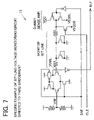
- FIG. 7 shows a circuit diagram of a bit-line-voltage monitoring circuit directed to the third embodiment
- FIG. 8 is an operational waveform diagram showing page operation (normal operation) of an asynchronous-type memory
- FIG. 9 is an operational waveform diagram showing late write function for page write operation of an asynchronous-type memory (fourth embodiment).
- FIG. 10 is an operational waveform diagram showing burst operation (normal operation) of a synchronous-type memory
- FIG. 11 is an operational waveform diagram showing late write function for burst write operation of a synchronous-type memory (fifth embodiment).
- FIG. 12 is a circuit block diagram showing a data-input/output path of a semiconductor memory device directed to related art
- FIG. 13 is an operational waveform diagram showing successive access operation directed to the related art
- FIG. 14 is circuit diagram of a data-input/output path wherein pre-charge period in related art is cut short.
- FIG. 15 is an operational waveform diagram of FIG. 14 .
- FIG. 1 shows an operational waveform diagram of successive access operation for illustrating principle of the present invention.
- Data of a plurality of bit lines connected to a plurality of memory cells due activation of a word line are set in a plurality of bit line pairs (BL 0 and /BlO, . . . , BLN and /BLN) and differentially amplified by sense amplifiers (not shown) up to voltage level of power source voltage VCC and ground voltage VSS. That is, when voltage level of the plurality of bit lines connected to the plurality of memory cells reach the power source voltage VCC or the ground voltage VSS, data-restore to each of the memory cells terminates and retention of data can be kept.
- bit lines BL 0 , . . . , BLN in high voltage level lowers whereas that of bit lines /BL 0 , . . . , /BL 0 in low voltage level rises. That is, so-called disturb phenomenon occurs.
- the voltage level against voltage interference due to disturb phenomenon may be amplification level that can avoid inversion of high-low voltage relation between bit lines. Not necessarily differential amplified up to full amplification level.
- a column selecting line CLO is driven in a form of pulse when differential amplification level of the bit line pair (BL 0 and /BL 0 ) reaches predetermined voltage so as to secure high-speed initial access for successive access operation.
- the bit line pair (BL 0 and /BL 0 ) receives disturb phenomenon.
- differential amplification of the bit line pairs (BL 0 and /BlO, . . . , BLN and /BLN) is continued even after completion of pulse drive of the column selecting line CL 0
- differential amplification of the bit line pair (BL 0 and /BL 0 ) is carried out accompanying recovery from the disturb phenomenon and after that, differential amplification of other bit line pairs (BL 1 and /BL 1 , . . . , BLN and /BLN) is also carried out. Consequently, the bit line pairs are differentially amplified up to full amplitude voltage level before second time of pulse drive with respect to the column selecting line CL 1 .
- column selecting lines CL 1 , . . . , CLN are driven in a form of pulse in order and corresponding bit line pair (BL 1 and /BL 1 , . . . , BLN and /BLN) and the data line pair (DB and /DB) are connected.
- bit line pair BL 1 and /BL 1 , . . . , BLN and /BLN
- DB and /DB data line pair
- a word line WL 0 currently activated is deactivated in appropriate timing taken between pulse drives of the column selecting lines CL 0 , . . . , CLN (in FIG. 1 , transition waveform indicated with broken line with respect to the word line WL 0 ) after the bit line pairs (BL 0 and /BL 0 , . . . , BLN and /BLN) are differentially amplified up to full amplitude voltage level.
- deactivation time ⁇ A of the word line can be embedded in ongoing successive data access operation.
- Pre-charge operation can be completed only taking deactivation time ⁇ B of the sense amplifier and equalizing time ⁇ C of the bit line pair. Thereby, a pre-charge period can be shortened.
- FIG. 2 is a circuit block diagram as to a data-input/output path of the semiconductor memory device of a First Embodiment.
- Memory cells C 00 and C 10 selected by a word line WL 0 are connected to bit lines BL 0 and BL 1 , respectively, and memory cells C 01 and C 11 selected by a word line WL 1 are connected to bit lines /BL 0 and /BL 1 , respectively.
- the word lines WL 0 and WL 1 are selected by decoding a row address (not shown) by a word decoder WD that is activated by a word line activating signal WLE.
- Data read out to the bit lines BL 0 and BL 1 , /BL 0 and /BL 1 are differentially amplified by a sense amplifier 0 (SA 0 ) and a sense amplifier 1 (SAl) as bit line pairs BLO and /BL 0 , BL 1 and /BL 1 .
- the sense amplifiers 0 and 1 (SA 0 , SA 1 ) are controlled by a sense amplifier activating signal SAE through a sense amplifier control circuit SAC.
- bit line pairs (BL 0 and /BL 0 , BL 1 and /BL 1 ) are controlled by column selecting lines CL 0 and CL 1 and electrically connected to data line pair (DB and /DB) through transfer gate pairs (T 0 Z and T 0 X, T 1 Z and T 1 X) so that a data access operation is carried out.
- the column selecting lines CL 0 and CL 1 are outputted from a column decoder 0 (CD 0 ) or a column decoder 1 (CD 1 ) that corresponds to a decoded column address (not shown), by a column-selection trigger signal CLE from a column-selection trigger circuit CLT.
- Data read out to the data line pair (DB and /DB) is amplified by a sense buffer SB and outputted from an input/output buffer IOBUF. Further, write data that is inputted to the input/output buffer IOBUF is written in the bit line pair (BL 0 and /BL 0 ) or (BL 1 and /BL 1 ) from a not-shown write amplifier through the data line pair (DB and /DB).
- a pre-charge control section 1 in the First Embodiment has a word line deactivating circuit WLR 1 for deactivating the word lines, a sense amplifier deactivating circuit SAR 1 for deactivating the sense amplifiers, and a bit line equalizing circuit BLR 1 for equalizing the bit line pairs.
- a delay circuit 1 ( 11 ) to which the sense amplifier activating signal SAE is inputted is connected and a delay signal SAED 1 in which delay time ⁇ 1 is added to the sense amplifier activating signal SAE is inputted as a control signal. Further, the column-selection trigger signal CLE is inputted to an inhibition (INH) terminal. From the word line deactivating circuit WLR 1 , the word line deactivating signal WLRST is outputted and further inputted to a word decoder WD and inputted to enable (EN) terminals of the sense amplifier deactivating circuit SAR 1 and the bit line equalizing circuit BLR 1 .
- the sense amplifier deactivating circuit SAR 1 is controlled by the pre-charge signal PRE and the sense amplifier deactivating signal SARST is outputted to the sense amplifier control circuit SAC. Further, to a preset (PST) terminal of the sense amplifier deactivating circuit SAR 1 , the sense amplifier activating signal SAE is inputted.
- bit line equalizing circuit BLR 1 To the bit line equalizing circuit BLR 1 , the delay circuit B (DB) to which the pre-charge signal PRE is inputted is connected and the delay signal ⁇ DB in which the delay time ⁇ B is added to the pre-charge signal PRE is inputted, and the bit line equalizing signal BLRST is outputted to the equalize control circuit EQC. Further, to the preset (PST) terminal of the bit line equalize circuit BLR 1 , a bit-line-equalizing cancel signal BLPC is inputted.
- bit-line-equalizing cancel signal BLPC is outputted and the bit line equalizing circuit BLR 1 is preset.
- the bit line equalizing signal BLRST is deactivated and it changes to a situation in which the enable (EN) terminal can accept the word line deactivating signal WLRST and the delay signal ⁇ DB.
- the sense amplifier activating signal SAE is activated and differential amplification of the bit line pairs (BL 0 and /BL 0 , BL 1 and /BL 1 ) is initiated.
- the sense amplifier deactivating circuit SAR 1 is preset and the sense amplifier deactivating signal SARST is deactivated, and it changes to a situation in which the enable (EN) terminal can accept the word line deactivating signal WLRST and the pre-charge signal PRE. Further, it is inputted to the delay circuit 1 ( 11 ) and timing length of the delay signal SAED 1 having the delay time ⁇ 1 is initiated.
- the delay time ⁇ 1 is of time from the input of the sense amplifier activating signal SAE until predetermined timing after the completion of the differential amplification of the bit line pairs (BL 0 and /BL 0 , BL 1 and /BL 1 ).
- This time is set to be a period in which pulse driving is not carried out as the deactivating period of the column-selection trigger signal CLE in the successive access operation.
- the column-selection trigger signal CLE is set to be the inhibition (INH) signal.
- the word line deactivating signal WLRST is outputted in wait for the completion of the pulse driving of the column-selection trigger signal CLE.
- the delay signal SAED 1 is outputted to the word line deactivating circuit WLR 1 .
- the column-selection trigger signal CLE is inputted to the inhibition (INH) terminal and therefore, the column-selection trigger signal CLE is not activated, and under a situation that the column selecting lines CL 0 and CL 1 are not pulse-driven, based upon the input of the delay signal SAED 1 , the word line deactivating signal WLRST is outputted.
- the word line WL 0 or WL 1 is deactivated before the initiation of the pre-charge period.
- the word line deactivating signal WLRST is a latch signal or a situation is latched after the signal is inputted to the enable (EN) terminals of the sense amplifier deactivating circuit SAR 1 and the bit line equalizing circuit BLR 1 . Further, in case that the word line deactivating signal WLRST is not the latch signal, it is preferable that the situation is latched also in the word decoder WD.
- the sense amplifier deactivating circuit SAR 1 and the bit line equalizing circuit BLR 1 are to be maintained in a situation in which the pre-charge signal PRE can be accepted.
- the pre-charge operation is initiated after the successive access operation is completed, since the pre-charge signal PRE is directly inputted to the sense amplifier deactivating circuit SAR 1 , the sense amplifier deactivating signal SARST is outputted immediately and deactivation of the sense amplifier is carried out.
- the bit line equalizing circuit BLR 1 since, to the bit line equalizing circuit BLR 1 , the pre-charge signal PRE is inputted through the delay circuit B (DB), after delay of delay time ⁇ B, the bit line equalizing signal BLRST is outputted and equalization of the bit line pairs (BL 0 and /BL 0 , BL 1 and /BL 1 ) is initiated.
- the delay time ⁇ B is of time for deactivating the sense amplifier. After the sense amplifier is surely deactivated, the equalizing operation of the bit line pairs is carried out, and thereby, unnecessary go-through current between the sense amplifier and the equalize circuit is prevented.
- FIG. 3 is a circuit diagram showing a specific example of the pre-charge control section 1 in First Embodiment.
- the delay circuit 1 ( 11 ) to which the sense amplifier activating signal SAE is inputted is constituted by even-number-stage inverter gate row and times the delay time ⁇ 1 .
- the delay signal SAED 1 outputted from the delay circuit 1 ( 11 ) is inputted to one of input terminals of a NAND gate.
- the column-selection trigger signal CLE is inputted from the inhibition (INH) terminal through the inverter gate.
- An output terminal of the NAND gate is connected to the inverter gate and an output signal from the inverter gate is latched by the latch circuit and the word line deactivating signal WLRST is outputted.
- the sense amplifier deactivating circuit SAR 1 has a NOR gate and, to one of input terminals thereof, the sense amplifier activating signal SAE is inputted from the preset (PST) terminal through the inverter gate. To the other input terminal, an output terminal of the inverter gate is connected, and to this inverter gate, a NAND gate is connected. To the NAND gate, the pre-charge signal PRE and the word line deactivating signal WLRST through the enable (EN) terminal are inputted.
- the sense amplifier deactivating signal SARST is outputted from an output terminal of a NOR gate through three-stage serially connected inverter gates.
- the bit line equalizing circuit BLR 1 has the same circuit structure as the sense amplifier deactivating circuit SAR 1 . It is of such a structure that a bit-line-equalizing cancel signal BLPC in place of the sense amplifier activating signal SAE in the sense amplifier deactivating circuit SAR 1 , and a delay signal ⁇ DB in place of the pre-charge signal PRE are inputted.
- FIG. 4 shows operational waveforms as to the First Embodiment ( FIG. 2 ) and the specific example ( FIG. 3 ) of its pre-charge control section 1 .
- the pre-charge signal PRE makes transition to low level and the successive access operation is initiated.
- the bit line equalizing circuit BLR 1 the bit-line-equalizing cancel signal BLPC makes transition to high level and thereby, the bit line equalizing signal BLRST set in high level to the bit-line-equalizing cancel signal BLPC in low level makes transition to low level so that the equalizing situation is canceled.
- the bit line equalizing signal BLRST is activated again during the pre-charge period, it is set to a preset situation, and it goes into a situation in which high level transition of the delay signal ⁇ DB can be accepted. Thereafter, by a not-shown control circuit, the word line activating signal WLE makes transition to high level and the word line WL 0 or WL 1 is activated through the word decoder WD. In addition, at this time point, the word line deactivating signal WLRST is in low level.
- the sense amplifier activating signal SAE makes transition to high level and the sense amplifiers are activated so that differential amplification of the bit line pairs (BL 0 and /BL 0 , BL 1 and /BL 1 ) is initiated.
- the sense amplifier deactivating circuit SAR 1 has the sense amplifier deactivating signal SARST make transition to low level so that the deactivating situation of the sense amplifiers is canceled. Then, since the sense amplifier deactivating signal SARST is activated again during the pre-charge period, it is set to the preset situation and goes into a situation in which high level transition of the pre-charge signal PRE can be accepted.
- a pulse signal in high level is outputted as an initial column-selection trigger signal CLE.
- the column selecting line CLO is driven as the pulse signal in high level, from the column decoder 0 (CD 0 ) and the bit line pair (BL 0 and /BL 0 ) is connected to the data line pair (DB 0 and /DB 0 ).
- voltage level of the bit line pair (BL 0 and /BL 0 ) is decreased due to the disturb phenomenon.
- the word line deactivating signal WLRST makes high level transition and deactivation of the word line WL 0 or WL 1 is carried out.
- the setting of the delay time ⁇ 1 is in principle carried out so that, after pulse driving of the initial column selecting line CLO and after completion of differential amplification to the bit line pair, the word line deactivating signal WLRST makes high level transition.
- the column-selection trigger signal CLE inputted to the inhibition (INH) terminal of the word line deactivating circuit WLR 1 , it is set so that it is not outputted during a period that the column-selection trigger signal CLE is inputted.
- the high level transition of the word line deactivating signal WLRST is made to be outputted after the pulse driving of the column selecting line and it is possible to sufficiently secure the restore level to the memory cell at the time of deactivation of the word lines.
- the word line deactivating signal WLRST is inputted to one of input terminals of the NAND gates through the enable (EN) terminals of the sense amplifier deactivating circuit SAR 1 and the bit line equalizing circuit BLR 1 . Therefor, by the high level change of the word line deactivating signal WLRST, it goes into a situation in which it is inputted to the other input terminals of the NAND gates of the both circuits SAR 1 and BLR 1 , and the pre-charge signal PRE and the delay signal ⁇ DB can be accepted.
- the sense amplifier deactivating signal SARST is outputted from the sense amplifier deactivating circuit SAR 1 .
- the sense amplifier activating signal SAE in high level situation sets one of input terminals of the NOR gate of the sense amplifier deactivating circuit SAR 1 through the inverter gate to low level. Therefore, by the high level transition of the other input terminal of the NOR gate due to the high level transition of the pre-charge signal PRE, the sense amplifier deactivating signal SARST makes high level transition. That is, due to the high level transition of the pre-charge signal PRE by the initiation of the pre-charge period, the sense amplifiers are deactivated.
- the bit line equalizing circuit BLR 1 Since the bit line equalizing circuit BLR 1 has the same circuit structure as the sense amplifier deactivating circuit SAR 1 , by the high level transition of the delay signal ⁇ DB, the bit line equalizing signal BLRST makes high level transition so that the equalizing operation of the bit line pair is initiated.
- the delay signal ⁇ DB for initiating the equalizing operation of the bit line pair is of a delay signal to which delay of the delay time ⁇ B is added from the pre-charge signal PRE through the delay circuit B (DB). Accordingly, the initiation of the bit line equalizing operation (the high level transition of BLRST) is delayed by the delay time ⁇ B to the initiation of the deactivation of the sense amplifier (the high level transition of SARST). In case that this delay time ⁇ B is set to be a predetermined time for deactivation of the sense amplifier, the equalizing operation of the bit line pair is to be carried out following the completion of the deactivation of the sense amplifier.
- the low level transition of the sense amplifier activating signal SAE is carried out.
- the delay signal SAED 1 is changed to low level.
- the word line deactivating signal WLRST make low level transition in preparation of a next access operation.
- a word line deactivating circuit WLR 2 is provided in place of the word line deactivating circuit WLR 1 in the pre-charge control section 1 (FIG. 2 ) of the First Embodiment, a word line deactivating circuit WLR 2 is provided and further, a column-selection-time detecting circuit 22 is provided.
- the column-selection-time detecting circuit 22 outputs a detection signal CLDT in case that the column-selection trigger signal CLE to be inputted reaches a predetermined number of times.
- the detection signal CLDT is supplied to the word line deactivating circuit WLR 2 through a delay circuit 2 ( 12 ) that times delay time ⁇ 2 .
- a delay circuit 2 ( 12 ) that times delay time ⁇ 2 .
- the delay time ⁇ 2 it is possible to time appropriate timing up to before a final column selection trigger signal CLE is outputted, to the detection signal CLDT outputted in case that the predetermined number of the column-selection trigger signal CLE is detected.
- the number of column selection which is detected by the column-selection-time detecting circuit 22 can be set to be 1 or larger, up to the number of times that 1 is subtracted from the number of all selection times, or, for burst length NBL, 1 or larger, up to the number of times of (NBL ⁇ 1) or smaller.
- the former is the setting for the page mode in which, in response to the transition of the column address, the address access is carried out and the corresponding column selecting line is selected sequentially
- the latter is the setting for the burst mode in which, based upon the initial column address, the column selecting line is sequentially and automatically selected.
- NBL burst length
- the maximum countable number in the column-selection-time detecting circuit 22 can be set. Further, in case that the successive access number is uncertain, it is possible to correspond thereto by setting that the initial column selection is detected in the column-selection-time detecting circuit 22 .
- the delay time ⁇ 2 is set to be of time from the detected column-selection trigger signal CLE until initiation of an adjacent column-selection trigger signal CLE and (NBL ⁇ 1)th column selection that is the maximum countable value in the column-selection-time detecting circuit 22 is detected.
- the write operation since the number of successive accesses is uncertain, the number of column selecting lines which are selected after the deactivation of the word line is made to be uncertain.
- the page mode when the word line is activated in one time of the successive access operation, total number (N) of the bit line pairs deferentially amplified is determined in advance and this total number (N) is the total number of column selection lines that are selected. Accordingly, to the write operation after the word line is deactivated in advance, it is structured that (N ⁇ 1) sets of the temporary storage registers are provided and in the same manner as in the case of the burst mode, the additional write operation can be carried out in the time region for refresh operation after the completion of the successive access operation.
- a word line deactivating circuit WLR 3 is provided in place of the word line deactivating circuit WLR 2 in the pre-charge control section 2 ( FIG. 5 ) of the Second Embodiment. Further, in place of the delay circuit 1 ( 11 ) of the First and Second Embodiments ( FIGS. 2 and 5 ), a bit-line-voltage monitoring circuit 13 is provided.
- the sense amplifier activating signal SAE and the column-selection trigger signal CLE are inputted, and as a result of monitoring the bit line voltage, the detection signal BLF is outputted to the word line deactivating circuit WLR 3 .
- FIG. 7 shows a concrete example of the bit-line-voltage monitoring circuit 13 .
- a comparator in which a bias current flows in response to the sense amplifier activating signal SAE of high level is provided, and to one of input terminals thereof, reference voltage VRF which is divided by registers is connected. To the other input terminal, one end of a monitor bit line is connected so that the bit line voltage VDBL is detected.
- the monitor bit line has an equivalent physical structure to the real bit line and has an equivalent load structure.
- a NMOS transistor which is equivalent to a NMOS transistor for switching which configures the memory cell is connected to in addition to connecting layout in the real bit line. Since this NMOS transistors simulate load in the real bit line, a gate terminal is connected to a source terminal and biased to ground voltage so that an off situation is maintained.
- the resistor component between connecting nodes of the NMOS transistors is of one which wiring resistor of the monitor bit line is explicitly described. Since it has the equivalent physical structure to the real bit line, it has an equivalent resistor value.
- a dummy sense amplifier provided at the other end of the monitor bit line is of a circuit structure that simulates differential amplification of the real bit line by the sense amplifier.
- a connection is carried out from the monitor bit line to power source voltage VCC through a PMOS transistor and to equalizing voltage VEQBL of the bit lines through the NMOS transistor.
- the PMOS/NMOS transistors that configure the dummy sense amplifier have an equivalent driving ability to transistors that configure the sense amplifier.
- the equalizing voltage VEQBL is, for example, (1 ⁇ 2) VCC voltage.
- SAE To gate terminals of the PMOS/NMOS transistors, the sense amplifier activating signal SAE is inputted through the inverter gate.
- the NMOS transistor is turned on and the monitor bit line is initialized to the equalizing voltage VEQBL.
- the PMOS transistor is turned on and the monitor bit line is charged up to the power voltage VCC. It simulates a high level side bit line pair among the bit line pairs differentially amplified.
- the NMOS transistor that is controlled by the column-selection trigger signal CLE turned on during the high level pulse driving period, and electrically connects the monitor bit line to voltage VEQDB, simulates the disturb phenomenon to the bit line when the bit line is connected to the data line.
- the voltage VEQDB is of a voltage central value of the data line that is amplitude-limited and for example, (1 ⁇ 2) VCC voltage.
- the output terminal of the comparator makes low level transition and is inverted by the inverter gate and high level detection signal BLF is outputted.
- the reference voltage VRF is set to be of a voltage by which the bit line pair is sufficiently differentially amplified, and re-write of sufficient restore voltage to the memory cells is possible.
- Operational waveforms of Fourth Embodiment shown in FIG. 9 show operational waveforms that are applied to the case (page write operation) in which a page operation of an asynchronous-type memory is a write operation. It is the case that has a so-called late write function in which the write operation after the word line is deactivated in advance is additionally written in a time region which is secured for refreshing.
- a first operation cycle is an operation cycle of the page write operation.
- the operation is initiated by low level change of /CE 1 as a trigger and a row address AR 0 is taken in as an address signal ADD and operation of row system is initiated.
- the word line WL 0 that is selected by decoding the row address AR 0 is activated and data of the memory cells are read out to the bit lines and the differential amplification is carried out by the sense amplifiers (WLSL).
- corresponding column selecting lines CL 0 through CL 3 are activated by high level pulses, and the bit line pair which corresponds to each column address is connected to the data line pair so that write of data is carried out from outside (WR 0 through WR 3 ).
- a second operation cycle is of the case that read-out operation is carried out as the page operation (page read operation). It is an equivalent operation to the page write operation.
- a word line WL 10 which is selected by a row address AR 10 is activated by low level change of /CE 1 as a trigger (WLSL), and thereafter, based upon low level change of /OE, column selecting lines CL 10 through CL 13 which correspond to column addresses AC 10 through AC 13 are activated and successive data read-out is carried out (RD 10 through RD 13 ).
- a third operation cycle is a normal read operation in which normal single bit read-out cycle is carried out.
- a word line WL 20 that is selected by a row address AR 20
- a column selecting line CL 20 which corresponds to a column address AC 20 is activated and read-out of single bit data is carried out.
- the number of successive accesses can be increased and decreased appropriately in response to the change of column addresses.
- FIG. 8 a case in which the successive access operation is carried out for four column address changes is described as one example. It requires tPW as a cycle time of the page write operation and tPR as a cycle time of the page read operation.
- time regions ((I) through (III)) for refreshing provided between any two of the three operation cycles, namely, first operation cycle, second operation cycle, and third operation cycle.
- a refresh cycle is of long cycle as compared with the normal operation cycle and for example, one refreshing operation is carried out for 1000 times of access operations that are carried out in several 10 nsec.
- the refreshing operation is carried out in all time regions between operation cycles. In case that it coincides with the refreshing cycle, it is carried out in any one time region among the time regions of ((I) through (III)), and a standby situation is maintained in other time regions.
- a word line WLRef which is different from before-and-after normal access operations is activated and therefore, it is necessary to set a pre-charge period tPR for switching the word line. During this period, switching of the word line, the deactivation operation of the sense amplifier based upon this and the equalizing operation of the bit line pair are carried out.
- the first and second operation cycles are shown as the page write operation.
- the word lines WL 0 and WL 10 are deactivated after selection of the column selecting lines CL 3 and CL 13 as to the fourth column addresses AC 3 and AC 13 , and in contrast, in Fourth Embodiment, the deactivation is carried out after selection of the column selecting lines CL 2 and CL 12 by the third column addresses AC 2 and AC 12 .
- column addresses AC 3 and AC 13 are stored in address registers RGA( 1 ) and RGA( 2 ), corresponding write data is stored in write data registers RGD( 1 ) and RGD( 2 ) and an additional write operation is carried out in the time region for refresh operation after the completion of the page write operation.
- additional write since it is general that word lines to be activated are different, it is preferable to store also row addresses which are activated in the page write operation in the address registers RGA( 1 ) and RGA( 2 ).
- an address register and a write data register are provided in response to the number of column selecting lines which are selected after the deactivation of the word line.
- the number of column selecting lines which are selected after the deactivation of the word line is assumed to be 5.
- the page write operation is carried out successively and the refreshing operation is carried out during the periods adjoining each other, it is possible to realize a late write function in case that 10 sets of registers for temporary storage are provided.
- a semiconductor memory such as a pseudo-SRAM and so on in which an external access operation such as data read-out and write etc. and the refreshing operation are carried out independently
- contemplated is a case in which an external-access-start request signal competes with a refresh-start request signal.
- cycle time tCE is defined by arranging the external access operation and the refreshing operation in one operation cycle as one series of operation.
- the refreshing operation is not actually carried out in a time region for refreshing operation at this time, and it is possible to carry out the additional write operation through the use of this time region.
- the pre-charge period can be shortened and the cycle time of the page operation can be shortened. This advantage can be applied not only to the page read operation but also to the page write operation through the use of the above-described late write function.
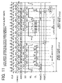
- Operational wave forms of Fifth Embodiment shown in FIG. 11 shows operational wave forms that the invention is applied to a case (burst write operation) in which the burst operation of the asynchronous-type memory is the write operation.
- This is the case that has the so-called late write function in which the write operation after the word line is deactivated in advance is additionally carried out in a time region which is secured for refreshing.
- FIG. 10 is a timing chart of CAS latency 1 . This is a case that as for the burst write operation and the burst read operation, the burst operation is carried out by commands (WRA command and RDA command) with an automatic pre-charge operation. This shows a case that burst length is 8.
- a burst write cycle and burst read cycle are configured by 12 clocks (CLK), concurrently.
- FIG. 11 there are waveforms as to a synchronous-type semiconductor memory in which, by providing an operational specification for imbedding a time region for refreshing operation in the burst read operation, without discontinuing the burst operation, the refreshing operation can be carried out, and which has also the late write function.
- Conditions of the burst operation in FIG. 11 are, in the same manner as in the case of FIG. 10 , of CAS latency 1 , burst length 8 and burst operation by the command (WRA command and RDA command) with the automatic pre-charge operation.
- column selecting lines CL 10 through CL 17 in the burst read operation are not synchronized with the clock CLK and hereby, selection is carried out at fast cycle. That is, in advance of timing of the clock CLK, the bit line pair and the data line pair are electrically connected and data is to be read out to the data line pair. It is specified that the data which was read out in advance is stored in a temporary storage circuit such as a data buffer circuit and so on and is to be outputted to outside in synchronous with the clock CLK which is read-out timing thereafter.
- the burst write operation in the same manner as in the case of FIG. 10 , the burst operation is carried out at timing that is synchronized with the clock. In order to deactivate the word line in advance, the burst write operation is completed without carrying out the write to the column selecting line CL 7 .
- the column address that is not written in and write data are kept in the address register RGA( 1 ) for temporary storage and the write data register RGD( 1 ). At this time, it is preferable to keep row address in the address register RGA( 1 ).
- the address and write data which are kept in the registers RGA( 1 ) and RGD( 1 ) can be additionally written in the time region which is imbedded in the burst read operation.
- the burst write cycle can be of 11 clocks in 1 clock shortened, whereas it is of 12 clocks in normal case.
- the burst read cycle since the column selecting lines CL 10 through CL 17 can be selected in advance of the clock CLK, the number of cycle clock can be reduced in the same manner. It is possible to realize the shortening of the burst operation.
- the word lines WL 0 , WL 1 and WL 10 are connected to a plurality of memory cells and wiring length is lengthened, and even in case that time constant of voltage transition is increased on the occasion of the deactivation, time constant of the deactivation of the word lines WL 0 , WL 1 and WL 10 are not to be added during the pre-charge period and it is possible to shorten the pre-charge period. Accordingly, proportion of the pre-charge period to the access period for the memory cells can be compressed, and it is possible to shorten the cycle time and to improve an occupied ratio of the data access operation which is occupied in the operation period of the semiconductor memory device.
- the additional write cycle for executing the late write operation may be carried out during a clock suspend mode, a power down mode and so on, which are operation modes in which, without carrying out the external access operation, it is known in advance that NOP cycle of a given time continues.
- the deactivating operation of the word lines WL 0 , WL 1 and WL 10 is carried out in case that the word line activating circuits WLR 1 through WLR 3 are activated, in the successive access operation, in such a situation that the column-selection trigger circuit CLT which is the column selection section does not output the column-selection trigger signal CLE.
- the deactivating operation of the word lines WL 0 , WL 1 and WL 10 can be carried out, by avoiding a period that a plurality of bit lines receive the disturb phenomenon during column selection, at a time point that, after completion of the column selection, restore to the plurality of memory cells is completed. It is possible to shorten the pre-charge period without aggravating retention of data that is stored in the plurality of memory cells.
- bit lines BL 0 and BL 1 or /BL 0 and /BL 1 are amplified to a voltage level in which logical level of data is not reversed even in case of the disturb phenomenon. Accordingly, as an initial data access speed in the successive access operation is maintained in high speed, the deactivating operation of the word lines WL 0 , WL 1 and WL 10 is carried out during the successive access operation and thereby, it is possible to shorten the pre-charge period.
- time from activation of the successive access operation until completion of differential amplification of data in a plurality of the bit line pairs is inherent time by a circuit structure of the semiconductor memory device, physical condition and so on, and further, period between the column-selection trigger signals CLE in the successive access operation is time that is defined in response to the time which is inherent to the semiconductor memory device or the operational specification thereof, and thereby, this time is timed as the delay time ⁇ 1 which is first predetermined delay time, or the delay time ⁇ 2 that is second predetermined delay time so that a predetermined timing after completion of differential amplification in the plurality of bit line pairs can be timed.
- the delay time ⁇ 1 can be timed by the delay circuit 1 ( 11 ) that is a first delay circuit
- the delay time ⁇ 2 can be timed by the delay circuit 2 ( 12 ) that is a second delay circuit.
- the delay time ⁇ 2 is of one that times the predetermined time from completion of the anterior column-selection trigger signal CLE that is a first column selection until before initiation of the posterior column-selection trigger signal CLE that is a second column selection. It is possible that the precedent and following column-selection signals CLE are made to be adjacent trigger signals, and intermediate time during that period is timed.
- the case of the inherent time due to the circuit structure of the semiconductor memory device and the operational specification is, for example, the access operation in the burst mode
- the case of the time defined in response to the input/output specification is, for example, a case in which data access is carried out in response to change of column address inputted from outside and access commands.
- the word line activating signal WLE means a signal including, in addition to activating operation of the word lines WL 0 , WL 1 and WL 10 or its control signal, an operation relating to activation of the word lines WL 0 , WL 1 and WL 10 or its control signal, and a predetermined operation which is carried out at a predetermined timing to the activation of the word lines WL 0 , WL 1 and WL 10 or its control signal.
- the sense amplifier activating signal SAE which is a signal for initiating the differential amplification of data means a signal including, in addition to the activating operation of the sense amplifier or its control signal, an operation relating to the initiation of the differential amplification or its control signal, and a predetermined operation which is carried out at a predetermined timing to the initiation of the differential amplification or its control signal.
- an operation of row series it is a signal including a series of operations that are carried out at a predetermined timing or its control signal.
- the semiconductor memory device which carries out the burst operation it is possible to set appropriately the anterior column-selection trigger signal CLE out of trigger signals below (burst length ⁇ 1)th time. Furthermore, it is possible to set to a trigger signal CLE of (burst length ⁇ 1)th time which is a trigger signal CLE of one before a final column-selection trigger signal CLE. In this case, in a trigger signal CLE other than the final column-selection trigger signal CLE, the word lines WL 0 , WL 1 and WL 10 are in activated situation and it is possible to flexibly correspond also to the successive write operation.
- a plurality of bit lines BL 0 and BL 1 , or /BL 0 and /BL 1 are electrically connected to a plurality of memory cells C 00 and C 10 or C 01 and C 11 , it is possible to deactivate the word line WL 0 or WL 1 at inherent minimum time which is determined by the circuit structure of the semiconductor memory device, the physical condition and so on, by deactivating the word line WL 0 or WL 1 at time point that data restoration to the plurality of memory cells C 00 and C 10 or C 01 and C 11 is completed.
- the word line WL 0 or WL 1 can be deactivated, and in the page operation in which length of the successive access is not fixed, it is possible to shorten the pre-charge period regardless of the length of successive access.
- the word lines WL 0 , WL 1 and WL 10 can be deactivated, and in the page operation in which length of the successive access is not fixed, it is possible to shorten the pre-charge period regardless of the length of successive access.
- a predetermined combination as to the delay circuit 1 ( 11 ), the column-selection-time detecting circuit 22 and the bit-line-voltage monitoring circuit 13 was exemplified but in the invention, it is not limited to this combination and it is possible to configure by use of respective ones independently. Further, it is possible to use them in an appropriate combination other than the exemplified one.
- the page operation was described as the successive access operation of the asynchronous-type memory and the burst operation was described as the successive access operation of the synchronous-type memory, but it goes without saying that the invention can be applied to a case in which the burst operation function is applied to the asynchronous-type memory and a case in which the page operation is applied to the synchronous-type memory.
- the burst operation to the asynchronous-type memory is of a case having an operation in which an internal counter and so on are provided, and based upon an input of an initial column address, an access point is switched sequentially.
- the page operation to the synchronous-type memory is of a case in which the read command and the write command continue.
- activation of a word line or word line activating signal includes activating operation of a word line or its control signal, correlative operations for activation of word lines or theirs control signals, and predetermined operation to be carried out for activation of a word line with predetermined timing or its control signal, respectively.
- initiation of data amplification or an initializing signal for data amplification includes initializing operation for amplifying circuit such as a sense amplifier or its control signal or the like, operation for starting data amplification or its control signal, and predetermined operation to be carried out for initializing data amplification with predetermined timing or its control signal, respectively.
- Operation for row system includes sequential operations carried out with predetermined timing or its control signal.
- selection of first column selection or the first column selecting section may be set to (burst length ⁇ 1)th column selection that is precedent to last column selection in successive access operation so that column selections other than the last column selection can be put on active state. This is preferable for write operation.
- the word line can be deactivated prior to ongoing successive access operation and pre-charge period can be shortened regardless of successive access length during page mode where length of successive access operation is uncertain.
- successive access operation is successive data write operation
- write operation to column selection after deactivation of a word line it is preferable that address and write data are temporarily stored.
- a period of successive data write operation is shorter than a refresh period, therefore, out of time region secured for refresh operation, a part of the time region where refresh operation is not carried out can be utilized for additional data write operation.
- a temporary storing region or address register group and a write-data register group it may be structured such that column address corresponding to memory cell groups as many as a number obtained by subtracting 1 from the number of memory cells selected by a word line to be activated can be stored.
- a word line can be deactivated with proper timing regardless of length of successive access.
- burst mode for write operation where length of successive access is determined, a word line can be deactivated with proper timing.
- additional write operation may be carried out successively so that additional write operation can be carried out with high-speed.
- deactivation of the word line which was carried out during the pre-charge period is carried out in advance, and thereby, without any deterioration of the restore voltage to the memory cell and any delay of an initial data access time, it is possible to shorten the pre-charge period after the successive access operation.
Landscapes
- Engineering & Computer Science (AREA)
- Microelectronics & Electronic Packaging (AREA)
- Computer Hardware Design (AREA)
- Dram (AREA)
Applications Claiming Priority (2)
| Application Number | Priority Date | Filing Date | Title |
|---|---|---|---|
| JP2002-106344 | 2002-04-09 | ||
| JP2002106344A JP4544808B2 (ja) | 2002-04-09 | 2002-04-09 | 半導体記憶装置の制御方法、および半導体記憶装置 |
Publications (2)
| Publication Number | Publication Date |
|---|---|
| US20030191974A1 US20030191974A1 (en) | 2003-10-09 |
| US7142468B2 true US7142468B2 (en) | 2006-11-28 |
Family
ID=28672414
Family Applications (1)
| Application Number | Title | Priority Date | Filing Date |
|---|---|---|---|
| US10/299,713 Expired - Fee Related US7142468B2 (en) | 2002-04-09 | 2002-11-20 | Control method of semiconductor memory device and semiconductor memory device |
Country Status (5)
| Country | Link |
|---|---|
| US (1) | US7142468B2 (ja) |
| JP (1) | JP4544808B2 (ja) |
| KR (1) | KR100864036B1 (ja) |
| CN (1) | CN1258188C (ja) |
| TW (1) | TW594750B (ja) |
Cited By (3)
| Publication number | Priority date | Publication date | Assignee | Title |
|---|---|---|---|---|
| US20110188314A1 (en) * | 2010-01-29 | 2011-08-04 | Kuo Tien-Chien | Bit line stability detection |
| US9460766B2 (en) | 2014-09-05 | 2016-10-04 | Samsung Electronics Co., Ltd. | Memory device, and memory system including the same |
| US10796732B2 (en) | 2018-12-21 | 2020-10-06 | Toshiba Memory Corporation | Semiconductor storage device |
Families Citing this family (12)
| Publication number | Priority date | Publication date | Assignee | Title |
|---|---|---|---|---|
| KR100555534B1 (ko) * | 2003-12-03 | 2006-03-03 | 삼성전자주식회사 | 인액티브 위크 프리차아징 및 이퀄라이징 스킴을 채용한프리차아지 회로, 이를 포함하는 메모리 장치 및 그프리차아지 방법 |
| KR100551485B1 (ko) * | 2003-12-04 | 2006-02-13 | 삼성전자주식회사 | 메모리 장치의 타이밍 제어 방법 |
| KR100733420B1 (ko) | 2005-06-30 | 2007-06-29 | 주식회사 하이닉스반도체 | 동기식 반도체 메모리 장치 |
| US7944764B1 (en) * | 2008-12-31 | 2011-05-17 | Micron Technology, Inc. | Writing to non-volatile memory during a volatile memory refresh cycle |
| US8675418B2 (en) * | 2010-08-31 | 2014-03-18 | Taiwan Semiconductor Manufacturing Company, Ltd. | Memory write assist |
| CN103166605B (zh) * | 2013-01-25 | 2016-04-06 | 江苏芯力特电子科技有限公司 | 一种多相非交叠时钟电路 |
| KR20160100584A (ko) * | 2015-02-16 | 2016-08-24 | 에스케이하이닉스 주식회사 | 반도체 메모리 장치 및 그의 테스트 방법 |
| KR20160124582A (ko) * | 2015-04-20 | 2016-10-28 | 에스케이하이닉스 주식회사 | 센스앰프 및 이를 포함하는 반도체 장치 |
| JP2019102106A (ja) * | 2017-11-28 | 2019-06-24 | ルネサスエレクトロニクス株式会社 | 半導体装置 |
| CN111179990B (zh) * | 2019-12-31 | 2021-07-27 | 展讯通信(上海)有限公司 | 写操作辅助电路 |
| US20210303215A1 (en) * | 2020-03-27 | 2021-09-30 | Etron Technology, Inc. | Memory controller, memory, and related memory system |
| CN112509620A (zh) * | 2020-11-30 | 2021-03-16 | 安徽大学 | 基于平衡预充与组译码的数据读取电路 |
Citations (8)
| Publication number | Priority date | Publication date | Assignee | Title |
|---|---|---|---|---|
| JPH06176568A (ja) | 1992-12-07 | 1994-06-24 | Fujitsu Ltd | 半導体記憶装置 |
| JPH09161477A (ja) | 1995-12-11 | 1997-06-20 | Mitsubishi Electric Corp | 半導体記憶装置 |
| US5668774A (en) * | 1995-05-22 | 1997-09-16 | Mitsubishi Denki Kabushiki Kaisha | Dynamic semiconductor memory device having fast operation mode and operating with low current consumption |
| US5729504A (en) * | 1995-12-14 | 1998-03-17 | Micron Technology, Inc. | Continuous burst edo memory device |
| JPH10312684A (ja) | 1997-05-13 | 1998-11-24 | Fujitsu Ltd | 半導体集積回路 |
| US6229758B1 (en) * | 1999-09-16 | 2001-05-08 | Matsushita Electric Industrial Co., Ltd. | Semiconductor memory device that can read out data faster than writing it |
| JP2001236798A (ja) | 2000-02-18 | 2001-08-31 | Fujitsu Ltd | 半導体記憶装置及びストレス電圧設定方法 |
| US6442088B1 (en) * | 1998-05-07 | 2002-08-27 | Kabushiki Kaisha Toshiba | Semiconductor memory system, and access control method for semiconductor memory and semiconductor memory |
Family Cites Families (7)
| Publication number | Priority date | Publication date | Assignee | Title |
|---|---|---|---|---|
| JPH03105787A (ja) * | 1989-09-19 | 1991-05-02 | Nec Ic Microcomput Syst Ltd | 半導体集積回路 |
| JPH0490190A (ja) * | 1990-08-01 | 1992-03-24 | Sharp Corp | 半導体記憶装置 |
| JPH06349280A (ja) * | 1993-06-11 | 1994-12-22 | Matsushita Electric Ind Co Ltd | 半導体記憶装置 |
| JP2894170B2 (ja) * | 1993-08-18 | 1999-05-24 | 日本電気株式会社 | メモリ装置 |
| JP3222684B2 (ja) * | 1994-04-20 | 2001-10-29 | 株式会社東芝 | 半導体記憶装置 |
| JPH08102187A (ja) * | 1994-09-29 | 1996-04-16 | Toshiba Microelectron Corp | ダイナミック型メモリ |
| JP2001067866A (ja) * | 1999-08-30 | 2001-03-16 | Mitsubishi Electric Corp | 同期型半導体記憶装置 |
-
2002
- 2002-04-09 JP JP2002106344A patent/JP4544808B2/ja not_active Expired - Fee Related
- 2002-11-20 US US10/299,713 patent/US7142468B2/en not_active Expired - Fee Related
- 2002-11-21 TW TW091133975A patent/TW594750B/zh not_active IP Right Cessation
- 2002-12-11 KR KR1020020078649A patent/KR100864036B1/ko not_active IP Right Cessation
-
2003
- 2003-01-16 CN CNB031015115A patent/CN1258188C/zh not_active Expired - Fee Related
Patent Citations (9)
| Publication number | Priority date | Publication date | Assignee | Title |
|---|---|---|---|---|
| JPH06176568A (ja) | 1992-12-07 | 1994-06-24 | Fujitsu Ltd | 半導体記憶装置 |
| US5668774A (en) * | 1995-05-22 | 1997-09-16 | Mitsubishi Denki Kabushiki Kaisha | Dynamic semiconductor memory device having fast operation mode and operating with low current consumption |
| JPH09161477A (ja) | 1995-12-11 | 1997-06-20 | Mitsubishi Electric Corp | 半導体記憶装置 |
| US5729504A (en) * | 1995-12-14 | 1998-03-17 | Micron Technology, Inc. | Continuous burst edo memory device |
| JPH10312684A (ja) | 1997-05-13 | 1998-11-24 | Fujitsu Ltd | 半導体集積回路 |
| US6026034A (en) * | 1997-05-13 | 2000-02-15 | Fujitsu Limited | Bit line reset circuit of memory |
| US6442088B1 (en) * | 1998-05-07 | 2002-08-27 | Kabushiki Kaisha Toshiba | Semiconductor memory system, and access control method for semiconductor memory and semiconductor memory |
| US6229758B1 (en) * | 1999-09-16 | 2001-05-08 | Matsushita Electric Industrial Co., Ltd. | Semiconductor memory device that can read out data faster than writing it |
| JP2001236798A (ja) | 2000-02-18 | 2001-08-31 | Fujitsu Ltd | 半導体記憶装置及びストレス電圧設定方法 |
Cited By (6)
| Publication number | Priority date | Publication date | Assignee | Title |
|---|---|---|---|---|
| US20110188314A1 (en) * | 2010-01-29 | 2011-08-04 | Kuo Tien-Chien | Bit line stability detection |
| US8116139B2 (en) | 2010-01-29 | 2012-02-14 | Sandisk Technologies Inc. | Bit line stability detection |
| USRE45567E1 (en) | 2010-01-29 | 2015-06-16 | Sandisk Technologies Inc. | Bit line stability detection |
| US9460766B2 (en) | 2014-09-05 | 2016-10-04 | Samsung Electronics Co., Ltd. | Memory device, and memory system including the same |
| US10796732B2 (en) | 2018-12-21 | 2020-10-06 | Toshiba Memory Corporation | Semiconductor storage device |
| US11100961B2 (en) | 2018-12-21 | 2021-08-24 | Kioxia Corporation | Semiconductor storage device |
Also Published As
| Publication number | Publication date |
|---|---|
| JP2003303493A (ja) | 2003-10-24 |
| CN1258188C (zh) | 2006-05-31 |
| US20030191974A1 (en) | 2003-10-09 |
| JP4544808B2 (ja) | 2010-09-15 |
| KR20030080991A (ko) | 2003-10-17 |
| TW594750B (en) | 2004-06-21 |
| TW200305162A (en) | 2003-10-16 |
| KR100864036B1 (ko) | 2008-10-16 |
| CN1450558A (zh) | 2003-10-22 |
Similar Documents
| Publication | Publication Date | Title |
|---|---|---|
| JP5633887B2 (ja) | 行および列へのアクセス動作を同期させるための方法および装置 | |
| US6826104B2 (en) | Synchronous semiconductor memory | |
| US7142468B2 (en) | Control method of semiconductor memory device and semiconductor memory device | |
| US6831853B2 (en) | Apparatus for cleaning a substrate | |
| KR100776612B1 (ko) | 반도체 기억 장치 | |
| JPH0527194B2 (ja) | ||
| US7349274B2 (en) | Precharge circuit and method employing inactive weak precharging and equalizing scheme and memory device including the same | |
| WO2003003376A1 (en) | System and method for early write to memory by holding bitline at fixed potential | |
| US6067270A (en) | Multi-bank memory devices having improved data transfer capability and methods of operating same | |
| US9324414B2 (en) | Selective dual cycle write operation for a self-timed memory | |
| US6714463B2 (en) | Semiconductor memory device having reduced chip select output time | |
| US6487132B2 (en) | Integrated circuit memory devices having multiple input/output buses and precharge circuitry for precharging the input/output buses between write operations | |
| JP2698232B2 (ja) | 半導体記憶装置 | |
| EP1132923B1 (en) | Bit line sense circuit and method for dynamic random access memories | |
| KR100724517B1 (ko) | 반도체 기억 장치 | |
| JP2729302B2 (ja) | 半導体記憶装置におけるデータ転送方法 | |
| JPS6235193B2 (ja) | ||
| CA2803037A1 (en) | Method and apparatus for synchronization of row and column access operations | |
| JP2000348489A (ja) | 半導体記憶装置及びその駆動方法 | |
| KR20030078309A (ko) | 향상된 프리차지 타임을 가지기 위한 메모리 장치 |
Legal Events
| Date | Code | Title | Description |
|---|---|---|---|
| AS | Assignment |
Owner name: FUJITSU LIMITED, JAPAN Free format text: ASSIGNMENT OF ASSIGNORS INTEREST;ASSIGNORS:KATO, YOSHIHARU;KAWAMOTO, SATORU;REEL/FRAME:013505/0116 Effective date: 20021023 |
|
| FEPP | Fee payment procedure |
Free format text: PAYOR NUMBER ASSIGNED (ORIGINAL EVENT CODE: ASPN); ENTITY STATUS OF PATENT OWNER: LARGE ENTITY |
|
| AS | Assignment |
Owner name: FUJITSU MICROELECTRONICS LIMITED, JAPAN Free format text: ASSIGNMENT OF ASSIGNORS INTEREST;ASSIGNOR:FUJITSU LIMITED;REEL/FRAME:021998/0645 Effective date: 20081104 Owner name: FUJITSU MICROELECTRONICS LIMITED,JAPAN Free format text: ASSIGNMENT OF ASSIGNORS INTEREST;ASSIGNOR:FUJITSU LIMITED;REEL/FRAME:021998/0645 Effective date: 20081104 |
|
| FPAY | Fee payment |
Year of fee payment: 4 |
|
| AS | Assignment |
Owner name: FUJITSU SEMICONDUCTOR LIMITED, JAPAN Free format text: CHANGE OF NAME;ASSIGNOR:FUJITSU MICROELECTRONICS LIMITED;REEL/FRAME:024982/0245 Effective date: 20100401 |
|
| FPAY | Fee payment |
Year of fee payment: 8 |
|
| AS | Assignment |
Owner name: SOCIONEXT INC., JAPAN Free format text: ASSIGNMENT OF ASSIGNORS INTEREST;ASSIGNOR:FUJITSU SEMICONDUCTOR LIMITED;REEL/FRAME:035508/0337 Effective date: 20150302 |
|
| FEPP | Fee payment procedure |
Free format text: MAINTENANCE FEE REMINDER MAILED (ORIGINAL EVENT CODE: REM.) |
|
| LAPS | Lapse for failure to pay maintenance fees |
Free format text: PATENT EXPIRED FOR FAILURE TO PAY MAINTENANCE FEES (ORIGINAL EVENT CODE: EXP.); ENTITY STATUS OF PATENT OWNER: LARGE ENTITY |
|
| STCH | Information on status: patent discontinuation |
Free format text: PATENT EXPIRED DUE TO NONPAYMENT OF MAINTENANCE FEES UNDER 37 CFR 1.362 |
|
| FP | Lapsed due to failure to pay maintenance fee |
Effective date: 20181128 |