US7115446B2 - Flip chip bonding method for enhancing adhesion force in flip chip packaging process and metal layer-built structure of substrate for the same - Google Patents
Flip chip bonding method for enhancing adhesion force in flip chip packaging process and metal layer-built structure of substrate for the same Download PDFInfo
- Publication number
- US7115446B2 US7115446B2 US10/964,371 US96437104A US7115446B2 US 7115446 B2 US7115446 B2 US 7115446B2 US 96437104 A US96437104 A US 96437104A US 7115446 B2 US7115446 B2 US 7115446B2
- Authority
- US
- United States
- Prior art keywords
- chip
- bump
- substrate
- bonding
- ultrasonic wave
- Prior art date
- Legal status (The legal status is an assumption and is not a legal conclusion. Google has not performed a legal analysis and makes no representation as to the accuracy of the status listed.)
- Expired - Fee Related
Links
- 239000000758 substrate Substances 0.000 title claims abstract description 188
- 238000000034 method Methods 0.000 title claims abstract description 126
- 230000002708 enhancing effect Effects 0.000 title claims abstract description 10
- 229910052751 metal Inorganic materials 0.000 title claims description 38
- 239000002184 metal Substances 0.000 title claims description 38
- 238000012858 packaging process Methods 0.000 title claims description 6
- 238000003825 pressing Methods 0.000 claims abstract description 7
- 229920005989 resin Polymers 0.000 claims abstract description 6
- 239000011347 resin Substances 0.000 claims abstract description 6
- 238000000465 moulding Methods 0.000 claims abstract description 5
- 229910052782 aluminium Inorganic materials 0.000 claims description 38
- 229910052737 gold Inorganic materials 0.000 claims description 33
- 229910052802 copper Inorganic materials 0.000 claims description 19
- 230000001070 adhesive effect Effects 0.000 claims description 14
- 238000004519 manufacturing process Methods 0.000 claims description 14
- 239000000853 adhesive Substances 0.000 claims description 13
- 230000000694 effects Effects 0.000 claims description 12
- 239000000919 ceramic Substances 0.000 claims description 10
- 229910052709 silver Inorganic materials 0.000 claims description 9
- 239000010408 film Substances 0.000 claims description 8
- 229910052759 nickel Inorganic materials 0.000 claims description 8
- 238000000137 annealing Methods 0.000 claims description 7
- 229910052799 carbon Inorganic materials 0.000 claims description 7
- 229910003460 diamond Inorganic materials 0.000 claims description 7
- 239000010432 diamond Substances 0.000 claims description 7
- 239000004065 semiconductor Substances 0.000 claims description 7
- 239000010409 thin film Substances 0.000 claims description 7
- OKTJSMMVPCPJKN-UHFFFAOYSA-N Carbon Chemical compound [C] OKTJSMMVPCPJKN-UHFFFAOYSA-N 0.000 claims description 6
- 238000000576 coating method Methods 0.000 claims description 6
- 239000002245 particle Substances 0.000 claims description 6
- 229910045601 alloy Inorganic materials 0.000 claims description 5
- 239000000956 alloy Substances 0.000 claims description 5
- 239000011248 coating agent Substances 0.000 claims description 5
- 238000012546 transfer Methods 0.000 claims description 5
- 229910052719 titanium Inorganic materials 0.000 claims description 3
- 229910052726 zirconium Inorganic materials 0.000 claims description 3
- 229910052718 tin Inorganic materials 0.000 claims description 2
- 239000004840 adhesive resin Substances 0.000 claims 1
- 229920006223 adhesive resin Polymers 0.000 claims 1
- 238000003754 machining Methods 0.000 claims 1
- 238000005498 polishing Methods 0.000 claims 1
- 239000010931 gold Substances 0.000 description 44
- 239000010949 copper Substances 0.000 description 22
- 239000000126 substance Substances 0.000 description 19
- PCHJSUWPFVWCPO-UHFFFAOYSA-N gold Chemical compound [Au] PCHJSUWPFVWCPO-UHFFFAOYSA-N 0.000 description 16
- 238000007747 plating Methods 0.000 description 13
- XAGFODPZIPBFFR-UHFFFAOYSA-N aluminium Chemical compound [Al] XAGFODPZIPBFFR-UHFFFAOYSA-N 0.000 description 7
- 238000005520 cutting process Methods 0.000 description 7
- RYGMFSIKBFXOCR-UHFFFAOYSA-N Copper Chemical compound [Cu] RYGMFSIKBFXOCR-UHFFFAOYSA-N 0.000 description 5
- 101001045744 Sus scrofa Hepatocyte nuclear factor 1-beta Proteins 0.000 description 5
- 230000015572 biosynthetic process Effects 0.000 description 4
- 238000001704 evaporation Methods 0.000 description 4
- 239000000463 material Substances 0.000 description 4
- 238000004381 surface treatment Methods 0.000 description 4
- 229910001020 Au alloy Inorganic materials 0.000 description 3
- 238000007906 compression Methods 0.000 description 3
- 239000011521 glass Substances 0.000 description 3
- 229910001316 Ag alloy Inorganic materials 0.000 description 2
- 229910000838 Al alloy Inorganic materials 0.000 description 2
- 238000005229 chemical vapour deposition Methods 0.000 description 2
- 230000006835 compression Effects 0.000 description 2
- 238000010586 diagram Methods 0.000 description 2
- 238000009713 electroplating Methods 0.000 description 2
- 238000002844 melting Methods 0.000 description 2
- 230000008018 melting Effects 0.000 description 2
- 238000012986 modification Methods 0.000 description 2
- 230000004048 modification Effects 0.000 description 2
- 239000010936 titanium Substances 0.000 description 2
- 239000004593 Epoxy Substances 0.000 description 1
- 206010061307 Neck deformity Diseases 0.000 description 1
- 229910000990 Ni alloy Inorganic materials 0.000 description 1
- 229910001252 Pd alloy Inorganic materials 0.000 description 1
- 229910001069 Ti alloy Inorganic materials 0.000 description 1
- 230000005540 biological transmission Effects 0.000 description 1
- 150000001721 carbon Chemical group 0.000 description 1
- 150000001875 compounds Chemical class 0.000 description 1
- 238000007796 conventional method Methods 0.000 description 1
- 238000013461 design Methods 0.000 description 1
- 238000007772 electroless plating Methods 0.000 description 1
- 238000005516 engineering process Methods 0.000 description 1
- 239000003822 epoxy resin Substances 0.000 description 1
- 230000004907 flux Effects 0.000 description 1
- -1 for example Inorganic materials 0.000 description 1
- PXHVJJICTQNCMI-UHFFFAOYSA-N nickel Substances [Ni] PXHVJJICTQNCMI-UHFFFAOYSA-N 0.000 description 1
- 230000001473 noxious effect Effects 0.000 description 1
- 238000004806 packaging method and process Methods 0.000 description 1
- 238000012536 packaging technology Methods 0.000 description 1
- 230000000149 penetrating effect Effects 0.000 description 1
- 229920000647 polyepoxide Polymers 0.000 description 1
- 238000012545 processing Methods 0.000 description 1
- 238000007789 sealing Methods 0.000 description 1
- 239000010944 silver (metal) Substances 0.000 description 1
- 239000007779 soft material Substances 0.000 description 1
- 238000005476 soldering Methods 0.000 description 1
- 238000004544 sputter deposition Methods 0.000 description 1
Images


Classifications
-
- H—ELECTRICITY
- H01—ELECTRIC ELEMENTS
- H01L—SEMICONDUCTOR DEVICES NOT COVERED BY CLASS H10
- H01L24/00—Arrangements for connecting or disconnecting semiconductor or solid-state bodies; Methods or apparatus related thereto
- H01L24/80—Methods for connecting semiconductor or other solid state bodies using means for bonding being attached to, or being formed on, the surface to be connected
- H01L24/81—Methods for connecting semiconductor or other solid state bodies using means for bonding being attached to, or being formed on, the surface to be connected using a bump connector
-
- H—ELECTRICITY
- H01—ELECTRIC ELEMENTS
- H01L—SEMICONDUCTOR DEVICES NOT COVERED BY CLASS H10
- H01L21/00—Processes or apparatus adapted for the manufacture or treatment of semiconductor or solid state devices or of parts thereof
- H01L21/02—Manufacture or treatment of semiconductor devices or of parts thereof
- H01L21/04—Manufacture or treatment of semiconductor devices or of parts thereof the devices having potential barriers, e.g. a PN junction, depletion layer or carrier concentration layer
- H01L21/50—Assembly of semiconductor devices using processes or apparatus not provided for in a single one of the groups H01L21/18 - H01L21/326 or H10D48/04 - H10D48/07 e.g. sealing of a cap to a base of a container
- H01L21/56—Encapsulations, e.g. encapsulation layers, coatings
- H01L21/563—Encapsulation of active face of flip-chip device, e.g. underfilling or underencapsulation of flip-chip, encapsulation preform on chip or mounting substrate
-
- H—ELECTRICITY
- H01—ELECTRIC ELEMENTS
- H01L—SEMICONDUCTOR DEVICES NOT COVERED BY CLASS H10
- H01L21/00—Processes or apparatus adapted for the manufacture or treatment of semiconductor or solid state devices or of parts thereof
- H01L21/02—Manufacture or treatment of semiconductor devices or of parts thereof
- H01L21/04—Manufacture or treatment of semiconductor devices or of parts thereof the devices having potential barriers, e.g. a PN junction, depletion layer or carrier concentration layer
- H01L21/50—Assembly of semiconductor devices using processes or apparatus not provided for in a single one of the groups H01L21/18 - H01L21/326 or H10D48/04 - H10D48/07 e.g. sealing of a cap to a base of a container
- H01L21/60—Attaching or detaching leads or other conductive members, to be used for carrying current to or from the device in operation
-
- H—ELECTRICITY
- H01—ELECTRIC ELEMENTS
- H01L—SEMICONDUCTOR DEVICES NOT COVERED BY CLASS H10
- H01L24/00—Arrangements for connecting or disconnecting semiconductor or solid-state bodies; Methods or apparatus related thereto
- H01L24/01—Means for bonding being attached to, or being formed on, the surface to be connected, e.g. chip-to-package, die-attach, "first-level" interconnects; Manufacturing methods related thereto
- H01L24/26—Layer connectors, e.g. plate connectors, solder or adhesive layers; Manufacturing methods related thereto
- H01L24/28—Structure, shape, material or disposition of the layer connectors prior to the connecting process
- H01L24/29—Structure, shape, material or disposition of the layer connectors prior to the connecting process of an individual layer connector
-
- H—ELECTRICITY
- H01—ELECTRIC ELEMENTS
- H01L—SEMICONDUCTOR DEVICES NOT COVERED BY CLASS H10
- H01L24/00—Arrangements for connecting or disconnecting semiconductor or solid-state bodies; Methods or apparatus related thereto
- H01L24/01—Means for bonding being attached to, or being formed on, the surface to be connected, e.g. chip-to-package, die-attach, "first-level" interconnects; Manufacturing methods related thereto
- H01L24/26—Layer connectors, e.g. plate connectors, solder or adhesive layers; Manufacturing methods related thereto
- H01L24/31—Structure, shape, material or disposition of the layer connectors after the connecting process
-
- H—ELECTRICITY
- H01—ELECTRIC ELEMENTS
- H01L—SEMICONDUCTOR DEVICES NOT COVERED BY CLASS H10
- H01L2224/00—Indexing scheme for arrangements for connecting or disconnecting semiconductor or solid-state bodies and methods related thereto as covered by H01L24/00
- H01L2224/01—Means for bonding being attached to, or being formed on, the surface to be connected, e.g. chip-to-package, die-attach, "first-level" interconnects; Manufacturing methods related thereto
- H01L2224/02—Bonding areas; Manufacturing methods related thereto
- H01L2224/04—Structure, shape, material or disposition of the bonding areas prior to the connecting process
- H01L2224/05—Structure, shape, material or disposition of the bonding areas prior to the connecting process of an individual bonding area
- H01L2224/05001—Internal layers
- H01L2224/05099—Material
- H01L2224/051—Material with a principal constituent of the material being a metal or a metalloid, e.g. boron [B], silicon [Si], germanium [Ge], arsenic [As], antimony [Sb], tellurium [Te] and polonium [Po], and alloys thereof
- H01L2224/05117—Material with a principal constituent of the material being a metal or a metalloid, e.g. boron [B], silicon [Si], germanium [Ge], arsenic [As], antimony [Sb], tellurium [Te] and polonium [Po], and alloys thereof the principal constituent melting at a temperature of greater than or equal to 400°C and less than 950°C
- H01L2224/05124—Aluminium [Al] as principal constituent
-
- H—ELECTRICITY
- H01—ELECTRIC ELEMENTS
- H01L—SEMICONDUCTOR DEVICES NOT COVERED BY CLASS H10
- H01L2224/00—Indexing scheme for arrangements for connecting or disconnecting semiconductor or solid-state bodies and methods related thereto as covered by H01L24/00
- H01L2224/01—Means for bonding being attached to, or being formed on, the surface to be connected, e.g. chip-to-package, die-attach, "first-level" interconnects; Manufacturing methods related thereto
- H01L2224/02—Bonding areas; Manufacturing methods related thereto
- H01L2224/04—Structure, shape, material or disposition of the bonding areas prior to the connecting process
- H01L2224/05—Structure, shape, material or disposition of the bonding areas prior to the connecting process of an individual bonding area
- H01L2224/0554—External layer
- H01L2224/0556—Disposition
- H01L2224/05571—Disposition the external layer being disposed in a recess of the surface
-
- H—ELECTRICITY
- H01—ELECTRIC ELEMENTS
- H01L—SEMICONDUCTOR DEVICES NOT COVERED BY CLASS H10
- H01L2224/00—Indexing scheme for arrangements for connecting or disconnecting semiconductor or solid-state bodies and methods related thereto as covered by H01L24/00
- H01L2224/01—Means for bonding being attached to, or being formed on, the surface to be connected, e.g. chip-to-package, die-attach, "first-level" interconnects; Manufacturing methods related thereto
- H01L2224/02—Bonding areas; Manufacturing methods related thereto
- H01L2224/04—Structure, shape, material or disposition of the bonding areas prior to the connecting process
- H01L2224/05—Structure, shape, material or disposition of the bonding areas prior to the connecting process of an individual bonding area
- H01L2224/0554—External layer
- H01L2224/05573—Single external layer
-
- H—ELECTRICITY
- H01—ELECTRIC ELEMENTS
- H01L—SEMICONDUCTOR DEVICES NOT COVERED BY CLASS H10
- H01L2224/00—Indexing scheme for arrangements for connecting or disconnecting semiconductor or solid-state bodies and methods related thereto as covered by H01L24/00
- H01L2224/01—Means for bonding being attached to, or being formed on, the surface to be connected, e.g. chip-to-package, die-attach, "first-level" interconnects; Manufacturing methods related thereto
- H01L2224/02—Bonding areas; Manufacturing methods related thereto
- H01L2224/04—Structure, shape, material or disposition of the bonding areas prior to the connecting process
- H01L2224/05—Structure, shape, material or disposition of the bonding areas prior to the connecting process of an individual bonding area
- H01L2224/0554—External layer
- H01L2224/05599—Material
- H01L2224/056—Material with a principal constituent of the material being a metal or a metalloid, e.g. boron [B], silicon [Si], germanium [Ge], arsenic [As], antimony [Sb], tellurium [Te] and polonium [Po], and alloys thereof
- H01L2224/05617—Material with a principal constituent of the material being a metal or a metalloid, e.g. boron [B], silicon [Si], germanium [Ge], arsenic [As], antimony [Sb], tellurium [Te] and polonium [Po], and alloys thereof the principal constituent melting at a temperature of greater than or equal to 400°C and less than 950°C
- H01L2224/05624—Aluminium [Al] as principal constituent
-
- H—ELECTRICITY
- H01—ELECTRIC ELEMENTS
- H01L—SEMICONDUCTOR DEVICES NOT COVERED BY CLASS H10
- H01L2224/00—Indexing scheme for arrangements for connecting or disconnecting semiconductor or solid-state bodies and methods related thereto as covered by H01L24/00
- H01L2224/01—Means for bonding being attached to, or being formed on, the surface to be connected, e.g. chip-to-package, die-attach, "first-level" interconnects; Manufacturing methods related thereto
- H01L2224/10—Bump connectors; Manufacturing methods related thereto
- H01L2224/11—Manufacturing methods
- H01L2224/113—Manufacturing methods by local deposition of the material of the bump connector
- H01L2224/1133—Manufacturing methods by local deposition of the material of the bump connector in solid form
- H01L2224/1134—Stud bumping, i.e. using a wire-bonding apparatus
-
- H—ELECTRICITY
- H01—ELECTRIC ELEMENTS
- H01L—SEMICONDUCTOR DEVICES NOT COVERED BY CLASS H10
- H01L2224/00—Indexing scheme for arrangements for connecting or disconnecting semiconductor or solid-state bodies and methods related thereto as covered by H01L24/00
- H01L2224/01—Means for bonding being attached to, or being formed on, the surface to be connected, e.g. chip-to-package, die-attach, "first-level" interconnects; Manufacturing methods related thereto
- H01L2224/10—Bump connectors; Manufacturing methods related thereto
- H01L2224/12—Structure, shape, material or disposition of the bump connectors prior to the connecting process
- H01L2224/13—Structure, shape, material or disposition of the bump connectors prior to the connecting process of an individual bump connector
- H01L2224/13001—Core members of the bump connector
- H01L2224/13099—Material
- H01L2224/131—Material with a principal constituent of the material being a metal or a metalloid, e.g. boron [B], silicon [Si], germanium [Ge], arsenic [As], antimony [Sb], tellurium [Te] and polonium [Po], and alloys thereof
- H01L2224/13138—Material with a principal constituent of the material being a metal or a metalloid, e.g. boron [B], silicon [Si], germanium [Ge], arsenic [As], antimony [Sb], tellurium [Te] and polonium [Po], and alloys thereof the principal constituent melting at a temperature of greater than or equal to 950°C and less than 1550°C
- H01L2224/13144—Gold [Au] as principal constituent
-
- H—ELECTRICITY
- H01—ELECTRIC ELEMENTS
- H01L—SEMICONDUCTOR DEVICES NOT COVERED BY CLASS H10
- H01L2224/00—Indexing scheme for arrangements for connecting or disconnecting semiconductor or solid-state bodies and methods related thereto as covered by H01L24/00
- H01L2224/01—Means for bonding being attached to, or being formed on, the surface to be connected, e.g. chip-to-package, die-attach, "first-level" interconnects; Manufacturing methods related thereto
- H01L2224/10—Bump connectors; Manufacturing methods related thereto
- H01L2224/12—Structure, shape, material or disposition of the bump connectors prior to the connecting process
- H01L2224/13—Structure, shape, material or disposition of the bump connectors prior to the connecting process of an individual bump connector
- H01L2224/13001—Core members of the bump connector
- H01L2224/13099—Material
- H01L2224/131—Material with a principal constituent of the material being a metal or a metalloid, e.g. boron [B], silicon [Si], germanium [Ge], arsenic [As], antimony [Sb], tellurium [Te] and polonium [Po], and alloys thereof
- H01L2224/13138—Material with a principal constituent of the material being a metal or a metalloid, e.g. boron [B], silicon [Si], germanium [Ge], arsenic [As], antimony [Sb], tellurium [Te] and polonium [Po], and alloys thereof the principal constituent melting at a temperature of greater than or equal to 950°C and less than 1550°C
- H01L2224/13147—Copper [Cu] as principal constituent
-
- H—ELECTRICITY
- H01—ELECTRIC ELEMENTS
- H01L—SEMICONDUCTOR DEVICES NOT COVERED BY CLASS H10
- H01L2224/00—Indexing scheme for arrangements for connecting or disconnecting semiconductor or solid-state bodies and methods related thereto as covered by H01L24/00
- H01L2224/01—Means for bonding being attached to, or being formed on, the surface to be connected, e.g. chip-to-package, die-attach, "first-level" interconnects; Manufacturing methods related thereto
- H01L2224/10—Bump connectors; Manufacturing methods related thereto
- H01L2224/15—Structure, shape, material or disposition of the bump connectors after the connecting process
- H01L2224/16—Structure, shape, material or disposition of the bump connectors after the connecting process of an individual bump connector
- H01L2224/161—Disposition
- H01L2224/16135—Disposition the bump connector connecting between different semiconductor or solid-state bodies, i.e. chip-to-chip
- H01L2224/16145—Disposition the bump connector connecting between different semiconductor or solid-state bodies, i.e. chip-to-chip the bodies being stacked
-
- H—ELECTRICITY
- H01—ELECTRIC ELEMENTS
- H01L—SEMICONDUCTOR DEVICES NOT COVERED BY CLASS H10
- H01L2224/00—Indexing scheme for arrangements for connecting or disconnecting semiconductor or solid-state bodies and methods related thereto as covered by H01L24/00
- H01L2224/01—Means for bonding being attached to, or being formed on, the surface to be connected, e.g. chip-to-package, die-attach, "first-level" interconnects; Manufacturing methods related thereto
- H01L2224/10—Bump connectors; Manufacturing methods related thereto
- H01L2224/15—Structure, shape, material or disposition of the bump connectors after the connecting process
- H01L2224/16—Structure, shape, material or disposition of the bump connectors after the connecting process of an individual bump connector
- H01L2224/161—Disposition
- H01L2224/16151—Disposition the bump connector connecting between a semiconductor or solid-state body and an item not being a semiconductor or solid-state body, e.g. chip-to-substrate, chip-to-passive
- H01L2224/16221—Disposition the bump connector connecting between a semiconductor or solid-state body and an item not being a semiconductor or solid-state body, e.g. chip-to-substrate, chip-to-passive the body and the item being stacked
- H01L2224/16225—Disposition the bump connector connecting between a semiconductor or solid-state body and an item not being a semiconductor or solid-state body, e.g. chip-to-substrate, chip-to-passive the body and the item being stacked the item being non-metallic, e.g. insulating substrate with or without metallisation
-
- H—ELECTRICITY
- H01—ELECTRIC ELEMENTS
- H01L—SEMICONDUCTOR DEVICES NOT COVERED BY CLASS H10
- H01L2224/00—Indexing scheme for arrangements for connecting or disconnecting semiconductor or solid-state bodies and methods related thereto as covered by H01L24/00
- H01L2224/01—Means for bonding being attached to, or being formed on, the surface to be connected, e.g. chip-to-package, die-attach, "first-level" interconnects; Manufacturing methods related thereto
- H01L2224/26—Layer connectors, e.g. plate connectors, solder or adhesive layers; Manufacturing methods related thereto
- H01L2224/31—Structure, shape, material or disposition of the layer connectors after the connecting process
- H01L2224/32—Structure, shape, material or disposition of the layer connectors after the connecting process of an individual layer connector
- H01L2224/321—Disposition
- H01L2224/32135—Disposition the layer connector connecting between different semiconductor or solid-state bodies, i.e. chip-to-chip
- H01L2224/32145—Disposition the layer connector connecting between different semiconductor or solid-state bodies, i.e. chip-to-chip the bodies being stacked
-
- H—ELECTRICITY
- H01—ELECTRIC ELEMENTS
- H01L—SEMICONDUCTOR DEVICES NOT COVERED BY CLASS H10
- H01L2224/00—Indexing scheme for arrangements for connecting or disconnecting semiconductor or solid-state bodies and methods related thereto as covered by H01L24/00
- H01L2224/01—Means for bonding being attached to, or being formed on, the surface to be connected, e.g. chip-to-package, die-attach, "first-level" interconnects; Manufacturing methods related thereto
- H01L2224/26—Layer connectors, e.g. plate connectors, solder or adhesive layers; Manufacturing methods related thereto
- H01L2224/31—Structure, shape, material or disposition of the layer connectors after the connecting process
- H01L2224/32—Structure, shape, material or disposition of the layer connectors after the connecting process of an individual layer connector
- H01L2224/321—Disposition
- H01L2224/32151—Disposition the layer connector connecting between a semiconductor or solid-state body and an item not being a semiconductor or solid-state body, e.g. chip-to-substrate, chip-to-passive
- H01L2224/32221—Disposition the layer connector connecting between a semiconductor or solid-state body and an item not being a semiconductor or solid-state body, e.g. chip-to-substrate, chip-to-passive the body and the item being stacked
- H01L2224/32225—Disposition the layer connector connecting between a semiconductor or solid-state body and an item not being a semiconductor or solid-state body, e.g. chip-to-substrate, chip-to-passive the body and the item being stacked the item being non-metallic, e.g. insulating substrate with or without metallisation
-
- H—ELECTRICITY
- H01—ELECTRIC ELEMENTS
- H01L—SEMICONDUCTOR DEVICES NOT COVERED BY CLASS H10
- H01L2224/00—Indexing scheme for arrangements for connecting or disconnecting semiconductor or solid-state bodies and methods related thereto as covered by H01L24/00
- H01L2224/01—Means for bonding being attached to, or being formed on, the surface to be connected, e.g. chip-to-package, die-attach, "first-level" interconnects; Manufacturing methods related thereto
- H01L2224/42—Wire connectors; Manufacturing methods related thereto
- H01L2224/44—Structure, shape, material or disposition of the wire connectors prior to the connecting process
- H01L2224/45—Structure, shape, material or disposition of the wire connectors prior to the connecting process of an individual wire connector
- H01L2224/45001—Core members of the connector
- H01L2224/45099—Material
- H01L2224/451—Material with a principal constituent of the material being a metal or a metalloid, e.g. boron (B), silicon (Si), germanium (Ge), arsenic (As), antimony (Sb), tellurium (Te) and polonium (Po), and alloys thereof
- H01L2224/45117—Material with a principal constituent of the material being a metal or a metalloid, e.g. boron (B), silicon (Si), germanium (Ge), arsenic (As), antimony (Sb), tellurium (Te) and polonium (Po), and alloys thereof the principal constituent melting at a temperature of greater than or equal to 400°C and less than 950°C
- H01L2224/45124—Aluminium (Al) as principal constituent
-
- H—ELECTRICITY
- H01—ELECTRIC ELEMENTS
- H01L—SEMICONDUCTOR DEVICES NOT COVERED BY CLASS H10
- H01L2224/00—Indexing scheme for arrangements for connecting or disconnecting semiconductor or solid-state bodies and methods related thereto as covered by H01L24/00
- H01L2224/01—Means for bonding being attached to, or being formed on, the surface to be connected, e.g. chip-to-package, die-attach, "first-level" interconnects; Manufacturing methods related thereto
- H01L2224/42—Wire connectors; Manufacturing methods related thereto
- H01L2224/44—Structure, shape, material or disposition of the wire connectors prior to the connecting process
- H01L2224/45—Structure, shape, material or disposition of the wire connectors prior to the connecting process of an individual wire connector
- H01L2224/45001—Core members of the connector
- H01L2224/45099—Material
- H01L2224/451—Material with a principal constituent of the material being a metal or a metalloid, e.g. boron (B), silicon (Si), germanium (Ge), arsenic (As), antimony (Sb), tellurium (Te) and polonium (Po), and alloys thereof
- H01L2224/45138—Material with a principal constituent of the material being a metal or a metalloid, e.g. boron (B), silicon (Si), germanium (Ge), arsenic (As), antimony (Sb), tellurium (Te) and polonium (Po), and alloys thereof the principal constituent melting at a temperature of greater than or equal to 950°C and less than 1550°C
- H01L2224/45139—Silver (Ag) as principal constituent
-
- H—ELECTRICITY
- H01—ELECTRIC ELEMENTS
- H01L—SEMICONDUCTOR DEVICES NOT COVERED BY CLASS H10
- H01L2224/00—Indexing scheme for arrangements for connecting or disconnecting semiconductor or solid-state bodies and methods related thereto as covered by H01L24/00
- H01L2224/01—Means for bonding being attached to, or being formed on, the surface to be connected, e.g. chip-to-package, die-attach, "first-level" interconnects; Manufacturing methods related thereto
- H01L2224/42—Wire connectors; Manufacturing methods related thereto
- H01L2224/44—Structure, shape, material or disposition of the wire connectors prior to the connecting process
- H01L2224/45—Structure, shape, material or disposition of the wire connectors prior to the connecting process of an individual wire connector
- H01L2224/45001—Core members of the connector
- H01L2224/45099—Material
- H01L2224/451—Material with a principal constituent of the material being a metal or a metalloid, e.g. boron (B), silicon (Si), germanium (Ge), arsenic (As), antimony (Sb), tellurium (Te) and polonium (Po), and alloys thereof
- H01L2224/45138—Material with a principal constituent of the material being a metal or a metalloid, e.g. boron (B), silicon (Si), germanium (Ge), arsenic (As), antimony (Sb), tellurium (Te) and polonium (Po), and alloys thereof the principal constituent melting at a temperature of greater than or equal to 950°C and less than 1550°C
- H01L2224/45144—Gold (Au) as principal constituent
-
- H—ELECTRICITY
- H01—ELECTRIC ELEMENTS
- H01L—SEMICONDUCTOR DEVICES NOT COVERED BY CLASS H10
- H01L2224/00—Indexing scheme for arrangements for connecting or disconnecting semiconductor or solid-state bodies and methods related thereto as covered by H01L24/00
- H01L2224/01—Means for bonding being attached to, or being formed on, the surface to be connected, e.g. chip-to-package, die-attach, "first-level" interconnects; Manufacturing methods related thereto
- H01L2224/42—Wire connectors; Manufacturing methods related thereto
- H01L2224/44—Structure, shape, material or disposition of the wire connectors prior to the connecting process
- H01L2224/45—Structure, shape, material or disposition of the wire connectors prior to the connecting process of an individual wire connector
- H01L2224/45001—Core members of the connector
- H01L2224/45099—Material
- H01L2224/451—Material with a principal constituent of the material being a metal or a metalloid, e.g. boron (B), silicon (Si), germanium (Ge), arsenic (As), antimony (Sb), tellurium (Te) and polonium (Po), and alloys thereof
- H01L2224/45138—Material with a principal constituent of the material being a metal or a metalloid, e.g. boron (B), silicon (Si), germanium (Ge), arsenic (As), antimony (Sb), tellurium (Te) and polonium (Po), and alloys thereof the principal constituent melting at a temperature of greater than or equal to 950°C and less than 1550°C
- H01L2224/45147—Copper (Cu) as principal constituent
-
- H—ELECTRICITY
- H01—ELECTRIC ELEMENTS
- H01L—SEMICONDUCTOR DEVICES NOT COVERED BY CLASS H10
- H01L2224/00—Indexing scheme for arrangements for connecting or disconnecting semiconductor or solid-state bodies and methods related thereto as covered by H01L24/00
- H01L2224/01—Means for bonding being attached to, or being formed on, the surface to be connected, e.g. chip-to-package, die-attach, "first-level" interconnects; Manufacturing methods related thereto
- H01L2224/42—Wire connectors; Manufacturing methods related thereto
- H01L2224/47—Structure, shape, material or disposition of the wire connectors after the connecting process
- H01L2224/48—Structure, shape, material or disposition of the wire connectors after the connecting process of an individual wire connector
- H01L2224/4805—Shape
- H01L2224/4809—Loop shape
- H01L2224/48095—Kinked
-
- H—ELECTRICITY
- H01—ELECTRIC ELEMENTS
- H01L—SEMICONDUCTOR DEVICES NOT COVERED BY CLASS H10
- H01L2224/00—Indexing scheme for arrangements for connecting or disconnecting semiconductor or solid-state bodies and methods related thereto as covered by H01L24/00
- H01L2224/01—Means for bonding being attached to, or being formed on, the surface to be connected, e.g. chip-to-package, die-attach, "first-level" interconnects; Manufacturing methods related thereto
- H01L2224/42—Wire connectors; Manufacturing methods related thereto
- H01L2224/47—Structure, shape, material or disposition of the wire connectors after the connecting process
- H01L2224/48—Structure, shape, material or disposition of the wire connectors after the connecting process of an individual wire connector
- H01L2224/484—Connecting portions
- H01L2224/48463—Connecting portions the connecting portion on the bonding area of the semiconductor or solid-state body being a ball bond
- H01L2224/48465—Connecting portions the connecting portion on the bonding area of the semiconductor or solid-state body being a ball bond the other connecting portion not on the bonding area being a wedge bond, i.e. ball-to-wedge, regular stitch
-
- H—ELECTRICITY
- H01—ELECTRIC ELEMENTS
- H01L—SEMICONDUCTOR DEVICES NOT COVERED BY CLASS H10
- H01L2224/00—Indexing scheme for arrangements for connecting or disconnecting semiconductor or solid-state bodies and methods related thereto as covered by H01L24/00
- H01L2224/73—Means for bonding being of different types provided for in two or more of groups H01L2224/10, H01L2224/18, H01L2224/26, H01L2224/34, H01L2224/42, H01L2224/50, H01L2224/63, H01L2224/71
- H01L2224/732—Location after the connecting process
- H01L2224/73201—Location after the connecting process on the same surface
- H01L2224/73203—Bump and layer connectors
- H01L2224/73204—Bump and layer connectors the bump connector being embedded into the layer connector
-
- H—ELECTRICITY
- H01—ELECTRIC ELEMENTS
- H01L—SEMICONDUCTOR DEVICES NOT COVERED BY CLASS H10
- H01L2224/00—Indexing scheme for arrangements for connecting or disconnecting semiconductor or solid-state bodies and methods related thereto as covered by H01L24/00
- H01L2224/73—Means for bonding being of different types provided for in two or more of groups H01L2224/10, H01L2224/18, H01L2224/26, H01L2224/34, H01L2224/42, H01L2224/50, H01L2224/63, H01L2224/71
- H01L2224/732—Location after the connecting process
- H01L2224/73201—Location after the connecting process on the same surface
- H01L2224/73207—Bump and wire connectors
-
- H—ELECTRICITY
- H01—ELECTRIC ELEMENTS
- H01L—SEMICONDUCTOR DEVICES NOT COVERED BY CLASS H10
- H01L2224/00—Indexing scheme for arrangements for connecting or disconnecting semiconductor or solid-state bodies and methods related thereto as covered by H01L24/00
- H01L2224/80—Methods for connecting semiconductor or other solid state bodies using means for bonding being attached to, or being formed on, the surface to be connected
- H01L2224/81—Methods for connecting semiconductor or other solid state bodies using means for bonding being attached to, or being formed on, the surface to be connected using a bump connector
- H01L2224/8119—Arrangement of the bump connectors prior to mounting
- H01L2224/81191—Arrangement of the bump connectors prior to mounting wherein the bump connectors are disposed only on the semiconductor or solid-state body
-
- H—ELECTRICITY
- H01—ELECTRIC ELEMENTS
- H01L—SEMICONDUCTOR DEVICES NOT COVERED BY CLASS H10
- H01L2224/00—Indexing scheme for arrangements for connecting or disconnecting semiconductor or solid-state bodies and methods related thereto as covered by H01L24/00
- H01L2224/80—Methods for connecting semiconductor or other solid state bodies using means for bonding being attached to, or being formed on, the surface to be connected
- H01L2224/81—Methods for connecting semiconductor or other solid state bodies using means for bonding being attached to, or being formed on, the surface to be connected using a bump connector
- H01L2224/8119—Arrangement of the bump connectors prior to mounting
- H01L2224/81193—Arrangement of the bump connectors prior to mounting wherein the bump connectors are disposed on both the semiconductor or solid-state body and another item or body to be connected to the semiconductor or solid-state body
-
- H—ELECTRICITY
- H01—ELECTRIC ELEMENTS
- H01L—SEMICONDUCTOR DEVICES NOT COVERED BY CLASS H10
- H01L2224/00—Indexing scheme for arrangements for connecting or disconnecting semiconductor or solid-state bodies and methods related thereto as covered by H01L24/00
- H01L2224/80—Methods for connecting semiconductor or other solid state bodies using means for bonding being attached to, or being formed on, the surface to be connected
- H01L2224/81—Methods for connecting semiconductor or other solid state bodies using means for bonding being attached to, or being formed on, the surface to be connected using a bump connector
- H01L2224/812—Applying energy for connecting
- H01L2224/81201—Compression bonding
- H01L2224/81205—Ultrasonic bonding
- H01L2224/81207—Thermosonic bonding
-
- H—ELECTRICITY
- H01—ELECTRIC ELEMENTS
- H01L—SEMICONDUCTOR DEVICES NOT COVERED BY CLASS H10
- H01L2224/00—Indexing scheme for arrangements for connecting or disconnecting semiconductor or solid-state bodies and methods related thereto as covered by H01L24/00
- H01L2224/80—Methods for connecting semiconductor or other solid state bodies using means for bonding being attached to, or being formed on, the surface to be connected
- H01L2224/81—Methods for connecting semiconductor or other solid state bodies using means for bonding being attached to, or being formed on, the surface to be connected using a bump connector
- H01L2224/818—Bonding techniques
- H01L2224/81801—Soldering or alloying
-
- H—ELECTRICITY
- H01—ELECTRIC ELEMENTS
- H01L—SEMICONDUCTOR DEVICES NOT COVERED BY CLASS H10
- H01L2224/00—Indexing scheme for arrangements for connecting or disconnecting semiconductor or solid-state bodies and methods related thereto as covered by H01L24/00
- H01L2224/80—Methods for connecting semiconductor or other solid state bodies using means for bonding being attached to, or being formed on, the surface to be connected
- H01L2224/81—Methods for connecting semiconductor or other solid state bodies using means for bonding being attached to, or being formed on, the surface to be connected using a bump connector
- H01L2224/818—Bonding techniques
- H01L2224/81894—Direct bonding, i.e. joining surfaces by means of intermolecular attracting interactions at their interfaces, e.g. covalent bonds, van der Waals forces
-
- H—ELECTRICITY
- H01—ELECTRIC ELEMENTS
- H01L—SEMICONDUCTOR DEVICES NOT COVERED BY CLASS H10
- H01L2224/00—Indexing scheme for arrangements for connecting or disconnecting semiconductor or solid-state bodies and methods related thereto as covered by H01L24/00
- H01L2224/80—Methods for connecting semiconductor or other solid state bodies using means for bonding being attached to, or being formed on, the surface to be connected
- H01L2224/83—Methods for connecting semiconductor or other solid state bodies using means for bonding being attached to, or being formed on, the surface to be connected using a layer connector
- H01L2224/8319—Arrangement of the layer connectors prior to mounting
- H01L2224/83192—Arrangement of the layer connectors prior to mounting wherein the layer connectors are disposed only on another item or body to be connected to the semiconductor or solid-state body
-
- H—ELECTRICITY
- H01—ELECTRIC ELEMENTS
- H01L—SEMICONDUCTOR DEVICES NOT COVERED BY CLASS H10
- H01L2224/00—Indexing scheme for arrangements for connecting or disconnecting semiconductor or solid-state bodies and methods related thereto as covered by H01L24/00
- H01L2224/80—Methods for connecting semiconductor or other solid state bodies using means for bonding being attached to, or being formed on, the surface to be connected
- H01L2224/83—Methods for connecting semiconductor or other solid state bodies using means for bonding being attached to, or being formed on, the surface to be connected using a layer connector
- H01L2224/83909—Post-treatment of the layer connector or bonding area
- H01L2224/83951—Forming additional members, e.g. for reinforcing, fillet sealant
-
- H—ELECTRICITY
- H01—ELECTRIC ELEMENTS
- H01L—SEMICONDUCTOR DEVICES NOT COVERED BY CLASS H10
- H01L24/00—Arrangements for connecting or disconnecting semiconductor or solid-state bodies; Methods or apparatus related thereto
- H01L24/01—Means for bonding being attached to, or being formed on, the surface to be connected, e.g. chip-to-package, die-attach, "first-level" interconnects; Manufacturing methods related thereto
- H01L24/02—Bonding areas ; Manufacturing methods related thereto
- H01L24/04—Structure, shape, material or disposition of the bonding areas prior to the connecting process
- H01L24/05—Structure, shape, material or disposition of the bonding areas prior to the connecting process of an individual bonding area
-
- H—ELECTRICITY
- H01—ELECTRIC ELEMENTS
- H01L—SEMICONDUCTOR DEVICES NOT COVERED BY CLASS H10
- H01L24/00—Arrangements for connecting or disconnecting semiconductor or solid-state bodies; Methods or apparatus related thereto
- H01L24/01—Means for bonding being attached to, or being formed on, the surface to be connected, e.g. chip-to-package, die-attach, "first-level" interconnects; Manufacturing methods related thereto
- H01L24/10—Bump connectors ; Manufacturing methods related thereto
- H01L24/11—Manufacturing methods
-
- H—ELECTRICITY
- H01—ELECTRIC ELEMENTS
- H01L—SEMICONDUCTOR DEVICES NOT COVERED BY CLASS H10
- H01L24/00—Arrangements for connecting or disconnecting semiconductor or solid-state bodies; Methods or apparatus related thereto
- H01L24/01—Means for bonding being attached to, or being formed on, the surface to be connected, e.g. chip-to-package, die-attach, "first-level" interconnects; Manufacturing methods related thereto
- H01L24/10—Bump connectors ; Manufacturing methods related thereto
- H01L24/12—Structure, shape, material or disposition of the bump connectors prior to the connecting process
- H01L24/13—Structure, shape, material or disposition of the bump connectors prior to the connecting process of an individual bump connector
-
- H—ELECTRICITY
- H01—ELECTRIC ELEMENTS
- H01L—SEMICONDUCTOR DEVICES NOT COVERED BY CLASS H10
- H01L24/00—Arrangements for connecting or disconnecting semiconductor or solid-state bodies; Methods or apparatus related thereto
- H01L24/01—Means for bonding being attached to, or being formed on, the surface to be connected, e.g. chip-to-package, die-attach, "first-level" interconnects; Manufacturing methods related thereto
- H01L24/10—Bump connectors ; Manufacturing methods related thereto
- H01L24/15—Structure, shape, material or disposition of the bump connectors after the connecting process
- H01L24/16—Structure, shape, material or disposition of the bump connectors after the connecting process of an individual bump connector
-
- H—ELECTRICITY
- H01—ELECTRIC ELEMENTS
- H01L—SEMICONDUCTOR DEVICES NOT COVERED BY CLASS H10
- H01L24/00—Arrangements for connecting or disconnecting semiconductor or solid-state bodies; Methods or apparatus related thereto
- H01L24/01—Means for bonding being attached to, or being formed on, the surface to be connected, e.g. chip-to-package, die-attach, "first-level" interconnects; Manufacturing methods related thereto
- H01L24/42—Wire connectors; Manufacturing methods related thereto
- H01L24/44—Structure, shape, material or disposition of the wire connectors prior to the connecting process
- H01L24/45—Structure, shape, material or disposition of the wire connectors prior to the connecting process of an individual wire connector
-
- H—ELECTRICITY
- H01—ELECTRIC ELEMENTS
- H01L—SEMICONDUCTOR DEVICES NOT COVERED BY CLASS H10
- H01L2924/00—Indexing scheme for arrangements or methods for connecting or disconnecting semiconductor or solid-state bodies as covered by H01L24/00
- H01L2924/0001—Technical content checked by a classifier
- H01L2924/00014—Technical content checked by a classifier the subject-matter covered by the group, the symbol of which is combined with the symbol of this group, being disclosed without further technical details
-
- H—ELECTRICITY
- H01—ELECTRIC ELEMENTS
- H01L—SEMICONDUCTOR DEVICES NOT COVERED BY CLASS H10
- H01L2924/00—Indexing scheme for arrangements or methods for connecting or disconnecting semiconductor or solid-state bodies as covered by H01L24/00
- H01L2924/01—Chemical elements
- H01L2924/01005—Boron [B]
-
- H—ELECTRICITY
- H01—ELECTRIC ELEMENTS
- H01L—SEMICONDUCTOR DEVICES NOT COVERED BY CLASS H10
- H01L2924/00—Indexing scheme for arrangements or methods for connecting or disconnecting semiconductor or solid-state bodies as covered by H01L24/00
- H01L2924/01—Chemical elements
- H01L2924/01006—Carbon [C]
-
- H—ELECTRICITY
- H01—ELECTRIC ELEMENTS
- H01L—SEMICONDUCTOR DEVICES NOT COVERED BY CLASS H10
- H01L2924/00—Indexing scheme for arrangements or methods for connecting or disconnecting semiconductor or solid-state bodies as covered by H01L24/00
- H01L2924/01—Chemical elements
- H01L2924/01013—Aluminum [Al]
-
- H—ELECTRICITY
- H01—ELECTRIC ELEMENTS
- H01L—SEMICONDUCTOR DEVICES NOT COVERED BY CLASS H10
- H01L2924/00—Indexing scheme for arrangements or methods for connecting or disconnecting semiconductor or solid-state bodies as covered by H01L24/00
- H01L2924/01—Chemical elements
- H01L2924/01022—Titanium [Ti]
-
- H—ELECTRICITY
- H01—ELECTRIC ELEMENTS
- H01L—SEMICONDUCTOR DEVICES NOT COVERED BY CLASS H10
- H01L2924/00—Indexing scheme for arrangements or methods for connecting or disconnecting semiconductor or solid-state bodies as covered by H01L24/00
- H01L2924/01—Chemical elements
- H01L2924/01029—Copper [Cu]
-
- H—ELECTRICITY
- H01—ELECTRIC ELEMENTS
- H01L—SEMICONDUCTOR DEVICES NOT COVERED BY CLASS H10
- H01L2924/00—Indexing scheme for arrangements or methods for connecting or disconnecting semiconductor or solid-state bodies as covered by H01L24/00
- H01L2924/01—Chemical elements
- H01L2924/01033—Arsenic [As]
-
- H—ELECTRICITY
- H01—ELECTRIC ELEMENTS
- H01L—SEMICONDUCTOR DEVICES NOT COVERED BY CLASS H10
- H01L2924/00—Indexing scheme for arrangements or methods for connecting or disconnecting semiconductor or solid-state bodies as covered by H01L24/00
- H01L2924/01—Chemical elements
- H01L2924/0104—Zirconium [Zr]
-
- H—ELECTRICITY
- H01—ELECTRIC ELEMENTS
- H01L—SEMICONDUCTOR DEVICES NOT COVERED BY CLASS H10
- H01L2924/00—Indexing scheme for arrangements or methods for connecting or disconnecting semiconductor or solid-state bodies as covered by H01L24/00
- H01L2924/01—Chemical elements
- H01L2924/01046—Palladium [Pd]
-
- H—ELECTRICITY
- H01—ELECTRIC ELEMENTS
- H01L—SEMICONDUCTOR DEVICES NOT COVERED BY CLASS H10
- H01L2924/00—Indexing scheme for arrangements or methods for connecting or disconnecting semiconductor or solid-state bodies as covered by H01L24/00
- H01L2924/01—Chemical elements
- H01L2924/01047—Silver [Ag]
-
- H—ELECTRICITY
- H01—ELECTRIC ELEMENTS
- H01L—SEMICONDUCTOR DEVICES NOT COVERED BY CLASS H10
- H01L2924/00—Indexing scheme for arrangements or methods for connecting or disconnecting semiconductor or solid-state bodies as covered by H01L24/00
- H01L2924/01—Chemical elements
- H01L2924/0105—Tin [Sn]
-
- H—ELECTRICITY
- H01—ELECTRIC ELEMENTS
- H01L—SEMICONDUCTOR DEVICES NOT COVERED BY CLASS H10
- H01L2924/00—Indexing scheme for arrangements or methods for connecting or disconnecting semiconductor or solid-state bodies as covered by H01L24/00
- H01L2924/01—Chemical elements
- H01L2924/01057—Lanthanum [La]
-
- H—ELECTRICITY
- H01—ELECTRIC ELEMENTS
- H01L—SEMICONDUCTOR DEVICES NOT COVERED BY CLASS H10
- H01L2924/00—Indexing scheme for arrangements or methods for connecting or disconnecting semiconductor or solid-state bodies as covered by H01L24/00
- H01L2924/01—Chemical elements
- H01L2924/01058—Cerium [Ce]
-
- H—ELECTRICITY
- H01—ELECTRIC ELEMENTS
- H01L—SEMICONDUCTOR DEVICES NOT COVERED BY CLASS H10
- H01L2924/00—Indexing scheme for arrangements or methods for connecting or disconnecting semiconductor or solid-state bodies as covered by H01L24/00
- H01L2924/01—Chemical elements
- H01L2924/01074—Tungsten [W]
-
- H—ELECTRICITY
- H01—ELECTRIC ELEMENTS
- H01L—SEMICONDUCTOR DEVICES NOT COVERED BY CLASS H10
- H01L2924/00—Indexing scheme for arrangements or methods for connecting or disconnecting semiconductor or solid-state bodies as covered by H01L24/00
- H01L2924/01—Chemical elements
- H01L2924/01078—Platinum [Pt]
-
- H—ELECTRICITY
- H01—ELECTRIC ELEMENTS
- H01L—SEMICONDUCTOR DEVICES NOT COVERED BY CLASS H10
- H01L2924/00—Indexing scheme for arrangements or methods for connecting or disconnecting semiconductor or solid-state bodies as covered by H01L24/00
- H01L2924/01—Chemical elements
- H01L2924/01079—Gold [Au]
-
- H—ELECTRICITY
- H01—ELECTRIC ELEMENTS
- H01L—SEMICONDUCTOR DEVICES NOT COVERED BY CLASS H10
- H01L2924/00—Indexing scheme for arrangements or methods for connecting or disconnecting semiconductor or solid-state bodies as covered by H01L24/00
- H01L2924/01—Chemical elements
- H01L2924/01082—Lead [Pb]
-
- H—ELECTRICITY
- H01—ELECTRIC ELEMENTS
- H01L—SEMICONDUCTOR DEVICES NOT COVERED BY CLASS H10
- H01L2924/00—Indexing scheme for arrangements or methods for connecting or disconnecting semiconductor or solid-state bodies as covered by H01L24/00
- H01L2924/013—Alloys
- H01L2924/0132—Binary Alloys
- H01L2924/01327—Intermediate phases, i.e. intermetallics compounds
-
- H—ELECTRICITY
- H01—ELECTRIC ELEMENTS
- H01L—SEMICONDUCTOR DEVICES NOT COVERED BY CLASS H10
- H01L2924/00—Indexing scheme for arrangements or methods for connecting or disconnecting semiconductor or solid-state bodies as covered by H01L24/00
- H01L2924/013—Alloys
- H01L2924/014—Solder alloys
-
- H—ELECTRICITY
- H01—ELECTRIC ELEMENTS
- H01L—SEMICONDUCTOR DEVICES NOT COVERED BY CLASS H10
- H01L2924/00—Indexing scheme for arrangements or methods for connecting or disconnecting semiconductor or solid-state bodies as covered by H01L24/00
- H01L2924/06—Polymers
- H01L2924/078—Adhesive characteristics other than chemical
- H01L2924/07802—Adhesive characteristics other than chemical not being an ohmic electrical conductor
-
- H—ELECTRICITY
- H01—ELECTRIC ELEMENTS
- H01L—SEMICONDUCTOR DEVICES NOT COVERED BY CLASS H10
- H01L2924/00—Indexing scheme for arrangements or methods for connecting or disconnecting semiconductor or solid-state bodies as covered by H01L24/00
- H01L2924/06—Polymers
- H01L2924/078—Adhesive characteristics other than chemical
- H01L2924/0781—Adhesive characteristics other than chemical being an ohmic electrical conductor
- H01L2924/07811—Extrinsic, i.e. with electrical conductive fillers
-
- H—ELECTRICITY
- H01—ELECTRIC ELEMENTS
- H01L—SEMICONDUCTOR DEVICES NOT COVERED BY CLASS H10
- H01L2924/00—Indexing scheme for arrangements or methods for connecting or disconnecting semiconductor or solid-state bodies as covered by H01L24/00
- H01L2924/095—Indexing scheme for arrangements or methods for connecting or disconnecting semiconductor or solid-state bodies as covered by H01L24/00 with a principal constituent of the material being a combination of two or more materials provided in the groups H01L2924/013 - H01L2924/0715
- H01L2924/097—Glass-ceramics, e.g. devitrified glass
- H01L2924/09701—Low temperature co-fired ceramic [LTCC]
-
- H—ELECTRICITY
- H01—ELECTRIC ELEMENTS
- H01L—SEMICONDUCTOR DEVICES NOT COVERED BY CLASS H10
- H01L2924/00—Indexing scheme for arrangements or methods for connecting or disconnecting semiconductor or solid-state bodies as covered by H01L24/00
- H01L2924/10—Details of semiconductor or other solid state devices to be connected
- H01L2924/11—Device type
- H01L2924/12—Passive devices, e.g. 2 terminal devices
- H01L2924/1204—Optical Diode
- H01L2924/12042—LASER
-
- H—ELECTRICITY
- H01—ELECTRIC ELEMENTS
- H01L—SEMICONDUCTOR DEVICES NOT COVERED BY CLASS H10
- H01L2924/00—Indexing scheme for arrangements or methods for connecting or disconnecting semiconductor or solid-state bodies as covered by H01L24/00
- H01L2924/15—Details of package parts other than the semiconductor or other solid state devices to be connected
- H01L2924/151—Die mounting substrate
- H01L2924/153—Connection portion
- H01L2924/1531—Connection portion the connection portion being formed only on the surface of the substrate opposite to the die mounting surface
- H01L2924/15311—Connection portion the connection portion being formed only on the surface of the substrate opposite to the die mounting surface being a ball array, e.g. BGA
-
- H—ELECTRICITY
- H01—ELECTRIC ELEMENTS
- H01L—SEMICONDUCTOR DEVICES NOT COVERED BY CLASS H10
- H01L2924/00—Indexing scheme for arrangements or methods for connecting or disconnecting semiconductor or solid-state bodies as covered by H01L24/00
- H01L2924/15—Details of package parts other than the semiconductor or other solid state devices to be connected
- H01L2924/161—Cap
- H01L2924/1615—Shape
- H01L2924/16195—Flat cap [not enclosing an internal cavity]
-
- H—ELECTRICITY
- H01—ELECTRIC ELEMENTS
- H01L—SEMICONDUCTOR DEVICES NOT COVERED BY CLASS H10
- H01L2924/00—Indexing scheme for arrangements or methods for connecting or disconnecting semiconductor or solid-state bodies as covered by H01L24/00
- H01L2924/15—Details of package parts other than the semiconductor or other solid state devices to be connected
- H01L2924/181—Encapsulation
Definitions
- This invention relates to a semiconductor packaging technology, and more particularly to a flip chip bonding method for enhancing a bonding performance between a chip and a substrate by forming a bump on the chip, the substrate, or both the chip and the substrate and for bonding the chip and the substrate using a thermosonic process, and a layer-built structure of the substrate for the same.
- a wire bonding, a TAP bonding, a flip chip bonding, and the like have been disclosed as methods for bonding a semiconductor chip to a substrate. Meanwhile, the size of an electronic product is gradually minimized, and its performance is more enhanced. The number of bonding pads for input and output has increased, while the size of the chip used in the electronic product has gradually become smaller. Thus, the conventional wire bonding process for bonding the semiconductor chip on the substrate has arrived at its limit. Instead of the wire bonding method, a flip chip bonding method, which is not only superior in view of integrity or performance, but also has no wire connection process and has light weight and short length, has been widely used.
- the flip chip bonding method is a technology for forming a bump on a bonding pad of a chip and directly bonding the bonding pad of the chip on a lead pad of a substrate without connecting the bonding pad of the chip to the lead pad of the substrate using a metal wire.
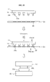
- FIG. 1 shows a view for explaining a conventional flip chip bonding.
- a flip chip bonding has a structure that, after forming a stud bump 13 on a bonding pad 12 of a chip 11 cut away from a wafer 10 and flipping the chip 11 , the bonding pad 12 of the chip 111 is directly bonded to a lead pad 22 of a substrate 21 .
- the flip chip bonding is classified into a package type flip chip bonding for bonding a flip chip in a ceramic package and a on-board type flip chip bonding for directly bonding a flip chip on a main board.
- FIG. 2 is a view showing an example of a package type flip chip bonding
- FIG. 3 is a view showing an example of an on-board type flip chip bonding.
- a chip 11 is bonded to a ceramic package 22 by a flip chip bonding method.
- the package is mounted on a main board 25 .
- the ceramic package 22 is sealed by a package cover 26 .
- the part that is connected by bumps 53 is molded by resin and the like.
- a conventional layer-built structure of a substrate consists of a basic substance, Cu, Ni, and Au.
- a surface treatment is performed to enhance an adhesive property.
- the surface treatment is conventionally performed by plating with Ni or Au.
- a substance 21 - 1 of the substrate is FPCB, FR4, FR5, ceramic, or glass. That is, after coating with a Cu layer 21 - 2 on the basic substance 21 - 1 , a pattern is formed. Then, a Ni layer 21 - 3 and an Au layer 21 - 4 are formed through an electroplating process to perform the surface treatment for enhancing an adhesion property.
- the invention has been made in view of the above problems, and it is an object of the invention to provide a flip chip bonding method for obtaining high reliability and productivity by speeding up process rate and for enhancing bonding performance.
- a flip chip bonding method comprising the steps of: performing pretreatment of a wafer having chips, dicing it, and obtaining the pretreated individual chip; performing pretreatment of a substrate; aligning the pads of the pretreated chip with the pads of the pretreated substrate, and bonding the chip and the substrate together by applying an ultrasonic wave and heat using a collet and simultaneously applying pressure; and performing post treatment for filling or molding resin after bonding.
- the bump of the substrate may have the same size as the bump of the chip or any one of the bump of the substrate and the bump of the chip may have a larger size than the other.
- the circuit part of the substrate may be plated with Sn. The flip chip bonding may be performed without damaging the pad of the chip, even though the wafer having a weak pad is used.
- a metal layer-built structure comprising: a substrate which is formed with a copper thin film pattern on a basic substance; a hard metal layer which is formed by plating a metal having a high hardness on the substrate; and a conductive metal layer which is formed by plating a metal having a high conductivity on the hard metal layer.
- FIGS. 1 to 3 are views for explaining a conventional flip chip bonding
- FIG. 4 is a view showing a layer-built structure of a conventional substrate for flip chip bonding
- FIG. 5 is a flow diagram showing a flip chip packaging process for enhancing a bonding property according to the invention.
- FIG. 6 is a view showing a process for forming a plated bump according to the invention.
- FIGS. 7 to 9 are views showing a method for giving an annealing effect to enhance an adhesion property of a plated bump according to the invention.
- FIG. 10 is a view showing a process for forming a doping bump on a substrate according to the invention.
- FIG. 11 is a view showing a process for forming a stud bump according to the invention.
- FIGS. 12 to 16 are views showing the examples of a stud bump according to the invention.
- FIG. 17 is a view showing a process for forming a wedge bump according to the invention.
- FIGS. 18 to 20 are views showing examples of a wedge bump according to the invention.
- FIG. 21 is a view showing an example of a tape adhesion process shown in FIG. 5 ;
- FIG. 22 is a view showing an example of a wafer cutting process shown in FIG. 5 ;
- FIG. 23 is a view showing an example of a flip chip bonding device developed according to the invention.
- FIGS. 24 to 27 are views showing examples of a design of a collet developed according to the invention.
- FIG. 28 is a view showing a coating method for minimizing the loss of an ultrasonic energy of a collet according to the invention.
- FIGS. 29 to 38 are views showing examples of a structure for bonding a substrate and a chip according to the invention.
- FIGS. 39 to 42 are views showing examples of a bonding structure according to the relative size of a stud bump or a wedge bump and examples of applying ACF, ACP, NCF or NCP after forming the bump;
- FIGS. 43 to 46 are views showing example of a chip stack method using a flip chip bonding process
- FIG. 47 is a view showing an example of a bonding post treatment process shown in FIG. 5 ;
- FIG. 48 is a view showing a first embodiment of a metal layer-built structure of a substrate for a flip chip bonding according to the invention.
- FIG. 49 is a view showing a second embodiment of a metal layer-built structure of a substrate for a flip chip bonding according to the invention.
- FIG. 5 is a flow diagram showing a flip chip packaging process according to the invention.
- a flip chip packaging method of the invention comprises bonding pretreatment steps for receiving a wafer and for performing a pretreatment for bonding on a bonding pad of the wafer (S 1 and S 2 ), a step for adhere a tape (S 3 ), a step for transferring the wafer (S 4 ), a step for performing a pretreatment for bonding on a lead pad of a substrate (S 5 and S 6 ), a step for bonding a flip chip by a thermosonic process (S 7 ), a bonding post treatment step (S 8 ), and inspecting step (S 9 ).
- the bonding pretreatment step S 2 for a wafer 10 may be any one selected from processes including forming a stud bump made of Au, Al, or Cu on an Aluminum pad 12 of the wafer 10 , forming a wedge bump with the same metal by wedge bonding, forming by evaporating a Au plated bump, Al, or Ag on an aluminum pad 12 , and forming a first plated bump and then forming a stud bump or a wedge bump, which is made of Au, Ag, Al, or Cu, on the first plated bump.
- the bonding pretreatment step S 9 for a substrate 21 may be any one selected from processes including forming a stud bump or a wedge bump, which is made of Au, Cu, or Al, on an aluminum pad 22 of the substrate 21 , forming an Au plated bump on an aluminum pad 22 , and applying Anisotropic Conductive Film (ACF), Anisotropic Conductive Paste (ACP), N on Conductive Film (NCF), and N on Conductive Paste (NCP) on the substrate.
- ACF Anisotropic Conductive Film
- ACP Anisotropic Conductive Paste
- NCF N on Conductive Film
- NCP N on Conductive Paste
- NCP N on Conductive Paste
- the substrate 21 to which a semiconductor chip 11 is bonded may be any one selected from ceramic, PCB, and FPCB.
- a method for a plated bump 32 on the wafer 10 or the substrate according to the invention comprises the steps of covering a protection film 31 except for the pad 12 or 22 in the wafer 10 or the substrate 21 , evaporating Au or Al or evaporating Ni and then evaporating Au on an upper surface thereof using a conventional plating method, such as an electrolytic plating or an electroless plating, and forming the plating bump 32 by removing the protection film 31 .
- a conventional plating method such as an electrolytic plating or an electroless plating
- the plated bump 32 formed on the wafer 10 or the substrate 21 is made of Au particles.
- an annealing effect may be applied to make a size of Au particles 36 large.
- FIG. 7 is a view showing a status for giving a n annealing effect on the formed plated bump by applying a heat
- FIG. 8 shows an example which gives an annealing effect by applying laser beam 37 to the plated bump 32
- FIG. 9 shows an example which gives an annealing effect by processing the plated bump 32 with a coming capillary 38 .
- FIG. 10 shows a method for forming a doping bump on a substrate according to the invention.
- a doping bump 53 may be formed by a doping method for partially projecting particles 46 of Au, Ag, or Cu on the substrate or the wafer and growing the particles.
- a pad 22 of the substrate that is plated with Au, Cu, Al, or Sn may be used.
- the stud bump 53 is formed on the pad 12 or 22 using a capillary 52 into which a gold wire 51 is inserted. Specifically, while applying are to the gold wire 51 and melting the gold wire 51 , the melted gold within the capillary 52 is contacted on a pad of the wafer 10 or the substrate 21 . Then, the melted gold is adhered to the pad by applying an ultrasonic wave. Then, the capillary 52 is moved a little in the direction of a transverse axis to flatten a projected portion. Then, the capillary 52 is moved upward. As a result, only the stud bump 53 is left behind on the pad.
- the stud bump 53 formed by the above method may have various shapes. That is, as shown if FIG. 12 , the stud bump 53 may have a body portion 53 - 1 and a long neck portion 53 - 2 formed in the center of the body portion 53 - 1 . Further, as shown in FIG. 13 , the stud bump 53 may have a short neck portion 53 - 2 formed on a body portion 53 - 1 . Further, as shown in FIG. 14 , the stud bump 53 may have a convex shape without having projection in the center of a body portion 53 - 1 . Further, as shown in FIG.
- the stud bump 53 may have a body portion 53 - 1 having a trapezoid shape without having the neck portion 53 - 2 in the center of the body portion. Further, as shown in FIG. 16 , the stud bump 53 may have a very thick body portion 53 - 1 without having the neck portion 53 - 2 . Since a noxious flux is not used in the stud bump forming process, the stud bump forming process is environmentally friendly and simple compared to a soldering method.
- the wedge bump 63 is formed on the pad 12 or 22 using a wedge bonding tool 65 into which a gold wire 61 or a high conductive wire that is made of Al, Cu, or Ag is inserted.
- a gold wire 61 or a high conductive wire that is made of Al, Cu, or Ag is inserted.
- the wedge bonding tool 65 is moved a little in the direction of a transverse axis to adhere each wire.
- each wire is immediately cut.
- the wedge bump 63 is formed on the wafer 10 or the substrate 21 .
- the wedge bump 63 formed by the above method has various shapes. That is, FIGS. 18 to 20 show the wedge bumps 63 having two projections, one projection and no projection, respectively.
- the shape of the wedge bump 63 depends on the shapes of various wedge tools.
- a die that is, a chip
- the tape 72 is supported by a frame ring 74 positioned at both ends thereof, the wafer 10 is placed on an adhesive surface of the tape and then adhered to it.
- a chip of a wafer status is individually separated by a cutter. According to a sectional side elevation shown in FIG. 22 , even if a blade 81 of a cutter 80 completely cuts a wafer 10 and partially cuts a tape 72 , chip 11 is not individually separated by the tape 72 .
- FIG. 23 is a schematic view showing a bonding device upon bonding a flip chip according to the invention.
- the bonding device comprises a collet 95 for holding a chip 11 , and a block 100 for supporting a substrate 21 .
- the collet 95 holding the chip 11 may vibrate in the direction of an X axis, and the block 100 supporting the substrate 21 may vibrate in the direction of a Y axis. Further, the collet 95 may vibrate in the direction of the Y axis, and the block 100 may vibrate in the direction of the X axis. Further, the collet 95 and the block 100 may transfer the ultrasonic waves while intersecting in the direction of the same axis.
- Each of the above transmission methods may be used together with a conventional method that transfers the ultrasonic wave only from the collet 95 .
- the ultrasonic waves may be transferred to the substrate 21 as well as the chip 11 , a flip chip bonding process is completed in a short time, and an adhesion strength between the chip 11 and the substrate 21 is increased. As a result, a production yield is enhanced.
- the collet 95 transferring the ultrasonic energy to the chip is formed with a vacuum hole 96 in the center thereof, it serves to hold the chip 11 using a vacuum pressure and to transfer the ultrasonic energy.
- the above collet 95 is classified into a polish type that polishes a contact surface as shown in FIG. 26 , and a matt type that roughly treats a contact surface as shown in FIG. 27 .
- the collet is manufactured using a material for enduring ultrasonic waves, such as Zr, Ti, ceramic, stainless alloy, titanium alloy, for example, TiW or TiC, and the like.
- the collet 95 may be treated by diamond like carbon (DLC) coating to prevent the loss of the ultrasonic energy.
- DLC diamond like carbon
- the DLC coating is made by growing a carbon atom 98 on the surface of the collet 95 using sputtering 99 or CVD (chemical vapor deposition) and forming a diamond layer. If the diamond like carbon thin film 97 is coated on the outer surface of the collet, the outside loss of ultrasonic energy transferred from a transducer is minimized, and, thus, the ultrasonic energy is efficiently transferred to the chip.
- a bonding structure of the invention for flip chip bonding when a chip 11 is bonded on a pretreated substrate 21 has various structures as described in the following Table 1 according to the method for forming a bump on a pad 22 of the substrate and a pad 12 of the chip.
- Example 1 (FIG. 29) Stud bump is formed Plated bump is formed Example 2 (FIG. 30) Bare Plated bump is formed Example 3 (FIG. 31) Stud bump is formed Plated bump and stud bump are formed Example 4 (FIG. 32) Bare Plated bump and stud bump are formed Example 5 (FIG. 33) Stud bump is formed Stud bump is formed Example 6 (FIG. 34) Stud bump is formed Bare Example 7 (FIG. 35) Bare Stud bump is formed Example 8 (FIG. 36) Bare + Adhesive Stud bump is formed (ACF, ACP, NCF, or NCP) application Example 9 (FIG. 37) Bare + Adhesive Plated bump is formed (ACF, ACP, NCF, or NCP) application Example 10 (FIG. 38) Plated bump is formed Plated bump is formed or not.
- FIG. 29 is a view showing the process for a flip chip bonding between a substrate that is formed with a stud bump and a chip that is formed with a plated bump using a thermosonic method according to the invention.
- an aluminum bonding pad 12 of a chip 11 is formed with a plated bump 32 c that is made of Au, Al, or Ni coated with Au.
- a lead pad 22 of a substrate 21 is formed with a stud bump 53 s that is made of Au or Cu.
- the plated bump 32 c of the chip and the stud bump 53 s of the substrate are bonded by energy generated from the heat, the ultrasonic wave and the pressure.
- the collet 95 that is made of Zr, Ti, ceramic, stainless alloy, TiW alloy, TiC, and the like, is manufactured to have a little smaller size than that of each chip.
- FIG. 30 is a view showing the process for a flip chip bonding between a bare substrate and a chip that is formed with a plated bump u sing a thermosonic method according to the invention.
- an aluminum bonding pad 12 of a chip 11 is formed with a plated bump 32 c that is made of Au, Al, or Ni coated with Au.
- a lead pad 22 of a substrate 21 is bare of any bump.
- heat is applied to the substrate 21 , and an ultrasonic wave is applied to the chip 11 through a collet 95 .
- pressure is applied to the substrate 21 .
- the plated bump 32 c of the chip and the lead pad 22 of the substrate are bonded by energy generated from the heat, the ultrasonic wave and the pressure.
- FIG. 31 is a view showing the process for a flip chip bonding between a substrate that is formed with a stud bump and a chip that is formed with a plated bump and a stud bump formed on the plated bump using a thermosonic method according to the invention.
- an aluminum bonding pad 12 of a chip 11 is formed with a plated bump 32 c that is made of Au, Al, Ag, Cu or Ni coated with Au.
- a stud bump 53 c is again formed on the plated bump 32 c .
- a lead pad 22 of a substrate 21 is formed with a stud bump 53 s .
- the flip chip bonding process S 5 after the chip 11 and the substrate 21 are closely contacted, heat is applied to the substrate 21 , and an ultrasonic wave of 70 KHz or more is applied to the chip 11 through a collet 95 . Simultaneously, pressure is applied to the substrate 21 .
- the stud bump 53 c of the chip 11 and the stud bump 53 s of the substrate are bonded by energy generated from the heat, the ultrasonic wave of 70 KHz or more and the pressure.
- FIG. 32 is a view showing the process for a flip chip bonding between a base substrate and a chip that is formed with a plated bump and a stud bump formed on the plated bump using a thermosonic method according to the invention.
- an aluminum bonding pad 12 of a chip 11 is formed with a plated bump 32 c that is made of Au, Al, or Ni coated with Au.
- a stud bump 53 c is again formed on the plated bump 32 c .
- a lead pad 22 of a substrate 21 is bare of any bump.
- heat is applied to the substrate 21 , and an ultrasonic wave is applied to the chip 11 through a collet 95 . Simultaneously, pressure is applied to the substrate 21 .
- the stud bump 53 c of the chip and the lead pad 22 of the substrate are bonded by energy generated from the heat, the ultrasonic wave of 70 KHz or more and the pressure.
- FIG. 33 is a view showing the process for a flip chip bonding between a substrate that is formed with a stud bump 53 s and a chip that is formed with a stud bump 53 c using a thermosonic method according to the invention.
- an aluminum bonding pad 12 of a chip 11 is formed with a stud bump 53 c that is made of Au or Cu.
- a lead pad 22 of a substrate 21 is formed with a stud bump 53 s that is made of Au or Cu.
- heat is applied to the substrate 21 , and an ultrasonic wave is applied to the chip 11 through a collet 95 .
- pressure is applied to the substrate 21 .
- the stud bump 53 c of the chip and the stud bump 53 s of the substrate are bonded by energy generated from the heat, the ultrasonic wave and the pressure.
- FIG. 34 is a view showing the process for a flip chip bonding between a substrate that is formed with a stud bump 53 s and a chip that is formed with a basic aluminum pad using a thermosonic method according to the invention.
- an aluminum bonding pad 12 of a chip 11 is bare of any bump.
- a lead pad 22 of a substrate 21 is formed with a stud bump 53 s that is made of Au or Cu.
- heat is applied to the substrate 21 , and an ultrasonic wave is applied to the chip 11 through a collet 95 .
- pressure is applied to the substrate 21 .
- the bonding pad 12 of the chip and the stud bump 53 s of the substrate are bonded by energy generated from the heat, the ultrasonic wave and the pressure.
- FIG. 35 is a view showing the process for a flip chip bonding between a base substrate and a chip that is formed with a stud bump 53 c using a thermosonic method according to the invention.
- an aluminum bonding pad 12 of a chip 11 is formed with a stud bump 53 c that is made of Au or Cu.
- a lead pad 22 of a substrate 21 is bare of any bump.
- heat is applied to the substrate 21
- an ultrasonic wave is applied to the chip 11 through a collet 95 .
- pressure is applied to the substrate 21 .
- the stud bump 53 c of the chip and the lead pad 22 of the substrate 21 are bonded by energy generated from the heat, the ultrasonic wave and the pressure.
- FIG. 36 is a view showing the process for a flip chip bonding between a base substrate on which an adhesive (for example, ACF, ACP, NCF or NCP) is applied and a chip that is formed with a stud bump 53 c using a thermosonic method according to the invention.
- an adhesive for example, ACF, ACP, NCF or NCP
- an aluminum bonding pad 12 of a chip 11 is formed with a stud bump 53 c that is made of Au or Cu.
- a lead pad 22 of a substrate 21 is bare of any bump.
- An adhesive 102 that is selected from a group of Anisotropic Conductive Film (ACF), Anisotropic Conductive Paste (ACP), N on Conductive Film (NCF), and N on Conductive Paste (NCP) is applied on the lead pad 22 of the substrate 21 .
- ACF Anisotropic Conductive Film
- ACP Anisotropic Conductive Paste
- NCF N on Conductive Film
- NCP N on Conductive Paste
- FIG. 37 is a view showing the process for a flip chip bonding between a base substrate on which an adhesive (ACF, ACP, NCF or NCP) is applied and a chip that is formed with a plated bump using a thermosonic method according to the invention.
- an aluminum bonding pad 12 of a chip 11 is formed with a plated bump 32 c that is made of Au, Al, or Ni coated with Au.
- a lead pad 22 of a substrate 21 is bare of any bump.
- An adhesive 102 that is selected from ACF, ACP, NCF, and NCP is applied on the lead pad 22 of the substrate 21 .
- heat is applied to the substrate 21
- ultrasonic wave is applied to the chip 11 through a collet 95 .
- pressure is applied to the substrate 21 .
- the plated bump 32 c of the chip and the lead pad 22 of the substrate 21 are bonded by energy generated from the heat, the ultrasonic wave and the pressure.
- the bump formed on the substrate 21 or the chip 11 according to the invention comprises a plated bump that is made of Au or Al, a plated bump that is made of Ni coated with Au, a stud bump that is made of Au, a stud bump that is made of Cu and the like.
- the substrate 21 may be a conventional PCB or FPCB.
- the substrate 21 may be a substrate on which Sn is plated. In order to perform a flip chip process for having better adhesion force, ACF, ACP, NCF or NCP is applied on the substrate.
- a chip 11 may have an aluminum pad 12 that is formed with a plated bump 32 c made of Au, Al or Ni coated with Au. Further, the chip 11 may have only the aluminum bonding pad 12 without forming the plated bump 32 c .
- a substrate 21 may be formed with a doping bump 43 . The chip 11 and the substrate 21 are bonded using an ultrasonic energy.
- the invention has an advantage in that, since the present invention adopts a method for applying the ultrasonic wave as well as a thermocompression method without using only a conventional thermocompression method, a process time may be reduced compared to the conventional art. Further, in the case of using a substrate on which Sn is plated, or a substrate on which ACF, ACP, NCF or NCP is applied, a superior adhesion force may be obtained.
- FIGS. 39 to 42 shows the examples of the bonding structure according to a relative size of a stud bump or a wedge bump and the example of applying ACF, ACP, NCF or NCP after forming a bump.
- a bump 53 c or 63 c of a chip 11 is larger than a bump 53 s or 63 s of a substrate 21 .
- a bump 53 c or 63 c has the same size as a bump 53 s or 63 s of a substrate 21 .
- a bump 53 s or 63 s of a substrate is larger than a bump 53 c or 63 c of a chip. From the foregoing, the bump 53 c or 63 c of the chip and the bump 53 s or 63 s of the substrate may be bonded while having the same size and kind or differing the size and kind thereof.
- an anisotropic conductive adhesive 102 or a nonconductive adhesive 102 such as ACF, ACP, NCF, NCP, and the like is applied, and then a chip 11 and the substrate 21 are immediately bonded.
- the process for filling resin may be removed.
- the process for applying the anisotropic conductive adhesive 102 or the nonconductive adhesive 102 such as ACF, ACP, NCF, NCP, and the like may be performed around the bump which is formed on the substrate 21 . Further, the process may be performed around the entire substrate 21 .
- a stud bump 53 or a wedge bump 63 is formed on a pad 12 of an upper chip 11 or a pad 12 of a lower chip 11 .
- the pad 12 of the lower chip has at least two rows.
- the pads of two chips 11 are positioned to face each other. Heat is applied to the lower chip 11 , and ultrasonic wave and force are applied through a collet 95 to the upper chip 11 .
- the upper chip 11 and the lower chip 11 are bonded to form a stacked chip. This stacked chip shows better performance than one chip.
- FIG. 44 shows a view for manufacturing a stacked chip according to the invention by forming a stud bump 53 or a wedge bump 63 on an upper chip 11 , forming a stud bump 53 or a wedge bump 63 on a lower chip 11 , facing them to each other, and applying ultrasonic waves and force using a tool.
- FIG. 45 shows a view for manufacturing a stacked chip according to the invention by forming a plated bump 32 on an upper chip 11 , forming a stud bump 53 or a wedge bump 63 on a lower chip 11 , and bonding them.
- FIG. 46 shows a view for manufacturing a stacked chip according to the invention by forming a plated bump 32 on an upper chip 11 , and bonding this chip 11 to a lower chip 11 .
- the bump adopted in the chip-to-chip method as describe above is made by forming a wire with a metal having a good conductivity, such as Au, Ag, Al, and Cu.
- FIG. 47 shows an example of forming a protection wall 132 , forming bumps 53 c , 53 s and 63 on a chip 11 and a substrate 21 , respectively, and forming a molding 134 on them. Specifically, if, in the pretreatment process, the protection wall 132 is formed around the chip and then a flip chip bonding is performed in a post treatment for under-fill and side sealing, an epoxy resin component is prevented from penetrating into a gap between the bump and the substrate.
- the protection wall 132 may be made of NCP, NCF, ACF, ACP, epoxy, or a molding compound. After performing a flip chip bonding process, it is preferred that a curing process for hardening the protection wall 132 which is made of a soft material is added.
- a layer-built structure of a substrate for bonding comprises a substrate which is formed with a copper thin film pattern on a basic substance, a hard metal layer which is formed by plating a metal having a high hardness on the substrate, a conductive metal layer which is formed by plating a metal having a high conductivity on the hard metal layer.
- FIG. 48 shows an example of a metal layer-built structure of a substrate for a stud bump according to the invention.
- a substrate 21 according to the invention is formed with a copper thin film pattern on a basic substance thereof.
- the basic substance of the substrate is made of FPCB, FR4, FR5, ceramic or glass.
- a first metal layer 141 and a second metal layer 142 are formed on the substrate 21 by a plating method.
- the first metal layer 141 serves as a buffer layer for cutting off the effect according to the kind of the substance of the substrate. It is formed by plating Pd alloy, Pd—Ni or Ni—Pd to have 3 microns or more in thickness.
- the second metal layer 142 serves as a part for directly connecting to a stud bump or the like in a bonding process. It is formed by plating Au or Ag having a good conductivity and purity, Au/Ag, Al, Au alloy, Ag alloy or Al alloy to have 0.1 microns or more in thickness.
- the buffer layer 141 of the hard metal for cutting off the effect according to the kind of the substrate is added, a bonding strength is maintained and a production yield is enhanced irrespective of the kind of the basic substance.
- FIG. 49 shows a layer-built structure having three layers as another embodiment of a metal layer-built structure of a substrate for each bump according to the invention.
- a substrate 21 according to the invention is formed with a copper thin film pattern on a basic substance thereof.
- the basic substance of the substrate is made of FPCB, FR4, FR5, ceramic or glass.
- a first metal layer 141 , a second metal layer 142 and a third metal layer 143 are formed on the substrate 21 by a plating method.
- the first metal layer 151 is formed by plating Ni or Ni alloy to have 3 microns or more in thickness.
- the second metal layer 152 serves as a buffer layer for cutting off the effect according to the kind of the substance of the substrate. It is formed by plating AU alloy to have 0.1 microns or more in thickness.
- the third metal layer 153 serves as a part for directly connecting to each bump or the like in a bonding process. It uses Au or Ag having a good conductivity and purity, Al, Au alloy, Ag alloy or Al alloy.
- the buffer layer of the hard metal for cutting off the effect according to the kind of the substrate is added, a bonding strength is maintained and a production yield is enhanced irrespective of the kind of the basic substance.
- a bonding property of a chip may be greatly enhanced by forming a stud bump or a plated bump on the chip, forming a bump on a substrate, and directly bonding the bumps. That is, the invention may enhance the bonding property by directly connecting the plated bump, a stud bump, a wedge bump or a doping bump using a collet and forming a new intermetallic area after bonding. Further, since a substrate plated with Al, Cu or Sn having a lower melting point than Au, electrical reliability is easily secured and adhesion force is superior. Thus, the flip chip bonding can be accomplished without damaging a chip pad even though a wafer having a weak pad, such as an image sensor and the like, is used.
Landscapes
- Engineering & Computer Science (AREA)
- Computer Hardware Design (AREA)
- Microelectronics & Electronic Packaging (AREA)
- Power Engineering (AREA)
- Manufacturing & Machinery (AREA)
- Physics & Mathematics (AREA)
- Condensed Matter Physics & Semiconductors (AREA)
- General Physics & Mathematics (AREA)
- Wire Bonding (AREA)
Applications Claiming Priority (2)
| Application Number | Priority Date | Filing Date | Title |
|---|---|---|---|
| KR20030083891 | 2003-11-25 | ||
| KR2003-0083891 | 2003-11-25 |
Publications (2)
| Publication Number | Publication Date |
|---|---|
| US20050110163A1 US20050110163A1 (en) | 2005-05-26 |
| US7115446B2 true US7115446B2 (en) | 2006-10-03 |
Family
ID=34588038
Family Applications (1)
| Application Number | Title | Priority Date | Filing Date |
|---|---|---|---|
| US10/964,371 Expired - Fee Related US7115446B2 (en) | 2003-11-25 | 2004-10-13 | Flip chip bonding method for enhancing adhesion force in flip chip packaging process and metal layer-built structure of substrate for the same |
Country Status (7)
Cited By (21)
| Publication number | Priority date | Publication date | Assignee | Title |
|---|---|---|---|---|
| US20060211233A1 (en) * | 2005-03-21 | 2006-09-21 | Skyworks Solutions, Inc. | Method for fabricating a wafer level package having through wafer vias for external package connectivity and related structure |
| US20070108627A1 (en) * | 2005-11-15 | 2007-05-17 | Matsushita Electric Industrial Co., Ltd. | Semiconductor device and method for manufacturing the same |
| US20070222087A1 (en) * | 2006-03-27 | 2007-09-27 | Sangdo Lee | Semiconductor device with solderable loop contacts |
| US20080003761A1 (en) * | 2005-04-01 | 2008-01-03 | Skyworks Solutions, Inc. | Method for fabricating a wafer level package with device wafer and passive component integration |
| US20090014852A1 (en) * | 2007-07-11 | 2009-01-15 | Hsin-Hui Lee | Flip-Chip Packaging with Stud Bumps |
| US20090033840A1 (en) * | 2007-07-31 | 2009-02-05 | Chunghwa Picture Tubes, Ltd. | Chip module, active device array substrate and liquid crystal display panel |
| US20090051016A1 (en) * | 2007-08-20 | 2009-02-26 | Ivan Galesic | Electronic component with buffer layer |
| US20090155955A1 (en) * | 2007-12-17 | 2009-06-18 | Steve Xin Liang | Thermal mechanical flip chip die bonding |
| WO2009085409A1 (en) * | 2007-12-26 | 2009-07-09 | Skyworks Solutions, Inc. | In-situ cavity integrated circuit package |
| US20100007010A1 (en) * | 2008-07-11 | 2010-01-14 | Advanced Semiconductor Engineering, Inc. | Semiconductor package, method for enhancing the bond of a bonding wire, and method for manufacturing a semiconductor package |
| WO2010055970A1 (ko) * | 2008-11-12 | 2010-05-20 | 한국과학기술원 | 접착제의 발열 온도 조절을 통한 전자부품간 접속 방법 및 접착제의 발열 온도 조절을 통한 전자부품간 접속 장치 |
| US20100244161A1 (en) * | 2007-11-30 | 2010-09-30 | Skyworks Solutions, Inc. | Wafer level packaging using flip chip mounting |
| US20130087915A1 (en) * | 2011-10-10 | 2013-04-11 | Conexant Systems, Inc. | Copper Stud Bump Wafer Level Package |
| US8618795B1 (en) * | 2012-06-29 | 2013-12-31 | General Electric Company | Sensor assembly for use in medical position and orientation tracking |
| US9209147B1 (en) | 2014-07-17 | 2015-12-08 | Freescale Semiconductor, Inc. | Method of forming pillar bump |
| US9397137B2 (en) | 2012-07-11 | 2016-07-19 | Taiwan Semiconductor Manufacturing Company, Ltd. | Interconnect structure for CIS flip-chip bonding and methods for forming the same |
| US20160225800A1 (en) * | 2015-01-30 | 2016-08-04 | Boe Technology Group Co., Ltd. | Method and system of flattening a surface formed by sealant of packaging cover plate, and packaging method |
| US9683278B2 (en) | 2015-06-08 | 2017-06-20 | Infineon Technologies Ag | Diffusion solder bonding using solder preforms |
| US9840785B2 (en) | 2014-04-28 | 2017-12-12 | Samsung Electronics Co., Ltd. | Tin plating solution, tin plating equipment, and method for fabricating semiconductor device using the tin plating solution |
| US20180114772A1 (en) * | 2016-10-24 | 2018-04-26 | Palo Alto Research Center Incorporated | Method for simultaneously bonding multiple chips of different heights on flexible substrates using anisotropic conductive film or paste |
| US12040260B2 (en) | 2020-12-31 | 2024-07-16 | Texas Instruments Incorporated | Electronic package with surface contact wire extensions |
Families Citing this family (29)
| Publication number | Priority date | Publication date | Assignee | Title |
|---|---|---|---|---|
| US7142909B2 (en) * | 2002-04-11 | 2006-11-28 | Second Sight Medical Products, Inc. | Biocompatible bonding method and electronics package suitable for implantation |
| US7348212B2 (en) * | 2005-09-13 | 2008-03-25 | Philips Lumileds Lighting Company Llc | Interconnects for semiconductor light emitting devices |
| US8225499B2 (en) * | 2005-06-16 | 2012-07-24 | Imbera Electronics Oy | Method for manufacturing a circuit board structure, and a circuit board structure |
| JP4768343B2 (ja) * | 2005-07-27 | 2011-09-07 | 株式会社デンソー | 半導体素子の実装方法 |
| US7408243B2 (en) * | 2005-12-14 | 2008-08-05 | Honeywell International Inc. | High temperature package flip-chip bonding to ceramic |
| US20070141749A1 (en) * | 2005-12-20 | 2007-06-21 | Yi-Fong Lin | Die attachment method for LED chip and structure thereof |
| JP4552916B2 (ja) * | 2005-12-21 | 2010-09-29 | 株式会社大真空 | 圧電振動デバイス |
| JP4863746B2 (ja) | 2006-03-27 | 2012-01-25 | 富士通株式会社 | 半導体装置およびその製造方法 |
| KR100762909B1 (ko) * | 2006-08-31 | 2007-10-08 | 주식회사 하이닉스반도체 | 플립 칩 패키지의 제조 방법 |
| US8258625B2 (en) * | 2007-04-06 | 2012-09-04 | Hitachi, Ltd. | Semiconductor device |
| KR100896127B1 (ko) * | 2007-07-20 | 2009-05-07 | 성균관대학교산학협력단 | 솔더가 코팅된 전해 도금 범프 및 이를 사용하는 플립칩접합 방법 |
| US7749887B2 (en) | 2007-12-18 | 2010-07-06 | Micron Technology, Inc. | Methods of fluxless micro-piercing of solder balls, and resulting devices |
| DE102008040614A1 (de) | 2008-07-22 | 2010-01-28 | Robert Bosch Gmbh | Kontaktierungsverfahren für substratbasierte Schaltungen und zugehörige Schaltungsanordnung |
| KR100958513B1 (ko) | 2008-07-31 | 2010-05-17 | 알티전자 주식회사 | 전극 패드 및 그 전극 패드를 포함하는 발광 다이오드패키지 |
| WO2010033107A1 (en) * | 2008-09-16 | 2010-03-25 | Agere Systems, Inc. | Pb-free solder bumps with improved mechanical properties |
| TWI404198B (zh) * | 2009-04-22 | 2013-08-01 | Ind Tech Res Inst | 感測器之封裝結構與封裝方法 |
| US8476757B2 (en) * | 2009-10-02 | 2013-07-02 | Northrop Grumman Systems Corporation | Flip chip interconnect method and design for GaAs MMIC applications |
| JP2011151322A (ja) * | 2010-01-25 | 2011-08-04 | Japan Aviation Electronics Industry Ltd | フリップチップ実装構造及びフリップチップ実装方法 |
| TWI411075B (zh) * | 2010-03-22 | 2013-10-01 | Advanced Semiconductor Eng | 半導體封裝件及其製造方法 |
| US9406658B2 (en) | 2010-12-17 | 2016-08-02 | Advanced Semiconductor Engineering, Inc. | Embedded component device and manufacturing methods thereof |
| TW201243930A (en) * | 2011-04-21 | 2012-11-01 | Lingsen Precision Ind Ltd | Wafer dicing method |
| KR102380834B1 (ko) | 2015-01-06 | 2022-03-31 | 삼성전기주식회사 | 인쇄회로기판, 반도체 패키지 및 이들의 제조방법 |
| KR20160095520A (ko) | 2015-02-03 | 2016-08-11 | 삼성전기주식회사 | 인쇄회로기판, 반도체 패키지 및 이들의 제조방법 |
| JP2016001752A (ja) * | 2015-08-25 | 2016-01-07 | 日本航空電子工業株式会社 | フリップチップ実装構造、フリップチップ実装方法及びフリップチップ実装構造の使用方法 |
| KR101880102B1 (ko) * | 2017-05-30 | 2018-07-20 | 제엠제코(주) | 적층식 반도체 패키지 |
| US11495524B2 (en) * | 2018-06-12 | 2022-11-08 | Texas Instruments Incorporated | QFN device having a mechanism that enables an inspectable solder joint when attached to a PWB and method of making same |
| US11862587B2 (en) * | 2019-07-25 | 2024-01-02 | Advanced Semiconductor Engineering, Inc. | Semiconductor package structure and method of manufacturing the same |
| JP7257296B2 (ja) * | 2019-09-06 | 2023-04-13 | ファスフォードテクノロジ株式会社 | ダイボンディング装置および半導体装置の製造方法 |
| CN111009481B (zh) * | 2019-12-19 | 2023-04-18 | 西北电子装备技术研究所(中国电子科技集团公司第二研究所) | 芯片基板大压力倒装键合柔性加压方法 |
Citations (4)
| Publication number | Priority date | Publication date | Assignee | Title |
|---|---|---|---|---|
| US20010029088A1 (en) * | 1999-03-03 | 2001-10-11 | Hitoshi Odajima | Method and apparatus for separating semiconductor elements, and mounting method of semiconductor elements |
| US20020133943A1 (en) * | 2001-03-22 | 2002-09-26 | Noriaki Sakamoto | Method for manufacturing circuit device |
| US6576499B2 (en) * | 1999-12-10 | 2003-06-10 | Nec Corporation | Electronic device assembly and a method of connecting electronic devices constituting the same |
| US6888230B1 (en) * | 1998-10-28 | 2005-05-03 | Renesas Technology Corp. | Semiconductor device, semiconductor wafer, semiconductor module, and a method of manufacturing semiconductor device |
Family Cites Families (12)
| Publication number | Priority date | Publication date | Assignee | Title |
|---|---|---|---|---|
| JPH07115109A (ja) * | 1993-10-15 | 1995-05-02 | Nec Corp | フリップチップボンディング方法及び装置 |
| US5503286A (en) * | 1994-06-28 | 1996-04-02 | International Business Machines Corporation | Electroplated solder terminal |
| JP3243956B2 (ja) * | 1995-02-03 | 2002-01-07 | 松下電器産業株式会社 | 半導体装置およびその製造方法 |
| JPH1012669A (ja) * | 1996-06-21 | 1998-01-16 | Toshiba Corp | フリップチップの接続方法 |
| JPH10209218A (ja) * | 1997-01-24 | 1998-08-07 | Rohm Co Ltd | 異方性導電膜を有する半導体チップの製造方法、およびこの半導体チップの実装方法 |
| JP3923248B2 (ja) * | 1996-12-27 | 2007-05-30 | 松下電器産業株式会社 | 回路基板への電子部品の実装方法及び回路基板 |
| US5950070A (en) * | 1997-05-15 | 1999-09-07 | Kulicke & Soffa Investments | Method of forming a chip scale package, and a tool used in forming the chip scale package |
| JPH11284028A (ja) * | 1998-03-27 | 1999-10-15 | Toshiba Corp | ボンディング方法及びその装置 |
| KR20000002962A (ko) * | 1998-06-24 | 2000-01-15 | 윤종용 | 웨이퍼레벨의 칩스케일 패키지 및 그 제조방법 |
| JP2002151551A (ja) * | 2000-11-10 | 2002-05-24 | Hitachi Ltd | フリップチップ実装構造、その実装構造を有する半導体装置及び実装方法 |
| JP2003197672A (ja) * | 2001-12-25 | 2003-07-11 | Nec Electronics Corp | 半導体装置の製造方法 |
| KR100544274B1 (ko) * | 2003-06-25 | 2006-01-24 | (주)케이나인 | 스터드 범프용 기판의 금속 적층구조 |
-
2004
- 2004-05-28 KR KR1020040038214A patent/KR100604334B1/ko not_active Expired - Fee Related
- 2004-08-04 WO PCT/KR2004/001956 patent/WO2005053013A1/en active Application Filing
- 2004-09-02 SG SG200404949A patent/SG128468A1/en unknown
- 2004-09-21 TW TW093128559A patent/TWI255019B/zh not_active IP Right Cessation
- 2004-09-29 CN CNA2004100803660A patent/CN1622304A/zh active Pending
- 2004-10-13 US US10/964,371 patent/US7115446B2/en not_active Expired - Fee Related
- 2004-11-19 JP JP2004336518A patent/JP2005159356A/ja active Pending
Patent Citations (4)
| Publication number | Priority date | Publication date | Assignee | Title |
|---|---|---|---|---|
| US6888230B1 (en) * | 1998-10-28 | 2005-05-03 | Renesas Technology Corp. | Semiconductor device, semiconductor wafer, semiconductor module, and a method of manufacturing semiconductor device |
| US20010029088A1 (en) * | 1999-03-03 | 2001-10-11 | Hitoshi Odajima | Method and apparatus for separating semiconductor elements, and mounting method of semiconductor elements |
| US6576499B2 (en) * | 1999-12-10 | 2003-06-10 | Nec Corporation | Electronic device assembly and a method of connecting electronic devices constituting the same |
| US20020133943A1 (en) * | 2001-03-22 | 2002-09-26 | Noriaki Sakamoto | Method for manufacturing circuit device |
Cited By (40)
| Publication number | Priority date | Publication date | Assignee | Title |
|---|---|---|---|---|
| US20060211233A1 (en) * | 2005-03-21 | 2006-09-21 | Skyworks Solutions, Inc. | Method for fabricating a wafer level package having through wafer vias for external package connectivity and related structure |
| US20080064142A1 (en) * | 2005-03-21 | 2008-03-13 | Skyworks Solutions, Inc. | Method for fabricating a wafer level package having through wafer vias for external package connectivity |
| US20080003761A1 (en) * | 2005-04-01 | 2008-01-03 | Skyworks Solutions, Inc. | Method for fabricating a wafer level package with device wafer and passive component integration |
| US7629201B2 (en) | 2005-04-01 | 2009-12-08 | Skyworks Solutions, Inc. | Method for fabricating a wafer level package with device wafer and passive component integration |
| US20070108627A1 (en) * | 2005-11-15 | 2007-05-17 | Matsushita Electric Industrial Co., Ltd. | Semiconductor device and method for manufacturing the same |
| US7629687B2 (en) * | 2005-11-15 | 2009-12-08 | Panasonic Corporation | Semiconductor device and method for manufacturing the same |
| US20070222087A1 (en) * | 2006-03-27 | 2007-09-27 | Sangdo Lee | Semiconductor device with solderable loop contacts |
| US20090014852A1 (en) * | 2007-07-11 | 2009-01-15 | Hsin-Hui Lee | Flip-Chip Packaging with Stud Bumps |
| US20090033840A1 (en) * | 2007-07-31 | 2009-02-05 | Chunghwa Picture Tubes, Ltd. | Chip module, active device array substrate and liquid crystal display panel |
| US20090051016A1 (en) * | 2007-08-20 | 2009-02-26 | Ivan Galesic | Electronic component with buffer layer |
| US8283756B2 (en) * | 2007-08-20 | 2012-10-09 | Infineon Technologies Ag | Electronic component with buffer layer |
| US8324728B2 (en) | 2007-11-30 | 2012-12-04 | Skyworks Solutions, Inc. | Wafer level packaging using flip chip mounting |
| US8809116B2 (en) | 2007-11-30 | 2014-08-19 | Skyworks Solutions, Inc. | Method for wafer level packaging of electronic devices |
| US20100244161A1 (en) * | 2007-11-30 | 2010-09-30 | Skyworks Solutions, Inc. | Wafer level packaging using flip chip mounting |
| WO2009079114A3 (en) * | 2007-12-17 | 2009-08-13 | Skyworks Solutions Inc | Thermal mechanical flip chip die bonding |
| US7642135B2 (en) | 2007-12-17 | 2010-01-05 | Skyworks Solutions, Inc. | Thermal mechanical flip chip die bonding |
| US20090155955A1 (en) * | 2007-12-17 | 2009-06-18 | Steve Xin Liang | Thermal mechanical flip chip die bonding |
| US8900931B2 (en) * | 2007-12-26 | 2014-12-02 | Skyworks Solutions, Inc. | In-situ cavity integrated circuit package |
| CN101978483B (zh) * | 2007-12-26 | 2014-07-16 | 斯盖沃克斯解决方案公司 | 原位空腔集成电路块 |
| KR20100119858A (ko) * | 2007-12-26 | 2010-11-11 | 스카이워크스 솔루션즈 인코포레이티드 | 인시튜 캐비티 집적 회로 패키지 |
| US20100283144A1 (en) * | 2007-12-26 | 2010-11-11 | Steve Xin Liang | In-situ cavity circuit package |
| WO2009085409A1 (en) * | 2007-12-26 | 2009-07-09 | Skyworks Solutions, Inc. | In-situ cavity integrated circuit package |
| US20150061125A1 (en) * | 2007-12-26 | 2015-03-05 | Skyworks Solutions, Inc. | Integrated circuit package including in-situ formed cavity |
| EP2235747A4 (en) * | 2007-12-26 | 2013-07-03 | Skyworks Solutions Inc | In-situ cavity integrated circuit package |
| US9153551B2 (en) * | 2007-12-26 | 2015-10-06 | Skyworks Solutions, Inc. | Integrated circuit package including in-situ formed cavity |
| US20100007010A1 (en) * | 2008-07-11 | 2010-01-14 | Advanced Semiconductor Engineering, Inc. | Semiconductor package, method for enhancing the bond of a bonding wire, and method for manufacturing a semiconductor package |
| US8018075B2 (en) | 2008-07-11 | 2011-09-13 | Advanced Semiconductor Engineering, Inc. | Semiconductor package, method for enhancing the bond of a bonding wire, and method for manufacturing a semiconductor package |
| WO2010055970A1 (ko) * | 2008-11-12 | 2010-05-20 | 한국과학기술원 | 접착제의 발열 온도 조절을 통한 전자부품간 접속 방법 및 접착제의 발열 온도 조절을 통한 전자부품간 접속 장치 |
| US20130087915A1 (en) * | 2011-10-10 | 2013-04-11 | Conexant Systems, Inc. | Copper Stud Bump Wafer Level Package |
| US8618795B1 (en) * | 2012-06-29 | 2013-12-31 | General Electric Company | Sensor assembly for use in medical position and orientation tracking |
| US9397137B2 (en) | 2012-07-11 | 2016-07-19 | Taiwan Semiconductor Manufacturing Company, Ltd. | Interconnect structure for CIS flip-chip bonding and methods for forming the same |
| US10090345B2 (en) | 2012-07-11 | 2018-10-02 | Taiwan Semiconductor Manufacturing Company, Ltd. | Interconnect structure for CIS flip-chip bonding and methods for forming the same |
| US9840785B2 (en) | 2014-04-28 | 2017-12-12 | Samsung Electronics Co., Ltd. | Tin plating solution, tin plating equipment, and method for fabricating semiconductor device using the tin plating solution |
| US9209147B1 (en) | 2014-07-17 | 2015-12-08 | Freescale Semiconductor, Inc. | Method of forming pillar bump |
| US20160225800A1 (en) * | 2015-01-30 | 2016-08-04 | Boe Technology Group Co., Ltd. | Method and system of flattening a surface formed by sealant of packaging cover plate, and packaging method |
| US10008690B2 (en) * | 2015-01-30 | 2018-06-26 | Boe Technology Group Co., Ltd. | Method and system of flattening a surface formed by sealant of packaging cover plate, and packaging method |
| US9683278B2 (en) | 2015-06-08 | 2017-06-20 | Infineon Technologies Ag | Diffusion solder bonding using solder preforms |
| US20180114772A1 (en) * | 2016-10-24 | 2018-04-26 | Palo Alto Research Center Incorporated | Method for simultaneously bonding multiple chips of different heights on flexible substrates using anisotropic conductive film or paste |
| US10147702B2 (en) * | 2016-10-24 | 2018-12-04 | Palo Alto Research Center Incorporated | Method for simultaneously bonding multiple chips of different heights on flexible substrates using anisotropic conductive film or paste |
| US12040260B2 (en) | 2020-12-31 | 2024-07-16 | Texas Instruments Incorporated | Electronic package with surface contact wire extensions |
Also Published As
| Publication number | Publication date |
|---|---|
| CN1622304A (zh) | 2005-06-01 |
| WO2005053013A1 (en) | 2005-06-09 |
| US20050110163A1 (en) | 2005-05-26 |
| KR100604334B1 (ko) | 2006-08-08 |
| JP2005159356A (ja) | 2005-06-16 |
| KR20050050155A (ko) | 2005-05-30 |
| TWI255019B (en) | 2006-05-11 |
| TW200520175A (en) | 2005-06-16 |
| SG128468A1 (en) | 2007-01-30 |
Similar Documents
| Publication | Publication Date | Title |
|---|---|---|
| US7115446B2 (en) | Flip chip bonding method for enhancing adhesion force in flip chip packaging process and metal layer-built structure of substrate for the same | |
| US7642135B2 (en) | Thermal mechanical flip chip die bonding | |
| US6214642B1 (en) | Area array stud bump flip chip device and assembly process | |
| KR101380712B1 (ko) | 퓨즈형 i/o 상호연결 시스템 및 기판 장착 스터드범프를포함하는 플립칩 패키징 방법 | |
| US8586412B1 (en) | Semiconductor device and method for manufacturing thereof | |
| US4750666A (en) | Method of fabricating gold bumps on IC's and power chips | |
| TWI239054B (en) | Partially patterned lead frames and methods of making and using the same in semiconductor packaging | |
| US5316204A (en) | Method for bonding lead with electrode of electronic device | |
| JP2008251794A (ja) | 半導体装置および半導体装置の製造方法 | |
| KR20070098623A (ko) | 반도체 장치의 제조 방법 | |
| US6664138B2 (en) | Method for fabricating a circuit device | |
| US6720209B2 (en) | Method for fabricating a circuit device | |
| WO2004062842A1 (en) | Ultrasonic bonding of electrical devices | |
| JP2001110946A (ja) | 電子デバイスおよびその製造方法 | |
| CN101192551B (zh) | 金/硅共晶芯片键合方法 | |
| JPH0555635A (ja) | 電子部品のフリツプチツプ接続構造 | |
| JPH07183304A (ja) | 半導体装置の製造方法 | |
| JP4057875B2 (ja) | 半導体装置の製造方法 | |
| JP2002222901A (ja) | 半導体デバイスの実装方法及びその実装構造、半導体装置の製造方法及び半導体装置 | |
| JP3784319B2 (ja) | 半導体装置、半導体積層ユニット、およびその製造方法 | |
| JP4483136B2 (ja) | 半導体デバイスの実装方法及び半導体装置の製造方法 | |
| JP2011082583A (ja) | 半導体装置および半導体装置の製造方法 | |
| JP2004311603A (ja) | 半導体装置の製造方法 | |
| JP2003258012A (ja) | バンプ付け装置 | |
| KR101144082B1 (ko) | 반도체 칩 적층 패키지 및 그 제조 방법 |
Legal Events
| Date | Code | Title | Description |
|---|---|---|---|
| REMI | Maintenance fee reminder mailed | ||
| LAPS | Lapse for failure to pay maintenance fees | ||
| STCH | Information on status: patent discontinuation |
Free format text: PATENT EXPIRED DUE TO NONPAYMENT OF MAINTENANCE FEES UNDER 37 CFR 1.362 |
|
| FP | Lapsed due to failure to pay maintenance fee |
Effective date: 20101003 |