US7069639B2 - Method of making chip type power inductor - Google Patents
Method of making chip type power inductor Download PDFInfo
- Publication number
- US7069639B2 US7069639B2 US10/723,753 US72375303A US7069639B2 US 7069639 B2 US7069639 B2 US 7069639B2 US 72375303 A US72375303 A US 72375303A US 7069639 B2 US7069639 B2 US 7069639B2
- Authority
- US
- United States
- Prior art keywords
- magnetic
- magnetic layer
- green sheet
- layer
- power inductor
- Prior art date
- Legal status (The legal status is an assumption and is not a legal conclusion. Google has not performed a legal analysis and makes no representation as to the accuracy of the status listed.)
- Expired - Fee Related, expires
Links
- 238000004519 manufacturing process Methods 0.000 title claims abstract description 19
- 238000005520 cutting process Methods 0.000 claims abstract description 23
- 238000010304 firing Methods 0.000 claims abstract description 6
- 239000000126 substance Substances 0.000 claims description 52
- 238000000034 method Methods 0.000 claims description 25
- 238000007650 screen-printing Methods 0.000 claims description 2
- 238000010345 tape casting Methods 0.000 claims description 2
- 239000010410 layer Substances 0.000 description 137
- 230000008569 process Effects 0.000 description 13
- 238000010586 diagram Methods 0.000 description 11
- 229910000859 α-Fe Inorganic materials 0.000 description 8
- 230000008901 benefit Effects 0.000 description 5
- 239000000047 product Substances 0.000 description 5
- 230000004907 flux Effects 0.000 description 4
- 239000000696 magnetic material Substances 0.000 description 3
- 238000004804 winding Methods 0.000 description 3
- 229910052681 coesite Inorganic materials 0.000 description 2
- 229910052906 cristobalite Inorganic materials 0.000 description 2
- 230000003247 decreasing effect Effects 0.000 description 2
- 239000012467 final product Substances 0.000 description 2
- 239000011521 glass Substances 0.000 description 2
- 239000002184 metal Substances 0.000 description 2
- 230000035699 permeability Effects 0.000 description 2
- 238000004080 punching Methods 0.000 description 2
- 239000000377 silicon dioxide Substances 0.000 description 2
- VYPSYNLAJGMNEJ-UHFFFAOYSA-N silicon dioxide Inorganic materials O=[Si]=O VYPSYNLAJGMNEJ-UHFFFAOYSA-N 0.000 description 2
- 229910052682 stishovite Inorganic materials 0.000 description 2
- 229910052905 tridymite Inorganic materials 0.000 description 2
- 229920002799 BoPET Polymers 0.000 description 1
- 229910018605 Ni—Zn Inorganic materials 0.000 description 1
- 229910007565 Zn—Cu Inorganic materials 0.000 description 1
- 230000003321 amplification Effects 0.000 description 1
- 230000015556 catabolic process Effects 0.000 description 1
- 229910010293 ceramic material Inorganic materials 0.000 description 1
- 238000004891 communication Methods 0.000 description 1
- 230000000052 comparative effect Effects 0.000 description 1
- 239000004020 conductor Substances 0.000 description 1
- 238000006731 degradation reaction Methods 0.000 description 1
- 238000007598 dipping method Methods 0.000 description 1
- 238000009413 insulation Methods 0.000 description 1
- 239000000463 material Substances 0.000 description 1
- 238000012986 modification Methods 0.000 description 1
- 230000004048 modification Effects 0.000 description 1
- 238000003199 nucleic acid amplification method Methods 0.000 description 1
- 230000003071 parasitic effect Effects 0.000 description 1
- 229920006395 saturated elastomer Polymers 0.000 description 1
- 239000002356 single layer Substances 0.000 description 1
Images


Classifications
-
- H—ELECTRICITY
- H01—ELECTRIC ELEMENTS
- H01F—MAGNETS; INDUCTANCES; TRANSFORMERS; SELECTION OF MATERIALS FOR THEIR MAGNETIC PROPERTIES
- H01F17/00—Fixed inductances of the signal type
-
- H—ELECTRICITY
- H01—ELECTRIC ELEMENTS
- H01F—MAGNETS; INDUCTANCES; TRANSFORMERS; SELECTION OF MATERIALS FOR THEIR MAGNETIC PROPERTIES
- H01F17/00—Fixed inductances of the signal type
- H01F17/0006—Printed inductances
- H01F17/0013—Printed inductances with stacked layers
-
- H—ELECTRICITY
- H01—ELECTRIC ELEMENTS
- H01F—MAGNETS; INDUCTANCES; TRANSFORMERS; SELECTION OF MATERIALS FOR THEIR MAGNETIC PROPERTIES
- H01F41/00—Apparatus or processes specially adapted for manufacturing or assembling magnets, inductances or transformers; Apparatus or processes specially adapted for manufacturing materials characterised by their magnetic properties
- H01F41/02—Apparatus or processes specially adapted for manufacturing or assembling magnets, inductances or transformers; Apparatus or processes specially adapted for manufacturing materials characterised by their magnetic properties for manufacturing cores, coils, or magnets
- H01F41/04—Apparatus or processes specially adapted for manufacturing or assembling magnets, inductances or transformers; Apparatus or processes specially adapted for manufacturing materials characterised by their magnetic properties for manufacturing cores, coils, or magnets for manufacturing coils
- H01F41/041—Printed circuit coils
- H01F41/046—Printed circuit coils structurally combined with ferromagnetic material
-
- Y—GENERAL TAGGING OF NEW TECHNOLOGICAL DEVELOPMENTS; GENERAL TAGGING OF CROSS-SECTIONAL TECHNOLOGIES SPANNING OVER SEVERAL SECTIONS OF THE IPC; TECHNICAL SUBJECTS COVERED BY FORMER USPC CROSS-REFERENCE ART COLLECTIONS [XRACs] AND DIGESTS
- Y10—TECHNICAL SUBJECTS COVERED BY FORMER USPC
- Y10T—TECHNICAL SUBJECTS COVERED BY FORMER US CLASSIFICATION
- Y10T29/00—Metal working
- Y10T29/49—Method of mechanical manufacture
- Y10T29/49002—Electrical device making
- Y10T29/4902—Electromagnet, transformer or inductor
- Y10T29/49069—Data storage inductor or core
Definitions
- the present invention relates to a chip type power inductor and a fabrication method thereof, and more particularly, to a small chip type power inductor in which a current limitation due to a magnetic saturation is less and a fabrication method thereof.
- a chip type inductor is divided into an inductor for a signal line and an inductor for a power line.
- the inductor for a signal line has a rated current corresponding to several mA ⁇ several tens of mA
- the inductor for a power line has a comparatively great rated current corresponding to several hundreds of mA ⁇ several A.
- a Ferrite based magnetic material or a metal magnetic substance are used as a magnetic substance used in fabricating an inductor.
- the ferrite based magnetic material is mainly used in a multi-layer chip type inductor having an advantage in a mass production and a miniaturization.
- the ferrite has high magnetic permeability and electric resistance, but has a low saturation magnetic flux density. Therefore, if the ferrite is used as it is, an inductance is greatly lowered by a magnetic saturation and a DC bias characteristic is deteriorated. Accordingly, as the conventional power inductor, a winding type power inductor that conducting wire is wound on a metal magnetic substance having a high saturation magnetic flux density in spite of a high loss and a low electric resistance was mainly used. Also, in case of the multi-layer power inductor, a usable current range was so less.
- a D-class amplifier is much being used in a car-stereo, a PDA, a notebook PC, and etc.
- a and B class amplifiers levels amplify a signal by an amplification function (an analogue process) of a vacuum tube, a transistor, and etc.
- the D-class amplifier amplifies a signal by switching operation (digital processing).
- the D-class amplifier has a high efficiency and thus less generates heat from the inside thereof, so that large power package and heat sink can be omitted and thereby the amplifier can become small.
- An output of the D-class amplifier is supplied to a speaker through a low pass filter.
- An inductor which constitutes the low pass filter has to have low loss and high DC bias characteristics.
- a winding type product is mainly being used nowadays.
- the winding type product has a limitation in a small size, a small multi-layer power inductor which can be easily mounted in a portable device has been much required.
- an object of the present invention is to provide a small multi-layer power inductor in which a current limitation due to a magnetic saturation is less.
- Another object of the present invention is to provide a fabrication method of a chip type power inductor having an advantage in mass production and capable of reducing a fabrication cost.
- a micro gap is introduced in a magnetic substance which forms a magnetic core in the chip type power inductor in order to prevent a magnetic saturation at a low bias current.
- a chip type power inductor comprising: a magnetic substance which forms a magnetic core stacked with a plurality of layers; non-magnetic layers inserted to inside of the magnetic substance which forms a magnetic core; coil patterns formed on either upper surfaces or lower surfaces of the plurality of layers of the magnetic substance which forms a magnetic core; and via holes formed at the plurality of layers constituting the magnetic substance which forms a magnetic core in order to electrically connect the coil patterns.
- Each layer constituting the magnetic substance which forms a magnetic core can constitute one layer by a non-magnetic electrode layer having an opening at a center and electrode patterns on at least one surface between upper and lower surfaces thereof and a magnetic layer positioned at the center opening and lateral surfaces of the non-magnetic electrode layer.
- B 2 O 3 —SiO 2 based glass, Al 2 O 3 —SiO 2 based glass, or other ceramic material are used, and as a magnetic substance, Ni-based ferrite, Ni—Zn based ferrite, Ni—Zn—Cu based ferrite, and etc. can be used.
- a non-magnetic micro gap is formed at a magnetic path formed by ferrite, thereby preventing a magnetic saturation from occurring at a low current. Accordingly, a usable current range of a product can be extended.
- a fabrication method of a chip type power inductor comprising: preparing green sheets that a magnetic layer and a non-magnetic layer are respectively formed on a carrier film; forming cutting lines on the magnetic layer green sheet and the non-magnetic layer green sheet; forming via holes on the non-magnetic layer green sheet where the cutting lines are formed, and forming an electrode pattern at an upper surface of the non-magnetic layer green sheet; picking up unnecessary parts from the magnetic layer green sheet and the non-magnetic layer green sheet and thus corresponding remaining parts of the magnetic substance to the picked up parts of the non-magnetic substance or corresponding the picked up parts of the magnetic substance to remaining parts of the non-magnetic substance; stacking a plurality of layers by constituting the magnetic layer and the non-magnetic layer where the via holes and the electrode patterns are formed as one unit layer in a state that the non-magnetic layer where the cutting
- a magnetic saturation is restrained by a non-magnetic micro gap formed at an inner part of the power inductor, so that a DC bias characteristic corresponding to several hundreds of mA ⁇ 1 A which could not be realized by the conventional multi-layer chip power inductor can be obtained and a small and light chip power inductor capable of being used in a small portable device can be realized according to a structure and a fabrication method of the chip type power inductor.
- FIG. 1 is a sectional mimetic diagram showing a structure of a chip type power inductor in accordance with the conventional art
- FIG. 2A is a sectional mimetic diagram showing a structure of a chip type power inductor according to the present invention
- FIG. 2B is a sectional mimetic diagram showing another structure of a chip type power inductor according to the present invention.
- FIG. 3 is a graph showing electric characteristics according to a structure of a chip type power inductor
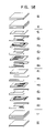
- FIG. 4A is a mimetic diagram showing that a magnetic layer or a non-magnetic layer is cast on a carrier film
- FIG. 4B is a mimetic diagram showing that a via hole and cutting lines are formed on a magnetic layer or a non-magnetic layer;
- FIG. 4C is a mimetic diagram showing that an electrode pattern is formed on a non-magnetic layer
- FIG. 4D is a mimetic diagram showing a non-magnetic layer of which unnecessary parts have been removed
- FIG. 4E is a mimetic diagram showing a magnetic layer of which unnecessary parts have been removed.
- FIG. 5A is a flow chart showing a stack of a chip type power inductor according to the present invention.
- FIG. 5B is a flow chart showing another stack of a chip type power inductor according to the present invention.
- FIG. 6A is a mimetic diagram showing a chip type power inductor fabricated by the process of FIG. 5A ;
- FIG. 6B is a mimetic diagram showing a chip type power inductor fabricated by the process of FIG. 5B ;
- FIG. 6C is a perspective view showing an inside of a fabricated chip type power inductor
- FIG. 6D is a sectional view showing an inside of a fabricated chip type power inductor.
- FIG. 6E is a chip type power inductor where an external electrode is formed.
- FIG. 1 shows one embodiment of a chip type power inductor.
- electrode patterns 12 are formed in a magnetic substance which forms a magnetic core 10 integrally formed as a plurality of magnetic layers are stacked.
- a magnetic saturation in a low current can not be prevented.
- FIG. 2A is a basic structure of a power inductor according to the present invention, in which a non-magnetic layer 24 is formed in the magnetic substance which forms a magnetic core 20 .
- the non-magnetic layer increases a magnetic resistance of the magnetic substance which forms a magnetic core and thus prevents a magnetic saturation from occurring in a low current.
- the magnetic substance which forms a magnetic core is constituted with several unit layers, and electrode patterns 22 are formed on each layer.
- the non-magnetic layer 24 is preferably inserted into one position between several layers constituting the magnetic substance which forms a magnetic core, and a thickness thereof is determined by considering an electric characteristic of the power inductor. Electrode patterns need not be formed on the non-magnetic layer, and via holes are preferably formed in order to electrically connect electrode patterns formed on the layers positioned at upper and lower surfaces of the non-magnetic layer one another.
- FIG. 2B is a sectional mimetic diagram showing a variation example of the power inductor of the present invention, in which the magnetic substance which forms a magnetic core where a plurality of layers are stacked is divided into a magnetic substance region 30 and a non-magnetic substance region 36 .
- the magnetic substance region is divided into a magnetic substance formed at a center surrounded by the non-magnetic substance regions and a magnetic substance formed at a periphery of the non-magnetic substance regions.
- a non-magnetic layer 34 is inserted into an inside of the magnetic substance which forms a magnetic core, and thereby shields a magnetic path of the magnetic substance which forms a magnetic core thus to increase a magnetic resistance likewise the embodiment shown in FIG. 2A .
- each region seems to be independent to each other, each region constitutes one layer at the time of a substantial fabrication and the layers are stacked to be integrally formed. Details of the fabrication process will be explained.
- electrode patterns 32 are formed on at least one surface between upper and lower surfaces of each layer constituting the non-magnetic substance region inside of the magnetic substance which forms a magnetic core. If the electrode patterns are formed on the non-magnetic layers having higher electric resistance and lower permeability and dielectric constant than magnetic material, an insulation degradation resulting from that a thickness of each layer becomes small can be prevented and a parasitic capacitance generation is restrained, thereby improving frequency characteristics.
- a following table 1 shows electric characteristics of the power inductor having each structure shown in FIGS. 1 , 2 A, and 2 B, and FIG. 3 shows the result as a graph.
- the magnetic saturation current is a current value at the time when a DC bias is applied and thereby an inductance value is reduced by 10%.
- the inductance is high compared to other structures but the magnetic saturation is generated at 50 mA.
- the magnetic saturation current value becomes great.
- the magnetic saturation current value exceeds 1A which is a value greater than that of the case that the non-magnetic layer is not inserted by more than 20 times.
- electrode patterns are formed on a plurality of magnetic sheets, the magnetic sheets are stacked, and a non-magnetic layer where the electrode patterns are not formed is inserted to the inside of the stacked sheets.
- FIG. 2B detail processes will be explained on the basis of a structure of the power inductor shown in FIG. 2B , and the processes can be applied to a structure shown in FIG. 2A .
- FIG. 4A shows a step of preparing green sheets.
- a magnetic layer or a non-magnetic layer 42 are formed on a carrier film 40 .
- the magnetic layer green sheet or the non-magnetic layer green sheet are respectively formed by using a doctor blade tape casting method used in a thick layer stacking process.
- As the carrier film a PET film is used and another materials can be used. The carrier film is picked up when each layer is sequentially stacked after a fabrication of each layer is completed.
- the green sheet that the magnetic layer or the non-magnetic layer are formed on the carrier film can be used as the cover layer by itself or by stacking several layers.
- cutting lines are formed constantly.
- the cutting lines are composed of an inner cutting line for a window 44 b and both lateral cutting lines 44 a .
- the cutting lines can be formed by a laser processing or a mechanical processing, in which the carrier film must not be damaged.
- a cutting processing of FIG. 4B is applied to both the magnetic layer green sheet and the non-magnetic layer green sheet.
- the magnetic layer green sheet or the non-magnetic layer green sheet where the cutting lines are formed can be used as a buffer layer by itself or by stacking several layers.
- the non-magnetic layer green sheet where the inner cutting line for a window is not formed is used as a non-magnetic layer inserted to an inside of the magnetic substance which forms a magnetic core by itself or by stacking several layers.
- a via hole 46 is formed besides the cutting lines 44 a and 44 b .
- the via hole is formed by using a laser punching or a mechanical punching.
- an electrode pattern 48 is formed on the non-magnetic 42 green sheet where the cutting lines and the via hole are formed.
- the electrode pattern can be formed as different patterns (for example, a pattern that an electrode pattern of a first sheet and an electrode pattern of a second sheet are symmetrical to each other) by an order of the non-magnetic electrode layer, and can be changed into various shapes according to a usage purpose of coil components.
- one end of the electrode pattern extends up to an end of the green sheet thus to be electrically connected to an external electrode.
- a conductive paste is printed on an upper surface of the non-magnetic green sheet by using a screen printing method thus to form the electrode pattern, and a conductive material is filled in the via hole 46 .
- one end of the electrode pattern 48 is connected to the via hole 46 .
- This form is a means to electrically connect each electrode pattern on the non-magnetic electrode layer by each layer.
- FIGS. 4D and 4E show the magnetic and non-magnetic green sheets where unnecessary parts are picked up. In FIG. 4D , a center region and a periphery region of the non-magnetic green sheet are picked up, and in FIG.
- a magnetic layer 42 b of the magnetic green sheet remains only at a region opposite to that of the non-magnetic green sheet.
- the magnetic layer green sheet of which a center magnetic layer is picked up shown in FIG. 4E and the non-magnetic layer green sheet where the inner cutting line for a window is not formed are inserted to an inside of the magnetic substance which forms a magnetic core, thereby being used as a non-magnetic layer.
- FIG. 5A shows a stack processing, in which each layer is sequentially stacked as one.
- a plurality of electrode layers that the magnetic layer 42 b and the non-magnetic layer 42 a constitute one layer between the cover layers 51 positioned at both ends are stacked.
- the cover layer is composed of a magnetic layer, but can be composed of a magnetic layer and a non-magnetic layer as another embodiment (Refer to FIG. 5B , 51 denotes a magnetic cover layer and 52 denotes a non-magnetic cover layer).
- the additional non-magnetic cover layer attenuates a minute thermal expansion rate difference between the magnetic layer and the non-magnetic layer generated at the time of a firing process thus to stabilizes a mechanical structure of a product.
- a non-magnetic layer 42 ′ where the electrode pattern is not formed can be used as a buffer layer in order to prevent electrode patterns formed on the non-magnetic layer from being in directly contact with the upper cover layer.
- the green sheet fabricated in FIGS. 4A and 4B and the green sheet where the cutting lines are formed are used as the cover layer and the buffer layer in a state that the carrier film is respectively picked-up.
- the non-magnetic layer 42 a and the magnetic layer 42 b fabricated in FIGS. 4D and 4E are alternately stacked thus to form an electrode layer. Even though the electrode layer is composed of four layers in drawings, more layers are preferably stacked.
- the non-magnetic layer 42 a and the magnetic layer 42 b are alternately stacked and thus exist in the same layer. By this stack, the electrode patterns formed on the non-magnetic layer are electrically connected to each other.
- one end of the electrode pattern ( 48 of FIG. 4C ) is connected to a via hole ( 46 of FIG. 4C ) thus to be electrically connected to another end of the electrode pattern of another layer.
- a non-magnetic layer 42 c where the electrode pattern is not formed is inserted between the stacked electrode layers thus to form a micro gap which shields a magnetic path inside of the stacked body.
- the non-magnetic layer 42 c constitutes one layer with a magnetic layer 42 b ′.
- the inner magnetic flux shielding layer is composed of one non-magnetic layer in drawings, several non-magnetic layers can be inserted according to electric characteristics of a final product.
- FIG. 6A shows a state that the stacking has been finished, in which an outwardly extended end 46 ′ of the electrode pattern can be seen.
- FIG. 6B shows that the non-magnetic cover layer 52 is additionally formed by the process of FIG. 5B .
- FIGS. 6C and 6D are perspective and sectional views showing inside of the fabricated power inductor.
- an electrode pattern of a coil form, an insulating region of a non-magnetic substance, and a magnetic path of a magnetic substance are formed.
- FIG. 6E shows a final product where the external electrodes have been formed.
- the chip type power inductor of the present invention can be economically fabricated and a large amount of devices can be fabricated fast.
- a magnetic flux inside of the power inductor can be controlled, so that a DC bias characteristic corresponding to several hundreds of mA ⁇ 1A which could not be realized by the conventional multi-layer chip power inductor can be obtained.
- a multi-layer power inductor of a very small size can be fabricated thus to be used in a notebook PC, another small communication devices, and electric instruments.
- a productivity is excellent thus to economically fabricate a large amount of products.
Landscapes
- Engineering & Computer Science (AREA)
- Power Engineering (AREA)
- Microelectronics & Electronic Packaging (AREA)
- Manufacturing & Machinery (AREA)
- Coils Or Transformers For Communication (AREA)
- Coils Of Transformers For General Uses (AREA)
- Manufacturing Cores, Coils, And Magnets (AREA)
Applications Claiming Priority (2)
| Application Number | Priority Date | Filing Date | Title |
|---|---|---|---|
| KR75680/2002 | 2002-11-30 | ||
| KR10-2002-0075680A KR100479625B1 (ko) | 2002-11-30 | 2002-11-30 | 칩타입 파워인덕터 및 그 제조방법 |
Publications (2)
| Publication Number | Publication Date |
|---|---|
| US20040108934A1 US20040108934A1 (en) | 2004-06-10 |
| US7069639B2 true US7069639B2 (en) | 2006-07-04 |
Family
ID=32464470
Family Applications (1)
| Application Number | Title | Priority Date | Filing Date |
|---|---|---|---|
| US10/723,753 Expired - Fee Related US7069639B2 (en) | 2002-11-30 | 2003-11-25 | Method of making chip type power inductor |
Country Status (5)
| Country | Link |
|---|---|
| US (1) | US7069639B2 (zh) |
| JP (1) | JP2004311944A (zh) |
| KR (1) | KR100479625B1 (zh) |
| CN (1) | CN1236459C (zh) |
| TW (1) | TWI242782B (zh) |
Cited By (18)
| Publication number | Priority date | Publication date | Assignee | Title |
|---|---|---|---|---|
| US20060236523A1 (en) * | 2003-10-02 | 2006-10-26 | Sulzer Euroflamm Us Inc | Friction facing method for use in a friction environment |
| US20070152793A1 (en) * | 2005-12-29 | 2007-07-05 | Lg Electronics Inc. | Chip-type inductor |
| US20070270069A1 (en) * | 2006-05-18 | 2007-11-22 | Sulzer Euroflamm Us Inc. | Friction material and system and method for making the friction material |
| US20080038562A1 (en) * | 2006-08-08 | 2008-02-14 | Murata Manufacturing Co., Ltd. | Layered coil component and method for manufacturing the layered coil component |
| US20080061917A1 (en) * | 2006-09-12 | 2008-03-13 | Cooper Technologies Company | Low profile layered coil and cores for magnetic components |
| US20090235459A1 (en) * | 2003-07-01 | 2009-09-24 | The Boppy Company, Llc | Booster accessory for support pillows |
| US20100007457A1 (en) * | 2008-07-11 | 2010-01-14 | Yipeng Yan | Magnetic components and methods of manufacturing the same |
| US20100026443A1 (en) * | 2008-07-29 | 2010-02-04 | Yipeng Yan | Magnetic Electrical Device |
| US20100108233A1 (en) * | 2008-10-31 | 2010-05-06 | Tdk Corporation | Method for producing multilayer inductor |
| US20100259351A1 (en) * | 2006-09-12 | 2010-10-14 | Robert James Bogert | Low profile layered coil and cores for magnetic components |
| US20100271161A1 (en) * | 2008-07-11 | 2010-10-28 | Yipeng Yan | Magnetic components and methods of manufacturing the same |
| US20100277267A1 (en) * | 2009-05-04 | 2010-11-04 | Robert James Bogert | Magnetic components and methods of manufacturing the same |
| US8310332B2 (en) | 2008-10-08 | 2012-11-13 | Cooper Technologies Company | High current amorphous powder core inductor |
| US8410884B2 (en) | 2011-01-20 | 2013-04-02 | Hitran Corporation | Compact high short circuit current reactor |
| US8659379B2 (en) | 2008-07-11 | 2014-02-25 | Cooper Technologies Company | Magnetic components and methods of manufacturing the same |
| US8941457B2 (en) | 2006-09-12 | 2015-01-27 | Cooper Technologies Company | Miniature power inductor and methods of manufacture |
| US9558881B2 (en) | 2008-07-11 | 2017-01-31 | Cooper Technologies Company | High current power inductor |
| US9589716B2 (en) | 2006-09-12 | 2017-03-07 | Cooper Technologies Company | Laminated magnetic component and manufacture with soft magnetic powder polymer composite sheets |
Families Citing this family (30)
| Publication number | Priority date | Publication date | Assignee | Title |
|---|---|---|---|---|
| KR100665114B1 (ko) * | 2005-01-07 | 2007-01-09 | 삼성전기주식회사 | 평면형 자성 인덕터의 제조 방법 |
| KR100596502B1 (ko) * | 2005-01-24 | 2006-07-05 | 한명희 | 적층형 칩 타이프 파워 인덕터 및 그 제조 방법 |
| KR100663242B1 (ko) * | 2005-06-29 | 2007-01-02 | 송만호 | 적층형 칩 타입 파워 인덕터 및 그 제조 방법 |
| JP2007157983A (ja) * | 2005-12-05 | 2007-06-21 | Taiyo Yuden Co Ltd | 積層インダクタ |
| KR20070070900A (ko) * | 2005-12-29 | 2007-07-04 | 엘지전자 주식회사 | 칩타입 인덕터 |
| EP1983531B1 (en) | 2006-01-31 | 2017-10-25 | Hitachi Metals, Ltd. | Laminate device and module comprising same |
| KR100776406B1 (ko) * | 2006-02-16 | 2007-11-16 | 삼성전자주식회사 | 마이크로 인덕터 및 그 제작 방법 |
| US8004381B2 (en) * | 2006-07-05 | 2011-08-23 | Hitachi Metals, Ltd. | Laminated device |
| KR101174541B1 (ko) * | 2007-02-02 | 2012-08-16 | 가부시키가이샤 무라타 세이사쿠쇼 | 적층 코일 부품 |
| JP4605192B2 (ja) * | 2007-07-20 | 2011-01-05 | セイコーエプソン株式会社 | コイルユニット及び電子機器 |
| KR100888437B1 (ko) | 2007-09-28 | 2009-03-11 | 삼성전기주식회사 | 칩 인덕터 제조방법 |
| KR101105651B1 (ko) * | 2007-12-07 | 2012-01-18 | 가부시키가이샤 무라타 세이사쿠쇼 | 적층형 전자 부품 |
| WO2009087928A1 (ja) * | 2008-01-08 | 2009-07-16 | Murata Manufacturing Co., Ltd. | 開磁路型積層コイル部品およびその製造方法 |
| CN101981635B (zh) | 2008-04-08 | 2013-09-25 | 株式会社村田制作所 | 电子元器件 |
| JP4873049B2 (ja) * | 2009-06-25 | 2012-02-08 | 株式会社村田製作所 | 電子部品 |
| CN102082019B (zh) * | 2010-12-01 | 2012-04-25 | 深圳市麦捷微电子科技股份有限公司 | 一种功率电感及其制造方法 |
| KR101214731B1 (ko) * | 2011-07-29 | 2012-12-21 | 삼성전기주식회사 | 적층형 인덕터 및 이의 제조 방법 |
| KR20130096026A (ko) * | 2012-02-21 | 2013-08-29 | 삼성전기주식회사 | 적층형 인덕터 및 그 제조 방법 |
| KR20130117026A (ko) * | 2012-04-17 | 2013-10-25 | 주식회사 이노칩테크놀로지 | 회로 보호 소자 |
| KR101952848B1 (ko) * | 2013-01-30 | 2019-02-27 | 삼성전기주식회사 | 인덕터 및 그 제조 방법 |
| KR101994724B1 (ko) * | 2013-11-05 | 2019-07-01 | 삼성전기주식회사 | 적층형 인덕터 및 그 제조방법 |
| KR101686989B1 (ko) | 2014-08-07 | 2016-12-19 | 주식회사 모다이노칩 | 파워 인덕터 |
| KR101681200B1 (ko) | 2014-08-07 | 2016-12-01 | 주식회사 모다이노칩 | 파워 인덕터 |
| WO2016021807A1 (ko) * | 2014-08-07 | 2016-02-11 | 주식회사 이노칩테크놀로지 | 파워 인덕터 |
| JP6569457B2 (ja) * | 2015-10-16 | 2019-09-04 | Tdk株式会社 | コイル部品及びその製造方法、並びに、コイル部品が実装された回路基板 |
| US10763031B2 (en) | 2016-08-30 | 2020-09-01 | Samsung Electro-Mechanics Co., Ltd. | Method of manufacturing an inductor |
| JP2021129074A (ja) * | 2020-02-17 | 2021-09-02 | 日東電工株式会社 | 枠部材付きインダクタおよび枠部材付き積層シート |
| KR102258927B1 (ko) | 2020-04-01 | 2021-05-31 | 한국세라믹기술원 | 자성체의 제조방법 |
| KR102404315B1 (ko) | 2020-05-08 | 2022-06-07 | 삼성전기주식회사 | 코일 부품 |
| CN112103059B (zh) * | 2020-09-15 | 2022-02-22 | 横店集团东磁股份有限公司 | 一种薄膜功率电感器的制作方法以及薄膜功率电感器 |
Citations (7)
| Publication number | Priority date | Publication date | Assignee | Title |
|---|---|---|---|---|
| US3765082A (en) * | 1972-09-20 | 1973-10-16 | San Fernando Electric Mfg | Method of making an inductor chip |
| US5479695A (en) * | 1991-05-02 | 1996-01-02 | At&T Corp. | Method of making a multilayer monolithic magnetic component |
| US6249205B1 (en) * | 1998-11-20 | 2001-06-19 | Steward, Inc. | Surface mount inductor with flux gap and related fabrication methods |
| US6293001B1 (en) * | 1994-09-12 | 2001-09-25 | Matsushita Electric Industrial Co., Ltd. | Method for producing an inductor |
| US6675462B1 (en) * | 1998-05-01 | 2004-01-13 | Taiyo Yuden Co., Ltd. | Method of manufacturing a multi-laminated inductor |
| US6917274B2 (en) * | 2002-10-01 | 2005-07-12 | Ceratech Corporation | Stacked coil device and fabrication method thereof |
| US6918173B2 (en) * | 2000-07-31 | 2005-07-19 | Ceratech Corporation | Method for fabricating surface mountable chip inductor |
Family Cites Families (4)
| Publication number | Priority date | Publication date | Assignee | Title |
|---|---|---|---|---|
| JPH09306770A (ja) * | 1996-05-20 | 1997-11-28 | Fuji Elelctrochem Co Ltd | 積層型チップトランスの製造方法 |
| JP2001230119A (ja) * | 2000-02-14 | 2001-08-24 | Murata Mfg Co Ltd | 積層インダクタ |
| JP3449351B2 (ja) * | 2000-11-09 | 2003-09-22 | 株式会社村田製作所 | 積層セラミック電子部品の製造方法及び積層セラミック電子部品 |
| JP3555598B2 (ja) * | 2001-06-27 | 2004-08-18 | 株式会社村田製作所 | 積層型インダクタ |
-
2002
- 2002-11-30 KR KR10-2002-0075680A patent/KR100479625B1/ko not_active IP Right Cessation
-
2003
- 2003-11-25 US US10/723,753 patent/US7069639B2/en not_active Expired - Fee Related
- 2003-11-28 TW TW092133495A patent/TWI242782B/zh not_active IP Right Cessation
- 2003-11-28 CN CNB2003101209410A patent/CN1236459C/zh not_active Expired - Fee Related
- 2003-12-01 JP JP2003401474A patent/JP2004311944A/ja active Pending
Patent Citations (7)
| Publication number | Priority date | Publication date | Assignee | Title |
|---|---|---|---|---|
| US3765082A (en) * | 1972-09-20 | 1973-10-16 | San Fernando Electric Mfg | Method of making an inductor chip |
| US5479695A (en) * | 1991-05-02 | 1996-01-02 | At&T Corp. | Method of making a multilayer monolithic magnetic component |
| US6293001B1 (en) * | 1994-09-12 | 2001-09-25 | Matsushita Electric Industrial Co., Ltd. | Method for producing an inductor |
| US6675462B1 (en) * | 1998-05-01 | 2004-01-13 | Taiyo Yuden Co., Ltd. | Method of manufacturing a multi-laminated inductor |
| US6249205B1 (en) * | 1998-11-20 | 2001-06-19 | Steward, Inc. | Surface mount inductor with flux gap and related fabrication methods |
| US6918173B2 (en) * | 2000-07-31 | 2005-07-19 | Ceratech Corporation | Method for fabricating surface mountable chip inductor |
| US6917274B2 (en) * | 2002-10-01 | 2005-07-12 | Ceratech Corporation | Stacked coil device and fabrication method thereof |
Cited By (28)
| Publication number | Priority date | Publication date | Assignee | Title |
|---|---|---|---|---|
| US20090235459A1 (en) * | 2003-07-01 | 2009-09-24 | The Boppy Company, Llc | Booster accessory for support pillows |
| US20060236523A1 (en) * | 2003-10-02 | 2006-10-26 | Sulzer Euroflamm Us Inc | Friction facing method for use in a friction environment |
| US20070152793A1 (en) * | 2005-12-29 | 2007-07-05 | Lg Electronics Inc. | Chip-type inductor |
| US7804389B2 (en) * | 2005-12-29 | 2010-09-28 | Lg Electronics Inc. | Chip-type inductor |
| US20070270069A1 (en) * | 2006-05-18 | 2007-11-22 | Sulzer Euroflamm Us Inc. | Friction material and system and method for making the friction material |
| US20080038562A1 (en) * | 2006-08-08 | 2008-02-14 | Murata Manufacturing Co., Ltd. | Layered coil component and method for manufacturing the layered coil component |
| US7474191B2 (en) * | 2006-08-08 | 2009-01-06 | Murata Manufacturing Co., Ltd. | Layered coil component and method for manufacturing the layered coil component |
| US20080061917A1 (en) * | 2006-09-12 | 2008-03-13 | Cooper Technologies Company | Low profile layered coil and cores for magnetic components |
| US9589716B2 (en) | 2006-09-12 | 2017-03-07 | Cooper Technologies Company | Laminated magnetic component and manufacture with soft magnetic powder polymer composite sheets |
| US8941457B2 (en) | 2006-09-12 | 2015-01-27 | Cooper Technologies Company | Miniature power inductor and methods of manufacture |
| US7791445B2 (en) | 2006-09-12 | 2010-09-07 | Cooper Technologies Company | Low profile layered coil and cores for magnetic components |
| US8466764B2 (en) | 2006-09-12 | 2013-06-18 | Cooper Technologies Company | Low profile layered coil and cores for magnetic components |
| US20100259351A1 (en) * | 2006-09-12 | 2010-10-14 | Robert James Bogert | Low profile layered coil and cores for magnetic components |
| US8484829B2 (en) | 2006-09-12 | 2013-07-16 | Cooper Technologies Company | Methods for manufacturing magnetic components having low probile layered coil and cores |
| US20100007457A1 (en) * | 2008-07-11 | 2010-01-14 | Yipeng Yan | Magnetic components and methods of manufacturing the same |
| US20100271161A1 (en) * | 2008-07-11 | 2010-10-28 | Yipeng Yan | Magnetic components and methods of manufacturing the same |
| US8279037B2 (en) | 2008-07-11 | 2012-10-02 | Cooper Technologies Company | Magnetic components and methods of manufacturing the same |
| US9859043B2 (en) * | 2008-07-11 | 2018-01-02 | Cooper Technologies Company | Magnetic components and methods of manufacturing the same |
| US9558881B2 (en) | 2008-07-11 | 2017-01-31 | Cooper Technologies Company | High current power inductor |
| US8659379B2 (en) | 2008-07-11 | 2014-02-25 | Cooper Technologies Company | Magnetic components and methods of manufacturing the same |
| US8378777B2 (en) | 2008-07-29 | 2013-02-19 | Cooper Technologies Company | Magnetic electrical device |
| US8910373B2 (en) | 2008-07-29 | 2014-12-16 | Cooper Technologies Company | Method of manufacturing an electromagnetic component |
| US20100026443A1 (en) * | 2008-07-29 | 2010-02-04 | Yipeng Yan | Magnetic Electrical Device |
| US8310332B2 (en) | 2008-10-08 | 2012-11-13 | Cooper Technologies Company | High current amorphous powder core inductor |
| US20100108233A1 (en) * | 2008-10-31 | 2010-05-06 | Tdk Corporation | Method for producing multilayer inductor |
| US8209849B2 (en) * | 2008-10-31 | 2012-07-03 | Tdk Corporation | Method for producing multilayer inductor |
| US20100277267A1 (en) * | 2009-05-04 | 2010-11-04 | Robert James Bogert | Magnetic components and methods of manufacturing the same |
| US8410884B2 (en) | 2011-01-20 | 2013-04-02 | Hitran Corporation | Compact high short circuit current reactor |
Also Published As
| Publication number | Publication date |
|---|---|
| CN1236459C (zh) | 2006-01-11 |
| KR20040047452A (ko) | 2004-06-05 |
| CN1505068A (zh) | 2004-06-16 |
| TWI242782B (en) | 2005-11-01 |
| JP2004311944A (ja) | 2004-11-04 |
| US20040108934A1 (en) | 2004-06-10 |
| TW200411687A (en) | 2004-07-01 |
| KR100479625B1 (ko) | 2005-03-31 |
Similar Documents
| Publication | Publication Date | Title |
|---|---|---|
| US7069639B2 (en) | Method of making chip type power inductor | |
| US6917274B2 (en) | Stacked coil device and fabrication method thereof | |
| KR101670184B1 (ko) | 적층 전자부품 및 그 제조방법 | |
| KR101462806B1 (ko) | 인덕터 및 그 제조 방법 | |
| KR100534169B1 (ko) | 적층 인덕터 및 그 제조 방법 | |
| JP3621300B2 (ja) | 電源回路用積層インダクタ | |
| US9251943B2 (en) | Multilayer type inductor and method of manufacturing the same | |
| JP2014022724A (ja) | パワーインダクタ用磁性体モジュール、パワーインダクタ及びその製造方法 | |
| KR20170032057A (ko) | 적층 전자부품 | |
| KR20150042499A (ko) | 적층형 인덕터 및 그 제조 방법 | |
| TWI609385B (zh) | 一多層電感器及其製造方法 | |
| KR20190021686A (ko) | 코일 부품 및 그 제조방법 | |
| KR20170032056A (ko) | 적층 전자부품 및 그 제조방법 | |
| JP2002190410A (ja) | 積層型トランス | |
| JP2005045103A (ja) | チップインダクタ | |
| KR101026034B1 (ko) | 칩 형상의 파워 인덕터 | |
| CN109643606A (zh) | 电感元件和制造电感元件的方法 | |
| KR100614259B1 (ko) | 적층형 파워인덕터 | |
| KR100344626B1 (ko) | 칩 인덕터 | |
| KR102004815B1 (ko) | 파워 인덕터용 자성체 모듈, 파워 인덕터 및 그 제조 방법 | |
| CN219626456U (zh) | 一种具有磁屏蔽结构的叠层片式共模电感器 | |
| US20220262558A1 (en) | Laminated coil component | |
| KR100431175B1 (ko) | 복수의 권선이 형성된 칩인덕터 | |
| JP2001285005A (ja) | ノイズフィルタ | |
| KR100384457B1 (ko) | 칩 인덕터 |
Legal Events
| Date | Code | Title | Description |
|---|---|---|---|
| AS | Assignment |
Owner name: CERATECH CORPORATION, KOREA, REPUBLIC OF Free format text: ASSIGNMENT OF ASSIGNORS INTEREST;ASSIGNORS:CHOI, MYOUNG-HUI;HONG, SOON-GYU;JANG, SANG-EUN;REEL/FRAME:014751/0986;SIGNING DATES FROM 20030926 TO 20031001 |
|
| FPAY | Fee payment |
Year of fee payment: 4 |
|
| REMI | Maintenance fee reminder mailed | ||
| LAPS | Lapse for failure to pay maintenance fees | ||
| STCH | Information on status: patent discontinuation |
Free format text: PATENT EXPIRED DUE TO NONPAYMENT OF MAINTENANCE FEES UNDER 37 CFR 1.362 |
|
| FP | Lapsed due to failure to pay maintenance fee |
Effective date: 20140704 |